WO2016181812A1 - ガラス及びガラス部材 - Google Patents
ガラス及びガラス部材 Download PDFInfo
- Publication number
- WO2016181812A1 WO2016181812A1 PCT/JP2016/062910 JP2016062910W WO2016181812A1 WO 2016181812 A1 WO2016181812 A1 WO 2016181812A1 JP 2016062910 W JP2016062910 W JP 2016062910W WO 2016181812 A1 WO2016181812 A1 WO 2016181812A1
- Authority
- WO
- WIPO (PCT)
- Prior art keywords
- glass
- light
- less
- light emitting
- guide plate
- Prior art date
- Legal status (The legal status is an assumption and is not a legal conclusion. Google has not performed a legal analysis and makes no representation as to the accuracy of the status listed.)
- Ceased
Links
Images



Classifications
-
- C—CHEMISTRY; METALLURGY
- C03—GLASS; MINERAL OR SLAG WOOL
- C03C—CHEMICAL COMPOSITION OF GLASSES, GLAZES OR VITREOUS ENAMELS; SURFACE TREATMENT OF GLASS; SURFACE TREATMENT OF FIBRES OR FILAMENTS MADE FROM GLASS, MINERALS OR SLAGS; JOINING GLASS TO GLASS OR OTHER MATERIALS
- C03C4/00—Compositions for glass with special properties
- C03C4/0092—Compositions for glass with special properties for glass with improved high visible transmittance, e.g. extra-clear glass
-
- B—PERFORMING OPERATIONS; TRANSPORTING
- B32—LAYERED PRODUCTS
- B32B—LAYERED PRODUCTS, i.e. PRODUCTS BUILT-UP OF STRATA OF FLAT OR NON-FLAT, e.g. CELLULAR OR HONEYCOMB, FORM
- B32B17/00—Layered products essentially comprising sheet glass, or glass, slag, or like fibres
- B32B17/06—Layered products essentially comprising sheet glass, or glass, slag, or like fibres comprising glass as the main or only constituent of a layer, next to another layer of a specific material
- B32B17/10—Layered products essentially comprising sheet glass, or glass, slag, or like fibres comprising glass as the main or only constituent of a layer, next to another layer of a specific material of synthetic resin
-
- C—CHEMISTRY; METALLURGY
- C03—GLASS; MINERAL OR SLAG WOOL
- C03C—CHEMICAL COMPOSITION OF GLASSES, GLAZES OR VITREOUS ENAMELS; SURFACE TREATMENT OF GLASS; SURFACE TREATMENT OF FIBRES OR FILAMENTS MADE FROM GLASS, MINERALS OR SLAGS; JOINING GLASS TO GLASS OR OTHER MATERIALS
- C03C3/00—Glass compositions
- C03C3/04—Glass compositions containing silica
- C03C3/076—Glass compositions containing silica with 40% to 90% silica, by weight
- C03C3/083—Glass compositions containing silica with 40% to 90% silica, by weight containing aluminium oxide or an iron compound
- C03C3/085—Glass compositions containing silica with 40% to 90% silica, by weight containing aluminium oxide or an iron compound containing an oxide of a divalent metal
- C03C3/087—Glass compositions containing silica with 40% to 90% silica, by weight containing aluminium oxide or an iron compound containing an oxide of a divalent metal containing calcium oxide, e.g. common sheet or container glass
-
- C—CHEMISTRY; METALLURGY
- C03—GLASS; MINERAL OR SLAG WOOL
- C03C—CHEMICAL COMPOSITION OF GLASSES, GLAZES OR VITREOUS ENAMELS; SURFACE TREATMENT OF GLASS; SURFACE TREATMENT OF FIBRES OR FILAMENTS MADE FROM GLASS, MINERALS OR SLAGS; JOINING GLASS TO GLASS OR OTHER MATERIALS
- C03C3/00—Glass compositions
- C03C3/04—Glass compositions containing silica
- C03C3/076—Glass compositions containing silica with 40% to 90% silica, by weight
- C03C3/089—Glass compositions containing silica with 40% to 90% silica, by weight containing boron
- C03C3/091—Glass compositions containing silica with 40% to 90% silica, by weight containing boron containing aluminium
-
- G—PHYSICS
- G02—OPTICS
- G02B—OPTICAL ELEMENTS, SYSTEMS OR APPARATUS
- G02B6/00—Light guides; Structural details of arrangements comprising light guides and other optical elements, e.g. couplings
- G02B6/0001—Light guides; Structural details of arrangements comprising light guides and other optical elements, e.g. couplings specially adapted for lighting devices or systems
- G02B6/0011—Light guides; Structural details of arrangements comprising light guides and other optical elements, e.g. couplings specially adapted for lighting devices or systems the light guides being planar or of plate-like form
-
- G—PHYSICS
- G02—OPTICS
- G02B—OPTICAL ELEMENTS, SYSTEMS OR APPARATUS
- G02B6/00—Light guides; Structural details of arrangements comprising light guides and other optical elements, e.g. couplings
- G02B6/0001—Light guides; Structural details of arrangements comprising light guides and other optical elements, e.g. couplings specially adapted for lighting devices or systems
- G02B6/0011—Light guides; Structural details of arrangements comprising light guides and other optical elements, e.g. couplings specially adapted for lighting devices or systems the light guides being planar or of plate-like form
- G02B6/0033—Means for improving the coupling-out of light from the light guide
- G02B6/0035—Means for improving the coupling-out of light from the light guide provided on the surface of the light guide or in the bulk of it
- G02B6/004—Scattering dots or dot-like elements, e.g. microbeads, scattering particles, nanoparticles
- G02B6/0043—Scattering dots or dot-like elements, e.g. microbeads, scattering particles, nanoparticles provided on the surface of the light guide
-
- G—PHYSICS
- G02—OPTICS
- G02B—OPTICAL ELEMENTS, SYSTEMS OR APPARATUS
- G02B6/00—Light guides; Structural details of arrangements comprising light guides and other optical elements, e.g. couplings
- G02B6/0001—Light guides; Structural details of arrangements comprising light guides and other optical elements, e.g. couplings specially adapted for lighting devices or systems
- G02B6/0011—Light guides; Structural details of arrangements comprising light guides and other optical elements, e.g. couplings specially adapted for lighting devices or systems the light guides being planar or of plate-like form
- G02B6/0033—Means for improving the coupling-out of light from the light guide
- G02B6/005—Means for improving the coupling-out of light from the light guide provided by one optical element, or plurality thereof, placed on the light output side of the light guide
- G02B6/0051—Diffusing sheet or layer
-
- G—PHYSICS
- G02—OPTICS
- G02B—OPTICAL ELEMENTS, SYSTEMS OR APPARATUS
- G02B6/00—Light guides; Structural details of arrangements comprising light guides and other optical elements, e.g. couplings
- G02B6/0001—Light guides; Structural details of arrangements comprising light guides and other optical elements, e.g. couplings specially adapted for lighting devices or systems
- G02B6/0011—Light guides; Structural details of arrangements comprising light guides and other optical elements, e.g. couplings specially adapted for lighting devices or systems the light guides being planar or of plate-like form
- G02B6/0033—Means for improving the coupling-out of light from the light guide
- G02B6/005—Means for improving the coupling-out of light from the light guide provided by one optical element, or plurality thereof, placed on the light output side of the light guide
- G02B6/0055—Reflecting element, sheet or layer
-
- G—PHYSICS
- G02—OPTICS
- G02F—OPTICAL DEVICES OR ARRANGEMENTS FOR THE CONTROL OF LIGHT BY MODIFICATION OF THE OPTICAL PROPERTIES OF THE MEDIA OF THE ELEMENTS INVOLVED THEREIN; NON-LINEAR OPTICS; FREQUENCY-CHANGING OF LIGHT; OPTICAL LOGIC ELEMENTS; OPTICAL ANALOGUE/DIGITAL CONVERTERS
- G02F1/00—Devices or arrangements for the control of the intensity, colour, phase, polarisation or direction of light arriving from an independent light source, e.g. switching, gating or modulating; Non-linear optics
- G02F1/01—Devices or arrangements for the control of the intensity, colour, phase, polarisation or direction of light arriving from an independent light source, e.g. switching, gating or modulating; Non-linear optics for the control of the intensity, phase, polarisation or colour
- G02F1/13—Devices or arrangements for the control of the intensity, colour, phase, polarisation or direction of light arriving from an independent light source, e.g. switching, gating or modulating; Non-linear optics for the control of the intensity, phase, polarisation or colour based on liquid crystals, e.g. single liquid crystal display cells
- G02F1/133—Constructional arrangements; Operation of liquid crystal cells; Circuit arrangements
- G02F1/1333—Constructional arrangements; Manufacturing methods
- G02F1/1335—Structural association of cells with optical devices, e.g. polarisers or reflectors
- G02F1/1336—Illuminating devices
- G02F1/133602—Direct backlight
- G02F1/133606—Direct backlight including a specially adapted diffusing, scattering or light controlling members
Definitions
- the present invention relates to glass and glass members.
- liquid crystal display devices are provided in portable information terminals such as liquid crystal televisions, tablet terminals, and smartphones.
- the liquid crystal display device has a planar light emitting device as a backlight and a liquid crystal panel disposed on the light emitting surface side of the planar light emitting device.
- planar light emitting devices There are two types of planar light emitting devices: a direct type and an edge light type, but an edge light type that can reduce the size of the light source is often used.
- the edge light type planar light emitting device includes a light source, a light guide plate, a reflection sheet, a diffusion sheet, and the like.
- a light incident end surface also simply referred to as a light incident surface
- a plurality of reflective dots are formed on a light reflecting surface which is a surface opposite to the light emitting surface facing the liquid crystal panel.
- the reflection sheet is arranged to face the light reflection surface
- the diffusion sheet is arranged to face the light emission surface.
- the light incident on the light guide plate from the light source travels while being reflected by the reflective dots and the reflective sheet, and is emitted from the light exit surface.
- the light emitted from the light exit surface is diffused by the diffusion sheet and then enters the liquid crystal panel.
- glass having high transmittance and excellent heat resistance can be used (see Patent Documents 1 and 2).
- a diffusion sheet is arrange
- the diffusion sheet is not properly disposed on the light emitting surface, and the phenomenon that the luminance of the emitted light varies greatly depending on the location (hereinafter referred to as luminance unevenness) has been a problem.
- a functional sheet-like material made of a resin material or the like for example, a scattering prevention sheet or a surface protection sheet
- a functional sheet-like material made of a resin material or the like for example, a scattering prevention sheet or a surface protection sheet
- One of the exemplary purposes of an aspect of the present invention is to provide a glass and a glass member capable of appropriately arranging a sheet-like material such as a diffusion sheet on the main surface.
- An absorption coefficient of light having a wavelength of 550 nm is 1 m ⁇ 1 or less, and a maximum value ⁇ max (m ⁇ 1 ) and a minimum value ⁇ min (m ⁇ 1 ) of light absorption coefficient in a wavelength range of 400 to 780 nm are
- the ratio ( ⁇ max / ⁇ min ) is 10 or less
- the two-dimensional arithmetic average height in an arbitrary 1790 ⁇ m ⁇ 1330 ⁇ m region on the first surface is 1 nm or less.
- a sheet-like object such as a diffusion sheet can be appropriately arranged on the main surface.
- FIG. 1 shows a liquid crystal display device 1 using glass as a light guide plate according to an embodiment of the present invention.
- the liquid crystal display device 1 is mounted on an electronic device that is reduced in size and thickness, such as a portable information terminal.
- the liquid crystal display device 1 has a liquid crystal panel 2 and a planar light emitting device 3.
- the liquid crystal panel 2 includes an alignment layer, a transparent electrode, a glass substrate, and a polarizing filter so as to sandwich a liquid crystal layer disposed in the center.
- a color filter is disposed on one side of the liquid crystal layer.
- the molecules of the liquid crystal layer rotate around the light distribution axis by applying a driving voltage to the transparent electrode, thereby performing a predetermined display.
- the planar light emitting device 3 adopts an edge light type in order to reduce the size and thickness.
- the planar light emitting device 3 includes a light source 4, a light guide plate 5, a reflection sheet 6, a diffusion sheet 7, and reflection dots 10A to 10C.
- the light incident on the light guide plate 5 from the light source 4 travels while being reflected by the reflection dots 10A to 10C and the reflection sheet 6, and is emitted from the light emission surface 51 of the light guide plate 5 facing the liquid crystal panel 2.
- the light emitted from the light emitting surface 51 is diffused by the diffusion sheet 7 and then enters the liquid crystal panel 2.
- the light source 4 is not particularly limited, and a hot cathode tube, a cold cathode tube, or an LED (Light Emitting Diode) can be used.
- the light source 4 is disposed so as to face the light incident surface 53 of the light guide plate 5.
- a reflector 8 is provided on the back side of the light source 4 in order to increase the incident efficiency of the light emitted radially from the light source 4 to the light guide plate 5.
- the reflection sheet 6 is configured such that a light reflection member is coated on the surface of a resin sheet such as an acrylic resin.
- the reflection sheet 6 is disposed on the light reflection surface 52 and the non-light-incident surfaces 54, 55 and 56 (55 is a surface opposite to 54) of the light guide plate 5.
- the light reflecting surface 52 is a surface opposite to the light emitting surface 51 of the light guide plate 5.
- the non-light incident surfaces 54 to 56 are surfaces other than the light reflection surface 52 and the light incident surface 53 at the end surface of the light guide plate 5. If it is not necessary to particularly increase the incident efficiency, the reflection sheet 6 may be configured not to be disposed on the non-light-incident surfaces 54 to 56.
- the diffusion sheet 7 can be a milky white acrylic resin film or the like. Since the diffusion sheet 7 diffuses the light emitted from the light emitting surface 51 of the light guide plate 5, the back side of the liquid crystal panel 2 can be irradiated with uniform light without uneven brightness.
- the diffusion sheet 7 is disposed on the light exit surface 51 of the light guide plate 5. As described above, when the diffusion sheet 7 is disposed on the light emitting surface 51, luminance unevenness occurs unless the diffusion sheet 7 is properly disposed.
- a glass member is composed of glass constituting the light guide plate 5 and a functional resin sheet containing a resin material as a main component.
- the functional resin sheet can be selected from the reflection sheet 6 or the diffusion sheet 7.
- such a glass member is used as the planar light emitting device 3.
- the glass member may be provided with reflective dots 10A to 10C.
- the coefficient of static friction between the light emitting surface 51 of the light guide plate 5 and the diffusion sheet 7 is preferably 0.20 or less.
- the static friction coefficient is preferably 0.20 or less.
- the dynamic friction coefficient between the light emitting surface 51 of the light guide plate 5 and the functional resin sheet such as the diffusion sheet 7 is preferably 0.20 or less.
- the glass of the present embodiment has a first surface and a second surface facing the first surface.
- the first surface can be the light emitting surface 51 and the second surface can be the light reflecting surface 52.
- the two-dimensional arithmetic average height (Sa) of the first surface of the glass of this embodiment is 1 nm or less in an arbitrary 1790 ⁇ m ⁇ 1330 ⁇ m region (hereinafter referred to as a wide region) on the first surface.
- the two-dimensional arithmetic average height (Sa) conforms to ISO 25178.
- the two-dimensional arithmetic average height (Sa) of the first surface of the glass of the present embodiment is 0.4 nm or less in an arbitrary 94 ⁇ m ⁇ 70 ⁇ m region (hereinafter referred to as a narrow region) on the first surface.
- the two-dimensional arithmetic average height (Sa) conforms to ISO 25178.
- the two-dimensional arithmetic average height (Sa) in a wide region and a narrow region of the first surface of the glass of the present embodiment can be adjusted by a substance added to the glass raw material.
- Alkaline earth metal oxides such as MgO, CaO, SrO, and BaO promote melting of glass raw materials, adjust thermal expansion, viscosity, etc., and reduce the two-dimensional arithmetic average height of the formed glass. It is a useful component.
- the total content of alkaline earth metal oxides is glass.
- composition A it is preferably 10% by mass or more, more preferably 13% by mass or more
- glass composition B it is 1% by mass or more, more preferably 10% by mass or more
- C it is preferably 5% by mass or more, more preferably 10% by mass or more.
- the glass of the present embodiment has an absorption coefficient of light having a wavelength of 550 nm of 1 m ⁇ 1 or less. The reason why the absorption coefficient of light having a wavelength of 550 nm is used as a judgment index is that the absorption coefficient of light having a wavelength of 550 nm is generally the highest among the light in the wavelength range of 400 to 700 nm.
- the absorption of light of three colors R (red), G (green), and B (blue), which is used as a light source of a liquid crystal television in which the planar light emitting device is an edge light system, is minimal.
- the maximum value ⁇ max of the light absorption coefficient in the wavelength range of 400 to 780 nm is preferably 1 m ⁇ 1 or less.
- the ratio ( ⁇ max / ⁇ min ) of the maximum value ⁇ max (m ⁇ 1 ) and the minimum value ⁇ min (m ⁇ 1 ) of the light absorption coefficient in the wavelength range of 400 to 780 nm is 10 or less. .
- the reason why the light absorption coefficient in the wavelength range of 400 to 780 nm is used as a judgment index is that it includes the wavelengths of light of three colors of R (red), G (green), and B (blue).
- the absorption of light of three colors of R (red), G (green), and B (blue), which is used as a light source for a liquid crystal television in which the planar light emitting device is an edge light system becomes light and has a wavelength of 400-
- the difference in light absorption depending on the wavelength in the range of 780 nm is also slight.
- the main factor of light absorption of glass is iron ions contained as impurities. Iron is unavoidably contained as a raw material for industrially produced glass, and it is inevitable that iron is mixed into the glass.
- the content of total iron oxide (t-Fe 2 O 3 ) converted to Fe 2 O 3 in the glass of this embodiment is 80 ppm by mass or less in order to realize extremely high transmittance over the entire visible range.
- the content of t-Fe 2 O 3 is more preferably 60 ppm by mass or less, further preferably 50 ppm by mass or less, particularly preferably 40 ppm by mass or less, and most preferably 35 ppm by mass or less. .
- the amount of t-Fe 2 O 3 in the glass of this embodiment is 1 mass ppm or more. If it is less than 1 mass ppm, it becomes difficult to improve the meltability of the glass during the production of the multi-component oxide glass, and it is difficult to mass-produce at a low cost. Moreover, it is difficult to obtain raw materials. Preferably it is 5 mass ppm or more, More preferably, it is 8 mass ppm or more, More preferably, it is 10 mass ppm or more.
- the amount of t-Fe 2 O 3 in the glass can be adjusted by the amount of iron component added during glass production.
- the total iron oxide content of the glass is expressed as the amount of Fe 2 O 3 , but not all the iron present in the glass exists as Fe 3+ (trivalent iron). Absent. Usually, Fe 3+ and Fe 2+ (divalent iron) are simultaneously present in the glass (hereinafter, these are collectively referred to as “iron component”). Although iron component has an absorption in the visible light region, the absorption coefficient of the Fe 2+ (11cm -1 Mol -1), since an order of magnitude greater than the absorption coefficient of the Fe 3+ (0.96cm -1 Mol -1) , visible The internal transmittance of the light region is further reduced. Therefore, it is preferable that the Fe 2+ content is small in order to increase the internal transmittance in the visible light region.
- the content of divalent iron (Fe 2+ ) converted to Fe 2 O 3 in terms of mass ppm is suppressed to 10 mass ppm or less.
- it is 8.0 mass ppm or less, More preferably, it is 6.0 mass ppm or less, More preferably, it is 4.0 mass ppm or less, Most preferably, it is 3.5 mass ppm or less.
- the minimum value of the internal transmittance of the glass in the wavelength range of 400 to 700 nm is 80% or more under the condition of an optical path length of 200 mm. The difference between the maximum value and the minimum value of the internal transmittance is preferably 15% or less.
- optical path length refers to the distance from the end face where light enters to the end face on the opposite side.
- the internal transmittance of glass at an optical path length of 200 mm can be measured as follows.
- the glass is cut out so that the optical path length becomes 200 mm, and is polished so that the surface roughness Ra of the surface on which single wavelength light described later is incident and the surface that is opposite to the surface is 0.03 ⁇ m or less.
- each single wavelength light of 400 to 780 nm is incident in 1 nm increments perpendicularly to the polished surface and emitted. Measure the intensity of single wavelength light. And the transmittance
- the minimum value of the internal transmittance is preferably 85% or more, and the difference between the maximum value and the minimum value of the internal transmittance is more preferably 13% or less. More preferably, the minimum value is 90% or more, and the difference between the maximum value and the minimum value of the internal transmittance is 8% or less.
- Glass composition Although the composition of the glass in this embodiment is not specifically limited, The following three types (glass which has glass composition A, glass composition B, and glass composition C) are mentioned as a typical example.
- a glass plate having the glass composition A is substantially expressed in terms of a mass percentage based on oxide, and is substantially 60 to 80% SiO 2 , 0 to 7% Al 2 O 3 , 0 to 10% MgO, CaO 0-20%, SrO 0-15%, BaO 0-15%, Na 2 O 3-20%, and K 2 O 0-10%.
- the glass plate having the glass composition B is substantially expressed in terms of mass percentage on the basis of oxide, and the SiO 2 is substantially 45 to 80%, the Al 2 O 3 is more than 7% and not more than 30%, and the B 2 O 3 is 0 ⁇ 15%, MgO 0 ⁇ 15%, CaO 0 ⁇ 6%, SrO 0 ⁇ 5%, BaO 0 ⁇ 5%, Na 2 O 7 ⁇ 20%, K 2 O 0 ⁇ 10%, And 0-10% of ZrO 2 .
- a glass plate having a glass composition C is substantially 45 to 70% of SiO 2 , 10 to 30% of Al 2 O 3 , and 0 to 15 of B 2 O 3 in terms of an oxide-based mass percentage. And at least one component selected from the group consisting of MgO, CaO, SrO and BaO, and a total of 5 to 30%, and at least selected from the group consisting of Li 2 O, Na 2 O and K 2 O One kind of component may be included in a total of 0% or more and less than 3%.
- the glass used for the light guide plate 5 of the present embodiment uses glass having low light absorption and good internal transmittance.
- the surface resistance on the first surface of the glass of this embodiment is preferably 2.5 ⁇ 10 14 ⁇ / ⁇ or less.
- the surface resistance is 2.5 ⁇ 10 14 ⁇ / ⁇ or less, static electricity generated on the first surface easily flows to the outside of the first surface.
- functional resin sheets, such as the diffusion sheet 7 are arrange
- the total content of alkali metal oxides is preferably 5 in the glass compositions A and B.
- the glass composition C it is preferably 0 to 2% by mass, and more preferably 0 to 1% by mass.
- the glass described above is suitable for use as the light guide plate 5 because of its good light absorption and internal transmittance. However, even if it is used as glass having good characteristics, if the diffusion sheet 7 is not properly disposed on the light exit surface 51 of the light guide plate 5, unevenness in brightness of the emitted light occurs depending on the location. .
- the present inventor conducted the following experiment paying attention to the surface roughness and electrical characteristics of the light emitting surface 51 of the light emitting surface 51.
- the evaluation of the surface roughness is made with an arbitrary 94 ⁇ m ⁇ 70 ⁇ m region (narrow region) on the light emitting surface 51 and an arbitrary 1790 ⁇ m ⁇ 1330 ⁇ m region (wide region) on the light emitting surface 51 wider than this. I went to two areas. In a wide area, the undulation generated on the light exit surface 51 can be measured. Further, in a narrow region, it is possible to measure fine irregularities generated on this undulation.
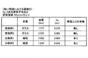
- FIG. 2 shows the experimental results of evaluating the surface roughness of a narrow region of the light emitting surface 51
- FIG. 3 shows the experimental results of evaluating the surface roughness of a wide region of the light emitting surface 51.
- Example 1 is expressed by mass%, SiO 2 69.8%, Al 2 O 3 3.2%, Na 2 O 11.1%, MgO 0.1%, CaO 7.9%, SrO. 3.9%, BaO 4.0%, and t-Fe 2 O 3 0.003%.
- Example 2 SiO 2 is 68.1% by mass%, Al 2 O 3 is 11.1%, B 2 O 3 is 9.1%, MgO is 2.4%, CaO is 8.7%, It is a glass containing 0.6% SrO and 0.005% t-Fe 2 O 3 .
- Comparative Example 1 is an SA light guide (manufactured by Sumika Acrylic Sales Co., Ltd.), and Comparative Example 2 is Denka TX polymer (manufactured by Denki Kagaku Kogyo Co., Ltd.).
- each sample evaluated for surface roughness is used as a light guide plate 5, and a reflection sheet 6 is provided on the sample to prepare a liquid crystal display device 1, and it is examined whether or not luminance unevenness occurs in each liquid crystal display device 1. An experiment was also conducted.
- the two-dimensional surface roughness (Sa) is as low as 0.4 nm or less compared to Comparative Examples 1 and 2. Further, in all the liquid crystal display devices 1 using Examples 1 and 2, luminance unevenness did not occur.
- the two-dimensional surface roughness (Sa) is as low as 1.0 nm or less compared to Comparative Examples 1 and 2. Further, in all the liquid crystal display devices 1 using Examples 1 and 2, luminance unevenness did not occur.
- the surface resistance of the light exit surface 51 was measured.
- the surface resistance was measured according to JIS K 6911.
- the static friction coefficient and the dynamic friction coefficient between the light emitting surface 51 and the diffusion sheet 7 of each sample for which the surface resistance was measured were obtained.
- the static friction coefficient and the dynamic friction coefficient were obtained by performing a test with a load of 300 gf ( ⁇ 2.94 N) and a speed of 1 mm / sec using a continuous load type scratch strength tester TYPE 18 (manufactured by Shinto Kagaku Co., Ltd.). .
- each sample for which the surface resistance is measured is used as the light guide plate 5, and the liquid crystal display device 1 is prepared by disposing a diffusion sheet 7 on the light guide plate 5, and whether or not luminance unevenness occurs in each liquid crystal display device 1. An experiment was also conducted.
- FIG. 4 shows the measurement results of the surface resistance of the light exit surface 51, the values of the static friction coefficient and the dynamic friction coefficient between the light exit surface 51 and the diffusion sheet 7, and the presence or absence of occurrence of uneven brightness.
- the coefficient of static friction between the light emitting surface 51 and the diffusion sheet 7 also becomes as large as 0.24 or more, and it becomes difficult to properly arrange the diffusion sheet 7 on the upper surface of the light emitting surface 51. It is considered that the luminance unevenness is caused by adsorption between the light emitting surface 51 and the diffusion sheet 7 due to static electricity generated due to an increase in surface resistance.
- Examples 1 and 2 made of glass the surface resistance is 2.5 ⁇ 10 14 ⁇ / ⁇ or less as compared with Comparative Examples 1 and 2. Therefore, the static electricity generated on the surface of the light emitting surface 51 flows outside the light emitting surface 51 because of its low electrical resistance, and therefore it is possible to prevent the diffusion sheet 7 from being attracted to the light emitting surface 51 due to static electricity. . Therefore, in Examples 1 and 2, the static friction coefficient between the light emitting surface 51 and the diffusion sheet 7 is as small as 0.20 or less. For this reason, in the liquid crystal display device 1 using Examples 1 and 2, luminance unevenness did not occur.
- the surface resistance of the main surface of glass used as the light guide plate 5 (surface that becomes the light emitting surface 51) is 2.5 ⁇ 10 14 ⁇ / ⁇ It was found that the following is desirable. Moreover, in order to suppress generation
- the present invention can be widely used for glass in which a functional sheet-like material made of a resin material or the like (for example, a diffusion sheet, a scattering prevention sheet, or a surface protection sheet) needs to be appropriately disposed on the main surface.
- a functional sheet-like material made of a resin material or the like for example, a diffusion sheet, a scattering prevention sheet, or a surface protection sheet
Landscapes
- Physics & Mathematics (AREA)
- Chemical & Material Sciences (AREA)
- General Physics & Mathematics (AREA)
- Optics & Photonics (AREA)
- Geochemistry & Mineralogy (AREA)
- Engineering & Computer Science (AREA)
- Chemical Kinetics & Catalysis (AREA)
- General Chemical & Material Sciences (AREA)
- Life Sciences & Earth Sciences (AREA)
- Materials Engineering (AREA)
- Organic Chemistry (AREA)
- Nonlinear Science (AREA)
- Mathematical Physics (AREA)
- Crystallography & Structural Chemistry (AREA)
- Planar Illumination Modules (AREA)
- Glass Compositions (AREA)
Abstract
Description
第1面と、
前記第1面に対向する第2面とを有するガラスであって、
波長550nmの光の吸収係数が1m-1以下であり、波長400~780nmの範囲の光の吸収係数の最大値αmax(m-1)と、最小値αmin(m-1)と、の比(αmax/αmin)が10以下であり、
前記第1面上の任意の1790μm×1330μm領域における2次元算術平均高さが1nm以下とする。
[面状発光装置の構造説明]
図1は、本発明のある実施形態であるガラスを導光板として用いた液晶表示装置1を示している。液晶表示装置1は、例えば携帯情報端末等の小型・薄型化が図られた電子機器に搭載される。
[表面粗さ]
本実施形態のガラスは、第1面と、第1面に対向する第2面を有する。本実施形態のガラスを導光板5として用いる場合、例えば第1面を光出射面51、第2面を光反射面52とすることができる。
[光の吸収係数]
本実施形態のガラスは、波長550nmの光の吸収係数が1m-1以下である。波長550nmの光の吸収係数を判断指標とするのは、波長400~700nmの範囲の光のうち、波長550nmの光の吸収係数が一般的に最も高くなるからである。
[光吸収]
ガラスの光吸収の主要因は、不純物として含まれる鉄イオンである。鉄は、工業的に生産されるガラスの原料として不可避的に含有されるものであり、ガラス中への鉄の混入は避けられない。
[内部透過率]
本実施形態のガラスにおいてさらに光吸収度を低減し高い透明度を得るためには、光路長200mmの条件下で、波長400~700nmの範囲におけるガラスの内部透過率の最小値が80%以上であり、内部透過率の最大値と最小値の差が15%以下であることが好ましい。
[ガラス組成]
本実施形態におけるガラスの組成は特に限定されないが、下記の3種類(ガラス組成A、ガラス組成B、ガラス組成Cを有するガラス)が代表的な例として挙げられる。
[電気特性]
本実施形態のガラスの第1面における表面抵抗は2.5×10¹⁴Ω/□以下であることが好ましい。該表面抵抗が2.5×1014Ω/□以下であると、第1面上に発生する静電気が第1面の外部に流れやすくなる。これにより、拡散シート7などの機能性樹脂シートが第1面上に配置される際に、静電気に起因して第1面に不適切に吸着されることを防止できる。
[表面粗さの実施例]
まず、導光板5の光出射面51の表面粗さに関し、本発明者が実施した実験について説明する。
[電気特性の実施例]
次に、導光板5の光出射面51の電気特性に関し、本発明者が実施した実験について説明する。
2 液晶パネル
3 面状発光装置
4 光源
5 導光板(ガラス)
6 反射シート
7 拡散シート
8 リフレクタ
10A~10C 反射ドット
51 光出射面(第1面)
52 光反射面(第2面)
Claims (8)
- 第1面と、
前記第1面に対向する第2面とを有するガラスであって、
波長550nmの光の吸収係数が1m-1以下であり、波長400~780nmの範囲の光の吸収係数の最大値αmax(m-1)と、最小値αmin(m-1)と、の比(αmax/αmin)が10以下であり、
前記第1面上の任意の1790μm×1330μm領域における2次元算術平均高さが1nm以下であることを特徴とするガラス。 - 前記第1面上の任意の94μm×70μm領域における2次元算術平均高さが0.4nm以下であることを特徴とする請求項1に記載のガラス。
- 前記ガラスがFe2O3に換算した全酸化鉄(t-Fe2O3)を1~80質量ppm含有することを特徴とする請求項1又は2に記載のガラス。
- 前記第1面における表面抵抗が2.5×10¹⁴Ω/□以下であることを特徴とする請求項1~3のいずれか1項に記載のガラス。
- 前記ガラスのLi2O、Na2O、K2Oの含有量の合計が、5~20質量%であることを特徴とする請求項1~4のいずれか1項に記載のガラス。
- 光路長200mmの条件下で、波長400~700nmの範囲における内部透過率の最小値が80%以上であり、
前記内部透過率の最大値と最小値の差が15%以下である請求項1~5のいずれか1項に記載のガラス。 - 請求項1~6のいずれか1項に記載のガラスと、
樹脂材料を主成分として含む機能性樹脂シートを有するガラス部材であって、
前記機能性樹脂シートは前記第1面上に配置され、
前記機能性樹脂シートと前記ガラスとの間における静摩擦係数が0.20以下であることを特徴とするガラス部材。 - 前記機能性樹脂シートと前記ガラスとの間における動摩擦係数が0.20以下であることを特徴とする請求項7記載のガラス部材。
Priority Applications (4)
| Application Number | Priority Date | Filing Date | Title |
|---|---|---|---|
| CN201680022879.7A CN107531553A (zh) | 2015-05-12 | 2016-04-25 | 玻璃和玻璃构件 |
| KR1020177027154A KR101876157B1 (ko) | 2015-05-12 | 2016-04-25 | 유리 및 유리 부재 |
| JP2017517862A JP6252706B2 (ja) | 2015-05-12 | 2016-04-25 | ガラス及びガラス部材 |
| US15/707,229 US20180003885A1 (en) | 2015-05-12 | 2017-09-18 | Glass and glass member |
Applications Claiming Priority (2)
| Application Number | Priority Date | Filing Date | Title |
|---|---|---|---|
| JP2015097712 | 2015-05-12 | ||
| JP2015-097712 | 2015-05-12 |
Related Child Applications (1)
| Application Number | Title | Priority Date | Filing Date |
|---|---|---|---|
| US15/707,229 Continuation US20180003885A1 (en) | 2015-05-12 | 2017-09-18 | Glass and glass member |
Publications (1)
| Publication Number | Publication Date |
|---|---|
| WO2016181812A1 true WO2016181812A1 (ja) | 2016-11-17 |
Family
ID=57249240
Family Applications (1)
| Application Number | Title | Priority Date | Filing Date |
|---|---|---|---|
| PCT/JP2016/062910 Ceased WO2016181812A1 (ja) | 2015-05-12 | 2016-04-25 | ガラス及びガラス部材 |
Country Status (6)
| Country | Link |
|---|---|
| US (1) | US20180003885A1 (ja) |
| JP (1) | JP6252706B2 (ja) |
| KR (1) | KR101876157B1 (ja) |
| CN (1) | CN107531553A (ja) |
| TW (1) | TWI707835B (ja) |
| WO (1) | WO2016181812A1 (ja) |
Cited By (3)
| Publication number | Priority date | Publication date | Assignee | Title |
|---|---|---|---|---|
| WO2019130850A1 (ja) * | 2017-12-28 | 2019-07-04 | 恵和株式会社 | バックライトユニット及び液晶表示装置 |
| EP3647283A1 (en) | 2018-10-31 | 2020-05-06 | Agc Inc. | Optical material for light guide plates and light guide plate |
| JP2020111498A (ja) * | 2019-01-08 | 2020-07-27 | ショット アクチエンゲゼルシャフトSchott AG | 帯電性の低下したガラス製部品 |
Families Citing this family (1)
| Publication number | Priority date | Publication date | Assignee | Title |
|---|---|---|---|---|
| CN116482795B (zh) * | 2023-04-23 | 2025-08-22 | 常州亚玛顿股份有限公司 | 一种不同对比度下防止显示器亮度降低的方法 |
Citations (7)
| Publication number | Priority date | Publication date | Assignee | Title |
|---|---|---|---|---|
| JP2012204192A (ja) * | 2011-03-25 | 2012-10-22 | Nippon Zeon Co Ltd | バックライト装置 |
| JP2013010686A (ja) * | 2008-08-18 | 2013-01-17 | Nippon Electric Glass Co Ltd | タッチパネル用ガラスの製造方法 |
| US20130174892A1 (en) * | 2012-01-10 | 2013-07-11 | Ppg Industries Ohio, Inc. | Coated glasses having a low sheet resistance, a smooth surface, and/or a low thermal emissivity |
| JP2014058052A (ja) * | 2012-09-14 | 2014-04-03 | Gunze Ltd | ガラスフィルム |
| JP2014201446A (ja) * | 2013-03-31 | 2014-10-27 | AvanStrate株式会社 | ディスプレイ用ガラス基板及びその製造方法、並びにディスプレイ用パネルの製造方法 |
| WO2015174428A1 (ja) * | 2014-05-15 | 2015-11-19 | 旭硝子株式会社 | ガラス物品、及びガラス物品の製造方法 |
| JP2016076478A (ja) * | 2014-10-03 | 2016-05-12 | 旭硝子株式会社 | 導光板用のガラス板 |
Family Cites Families (14)
| Publication number | Priority date | Publication date | Assignee | Title |
|---|---|---|---|---|
| DE102004027120B4 (de) * | 2003-06-06 | 2013-01-31 | Schott Ag | Verwendung eines UV-Strahlung absorbierenden Neutralglases, insbesondere für Fluoreszenzlampen |
| US7700870B2 (en) * | 2005-05-05 | 2010-04-20 | Guardian Industries Corp. | Solar cell using low iron high transmission glass with antimony and corresponding method |
| US7678722B2 (en) * | 2005-07-29 | 2010-03-16 | Ppg Industries Ohio, Inc. | Green glass composition |
| US20070032365A1 (en) * | 2005-08-04 | 2007-02-08 | Varga Zsuzsanna K | Glass composition |
| KR20100028057A (ko) * | 2007-06-28 | 2010-03-11 | 스미토모 다우 가부시키가이샤 | 광확산 열가소성 수지 조성물 및 이의 광확산 시트 |
| JPWO2009116397A1 (ja) * | 2008-03-18 | 2011-07-21 | 株式会社きもと | 光学部材及びそれを用いたバックライト装置 |
| US20100255980A1 (en) * | 2009-04-03 | 2010-10-07 | Guardian Industires Corp. | Low iron high transmission glass with boron oxide for improved optics, durability and refining, and corresponding method |
| JP5850401B2 (ja) * | 2011-02-10 | 2016-02-03 | 日本電気硝子株式会社 | 強化ガラス板 |
| JP2013043795A (ja) * | 2011-08-23 | 2013-03-04 | Nippon Electric Glass Co Ltd | 強化ガラス及びその製造方法 |
| PL2814067T3 (pl) * | 2012-02-06 | 2018-07-31 | Dai Nippon Printing Co., Ltd. | Warstwa uszczelniająca dla ogniwa słonecznego |
| JP5234213B1 (ja) * | 2012-09-14 | 2013-07-10 | 旭硝子株式会社 | 化学強化用ガラス及びその製造方法、並びに化学強化ガラス及びその製造方法 |
| JP6279222B2 (ja) * | 2013-03-25 | 2018-02-14 | スリーエム イノベイティブ プロパティズ カンパニー | 摩擦係数の低い表面を有するポリマーを含む物品及びその製造方法 |
| KR102127509B1 (ko) * | 2013-06-25 | 2020-07-10 | 삼성디스플레이 주식회사 | 표시장치 및 이의 제조방법 |
| WO2015033866A1 (ja) * | 2013-09-03 | 2015-03-12 | 日本電気硝子株式会社 | 導光板 |
-
2016
- 2016-04-25 CN CN201680022879.7A patent/CN107531553A/zh active Pending
- 2016-04-25 JP JP2017517862A patent/JP6252706B2/ja active Active
- 2016-04-25 KR KR1020177027154A patent/KR101876157B1/ko active Active
- 2016-04-25 WO PCT/JP2016/062910 patent/WO2016181812A1/ja not_active Ceased
- 2016-05-09 TW TW105114328A patent/TWI707835B/zh active
-
2017
- 2017-09-18 US US15/707,229 patent/US20180003885A1/en not_active Abandoned
Patent Citations (7)
| Publication number | Priority date | Publication date | Assignee | Title |
|---|---|---|---|---|
| JP2013010686A (ja) * | 2008-08-18 | 2013-01-17 | Nippon Electric Glass Co Ltd | タッチパネル用ガラスの製造方法 |
| JP2012204192A (ja) * | 2011-03-25 | 2012-10-22 | Nippon Zeon Co Ltd | バックライト装置 |
| US20130174892A1 (en) * | 2012-01-10 | 2013-07-11 | Ppg Industries Ohio, Inc. | Coated glasses having a low sheet resistance, a smooth surface, and/or a low thermal emissivity |
| JP2014058052A (ja) * | 2012-09-14 | 2014-04-03 | Gunze Ltd | ガラスフィルム |
| JP2014201446A (ja) * | 2013-03-31 | 2014-10-27 | AvanStrate株式会社 | ディスプレイ用ガラス基板及びその製造方法、並びにディスプレイ用パネルの製造方法 |
| WO2015174428A1 (ja) * | 2014-05-15 | 2015-11-19 | 旭硝子株式会社 | ガラス物品、及びガラス物品の製造方法 |
| JP2016076478A (ja) * | 2014-10-03 | 2016-05-12 | 旭硝子株式会社 | 導光板用のガラス板 |
Cited By (7)
| Publication number | Priority date | Publication date | Assignee | Title |
|---|---|---|---|---|
| WO2019130850A1 (ja) * | 2017-12-28 | 2019-07-04 | 恵和株式会社 | バックライトユニット及び液晶表示装置 |
| JP2019121489A (ja) * | 2017-12-28 | 2019-07-22 | 恵和株式会社 | バックライトユニット及び液晶表示装置 |
| CN111512220A (zh) * | 2017-12-28 | 2020-08-07 | 惠和株式会社 | 背光单元和液晶显示装置 |
| US11131799B2 (en) | 2017-12-28 | 2021-09-28 | Keiwa Inc. | Backlight unit and liquid crystal display device |
| CN111512220B (zh) * | 2017-12-28 | 2023-05-26 | 惠和株式会社 | 背光单元和液晶显示装置 |
| EP3647283A1 (en) | 2018-10-31 | 2020-05-06 | Agc Inc. | Optical material for light guide plates and light guide plate |
| JP2020111498A (ja) * | 2019-01-08 | 2020-07-27 | ショット アクチエンゲゼルシャフトSchott AG | 帯電性の低下したガラス製部品 |
Also Published As
| Publication number | Publication date |
|---|---|
| TW201700429A (zh) | 2017-01-01 |
| JPWO2016181812A1 (ja) | 2018-02-01 |
| US20180003885A1 (en) | 2018-01-04 |
| KR20170117596A (ko) | 2017-10-23 |
| TWI707835B (zh) | 2020-10-21 |
| JP6252706B2 (ja) | 2017-12-27 |
| CN107531553A (zh) | 2018-01-02 |
| KR101876157B1 (ko) | 2018-07-06 |
Similar Documents
| Publication | Publication Date | Title |
|---|---|---|
| US10082616B2 (en) | Glass plate, light guide plate unit, planar light-emitting device, and liquid crystal display device | |
| US8310621B2 (en) | Illumination device and liquid crystal display device | |
| TWI570360B (zh) | Lighting device | |
| US20060099441A1 (en) | Diffusing substrate | |
| JP6252706B2 (ja) | ガラス及びガラス部材 | |
| KR20110136645A (ko) | 백라이트 유닛 및 이를 구비한 액정표시장치 | |
| US20010004275A1 (en) | Liquid-crystal display device | |
| WO2013131378A1 (zh) | 反射片及其制备方法、具有该反射片的背光源 | |
| JP2019530162A (ja) | エッジライト式導光板、および、それを備えた装置 | |
| KR20160092968A (ko) | 표시 패널 유닛 및 표시 장치 | |
| JP3127236U (ja) | エッジ式バックライトモジュール | |
| CN203309653U (zh) | 一种基于液晶电视的led背光模组 | |
| JP2010283221A (ja) | 色補正シート及びこれを備えた発光装置 | |
| KR20110040365A (ko) | 엘시디 패널 램프용 실리콘 패드 및 그 제조방법 | |
| TW200823557A (en) | Backlight module with fluorescent layer and display method thereof | |
| CN102330923A (zh) | Led灯管、背光模组及显示器件 | |
| TW201947301A (zh) | 具有改善的2d局部調暗的背光單元 | |
| KR100893521B1 (ko) | 액정표시장치 백라이트 유닛용 균일도 보상필름 및 이를포함하는 백라이트 유닛 | |
| JP3127235U (ja) | 直下型バックライトモジュール | |
| JP2015176734A (ja) | El素子用基板、el素子、照明装置、ディスプレイ装置、および液晶ディスプレイ装置 | |
| KR20050011901A (ko) | 액정표시장치의 백라이트 유닛 | |
| KR102562045B1 (ko) | 확산 시트 및 이를 갖는 디스플레이 장치 | |
| JP2011164472A (ja) | 液晶表示装置 | |
| CN103032773A (zh) | 一种基于液晶电视的led背光模组 | |
| KR20070066638A (ko) | 자외선 차단 필름이 구비된 백라이트 장치 |
Legal Events
| Date | Code | Title | Description |
|---|---|---|---|
| 121 | Ep: the epo has been informed by wipo that ep was designated in this application |
Ref document number: 16792537 Country of ref document: EP Kind code of ref document: A1 |
|
| ENP | Entry into the national phase |
Ref document number: 2017517862 Country of ref document: JP Kind code of ref document: A |
|
| ENP | Entry into the national phase |
Ref document number: 20177027154 Country of ref document: KR Kind code of ref document: A |
|
| NENP | Non-entry into the national phase |
Ref country code: DE |
|
| 122 | Ep: pct application non-entry in european phase |
Ref document number: 16792537 Country of ref document: EP Kind code of ref document: A1 |