WO2016181785A1 - 電力供給装置、acアダプタ、acチャージャ、電子機器および電力供給システム - Google Patents
電力供給装置、acアダプタ、acチャージャ、電子機器および電力供給システム Download PDFInfo
- Publication number
- WO2016181785A1 WO2016181785A1 PCT/JP2016/062621 JP2016062621W WO2016181785A1 WO 2016181785 A1 WO2016181785 A1 WO 2016181785A1 JP 2016062621 W JP2016062621 W JP 2016062621W WO 2016181785 A1 WO2016181785 A1 WO 2016181785A1
- Authority
- WO
- WIPO (PCT)
- Prior art keywords
- power supply
- output
- converter
- supply device
- circuit
- Prior art date
- Legal status (The legal status is an assumption and is not a legal conclusion. Google has not performed a legal analysis and makes no representation as to the accuracy of the status listed.)
- Ceased
Links
Images



























Classifications
-
- H—ELECTRICITY
- H02—GENERATION; CONVERSION OR DISTRIBUTION OF ELECTRIC POWER
- H02J—ELECTRIC POWER NETWORKS; CIRCUIT ARRANGEMENTS OR SYSTEMS FOR SUPPLYING OR DISTRIBUTING ELECTRIC POWER; SYSTEMS FOR STORING ELECTRIC ENERGY
- H02J7/00—Circuit arrangements for charging or discharging batteries or for supplying loads from batteries
- H02J7/02—Circuit arrangements for charging or discharging batteries or for supplying loads from batteries for charging batteries from AC mains by converters
-
- H—ELECTRICITY
- H02—GENERATION; CONVERSION OR DISTRIBUTION OF ELECTRIC POWER
- H02J—ELECTRIC POWER NETWORKS; CIRCUIT ARRANGEMENTS OR SYSTEMS FOR SUPPLYING OR DISTRIBUTING ELECTRIC POWER; SYSTEMS FOR STORING ELECTRIC ENERGY
- H02J1/00—Circuit arrangements for DC mains or DC distribution networks
-
- H—ELECTRICITY
- H02—GENERATION; CONVERSION OR DISTRIBUTION OF ELECTRIC POWER
- H02J—ELECTRIC POWER NETWORKS; CIRCUIT ARRANGEMENTS OR SYSTEMS FOR SUPPLYING OR DISTRIBUTING ELECTRIC POWER; SYSTEMS FOR STORING ELECTRIC ENERGY
- H02J7/00—Circuit arrangements for charging or discharging batteries or for supplying loads from batteries
- H02J7/02—Circuit arrangements for charging or discharging batteries or for supplying loads from batteries for charging batteries from AC mains by converters
- H02J7/04—Regulation of charging current or voltage
-
- H—ELECTRICITY
- H02—GENERATION; CONVERSION OR DISTRIBUTION OF ELECTRIC POWER
- H02M—APPARATUS FOR CONVERSION BETWEEN AC AND AC, BETWEEN AC AND DC, OR BETWEEN DC AND DC, AND FOR USE WITH MAINS OR SIMILAR POWER SUPPLY SYSTEMS; CONVERSION OF DC OR AC INPUT POWER INTO SURGE OUTPUT POWER; CONTROL OR REGULATION THEREOF
- H02M3/00—Conversion of DC power input into DC power output
- H02M3/22—Conversion of DC power input into DC power output with intermediate conversion into AC
- H02M3/24—Conversion of DC power input into DC power output with intermediate conversion into AC by static converters
- H02M3/28—Conversion of DC power input into DC power output with intermediate conversion into AC by static converters using discharge tubes with control electrode or semiconductor devices with control electrode to produce the intermediate AC
-
- H—ELECTRICITY
- H02—GENERATION; CONVERSION OR DISTRIBUTION OF ELECTRIC POWER
- H02M—APPARATUS FOR CONVERSION BETWEEN AC AND AC, BETWEEN AC AND DC, OR BETWEEN DC AND DC, AND FOR USE WITH MAINS OR SIMILAR POWER SUPPLY SYSTEMS; CONVERSION OF DC OR AC INPUT POWER INTO SURGE OUTPUT POWER; CONTROL OR REGULATION THEREOF
- H02M3/00—Conversion of DC power input into DC power output
- H02M3/22—Conversion of DC power input into DC power output with intermediate conversion into AC
- H02M3/24—Conversion of DC power input into DC power output with intermediate conversion into AC by static converters
- H02M3/28—Conversion of DC power input into DC power output with intermediate conversion into AC by static converters using discharge tubes with control electrode or semiconductor devices with control electrode to produce the intermediate AC
- H02M3/325—Conversion of DC power input into DC power output with intermediate conversion into AC by static converters using discharge tubes with control electrode or semiconductor devices with control electrode to produce the intermediate AC using devices of a triode or a transistor type requiring continuous application of a control signal
- H02M3/335—Conversion of DC power input into DC power output with intermediate conversion into AC by static converters using discharge tubes with control electrode or semiconductor devices with control electrode to produce the intermediate AC using devices of a triode or a transistor type requiring continuous application of a control signal using semiconductor devices only
- H02M3/33507—Conversion of DC power input into DC power output with intermediate conversion into AC by static converters using discharge tubes with control electrode or semiconductor devices with control electrode to produce the intermediate AC using devices of a triode or a transistor type requiring continuous application of a control signal using semiconductor devices only with automatic control of the output voltage or current, e.g. flyback converters
-
- H—ELECTRICITY
- H02—GENERATION; CONVERSION OR DISTRIBUTION OF ELECTRIC POWER
- H02M—APPARATUS FOR CONVERSION BETWEEN AC AND AC, BETWEEN AC AND DC, OR BETWEEN DC AND DC, AND FOR USE WITH MAINS OR SIMILAR POWER SUPPLY SYSTEMS; CONVERSION OF DC OR AC INPUT POWER INTO SURGE OUTPUT POWER; CONTROL OR REGULATION THEREOF
- H02M3/00—Conversion of DC power input into DC power output
- H02M3/22—Conversion of DC power input into DC power output with intermediate conversion into AC
- H02M3/24—Conversion of DC power input into DC power output with intermediate conversion into AC by static converters
- H02M3/28—Conversion of DC power input into DC power output with intermediate conversion into AC by static converters using discharge tubes with control electrode or semiconductor devices with control electrode to produce the intermediate AC
- H02M3/325—Conversion of DC power input into DC power output with intermediate conversion into AC by static converters using discharge tubes with control electrode or semiconductor devices with control electrode to produce the intermediate AC using devices of a triode or a transistor type requiring continuous application of a control signal
- H02M3/335—Conversion of DC power input into DC power output with intermediate conversion into AC by static converters using discharge tubes with control electrode or semiconductor devices with control electrode to produce the intermediate AC using devices of a triode or a transistor type requiring continuous application of a control signal using semiconductor devices only
- H02M3/33507—Conversion of DC power input into DC power output with intermediate conversion into AC by static converters using discharge tubes with control electrode or semiconductor devices with control electrode to produce the intermediate AC using devices of a triode or a transistor type requiring continuous application of a control signal using semiconductor devices only with automatic control of the output voltage or current, e.g. flyback converters
- H02M3/33523—Conversion of DC power input into DC power output with intermediate conversion into AC by static converters using discharge tubes with control electrode or semiconductor devices with control electrode to produce the intermediate AC using devices of a triode or a transistor type requiring continuous application of a control signal using semiconductor devices only with automatic control of the output voltage or current, e.g. flyback converters with galvanic isolation between input and output of both the power stage and the feedback loop
-
- H—ELECTRICITY
- H02—GENERATION; CONVERSION OR DISTRIBUTION OF ELECTRIC POWER
- H02M—APPARATUS FOR CONVERSION BETWEEN AC AND AC, BETWEEN AC AND DC, OR BETWEEN DC AND DC, AND FOR USE WITH MAINS OR SIMILAR POWER SUPPLY SYSTEMS; CONVERSION OF DC OR AC INPUT POWER INTO SURGE OUTPUT POWER; CONTROL OR REGULATION THEREOF
- H02M3/00—Conversion of DC power input into DC power output
- H02M3/22—Conversion of DC power input into DC power output with intermediate conversion into AC
- H02M3/24—Conversion of DC power input into DC power output with intermediate conversion into AC by static converters
- H02M3/28—Conversion of DC power input into DC power output with intermediate conversion into AC by static converters using discharge tubes with control electrode or semiconductor devices with control electrode to produce the intermediate AC
- H02M3/325—Conversion of DC power input into DC power output with intermediate conversion into AC by static converters using discharge tubes with control electrode or semiconductor devices with control electrode to produce the intermediate AC using devices of a triode or a transistor type requiring continuous application of a control signal
- H02M3/335—Conversion of DC power input into DC power output with intermediate conversion into AC by static converters using discharge tubes with control electrode or semiconductor devices with control electrode to produce the intermediate AC using devices of a triode or a transistor type requiring continuous application of a control signal using semiconductor devices only
- H02M3/33569—Conversion of DC power input into DC power output with intermediate conversion into AC by static converters using discharge tubes with control electrode or semiconductor devices with control electrode to produce the intermediate AC using devices of a triode or a transistor type requiring continuous application of a control signal using semiconductor devices only having several active switching elements
- H02M3/33576—Conversion of DC power input into DC power output with intermediate conversion into AC by static converters using discharge tubes with control electrode or semiconductor devices with control electrode to produce the intermediate AC using devices of a triode or a transistor type requiring continuous application of a control signal using semiconductor devices only having several active switching elements having at least one active switching element at the secondary side of an isolation transformer
-
- H—ELECTRICITY
- H04—ELECTRIC COMMUNICATION TECHNIQUE
- H04B—TRANSMISSION
- H04B3/00—Line transmission systems
- H04B3/54—Systems for transmission via power distribution lines
- H04B3/56—Circuits for coupling, blocking, or by-passing of signals
-
- H—ELECTRICITY
- H02—GENERATION; CONVERSION OR DISTRIBUTION OF ELECTRIC POWER
- H02J—ELECTRIC POWER NETWORKS; CIRCUIT ARRANGEMENTS OR SYSTEMS FOR SUPPLYING OR DISTRIBUTING ELECTRIC POWER; SYSTEMS FOR STORING ELECTRIC ENERGY
- H02J1/00—Circuit arrangements for DC mains or DC distribution networks
- H02J1/002—Circuit arrangements for DC mains or DC distribution networks using intermediate DC-AC-DC conversion
-
- H—ELECTRICITY
- H02—GENERATION; CONVERSION OR DISTRIBUTION OF ELECTRIC POWER
- H02J—ELECTRIC POWER NETWORKS; CIRCUIT ARRANGEMENTS OR SYSTEMS FOR SUPPLYING OR DISTRIBUTING ELECTRIC POWER; SYSTEMS FOR STORING ELECTRIC ENERGY
- H02J1/00—Circuit arrangements for DC mains or DC distribution networks
- H02J1/08—Three-wire DC power distribution systems; Systems having more than three wires
- H02J1/082—DC supplies with two or more different DC voltage levels
-
- H—ELECTRICITY
- H02—GENERATION; CONVERSION OR DISTRIBUTION OF ELECTRIC POWER
- H02J—ELECTRIC POWER NETWORKS; CIRCUIT ARRANGEMENTS OR SYSTEMS FOR SUPPLYING OR DISTRIBUTING ELECTRIC POWER; SYSTEMS FOR STORING ELECTRIC ENERGY
- H02J2207/00—Details of circuit arrangements for charging or discharging batteries or supplying loads from batteries
- H02J2207/20—Charging or discharging characterised by the power electronics converter
-
- Y—GENERAL TAGGING OF NEW TECHNOLOGICAL DEVELOPMENTS; GENERAL TAGGING OF CROSS-SECTIONAL TECHNOLOGIES SPANNING OVER SEVERAL SECTIONS OF THE IPC; TECHNICAL SUBJECTS COVERED BY FORMER USPC CROSS-REFERENCE ART COLLECTIONS [XRACs] AND DIGESTS
- Y02—TECHNOLOGIES OR APPLICATIONS FOR MITIGATION OR ADAPTATION AGAINST CLIMATE CHANGE
- Y02B—CLIMATE CHANGE MITIGATION TECHNOLOGIES RELATED TO BUILDINGS, e.g. HOUSING, HOUSE APPLIANCES OR RELATED END-USER APPLICATIONS
- Y02B40/00—Technologies aiming at improving the efficiency of home appliances, e.g. induction cooking or efficient technologies for refrigerators, freezers or dish washers
Definitions
- the present embodiment relates to a power supply device, an AC adapter, an AC charger, an electronic device, and a power supply system.
- the power supply technology using the data line includes a power over Ethernet (PoE) technology and a universal serial bus (USB) technology.
- PoE power over Ethernet
- USB universal serial bus
- USB technology includes USB 2.0 with a maximum of 2.5 W, USB 3.1 with a maximum of 4.5 W, and battery charging standard BC1.2 with a maximum of 7.5 W, depending on the power supply level.
- the USB power delivery specification is an independent standard that is compatible with conventional cables and connectors and coexists with USB 2.0, USB 3.1, and USB battery charging standard BC1.2.
- the charging current and voltage can be selected within the range of 5V to 12V to 20V, current 1.5A to 2A to 3A to 5A, and USB charging to 10W / 18W / 36W / 65W / maximum 100W / Power can be supplied.
- the DC / DC converter includes a diode rectification method and a synchronous rectification method.
- a power supply device capable of controlling the output voltage value and the outputable current amount (MAX value) with a reduced mounting space, a reduction in size and cost.
- a power supply device capable of controlling the output voltage value and the outputable current amount (MAX value) with a reduced mounting space, a reduction in size and cost.
- a DC / DC converter disposed between an input and a VBUS output, a primary side controller for controlling an input current of the DC / DC converter, and a control input are coupled.
- An isolation bidirectional circuit that receives a control input signal of the control input and feeds back to the primary-side controller, and is disposed between the output of the DC / DC converter and the output of the VBUS, A switch that cuts off the output; and a secondary controller that is connected to the isolated bidirectional circuit and controls the switch to be turned on and off.
- the primary controller feeds back the control input signal fed back from the isolated bidirectional circuit
- the output voltage value and output possible current of the DC / DC converter by controlling the input current based on Power supply apparatus which variable is provided.
- a DC / DC converter disposed between an input and a VBUS output, a primary controller for controlling an input current of the DC / DC converter, and a control input
- An isolated bidirectional circuit that receives a control input signal of the control input and feeds back to the primary-side controller, and is disposed between the output of the DC / DC converter and the output of the VBUS, and the DC / DC converter
- a switch that cuts off the output of the DC / DC converter
- a secondary controller that is connected to the insulated bidirectional circuit and controls the on / off of the switch, and a monitor circuit that detects a primary signal of the DC / DC converter.
- the secondary controller controls the secondary controller via the insulated bidirectional circuit based on the detection signal of the monitor circuit. Therefore, the DC / DC converter output voltage value and the available output current amount power supply apparatus which variable is provided.
- a DC / DC converter disposed between an input and a VBUS output, a primary controller for controlling an input current of the DC / DC converter, and a control input
- An isolated bidirectional circuit that receives a control input signal of the control input and feeds back to the primary-side controller, and is disposed between the output of the DC / DC converter and the output of the VBUS, and the DC / DC converter
- An error connected between the output of the DC / DC converter and the isolated bidirectional circuit, which is connected to the isolated bidirectional circuit and which controls on / off of the switch.
- An amplifier, and the primary side controller receives the signal received via the isolated bidirectional circuit based on the detection signal of the error amplifier.
- the output voltage value and the outputable current amount of the DC / DC converter can be varied by receiving the feedback signal and controlling the secondary-side controller via the insulated bidirectional circuit based on the feedback signal.
- a power supply apparatus is provided.
- an AC adapter equipped with the above power supply device is provided.
- an AC charger equipped with the above power supply device is provided.
- an electronic apparatus equipped with the above power supply device is provided.
- a power supply system equipped with the above power supply device is provided.
- a power supply device capable of reducing the mounting space, reducing the size and cost, and controlling the output voltage value and the outputable current amount (MAX value).
- a power supply system can be provided.
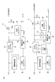
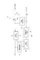
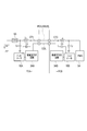
- the typical circuit block block diagram of the electric power supply apparatus which concerns on a basic technique.
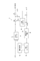
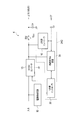
- A The typical circuit block block diagram of the electric power supply apparatus which concerns on 1st Embodiment
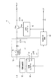
- b The typical circuit block block diagram of the electric power supply apparatus which concerns on the extended example of 1st Embodiment.
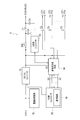
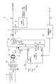
- the typical circuit block block diagram of the electric power supply apparatus which concerns on the modification 1 of 1st Embodiment.
- FIG. 1 It is a schematic diagram which shows the relationship between the output voltage and output current which are obtained using the electric power supply apparatus which concerns on 1st Embodiment, Comprising: (a) The example of the rectangular shape showing CVCC, (b) The inverted trapezoid " An example of a letter “F”, (c) an example of a letter “F” in an inverted triangle, (d) an example of a trapezoid, and (e) an example of a pentagon.
- the typical circuit block block diagram of the secondary side controller applied to the electric power supply apparatus which concerns on 1st Embodiment.
- the typical circuit block block diagram of the electric power supply apparatus which concerns on the modification 2 of 1st Embodiment.
- FIG. 2 is a schematic block configuration diagram of an insulated bidirectional circuit applicable to the power supply device according to the first embodiment (Configuration Example 1).
- the typical block block diagram of the insulated bidirectional circuit applicable to the electric power supply apparatus which concerns on 1st Embodiment (example 2 of a structure).
- the typical block block diagram of the insulated bidirectional circuit applicable to the electric power supply apparatus which concerns on 1st Embodiment (configuration example 3).
- the typical block block diagram of the insulated bidirectional circuit applicable to the electric power supply apparatus which concerns on 1st Embodiment (configuration example 4).
- the typical block block diagram of the insulated bidirectional circuit applicable to the electric power supply apparatus which concerns on 1st Embodiment (example 5 of a structure).
- the typical block block diagram of the insulated bidirectional circuit applicable to the electric power supply apparatus which concerns on 1st Embodiment (configuration example 6).
- the typical block block diagram of the insulated bidirectional circuit applicable to the electric power supply apparatus which concerns on 1st Embodiment (example 7 of a structure).
- the typical block block diagram of the insulated bidirectional circuit and power output circuit which can be applied to the electric power supply apparatus which concerns on 1st Embodiment.
- the typical block block diagram of the insulated bidirectional circuit applicable to the electric power supply apparatus which concerns on 1st Embodiment (example 8 of a structure).
- the typical block block diagram of the insulated bidirectional circuit applicable to the electric power supply apparatus which concerns on 1st Embodiment (configuration example 10).
- the typical circuit block block diagram of the electric power supply apparatus which concerns on the modification 6 of 1st Embodiment.
- the typical circuit block block diagram of the electric power supply apparatus which concerns on the modification 7 of 1st Embodiment.
- the typical circuit block block diagram of the electric power supply apparatus which concerns on 2nd Embodiment.
- the typical circuit block block diagram of the electric power supply apparatus which concerns on 3rd Embodiment.
- the typical circuit block block diagram of the electric power supply apparatus which concerns on 4th Embodiment.
- the typical circuit block block diagram of the electric power supply apparatus which concerns on 5th Embodiment.
- the typical circuit block block diagram of the electric power supply apparatus which concerns on 6th Embodiment.
- the typical circuit block block diagram of the electric power supply apparatus which concerns on 7th Embodiment.
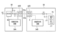
- FIG. 39 (A) The typical block diagram which connected between the electric power supply apparatuses which concern on 1st Embodiment via the receptacle plug cable, (b) The figure which shows the connection relation between two receptacles.
- A Schematic block configuration diagram for explaining a connection relationship between a power output circuit and a power input circuit applicable to the power supply device according to the first embodiment, (b) a schematic diagram corresponding to FIG. FIG.
- A Specific circuit configuration example of the power output circuit shown in FIG. 38 (b),
- 1 is a schematic circuit configuration diagram (configuration example 1) of a power output circuit applicable to the power supply apparatus according to the first embodiment.
- FIG. 1 is a schematic circuit configuration diagram (configuration example 1) of a power output circuit applicable to the power supply apparatus according to the first embodiment.
- the typical circuit block diagram of the power output circuit applicable to the electric power supply apparatus which concerns on 1st Embodiment structure example 3).
- the typical circuit block diagram of the power output circuit applicable to the electric power supply apparatus which concerns on 1st Embodiment structure example 4).
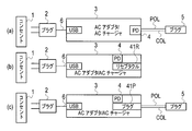
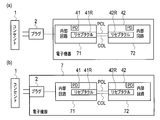
- a receptacle is provided in the / AC charger
- a plug built in the AC adapter / AC charger is connected to an external plug.
- C An example in which a plug built in the AC adapter / AC charger is connected to an external plug.
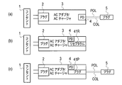
- An example in which a plug that can be connected to an outlet is built in an AC adapter / AC charger (a) an example in which a plurality of PDs in the AC adapter / AC charger and a plurality of external plugs are connected; (b) an AC adapter / An example in which a plurality of receptacles are provided in the AC charger, and (c) an example in which a plurality of plugs built in the AC adapter / AC charger and a plurality of external plugs are connected.
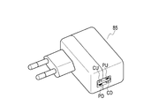
- 1 is a schematic bird's-eye view structure example of a power supply apparatus according to an embodiment applicable to an AC adapter, an AC charger, an electronic device, and a docking station equipped with a receptacle.
- 1 is a schematic bird's-eye view structure example of a power supply apparatus according to an embodiment applicable to an AC adapter, an AC charger, an electronic device, and a docking station equipped with a receptacle.
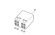
- 1 is a schematic bird's-eye view structural example of a power supply apparatus according to an embodiment applicable to an AC adapter, an AC charger, an electronic device, and a docking station equipped with a plurality of receptacles.
- FIG. 1 is a schematic bird's-eye view structure example of a power supply device according to an embodiment applicable to an AC adapter, an AC charger, an electronic device, and a docking station equipped with a plug.
- the typical block block diagram explaining the data communication between two PCs, and electric power supply in the electric power supply system which can apply the electric power supply apparatus which concerns on embodiment.
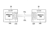
- the typical block block diagram explaining the data communication and electric power supply between two units in the electric power supply system which can apply the electric power supply apparatus which concerns on embodiment.
- the typical block block diagram of the electric power supply system which consists of AC adapter / AC charger smart phone incorporating the electric power supply apparatus which concerns on embodiment.
- the typical block block diagram of the electric power supply system which consists of two units incorporating the electric power supply apparatus which concerns on embodiment.
- the typical block block diagram which consists of another two units in the electric power supply system which can apply the electric power supply apparatus which concerns on embodiment.
- the 1st typical block block diagram of the electric power supply system which can apply the electric power supply apparatus which concerns on embodiment.
- the 2nd typical block block diagram of the electric power supply system which can apply the electric power supply apparatus which concerns on embodiment.
- the 3rd typical block block diagram of the electric power supply system which can apply the electric power supply apparatus which concerns on embodiment.
- the 4th typical block block diagram of the electric power supply system which can apply the electric power supply apparatus which concerns on embodiment.
- the typical block block diagram of the structure by which the controller is incorporated in CPU interface in the power supply system which can apply the power supply apparatus which concerns on embodiment.
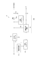
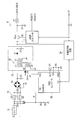
- the power supply device 4A As shown in FIG. 1, the power supply device 4A according to the basic technology is arranged between the input and the output, and is connected in series between the transformer 15, the diode D1, the capacitor C1, and the primary side inductance L1 of the transformer 15 between the ground potential.
- a DC / DC converter 13 composed of a connected MOS transistor Q1 and a resistor RS, a primary controller 30 that controls the MOS transistor Q1, and a primary controller 30 connected between the input and the primary controller 30.
- the connected error amplifier 21 for error compensation and the error amplifier 21 are connected to output information from the primary side controller 3.
- an isolation circuit 20 that feeds back to zero.
- the secondary side controller 16 may be connected to the output (VBUS) through an AC coupling capacitor.
- the power supply device 4A includes a switch SW that cuts off an output of the DC / DC converter 13 and a power line output (VBUS), and a switch SW and a power line output (VBUS). Is provided with a filter circuit (LF ⁇ CF). This switch SW can be turned on / off by the secondary controller 16.
- an AC signal is superimposed on the power line output (VBUS) and input from the outside.
- a control input signal is input from the power line output (VBUS) to the secondary controller 16, and the power information on the output side is primary through the error amplifier 21 and the insulation circuit 20. Is fed back to the side controller 30.
- the primary controller 30 controls ON / OFF of the MOS transistor Q1 and stabilizes the output voltage.
- the power supply device 4A according to the basic technology the amount of current conducted to the primary side inductance L1 is detected by the current sensing resistor RS, and the primary side controller 30 detects a current such as a primary side overcurrent. The amount is controlled. As a result, the power supply device 4A according to the basic technology has an output voltage value and output current value MAX variable function.
- the output voltage value and the outputable current amount (MAX value) variable function of the step-down DC / DC converter 13 by feedback control from the secondary controller 16 to the primary controller 30 Have Therefore, the load connected to the output (e.g., smart phones, laptop PC, tablet PC, etc.) in accordance with, a variable function of the relationship between the output voltage V o and the output current I o.
- the load connected to the output e.g., smart phones, laptop PC, tablet PC, etc.
- the inductance LF formed by the filter coil on the output side is a separation inductance.
- the input of the control input signal to the DC / DC converter 13 is separated from the output by the filter circuit configured by the inductance LF and the capacitor CF.
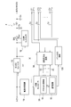
- FIG. 1 A schematic circuit block configuration of the power supply apparatus according to the first embodiment is expressed as shown in FIG.
- the power supply device 4 controls the DC / DC converter 13 disposed between the input and the VBUS output, and the input current of the DC / DC converter 13.
- a primary side controller 30 and an insulated bidirectional circuit 34 coupled to the control input, receiving a control input signal of the control input and feeding back to the primary side controller 30 are provided.
- the primary-side controller 30 controls the input current of the DC / DC converter 13 on the basis of the control input signal fed back from the insulating bidirectional circuit 34, and thereby the output voltage value of the DC / DC converter 13 and The outputable current amount (MAX value) is made variable.
- the power supply device 4 is arranged between the output of the DC / DC converter 13 and the VBUS output, and cuts off the output of the DC / DC converter 13. You may provide switch SW and the secondary side controller 16 which is connected to the insulation bidirectional circuit 34 and controls switch SW on / off.
- the power supply device 4 may include an AC coupling capacitor C C for coupling the control input and the insulating bidirectional circuit 34.
- control input and the insulating bidirectional circuit 34 may be connected directly without going through the coupling capacitor C C.
- the power supply device 4 according to the first embodiment may include a control terminal CT, and the control input may be coupled to the control terminal CT. Further, the control output signal of the power supply device 4 according to the first embodiment can be output to the external device via the control terminal CT.
- the insulated bidirectional circuit 34 can execute any one of frequency conversion, DC level conversion, and amplitude level conversion.
- the output of the DC / DC converter 13 and the power line output (VBUS) can be cut off by the switch SW.
- the switch SW can be on / off controlled by the secondary controller 16.
- the switch SW may include an insulated gate field effect transistor (MOSFET: Metal-Oxide-Semiconductor-Field-Effect-Transistor).
- the power supply device 4 is connected between the input of the DC / DC converter 13 and the primary controller 30 as shown in FIG.
- a power supply circuit 10 for supplying power may be provided.
- the output voltage value of the step-down DC / DC converter 13 and the output possible current amount (MAX) are controlled by feedback control from the insulated bidirectional circuit 34 to the primary-side controller 30.
- Value) Variable function Therefore, the load connected to the output (e.g., smart phones, laptop PC, tablet PC, etc.) in accordance with, a variable function of the relationship between the output voltage V o and the output current I o.
- the power supply apparatus operates by feedback control different from that of the first embodiment. That is, the power supply apparatus according to the first extension example of the first embodiment includes a monitor circuit 22 that detects a primary side signal of the DC / DC converter 13 as shown in FIG.
- the side controller 30 controls the secondary side controller 16 via the insulated bidirectional circuit 34 based on the detection signal of the monitor circuit 22, thereby obtaining the output voltage value and the output possible current amount of the DC / DC converter 13. It is variable.
- the monitor circuit 22 can be composed of, for example, a circuit that detects the gate-drain voltage of the MOS transistor Q1 shown in FIG.
- the power supply apparatus according to the extension example 2 of the first embodiment operates by a feedback mechanism different from that of the first embodiment and the extension example 1.
- the power supply apparatus according to the extension example 2 of the first embodiment has an error connected between the output of the DC / DC converter 13 and the insulated bidirectional circuit 34 as shown in FIG.
- the primary-side controller 30 includes an amplifier 21 and receives a feedback signal received via the insulated bidirectional circuit 34 based on the detection signal of the error amplifier 21, and based on the feedback signal, the insulated bidirectional circuit
- the secondary side controller 16 via 34 the output voltage value of the DC / DC converter 13 and the output possible current amount are made variable.
- the configuration and feedback control of the extension examples 1 and 2 of the first embodiment can be similarly extended in the following modifications 1 to 7 of the first embodiment, and the same feedback control can be applied. is there. Further, the configurations of the extension examples 1 and 2 of the first embodiment can be similarly applied to the second to eighth embodiments, and the feedback control thereof can be similarly applied. In the following, repeated explanation is omitted.
- the power supply device 4 includes a DC / DC converter 13 disposed between the input and the VBUS output, and an input of the DC / DC converter 13.
- a primary-side controller 30 that controls the current; an isolation bidirectional circuit 34 that is coupled to the control input, receives a control input signal of the control input, and feeds back to the primary-side controller 30; and an output of the DC / DC converter 13
- a switch SW that is arranged between the VBUS output and cuts off the output of the DC / DC converter 13, a secondary controller 16 that is connected to the insulating bidirectional circuit 34 and controls the switch SW on and off, and the secondary controller 16 And an output capacitor C O arranged between the VBUS outputs.
- the primary-side controller 30 controls the input current of the DC / DC converter 13 on the basis of the control input signal fed back from the insulating bidirectional circuit 34, and thereby the output voltage value of the DC / DC converter 13 and
- the outputable current amount (MAX value) is made variable.
- the insulating bidirectional circuit 34 can further perform signal conversion / switching of the AC signal component of the VBUS output.
- the AC signal component of the VBUS output is coupled to the secondary controller 16 via an output capacitor C O connected between the VBUS output and the secondary controller 16 and can be transmitted to the isolated bidirectional circuit 34. .
- the power supply device 4 according to the first modification of the first embodiment may include a control terminal CT, and the control input may be coupled to the control terminal CT. Further, the control output signal of the power supply device 4 according to the first modification of the first embodiment can be output to the external device via the control terminal CT.
- control output signal of the power supply device 4 according to the first modification of the first embodiment is also transmitted to the external device via the output capacitor CO. Can be output.
- the inductance LF formed by the filter coil on the output side is a separation inductance.
- the filter circuit constituted by the inductance LF and the capacitor CF separates the control input signal from being input to the DC / DC converter 13 from the VBUS output.
- Other configurations are the same as those of the first embodiment.
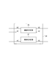
- the insulated bidirectional circuit 34 may include a plurality of insulated unidirectional circuits 35 and 37 as shown in FIG.
- the insulating bidirectional circuit 34 may include a first insulating unidirectional circuit 35 capable of DC coupling and AC coupling, and a second insulating unidirectional circuit 37 capable of AC coupling. .
- a capacitor, a photocoupler, a transformer or the like can be applied to the insulating unidirectional circuits 35 and 37. Further, a bidirectional transformer with an insulating driver, a bidirectional element, or the like may be applied depending on the application.
- the isolated unidirectional circuit 35 can transmit DC information and input AC information from the secondary side to the primary side, and the isolated unidirectional circuit 37 can output AC information from the primary side to the secondary side. Can be transmitted.
- the insulated bidirectional circuit 34 can be configured as a result.
- the output voltage value of the step-down DC / DC converter 13 and the output possible current amount (MAX) are controlled by feedback control from the insulated bidirectional circuit 34 to the primary-side controller 30.
- Value) Variable function Therefore, the load connected to the output (e.g., smart phones, laptop PC, tablet PC, etc.) in accordance with, a variable function of the relationship between the output voltage V o and the output current I o.
- the relationship between the output voltage V o obtained using the power supply device 4 according to the first embodiment and the output current I o is a rectangular shape as shown in FIG. 5A and shown in FIG. 5B.
- Various shapes such as a pentagonal shape can be adopted.
- the rectangular shape shown in FIG. 5A is an example of CVCC (Constant Voltage Constant Current).
- the output capacitor C O for extracting the AC signal that is superimposed on the power line output (VBUS) from the outside is provided as the secondary controller. 16 shows an example of connection between the power line output (VBUS).
- a separation inductance LF is required. That is, since it is necessary to separate the control input signal from being input to the DC / DC converter 13 from the power line output (VBUS), a filter circuit including the inductance LF and the capacitor CF is required.
- the separation inductance LF is not necessary. In this case, since the separation inductance LF can be reduced, the mounting area can be reduced, and the size and weight can be reduced.
- the secondary-side controller 16 may include a voltage / current control circuit 17 that controls the output voltage V o and the output current I o as shown in FIG. .
- the insulated bidirectional circuit 34 is coupled to a plurality of control inputs, and can perform signal conversion / switching of the control input signals of the plurality of control inputs. is there.
- the power supply device 4 includes a DC / DC converter 13 disposed between the input and the VBUS output, and an input of the DC / DC converter 13.
- a primary-side controller 30 that controls current and a plurality of control inputs are coupled to perform control conversion of the control input signals of the plurality of control inputs, and the signal-converted control input signal is fed back to the primary-side controller 30 And an insulating bidirectional circuit 34.
- the primary-side controller 30 controls the input current of the DC / DC converter 13 on the basis of the control input signal fed back from the insulating bidirectional circuit 34, and thereby the output voltage value of the DC / DC converter 13 and
- the outputable current amount (MAX value) is made variable.
- the DC / DC converter 13 corresponds to a plurality of VBUS outputs arranged in pairs with a plurality of control inputs. Output voltage can be supplied.
- the power supply device 4 includes a plurality of VBUS power output terminals PT1, PT2,..., PTn as shown in FIG. An output voltage can be supplied through a plurality of VBUS power output terminals PT1, PT2,.
- the primary controller 30 may include a communication circuit 19 that can perform code conversion. That is, the signal conversion of the control input signals of a plurality of control inputs performed in the insulated bidirectional circuit 34 may be performed in the communication circuit 19 in the primary side controller 30.
- the insulated bidirectional circuit 34 may have a configuration in which, for example, the insulated unidirectional circuits shown in FIG. 4 are arranged by the number of control inputs.
- the power supply device 4 may include an output capacitor CO that couples the secondary controller 16 and the VBUS output, as shown in FIG.
- the insulating bidirectional circuit 34 can further perform signal conversion / switching of the AC signal component of the VBUS output.
- the AC signal component of the VBUS output is coupled to the secondary controller 16 and the isolated bidirectional circuit 34 via an output capacitor C O connected between the VBUS output and the secondary controller 16.
- the power supply device 4 according to the second modification of the first embodiment includes a plurality of control terminals CT1, CT2,..., CTn, and a plurality of control inputs are a plurality of control terminals. It may be coupled to terminals CT1, CT2,. Moreover, the control output signal of the power supply device 4 according to the second modification of the first embodiment can be output to the external device via the plurality of control terminals CT1, CT2,. It may be provided with a coupling capacitor C C coupling a plurality of control terminals CT1 ⁇ CT2 ⁇ ... ⁇ CTn insulating bidirectional circuit 34. Alternatively, a plurality of control inputs and insulating bidirectional circuit 34 may be connected directly without going through the coupling capacitor C C.
- the power supply device 4 according to the second modification of the first embodiment is also connected to an external device through the output capacitor CO.
- the control output signal can be output.
- the power supply device 4 includes a switch SW that cuts off the output of the DC / DC converter 13 and the VBUS output, and a switch SW and a VBUS output.
- a filter circuit (LF ⁇ CF) disposed between the two may be provided.
- the inductance LF is omitted. Also good.
- Other configurations are the same as those of the first modification of the first embodiment.
- the power supply device 4 is connected to the primary-side controller 30 and outputs a plurality of VBUS outputs arranged in pairs with a plurality of control inputs.
- the power supply device 4 includes a plurality of VBUS power output terminals PT1, PT2, PT3, and a plurality of DC / DC converters 13 1 , 13 2 and 13 3 can supply an output voltage via a plurality of VBUS power output terminals PT1, PT2, and PT3.
- the power supply device 4 includes an AC coupling capacitor (not shown) coupled to a plurality of control inputs, and the insulated bidirectional circuit 34 is connected via the AC coupling capacitor. It may be coupled to a plurality of control inputs.
- the plurality of control inputs may be directly connected to the insulating bidirectional circuit 34. That is, a control input signal of a plurality of control inputs may be directly input to the insulated bidirectional circuit 34 as shown in FIG. 8 without using an AC coupling capacitor.
- the primary controller 30 may include a communication circuit 19 that can perform code conversion. That is, the signal conversion of the control input signals of a plurality of control inputs performed in the insulated bidirectional circuit 34 may be performed in the communication circuit 19 in the primary side controller 30.
- the insulated bidirectional circuit 34 may be configured by arranging, for example, the number of insulated unidirectional circuits shown in FIG. 4 corresponding to the number of control inputs.
- the power supply device 4 includes an output capacitor C O that combines the secondary controllers 16 1 , 16 2, and 16 3 and the VBUS output. May be provided.
- the insulating bidirectional circuit 34 can further perform signal conversion / switching of the AC signal component of the VBUS output.
- the AC signal component of the VBUS output passes through the output capacitor C O connected between the VBUS output and the secondary controller 16 1 , 16 2 , 16 3, and the secondary controller 16 1 , 16 2 , 16 3. • Coupled to isolated bidirectional circuit 34.
- Other configurations are the same as those of the second modification of the first embodiment.
- Modification 4 A schematic circuit block configuration of the power supply apparatus according to Modification 4 of the first embodiment is expressed as shown in FIG.
- the power supply device 4 includes a DC / DC converter 13 disposed between the input and the VBUS output, and an input of the DC / DC converter 13.
- a primary-side controller 30 that controls current and a plurality of control inputs are coupled to perform control conversion of the control input signals of the plurality of control inputs, and the signal-converted control input signal is fed back to the primary-side controller 30 And an insulating bidirectional circuit 34.
- the primary-side controller 30 controls the input current of the DC / DC converter 13 on the basis of the control input signal fed back from the insulating bidirectional circuit 34, and thereby the output voltage value of the DC / DC converter 13 and
- the outputable current amount (MAX value) is made variable.
- the power supply device 4 is connected to the primary-side controller 30 and outputs a plurality of VBUS outputs arranged in pairs with a plurality of control inputs. And a power output circuit 130 for supplying an output voltage.
- the power output circuit 130 may include a plurality of DC / DC converters.
- the power supply device 4 includes a plurality of VBUS power output terminals PT1, PT2,..., PTn, and the power output circuit 130 includes a plurality of power output circuits 130.
- the output voltage can be supplied through the VBUS power output terminals PT1, PT2,.
- the power supply device 4 includes an AC coupling capacitor (not shown) coupled to a plurality of control inputs, and the insulated bidirectional circuit 34 is connected via the AC coupling capacitor. It may be coupled to a plurality of control inputs.
- the plurality of control inputs may be directly connected to the insulating bidirectional circuit 34.
- a plurality of control input control input signals may be directly input to the insulating bidirectional circuit 34 without using an AC coupling capacitor.
- the power supply device 4 is arranged between the output of the DC / DC converter 13 and the VBUS output as shown in FIG.
- a switch SW that shuts off the output and a secondary-side controller 16 that is connected to the insulating bidirectional circuit 34 and controls the switch SW on and off may be provided.
- an output capacitor C O that couples the secondary side controller 16 and the VBUS output may be provided.
- the primary-side controller 30 may include a protocol conversion unit 18 that can perform frequency conversion and a communication circuit 19 that can perform code conversion. That is, the signal conversion of the control input signals of the plurality of control inputs performed in the insulated bidirectional circuit 34 may be performed in the protocol conversion unit 18 and the communication circuit 19 in the primary side controller 30.
- the insulated bidirectional circuit 34 may be configured by arranging, for example, the number of insulated unidirectional circuits shown in FIG. 4 corresponding to the number of control inputs.
- the primary-side controller 30 can further perform signal conversion / switching of the AC signal component of the VBUS output.
- the AC signal component of the VBUS output is coupled to the secondary controller 16, the isolated bidirectional circuit 34, and the primary controller 30 via an output capacitor C O connected between the VBUS output and the secondary controller 16. Is done.
- the power supply device 4 according to the fourth modification of the first embodiment includes a plurality of control terminals CT1, CT2,..., CTn, and a plurality of control inputs are a plurality of control terminals. It may be coupled to terminals CT1, CT2,. Further, the control output signal of the power supply device 4 according to the fourth modification of the first embodiment can be output to the external device via the plurality of control terminals CT1, CT2,. It may be provided with a coupling capacitor C C coupling a plurality of control terminals CT1 ⁇ CT2 ⁇ ... ⁇ CTn insulating bidirectional circuit 34. Alternatively, a plurality of control inputs and insulating bidirectional circuit 34 may be connected directly without going through the coupling capacitor C C.
- the power supply device 4 according to the second modification of the first embodiment is also connected to an external device through the output capacitor CO.
- the control output signal can be output.
- the power supply device 4 includes a switch SW that cuts off the output of the DC / DC converter 13 and the VBUS output, and a switch SW and a VBUS output.
- a filter circuit (LF ⁇ CF) disposed between the two may be provided.
- the inductance LF is omitted. Also good.
- Other configurations are the same as those of the second modification of the first embodiment.
- the power supply devices According to the power supply devices according to Modifications 2 to 4 of the first embodiment, switching to a plurality of devices is possible, the number of parts is reduced, the size and cost are reduced, and the output voltage value and It is possible to provide a power supply device that can control the amount of current that can be output (MAX value).
- FIG. 1 A schematic block configuration of the insulating bidirectional circuit 34 applicable to the power supply apparatus according to the first embodiment is expressed as shown in FIG.
- the insulated bidirectional circuit 34 is connected to the primary-side controller 30 as shown in FIG. 10, and includes a protocol conversion unit 18 that performs frequency conversion, and a protocol conversion unit. 18 and a control input, and a communication circuit 19 that performs code conversion may be provided.
- control inputs at the plurality of control terminals CT1, CT2,..., CTn are encoded and modulated by the communication circuit 19, and at the protocol converter 18, for example, the frequency f1 ⁇
- the frequency is converted to f2 and input to the primary controller 30.
- control output signal of the power supply device 4 can be output to an external device via the plurality of control terminals CT1, CT2,. That is, the control signal from the primary-side controller 30 is also frequency-converted by the protocol converter 18 from, for example, the frequency f2 ⁇ f1, and is encoded and modulated by the communication circuit 19, so that a plurality of control terminals CT1, CT2,. Can be output to CTn.
- the AC signal component superimposed on the VBUS output is frequency-converted by the protocol converter 18 via the output capacitor C O ⁇ secondary controller 16, for example, from the frequency f 1 to f 2, and is encoded by the communication circuit 19. Modulated and input to the primary controller 30.
- the control signal from the primary controller 30 is also frequency-converted by the protocol converter 18 from, for example, the frequency f2 ⁇ f1, and is encoded and modulated by the communication circuit 19, and the secondary controller 16 and the output capacitor C O. Can be output to the VBUS output.
- the control output signal of the power supply device 4 according to the first embodiment can be output to the external device even through the VBUS output.
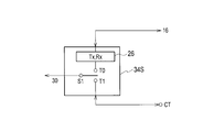
- FIG. 1 A schematic block configuration example 1 of the insulated bidirectional circuit 34S applicable to the power supply apparatus according to the first embodiment is expressed as shown in FIG.
- the insulated bidirectional circuit 34S is connected to the primary controller 30 and input to the secondary controller 16 and the control terminal CT as shown in FIG.
- a changeover switch (S1, T0, T1) that switches between control inputs may be provided.
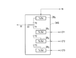
- the insulated bidirectional circuit 34S is connected to the transceiver 26 connected to the secondary controller 16 and the primary controller 30 as shown in FIG. There may be provided a changeover switch (S1, T0, T1) for switching between the transceiver 26 and the control input inputted to the control terminal CT.
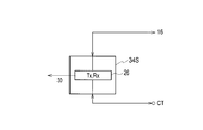
- the insulated bidirectional circuit 34S is connected to the primary controller 30 and input to the secondary controller 16 and the control terminal CT as shown in FIG. You may provide the transmitter / receiver 26 which switches between inputs.
- the transmitter / receiver 26 can perform transmission / reception signal conversion / switching between the secondary-side controller 16 and a control input input to the control terminal CT.
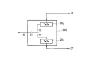
- FIG. 4 A schematic block configuration example 4 of the insulated bidirectional circuit 34S applicable to the power supply apparatus according to the first embodiment is expressed as shown in FIG.
- a power supply device according to the first embodiment, the insulating bidirectional circuit 34S, as shown in FIG. 14, a first transceiver 26 0 which is connected to the secondary-side controller 16, is input to the control terminal CT a second transceiver 261 that is connected to the control input that is connected to the primary side controller 30, the changeover switch (S1 ⁇ T0 ⁇ T1 for switching between the first transceiver 26 0 and the second transceiver 26 1 ).
- the first transceiver 26 0 second transceiver 26 1 is provided with the same configuration.
- FIG. 5 A schematic block configuration example 5 of the insulated bidirectional circuit 34S applicable to the power supply apparatus according to the first embodiment is expressed as shown in FIG.
- a power supply device according to the first embodiment, the insulating bidirectional circuit 34S, as shown in FIG. 15, a first transceiver 26 0 which is connected to the secondary-side controller 16, is input to the control terminal CT a second transceiver 261 that is connected to the control input that is connected to the primary side controller 30, the changeover switch (S1 ⁇ T0 ⁇ T1 for switching between the first transceiver 26 0 and the second transceiver 26 1 ).
- the first transceiver 26 0 second transceiver 26 1 is provided with a different configuration from each other.
- FIG. 6 A schematic block configuration example 6 of the insulated bidirectional circuit 34S applicable to the power supply apparatus according to the first embodiment is expressed as shown in FIG.
- a power supply device according to the first embodiment, the insulating bidirectional circuit 34S, as shown in FIG. 16, a first transceiver 26 0 which is connected to the secondary-side controller 16, CT1 ⁇ a plurality of control terminals a plurality of second transceiver 26 1, 26 2, 26 3 which are connected to the control input inputted to the CT2-CT3, connected to the primary side controller 30, the first transceiver 26 0 and a plurality of second A changeover switch (S1, T0, T1) for switching between the transceivers 26 1 , 26 2, and 26 3 may be provided.
- the second transceiver 26 1, 26 2, 26 3 multiple has a same configuration, the first transceiver 26 0 second transceiver 26 1, 26 2, 26 3 is provided with a different configuration from each other May be.
- FIG. 7 A schematic block configuration example 7 of the insulated bidirectional circuit 34S applicable to the power supply apparatus according to the first embodiment is expressed as shown in FIG.
- the insulating bidirectional circuit 34S is connected to the primary-side controller 30 and connected to the secondary-side controller 16 and a plurality of control terminals CT1, CT2,.
- a switch (S1, T0, T1, T2, T3,..., Tn) that switches between a plurality of control inputs input to CT3,.
- the primary side controller 30 is connected to the plurality of VBUS outputs arranged in pairs with the plurality of control inputs.
- a power output circuit 130 for supplying an output voltage may be provided.
- a plurality of VBUS power output terminals PT1, PT2,..., PTn arranged in pairs with a plurality of control terminals CT1, CT2, CT3,.
- An output voltage can be supplied through a plurality of VBUS power output terminals PT1, PT2,.
- 19 is a schematic block configuration example 8 of the insulated bidirectional circuit 34S applicable to the power supply apparatus according to the first embodiment.
- the power supply apparatus is connected to the primary-side controller 30 and supplies an output voltage to a plurality of VBUS outputs arranged in pairs with a plurality of control inputs.
- the insulated bidirectional circuit 34S may include a changeover switch (S1, T0, T1, T2, T3,..., Tn) for switching a plurality of control inputs.
- a plurality of control inputs are coupled to a plurality of control terminals CT1, CT2,..., CTn, and external devices are connected via the plurality of control terminals CT1, CT2,.
- the control output signal of the power supply device 4 according to the first embodiment can be output.
- the power output circuit 130 can supply an output voltage via a plurality of VBUS power output terminals PT1, PT2,.
- FIG. 9 A schematic block configuration example 9 of the insulating bidirectional circuit 34 applicable to the power supply apparatus according to the first embodiment is expressed as shown in FIG.
- the power supply apparatus is connected to the primary controller 30 and supplies output voltages to a plurality of VBUS outputs arranged in pairs with a plurality of control inputs.
- the insulated bidirectional circuit 34 may include a port selector 116 that switches a plurality of control inputs.
- a plurality of control inputs are coupled to a plurality of control terminals CT1, CT2,..., CTn, and external devices are connected via the plurality of control terminals CT1, CT2,.
- the control output signal of the power supply device 4 according to the first embodiment can be output.
- the power output circuit 130 can supply an output voltage via a plurality of VBUS power output terminals PT1, PT2,.
- FIG. 21A a configuration example of the port selector 116 is represented as shown in FIG. 21A, and another configuration example is represented as shown in FIG.
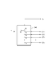
- the port selector 116 may include a CPU 125 and a switch SW that is connected to the CPU 125 and switches a plurality of control terminals CT1, CT2,.
- the port selector 116 may include a CPU 125 connected to a plurality of control terminals CT1, CT2,. That is, in the example shown in FIG. 21B, the CPU 125 itself may be provided with a switch function for switching a plurality of control terminals CT1, CT2,.
- FIG. 10 A schematic block configuration example 10 of the insulated bidirectional circuit 34 applicable to the power supply apparatus according to the first embodiment is expressed as shown in FIG.
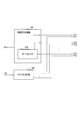
- the insulated bidirectional circuit 34 may include a plurality of port selectors 116 1 and 116 2 as shown in FIG.
- control input terminals CT 1 and CT 2 are connected to the port selector 116 1
- control input terminals CT 3 and CT 4 are connected to the port selector 116 2 .
- the power supply device is connected to the primary controller 30 and arranged in pairs with a plurality of control inputs.
- a power output circuit for supplying an output voltage to the VBUS output may be provided.
- the port selectors 116 1 and 116 2 may include a CPU and a switch that is connected to the CPU and switches a plurality of control terminals, as in the configuration example 9 of FIGS. 21A and 21B. Alternatively, a CPU connected to a plurality of control terminals may be provided.
- the power supply device 4 may include an insulated bidirectional circuit 34E in which the secondary controller 16 is built. That is, the insulated bidirectional circuit 34 and the secondary side controller 16 may be integrally formed as shown in FIG. Other configurations are the same as those of the first embodiment.
- the power supply device 4 may include an insulated bidirectional circuit 34P in which the primary controller 30 is built, as illustrated in FIG. That is, the primary controller 30 and the insulated bidirectional circuit 34 may be integrally formed as shown in FIG. Other configurations are the same as those of the first embodiment.
- the power supply device 4 includes an insulated bidirectional circuit 34G in which the secondary controller 16 and the primary controller 30 are built, as shown in FIG. May be. That is, the secondary side controller 16, the primary side controller 30, and the insulating bidirectional circuit 34 may be integrally formed as shown in FIG. Other configurations are the same as those of the first embodiment.
- the first embodiment and its modification it is possible to provide a power supply apparatus that can reduce the mounting space, can be downsized and reduced in cost, and can control the output voltage value and the outputable current amount (MAX value). Can do.
- the power supply device 4 according to the second embodiment is represented as shown in FIG.
- the DC / DC converter 13 includes a diode rectification type as shown in FIG.
- the DC / DC converter 13 is connected in series between the transformer 15, the primary inductance L1 of the transformer 15, and the ground potential, as shown in FIG.
- a capacitor C1 a capacitor
- the power supply device 4 controls the DC / DC converter 13 disposed between the input and the VBUS output, and the input current of the DC / DC converter 13.
- a primary side controller 30 and an insulated bidirectional circuit 34 coupled to the control input, receiving a control input signal of the control input and feeding back to the primary side controller 30 are provided.
- the primary-side controller 30 controls the input current of the DC / DC converter 13 on the basis of the control input signal fed back from the insulating bidirectional circuit 34, and thereby the output voltage value of the DC / DC converter 13 and The outputable current amount (MAX value) is made variable.
- the power supply device 4 is arranged between the output of the DC / DC converter 13 and the VBUS output, and cuts off the output of the DC / DC converter 13.
- a MOS switch Q SW and a secondary controller 16 connected to the insulating bidirectional circuit 34 and controlling the on / off of the MOS switch Q SW may be provided.
- the power supply device 4 according to the second embodiment may include a control terminal CT, and the control input may be coupled to the control terminal CT. Further, the control output signal of the power supply device 4 according to the second embodiment can be output to the external device via the control terminal CT.
- Other configurations are the same as those of the first embodiment.
- the second embodiment it is possible to provide a power supply device that can reduce the mounting space, reduce the size and cost, and can control the output voltage value and the outputable current amount (MAX value).
- the DC / DC converter 13 includes a synchronous rectification type as shown in FIG.
- the DC / DC converter 13 is connected in series between the transformer 15, the primary side inductance L1 of the transformer 15, and the ground potential as shown in FIG.
- a capacitor C1 a capacitor
- the power supply device 4 controls the DC / DC converter 13 disposed between the input and the VBUS output, and the input current of the DC / DC converter 13.
- a primary side controller 30 and an insulated bidirectional circuit 34 coupled to the control input and performing signal conversion of the control input signal of the control input and feeding back the signal-converted control input signal to the primary side controller 30 Prepare.
- the primary-side controller 30 controls the input current of the DC / DC converter 13 on the basis of the control input signal fed back from the insulating bidirectional circuit 34, and thereby the output voltage value of the DC / DC converter 13 and
- the outputable current amount (MAX value) is made variable.
- the power supply device 4 is arranged between the output of the DC / DC converter 13 and the VBUS output, and cuts off the output of the DC / DC converter 13.
- a MOS switch Q SW and a secondary controller 16 connected to the insulating bidirectional circuit 34 and controlling the on / off of the MOS switch Q SW may be provided.
- the power supply device 4 according to the third embodiment may include a control terminal CT, and the control input may be coupled to the control terminal CT. Moreover, the control output signal of the power supply device 4 according to the third embodiment can be output to the external device via the control terminal CT.
- Other configurations are the same as those of the first embodiment.
- the power supply device 4 according to the third embodiment employs a synchronous rectification method instead of the diode rectification method for the DC / DC converter, compared to the second embodiment having the diode rectification method, DC / DC power conversion efficiency can be increased.
- the third embodiment it is possible to provide a power supply device that can reduce the mounting space, reduce the size and cost, and can control the output voltage value and the outputable current amount (MAX value).
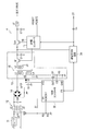
- the power supply device 4 As shown in FIG. 28, the power supply device 4 according to the fourth embodiment is connected to an AC input, instead of the power supply circuit 10 in the first embodiment, and includes a fuse 11, a choke coil 12, and a diode.
- An AC / DC converter including a rectifier bridge 14, capacitors C5, C6, and C3 is provided.
- the transformer 15 includes an auxiliary inductance L4 constituted by an auxiliary winding on the primary side of the transformer 15, and a diode D2 and a capacitor C4 connected in parallel to the auxiliary inductance L4.
- a DC voltage VCC is supplied to the side controller 30.
- the power supply device 4 includes a DC / DC converter 13 disposed between an input (DC output of an AC / DC converter) and a VBUS output, A primary side controller 30 that controls the input current of the DC converter 13 and a control input coupled to the control input, and performs signal conversion of the control input signal of the control input, and the signal converted control input signal is sent to the primary side controller 30 And an insulated bidirectional circuit 34 for feedback.
- the primary-side controller 30 controls the input current of the DC / DC converter 13 on the basis of the control input signal fed back from the insulating bidirectional circuit 34, and thereby the output voltage value of the DC / DC converter 13 and The outputable current amount (MAX value) is made variable.
- the power supply device 4 includes a secondary controller 16 disposed between the insulated bidirectional circuit 34 and the output of the DC / DC converter 13 as shown in FIG. May be.
- a control terminal CT may be provided, and a control input may be coupled to the control terminal CT.
- the control output signal of the power supply device 4 according to the fourth embodiment can be output to the external device via the control terminal CT.
- the secondary controller 16 describes PDDET1 and PDDET2 from the USB receptacle, but these may not be present.
- the DC / DC converter 13 is a diode rectification type. That is, the DC / DC converter 13 includes a transformer 15, a first MOS transistor Q 1 connected in series between the primary inductance L 1 of the transformer 15 and the ground potential, a current sensing resistor RS, and a secondary of the transformer 15. A diode D1 connected between the side inductance L2 and the output; and a first capacitor C1 connected between the output and the ground potential.
- the fourth embodiment it is possible to provide a power supply device that can be reduced in size and cost and that can control an output voltage value and an outputable current amount (MAX value).
- the power supply device 4 As shown in FIG. 29, the power supply device 4 according to the fifth embodiment is connected to an AC input instead of the power supply circuit 10 in the first embodiment, and includes a fuse 11, a choke coil 12, and a diode.
- An AC / DC converter including a rectifier bridge 14, capacitors C5, C6, and C3 is provided.
- the transformer 15 includes an auxiliary inductance L4 constituted by an auxiliary winding on the primary side of the transformer 15, and a diode D2 and a capacitor C4 connected in parallel to the auxiliary inductance L4.
- a DC voltage VCC is supplied to the side controller 30.
- the power supply device 4 includes a DC / DC converter 13 disposed between an input (DC output of an AC / DC converter) and a VBUS output, A primary side controller 30 that controls the input current of the DC converter 13 and a control input coupled to the control input, and performs signal conversion of the control input signal of the control input, and the signal converted control input signal is sent to the primary side controller 30 And an insulated bidirectional circuit 34 for feedback.
- the primary-side controller 30 controls the input current of the DC / DC converter 13 on the basis of the control input signal fed back from the insulating bidirectional circuit 34, and thereby the output voltage value of the DC / DC converter 13 and The outputable current amount (MAX value) is made variable.
- the power supply device 4 is arranged between the output of the DC / DC converter 13 and the VBUS output, and cuts off the output of the DC / DC converter 13.
- a MOS switch Q SW and a secondary controller 16 connected to the insulating bidirectional circuit 34 and controlling the on / off of the MOS switch Q SW may be provided.
- a control terminal CT may be provided, and a control input may be coupled to the control terminal CT.
- the control output signal of the power supply device 4 according to the fifth embodiment can be output to the external device via the control terminal CT.
- the secondary controller 16 describes PDDET1 and PDDET2 from the USB receptacle, but these may not be present.
- the DC / DC converter 13 is a diode rectification type. That is, the DC / DC converter 13 includes a transformer 15, a first MOS transistor Q 1 connected in series between the primary inductance L 1 of the transformer 15 and the ground potential, a current sensing resistor RS, and a secondary of the transformer 15. A diode D1 connected between the side inductance L2 and the output; and a first capacitor C1 connected between the output and the ground potential. Other configurations are the same as those of the second embodiment.
- the fifth embodiment it is possible to provide a power supply device that can be reduced in size and cost and that can control an output voltage value and an outputable current amount (MAX value).
- the power supply device 4 As shown in FIG. 30, the power supply device 4 according to the sixth embodiment is connected to an AC input instead of the power supply circuit 10 in the third embodiment, and includes a fuse 11, a choke coil 12, and a diode.
- An AC / DC converter including a rectifier bridge 14, capacitors C5, C6, and C3 is provided.
- the transformer 15 includes an auxiliary inductance L4 configured by an auxiliary winding on the primary side of the transformer 15, and a diode D2 and a capacitor C4 connected in parallel to the auxiliary inductance L4.
- a DC voltage VCC is supplied to the side controller 30.
- the power supply device 4 includes a DC / DC converter 13 disposed between an input (DC output of an AC / DC converter) and a VBUS output, A primary-side controller 30 that controls the input current of the DC converter 13 and a plurality of control inputs are coupled to perform a signal conversion of the control input signals of the plurality of control inputs, and the signal-converted control input signal is the primary And an isolated bidirectional circuit 34 that feeds back to the side controller 30.
- the primary-side controller 30 controls the input current of the DC / DC converter 13 on the basis of the control input signal fed back from the insulating bidirectional circuit 34, and thereby the output voltage value of the DC / DC converter 13 and
- the outputable current amount (MAX value) is made variable.
- the power supply device 4 includes a secondary-side controller 16 disposed between the insulated bidirectional circuit 34 and the output of the DC / DC converter 13 as shown in FIG. May be.
- a control terminal CT is provided, and a control input may be coupled to the control terminal CT.
- the control output signal of the power supply device 4 according to the sixth embodiment can be output to the external device via the control terminal CT.
- the secondary controller 16 describes PDDET1 and PDDET2 from the USB receptacle, but these may not be present.
- the DC / DC converter 13 is a synchronous rectification type. That is, the DC / DC converter 13 includes a transformer 15, a first MOS transistor Q 1 connected in series between the primary inductance L 1 of the transformer 15 and the ground potential, a current sensing resistor RS, and a secondary of the transformer 15. A second MOS transistor M1 connected between the side inductance L2 and the output; and a first capacitor C1 connected between the output and the ground potential. Other configurations are the same as those of the third embodiment.
- the power supply device 4 according to the sixth embodiment employs a synchronous rectification method instead of the diode rectification method for the DC / DC converter, the second, fourth, and fifth implementations having the diode rectification method are used. Compared with the embodiment, the DC / DC power conversion efficiency can be increased.
- the sixth embodiment it is possible to provide a power supply apparatus that can be reduced in size and cost and that can control an output voltage value and an outputable current amount (MAX value).
- the power supply device 4 according to the seventh embodiment is connected to an AC input instead of the power supply circuit 10 in the third embodiment, and includes a fuse 11, a choke coil 12, and a diode.
- the point provided with the AC / DC converter comprised from the rectification bridge 14, capacitor C5, C6, C3 etc. is the same as that of 6th Embodiment.
- an auxiliary inductance L4 configured by an auxiliary winding on the primary side of the transformer 15 and a diode D2 and a capacitor C4 connected in parallel to the auxiliary inductance L4 are provided.
- a DC voltage VCC is supplied to the side controller 30.
- the power supply device 4 includes a DC / DC converter 13 arranged between an input (DC output of an AC / DC converter) and a VBUS output, A primary side controller 30 that controls the input current of the DC converter 13 and a control input coupled to the control input, and performs signal conversion of the control input signal of the control input, and the signal converted control input signal is sent to the primary side controller 30 And an insulated bidirectional circuit 34 for feedback.
- the primary-side controller 30 controls the input current of the DC / DC converter 13 on the basis of the control input signal fed back from the insulating bidirectional circuit 34, and thereby the output voltage value of the DC / DC converter 13 and The outputable current amount (MAX value) is made variable.
- the power supply device 4 is arranged between the output of the DC / DC converter 13 and the VBUS output, and cuts off the output of the DC / DC converter 13.
- a MOS switch Q SW and a secondary controller 16 connected to the insulating bidirectional circuit 34 and controlling the on / off of the MOS switch Q SW may be provided.
- a control terminal CT may be provided, and a control input may be coupled to the control terminal CT.
- the control output signal of the power supply device 4 according to the fifth embodiment can be output to the external device via the control terminal CT.
- the secondary controller 16 includes PDDET1 and PDDET2, but these may be omitted.
- the DC / DC converter 13 is a synchronous rectification type. That is, as shown in FIG. 31, the DC / DC converter 13 includes a transformer 15, a first MOS transistor Q1 connected in series between the primary side inductance L1 of the transformer 15 and the ground potential, and a current sensing resistor RS. And a second MOS transistor M1 connected between the secondary inductance L2 of the transformer 15 and the output, and a first capacitor C1 connected between the output and the ground potential. Other configurations are the same as those of the sixth embodiment.
- the power supply device 4 according to the seventh embodiment employs a synchronous rectification method instead of the diode rectification method for the DC / DC converter, the second, fourth, and fifth implementations having the diode rectification method are employed. Compared with the embodiment, the DC / DC power conversion efficiency can be increased.
- the seventh embodiment it is possible to provide a power supply device that can be reduced in size and cost and that can control an output voltage value and an outputable current amount (MAX value).
- the power supply device 4 receives the DC / DC converter 13 disposed between the input and the output, and the input current of the DC / DC converter 13.
- a primary side controller 30 to be controlled and an insulated bidirectional circuit 34M connected to the control input and feeding back a control input signal of the control input to the primary side controller 30 are provided.
- the control input signal of the control input is input to the communication pin COM of the insulated bidirectional circuit 34M.
- the primary-side controller 30 controls the input current of the DC / DC converter 13 based on the control input signal fed back from the insulated bidirectional circuit 34M, whereby the output voltage value and output of the DC / DC converter 13 are controlled.
- the possible current amount (MAX value) is made variable.
- a control terminal CT may be provided, and a control input may be coupled to the control terminal CT. Further, the control output signal of the power supply device 4 according to the eighth embodiment can be output to the external device via the control terminal CT.
- the power supply device 4 includes an AC coupling capacitor C C coupled to the control input, and the insulating bidirectional circuit 34M is connected to the control input via the AC coupling capacitor C C. May be.
- the control input may be directly connected to the insulated bidirectional circuit 34M. That is, the control input signal of the control input not through the AC coupling capacitor C C in the insulating bidirectional circuit 34M, may be entered directly.
- a capacitor, a photocoupler, a transformer, or the like can be applied to the insulating bidirectional circuit 34M. Further, a bidirectional transformer with an insulating driver, a bidirectional element, or the like may be applied depending on the application.
- the secondary controller is excluded as shown in FIG.
- the power supply device 4 is connected to the output of the DC / DC converter 13 and cuts off the output voltage of the DC / DC converter 13 as shown in FIG. May be provided.
- the switch SW can cut off the output of the DC / DC converter 13 and the power line output (VBUS).
- This switch SW can be turned on / off by the primary controller 30 or the insulating bidirectional circuit 34M.
- the switch SW may include a MOS switch.
- the control input signal from the control input through the AC coupling capacitor C C is inputted to the insulated bidirectional circuit 34M, the control input signal, the power information on the output side Is fed back to the primary controller 30.
- the primary controller 30 controls the input current of the DC / DC converter 13 and stabilizes the output voltage.
- Other configurations are the same as those of the first embodiment.
- the power line output (VBUS) / AC superposition mode may be used in combination with the power line output (VBUS) / AC separation mode.
- the power supply device 4 includes a DC / DC converter 13 disposed between an input and an output, and a DC / DC converter 13 as shown in FIG.
- a primary-side controller 30 that controls the input current and an insulating bidirectional circuit 34C that is connected to the control input and feeds back a control input signal of the control input to the primary-side controller 30 are provided.
- the control input signal is input to the communication pin COM of the insulated bidirectional circuit 34C.
- the primary-side controller 30 controls the input current of the DC / DC converter 13 based on the control input signal fed back from the insulated bidirectional circuit 34C, so that the output voltage value and output of the DC / DC converter 13 are controlled.
- the possible current amount (MAX value) is made variable.
- a control terminal CT may be provided, and a control input may be coupled to the control terminal CT. Further, the control output signal of the power supply apparatus 4 according to the modification of the eighth embodiment can be output to the external device via the control terminal CT.
- the power supply device 4 according to a modification of the eighth embodiment, as shown in FIG. 19 (b), provided with an AC coupling capacitor C C coupled to the control input.
- AC coupling capacitor C C is incorporated in the insulating bidirectional circuit 34C.
- Insulating bidirectional circuit 34C is connected to the control input via an AC coupling capacitor C C has been built.
- the secondary controller is excluded as shown in FIG. 32 (b).
- a control input signal is input from the control input to the insulated bidirectional circuit 34C, and the control information including the power information on the output side is obtained by this control input signal.
- Feedback is provided to the primary controller 30.
- the primary controller 30 controls the input current of the DC / DC converter 13 and stabilizes the output voltage.
- Other configurations are the same as those in the eighth embodiment.
- the power line output (VBUS) / AC superposition mode may be used together with the power line output (VBUS) / AC separation mode.
- no filter coil is required on the output side, the mounting space is reduced, the size and cost are reduced, and the output voltage value and the output possible current amount (MAX value) are controlled.
- a possible power supply device can be provided.
- a schematic circuit block configuration example includes two n-channel MOSFETs Q n1 and Q n2 connected in series and discharges connected to both ends of the n-channel MOSFETs Q n1 and Q n2 connected in series.
- MOSFET Q D1 and Q D2 are provided.
- the gates of the two n-channel MOSFETs Q n1 and Q n2 connected in series are connected to the secondary-side controller 16 and controlled on / off by the secondary-side controller 16.
- the secondary controller 16 includes a voltage / current control circuit 17, and a control input signal is input to the communication pin COM of the secondary controller 16.
- the receptacles 41R and 42R each have a VBUS terminal, a CC1 terminal, a CC2 terminal, a D ⁇ terminal, a D + terminal, and a GND terminal, and connect the power supply apparatuses according to the first embodiment.
- the VBUS terminal is connected to a power line POL for two-way communication between devices.
- One is connected to a load (LOAD) and the other is connected to a variable power supply of about 5V to about 20V (MAX), for example.
- the variable power supply corresponds to the output voltage of the power supply apparatus according to the first embodiment.
- the GND terminal is a ground terminal.
- the CC1 terminal and CC2 terminal are communication terminals connected to a dedicated communication line COL for two-way communication between devices.
- the CC1 terminal is set so that a constant voltage can be supplied by the power supply VDD / impedance circuits Z1 and Z2.
- data BMC
- the CC1 terminal may be connected to a constant current source instead of supplying a constant voltage.
- each of the impedance circuits Z1 and Z2 can be configured by a parallel circuit of a current source and a resistor, for example, and either the current source or the resistor can be selected.
- a voltage control regulator (VCON) may be connected to one CC2 terminal, and a load (LOAD) may be connected to the other CC2 terminal.
- the D- terminal and D + terminal are serial data interface terminals that realize a flipping function.
- a schematic configuration inside the receptacle 41R (42R) applicable to the power supply apparatus according to the first embodiment is expressed as shown in FIG.
- VBUS, CC1, CC2, D ⁇ , D +, and GND terminals are arranged on both surfaces of the terminal arrangement board. For this reason, there is no distinction between front and back.
- FIG. 36 A schematic configuration in which the power supply apparatuses according to the first embodiment are connected via the receptacle 41R (42R) and the plug 41P (42P) is expressed as shown in FIG. As shown in FIG. 36, a plug 41P (42P) is inserted into the receptacle 41R (42R) so that power can be supplied through the power line POL, and data communication can be performed through the communication dedicated line COL.
- FIG. 41 A schematic configuration in which the power supply apparatuses according to the first embodiment are connected via the receptacles 41R, 42R, plug 2, and cable (POL / COL) is expressed as shown in FIG.
- the plug 2 corresponds to the plug 41P (42P) shown in FIG.
- the plug 2 has electrodes on one side corresponding to the shapes of the receptacles 41R and 42R shown in FIG. 35, and has VBUS, CC1, CC2, D ⁇ , D +, and GND terminals. Further, the plug 2 includes an electrode on the back surface side, and has GND, D +, D ⁇ , CC2, CC1, and VBUS terminals.
- the plug 2 can be called an improved USB plug, and the receptacle 41R (42R) can be called an improved USB receptacle.
- connection relationship between the two receptacles 41R and 42R is expressed as shown in FIG. As shown in FIG. 37 (b), the connection relationship between the two receptacles 41R and 42R is the normal connection N / normal connection N relationship between the receptacles 41R and 42R and the plugs 41P and 42P.
- connection relationships There are four possible connection relationships: a reverse connection R relationship, a reverse connection R / normal connection N relationship, and a reverse connection R / reverse connection R relationship.
- FIG. 1 A schematic block configuration for explaining the connection relationship between the power output circuit 130 and the load circuit 134 applicable to the power supply apparatus according to the first embodiment is expressed as shown in FIG.
- FIG. 1 A schematic circuit configuration corresponding to a) is expressed as shown in FIG.
- the load circuit 134 is disposed in an external device connected externally by connection between the receptacles 41R and 42R.
- the power output circuit 130 has a plurality of VBUS outputs, which are connected to the load circuit 134 via the power lines POL1, POL2, and PLO3.
- the power output circuit 130 includes a plurality of switches (SWP, P1, P2, and P3)
- the load circuit 134 includes a plurality of switches connected to the power lines POL1, POL2, and PLO3.
- SWP ⁇ P1 ⁇ P2 ⁇ P3 and connected to load 1, load 2 and load 3. Bidirectional connection between the power output circuit 130 and the load circuit 134 is possible.
- the power output circuit 130 includes a buffer 136 connected to the primary controller 30 and a plurality of switches (SWP1, SWP2, SWP3) connected to the output of the buffer 136.
- the plurality of switches (SWP1, SWP2, SWP3) can be constituted by bidirectional switches as shown in FIG. 39B, for example.
- a schematic circuit configuration example 1 of the power output circuit 130 applicable to the power supply apparatus according to the first embodiment is as shown in FIG. 27, in which the secondary side of the transformer 15 of the diode rectification type DC / DC converter 13 is used.
- a structure branched from the inductance L2 is provided. That is, the VBUS output VBUS1 is obtained from the output of the diode D11 and the capacitor C11 via the switch SW1 and the filter circuit LF1 and CF1, and the VBUS output VBUS2 is obtained from the output of the diode D12 and the capacitor C12 via the switch SW2 and the filter circuit LF2 and CF2.
- the VBUS output VBUS3 is obtained from the output of the diode D13 and the capacitor C13 via the switch SW3 and the filter circuit LF3 and CF3.
- a schematic circuit configuration example 2 of the power output circuit 130 applicable to the power supply apparatus according to the first embodiment includes a plurality of DC / DC converters 13 1 , 13 2 ,... 13 as shown in FIG. with n . That is, the VBUS output VBUS1 is obtained from the output of the DC / DC converter 13 1 via the switch SW1 and the filter circuit LF1 and CF1, and the VBUS is obtained from the output of the DC / DC converter 13 2 via the switch SW2 and the filter circuit LF2 and CF2. output VBUS2 is obtained, ..., VBUS output VBUSn from the output of the DC / DC converter 13 n via the switch SWn ⁇ filter circuit LFn ⁇ CFn is obtained.
- a schematic circuit configuration example 3 of the power output circuit 130 applicable to the power supply apparatus according to the first embodiment includes a diode rectification type DC / DC converter 13, a diode rectification type DC / DC A plurality of DC / DC converters 113 1 , 113 2 ,... 113 n connected to the output of the DC converter 13 are provided.
- VBUS output VBUS1 is obtained from the output of the DC / DC converter 113 1 via the switch SW1 ⁇ filter circuit LF1 ⁇ CF1, from the output of the DC / DC converter 113 2 via the switch SW2 ⁇ filter circuit LF2 ⁇ CF2 VBUS output VBUS2 is obtained, ..., VBUS output VBUSn from the output of the DC / DC converter 113 n via the switch SWn ⁇ filter circuit LFn ⁇ CFn is obtained.
- a schematic circuit configuration example 4 of the power output circuit 130 applicable to the power supply apparatus according to the first embodiment includes a diode rectification type DC / DC converter 13 and a DC / DC converter 13 as shown in FIG. And a plurality of MOS switches MS 11 , MS 12 , MS 21 , MS 22 , MS 31 , MS 32, which are connected to the output of the second switch and can be controlled in conduction state by the secondary controller 16. That, VBUS from the output of the plurality of MOS switches MS 11 ⁇ MS 12, MS 21 ⁇ MS 22, MS 31 ⁇ MS 32 output VBUS1, VBUS2, VBUS output VBUS3 is obtained.
- the power supply device 4 includes an AC adapter / AC charger. 3 can be built in.
- the AC adapter / AC charger 3 incorporating the power supply device (PD) 4 can be connected using a plug 2 and a cable that can be connected to the outlet 1, as shown in FIG. Further, it can be connected to a plug 5 arranged outside.
- the power supply device (PD) 4 and the plug 5 are connected by a power line POL and a communication dedicated line COL.
- a power line POL / communication dedicated line COL is directly connected to the power supply device (PD) 4.
- the AC adapter / AC charger 3 having the built-in power supply device (PD) 4 according to the embodiment can be connected using a plug 2 and a cable that can be connected to the outlet 1, as shown in FIG. 44 (b).
- a receptacle 41R may be provided.
- the AC adapter / AC charger 3 incorporating the power supply device (PD) 4 can be connected using a plug 2 and a cable that can be connected to the outlet 1 as shown in FIG. 44 (c).
- a plug 41P may be provided.
- the plug 41P can be connected to the plug 5 arranged outside.
- the plug 41P and the plug 5 are connected by a power line POL and a communication dedicated line COL.
- the AC adapter / AC charger 3 having the built-in power supply device (PD) 4 uses a plug 2 and a USB PD cable 6 that can be connected to an outlet 1 as shown in FIG. It is connectable and can be connected to the plug 5 arranged outside.
- the power supply device (PD) 4 and the plug 5 are connected by a power line POL and a communication dedicated line COL.
- a power line POL / communication dedicated line COL is directly connected to the power supply device (PD) 4.
- the AC adapter / AC charger 3 with the built-in power supply device (PD) 4 uses a plug 2 and a USB PD cable 6 that can be connected to an outlet 1 as shown in FIG. Connection is possible and a receptacle 41R may be provided.
- the AC adapter / AC charger 3 with the built-in power supply device (PD) 4 uses a plug 2 and a USB PD cable 6 that can be connected to an outlet 1 as shown in FIG.
- a plug 41P may be provided.
- the plug 41P can be connected to the plug 5 arranged outside.
- the plug 41P and the plug 5 are connected by a power line POL and a communication dedicated line COL.
- the plug 2 connectable to the outlet 1 is connected to the AC adapter / AC charger 3 incorporating the power supply device (PD) 4 according to the embodiment as shown in FIGS. 46 (a) to 46 (c). It may be built in.
- the AC adapter / AC charger 3 incorporating the power supply device (PD) 4 and the plug 2 according to the embodiment can be connected to the plug 5 arranged outside as shown in FIG.
- the power supply device (PD) 4 and the plug 5 are connected by a power line POL and a communication dedicated line COL.
- a power line POL / communication dedicated line COL is directly connected to the power supply device (PD) 4.
- the AC adapter / AC charger 3 incorporating the power supply device (PD) 4 and the plug 2 according to the embodiment may include a receptacle 41R as shown in FIG.
- the AC adapter / AC charger 3 incorporating the power supply device (PD) 4 and the plug 2 according to the embodiment may include a plug 41P as shown in FIG. 46 (c).
- the plug 41P can be connected to the plug 5 arranged outside.
- the plug 41P and the plug 5 are connected by a power line POL and a communication dedicated line COL.
- FIGS. 47A to 47C a plurality of power supply apparatuses according to the embodiment can be built in the AC adapter / AC charger 3. Moreover, the plug 2 which can be connected to the outlet 1 is incorporated.
- the AC adapter / AC charger 3 incorporating the power supply devices (PD) 41 and 42 and the plug 2 according to the plurality of embodiments includes a plurality of plugs 51 and 52 can be connected.
- the power supply devices (PD) 41, 42, plugs 51, 52 are connected by a power line POL and a communication dedicated line COL.
- a power line POL and a communication dedicated line COL are directly connected to the power supply devices (PD) 41 and 42.
- the AC adapter / AC charger 3 including the power supply devices 41 and 42 and the plug 2 according to the plurality of embodiments may include receptacles 41R and 42R as shown in FIG. 47 (b).
- the AC adapter / AC charger 3 including the power supply devices 41 and 42 and the plug 2 according to the plurality of embodiments may include plugs 41P and 42P as shown in FIG. 47 (c).
- the plugs 41P and 42P can be connected to plugs 51 and 52 arranged outside.
- the plugs 41P, 42P, and plugs 51 and 52 are connected by a power line POL and a communication dedicated line COL.
- the power supply apparatuses according to the first to eighth embodiments can be built in the electronic device 7 as shown in FIGS.
- Examples of electronic devices include monitors, external hard disk drives, set top boxes, laptop PCs, tablet PCs, smart phones, battery charger systems, personal computers, docking stations, displays, printers, vacuum cleaners, refrigerators, facsimiles, telephones,
- Various devices such as a car navigation system, a car computer, a television, glasses, a head mounted display, a fan, an air conditioner, a laser display, or a wall outlet can be applied.
- the plug 2 that can be connected to the outlet 1 and the electronic device 7 are connected using a cable, and internal circuits 71 and 72 that incorporate power supply devices 41 and 42 and receptacles 41R and 42R are provided inside the electronic device 7.
- An example provided is represented as shown in FIG.
- the plug 2 that can be connected to the outlet 1 is built in the electronic device 7 and the electronic device 7 includes the internal circuits 71 and 72 including the power supply devices 41 and 42 and the receptacles 41R and 42R is shown in FIG. It is expressed as shown in b).
- the receptacles 41R and 42R can be connected by a power line POL and a communication dedicated line COL.
- the plug 2 that can be connected to the outlet 1 is built in the electronic device 7 and the electronic device 7 includes the internal circuits 71 and 72 in which the power supply devices 41 and 42 and the receptacles 41R and 42R are built, one internal circuit 72
- An example having the receptacle 43R connected to the outside is represented as shown in FIG.
- the plug 2 that can be connected to the outlet 1 is built in the electronic device 7 and the electronic device 7 includes the internal circuits 71 and 72 that incorporate the power supply devices 41 and 42 and the receptacles 41R and 42R
- one internal An example having a plurality of receptacles 43R and 44R connected to the outside in the circuit 72 is expressed as shown in FIG.
- the receptacles 41R and 42R can be connected by the power line POL and the communication dedicated line COL.
- the power supply device 4 includes primary overpower protection circuits (OPP1) 81 and 83, primary overpower protection circuits ( The secondary overpower protection circuits (OPP2) 82 and 84 connected to the OPP1) 81 and 83 may be provided.
- Primary overpower protection circuits (OPP1) 81 and 83 are connected to a primary controller (not shown). Further, the primary side overpower protection circuits (OPP1) 81 and 83 may be incorporated in the primary side controller.
- the secondary overpower protection circuits (OPP2) 82 and 84 are connected to the insulating bidirectional circuit 34 and the secondary controller 16.
- the power information / communication control information in the receptacle 41R is transmitted from the insulated bidirectional circuit 34 to the secondary overpower protection circuits (OPP2) 82 and 84, and 2
- the secondary side overpower protection circuits (OPP2) 82 and 84 transmit the power information / communication control information to the primary side overpower protection circuits (OPP1) 81 and 83.
- Whether the power information / communication control information in the receptacle 41R exceeds the overcurrent detection set value is determined by either the primary side overpower protection circuit (OPP1) 81 or the secondary side overpower protection circuit (OPP2) 82. You may carry out.
- OPP1 primary side overpower protection circuit
- OPP2 secondary side overpower protection circuit
- the primary overpower protection circuits (OPP1) 81 and 83 are connected to the primary controller (illustrated).
- the overcurrent (overpower) protection control signal can be transmitted to (omitted) to switch the DC / DC converter 13 for power suppression.
- the power supply apparatus 4 includes overcurrent protection (OCP: Over Current Protection), overpower protection (OPP: Over Power Protection), overvoltage (OVP: Over Voltage Protection) protection, and overload protection (OLP: Various functions such as Over Load Protection and Over Temperature Protection (TSD: Thermal Shut Down) can be applied.
- OCP Over Current Protection
- OPP Over Power Protection
- OVP Over Voltage Protection
- OTP Over Voltage Protection
- the power supply device 4 includes, for example, a sensor (SENSOR) protection function that connects a sensor element to a primary controller (not shown) and performs protection according to the characteristics of the sensor element. May be.
- a sensor SENSOR
- a primary controller not shown
- the overcurrent (overpower) detection set value when the overcurrent (overpower) detection set value is changed, as described above, the power information / communication control information in the receptacle 41R is transmitted to the insulated bidirectional circuit 34 / secondary side.
- the overcurrent detection setting value is transmitted to the primary side overpower protection circuit (OPP1) 81/83 via the overpower protection circuit (OPP2) 82/84 and is connected to the receptacle 41R according to the target device (set). Can be changed to switch the power of the DC / DC converter 13.
- the power information / communication control information in the receptacle 41R is directly transmitted from the insulated bidirectional circuit 34 to the primary side overpower.
- the data may be transmitted to the protection circuits (OPP1) 81 and 83, and the set values may be directly changed in the primary side overpower protection circuits (OPP1) 81 and 83.
- POP1 primary side overpower protection circuit
- the supply power level is set according to the target device (set) connected to the receptacle 41R. It can be changed. As a result, destruction of the target device (set) in an abnormal state can be prevented.
- the connection target is a smart phone 160
- the 7-W power information / communication control information is transmitted from the secondary-side overpower protection circuit (OPP2) 82 to the primary-side overpower protection circuit (OPP1) 81.
- the overcurrent (overpower) detection set value UP is switched (SW) from 7 W to, for example, 10 W.
- SW overcurrent (overpower) detection set value UP
- the connection target is a laptop PC 140
- the 80-W power information / communication control information is transmitted from the secondary-side overpower protection circuit (OPP2) 84 to the primary-side overpower protection circuit (OPP1) 83.
- the overcurrent (overpower) detection set value UP is switched (SW) from 80 W to, for example, 100 W.
- SW overcurrent (overpower) detection set value UP
- the power supply device 85 As shown in FIG. 51, the power supply device 85 according to the embodiment applicable to an AC adapter, AC charger, electronic device, and docking station equipped with a receptacle can be connected to an outlet having an AC power supply of 100 V to 115 V, for example. Yes, and a plug connected to the power line POL / communication dedicated line COL can be inserted.
- An example of the plug structure is shown in FIG. 37 or FIG.
- the power line POL can be connected to either the upper power terminal PU or the lower power terminal PD of the receptacle, and the communication dedicated line COL can be connected to either the upper communication terminal CU or the lower communication terminal CD of the receptacle. It is.
- Power information can be transmitted to the power line POL, and communication control information can be transmitted to the communication dedicated line COL.
- a power supply device 85 applicable to an AC adapter, an AC charger, an electronic device, and a docking station equipped with the power supply device according to the embodiment includes a power terminal PU / PD and a communication terminal CU / CD. Any of these can be connected, so there is no need to select the top and bottom (front and back) of the corresponding plug, and it is easy to use.
- the upper power terminal PU / lower power terminal PD of the receptacle corresponds to the upper VBUS terminal / lower VBUS terminal of the receptacle 41R (42R) shown in FIGS.
- the upper communication terminal CU and the lower communication terminal CD of the receptacle correspond to the upper communication terminal CC1 (CC2) and the lower communication terminal CC1 (CC2) of the receptacle 41R (42R) shown in FIGS. ing.
- illustration is abbreviate
- the power supply device 86 according to the embodiment applicable to an AC adapter, AC charger, electronic device, and docking station equipped with a receptacle can be connected to, for example, an outlet having an AC power supply 230V as shown in FIG. Yes, and a plug connected to the power line POL / communication dedicated line COL can be inserted.
- An example of the plug structure is shown in FIG. 37 or FIG.
- a power supply device 87 according to an embodiment applicable to an AC adapter, an AC charger, an electronic device, and a docking station equipped with a receptacle is connected to an outlet having, for example, an AC power supply 100V to 115V. It is possible to insert a plurality of plugs connected to the power line POL / communication dedicated line COL. An example of the plug structure is shown in FIG. 37 or FIG.
- One or more insulating bidirectional circuits 34 can be incorporated in an AC adapter, an AC charger, an electronic device, and a docking station.
- the number of output outputs from the power supply devices 85, 86, 87 can be selected variously.
- the extraction number ratio may be 1: N, 1: 1, or N: 1.
- N is an integer of 2 or more. It can also be used in combination with a USBPD receptacle.
- a power supply device 88 according to an embodiment applicable to an AC adapter, an AC charger, an electronic device, and a docking station equipped with the plug 2 includes, for example, an outlet having an AC power source of 100V to 115V. Can be connected to an outlet having an AC power supply 230V. 44 (a), 44 (c), 45 (a), 45 (c), 46 (a), 46 (c), 47 (a), 47 (c). ). Further, the plug 2 may be applicable to a USB-PD. Therefore, in FIG. 54, the plug 2 can be referred to as an improved USB plug.
- the power source can be switched without changing the direction of the cable. For example, it is possible to charge a battery of a laptop PC from an external device and to supply power from the battery of the laptop PC to an external device (display, etc.) without replacing the cable.
- power transmission and half-duplex data communication can be realized between the two units via the power line POL / communication dedicated line COL.
- a DC power supply (DC output VBUS) and data communication are performed between the battery charger system and the laptop PC using a power line POL and a communication dedicated line COL. Can be used for transmission.
- the battery charger system / laptop PC is equipped with the power supply apparatus according to the embodiment.
- a DC power supply (DC output VBUS) and data communication can be performed between the smart phone and the laptop PC using the power line POL and the communication dedicated line COL. Can be used for transmission.
- the power supply apparatus according to the embodiment is mounted on the smart phone / laptop PC.
- FIG. 55 a schematic block configuration for explaining data communication and power supply between two personal computers PCA and PCB is expressed as shown in FIG.
- FIG. 55 illustration of the DC / DC converter is omitted, and the isolated bidirectional circuits 34A and 34B and the secondary side controllers 16A and 16B are shown.
- the personal computer PCA / PCB is equipped with the power supply apparatus according to the embodiment.
- the personal computers PCA and PCB are connected via a power line POL and a dedicated communication line COL.
- the dedicated communication line COL is connected between the control terminals CT1 and CT2.
- the control terminal CT1 is connected to the insulated bidirectional circuit 34A, and the control terminal CT2 is connected to the insulated bidirectional circuit 34B. Insulating bidirectional circuit 34A ⁇ 34B and the control terminal CT1 ⁇ CT2 between may be connected via an AC coupling capacitor C C.
- the personal computer PCA includes a battery E and a battery charger IC (CHG) 53 connected to the battery E, and the personal computer PCB includes a power management IC (PMIC: Power Management IC) 54. . Note that the inductances LF and CF constituting the filter circuit can be omitted.
- a cable is used for charging the battery E of the personal computer PCA from the personal computer PCB and feeding the personal computer PCB from the battery E of the personal computer PCA. It is feasible without.
- isolated bidirectional circuits 34A and 34B are connected to the communication dedicated line COL to realize, for example, half-duplex data communication between the personal computers PCA and PCB.
- the carrier frequency is, for example, about 23.2 MHz
- the FSK modulation / demodulation frequency is, for example, about 300 kbps.
- the bit error rate (BER) is about 1 ⁇ 10 ⁇ 6 , for example, and an LSI for BIST (built-in self test) may be incorporated.
- FIG. 1 a schematic block configuration for explaining data communication and power supply between the two units 56 and 58 is expressed as shown in FIG.
- the two units 56 and 58 are connected by a power line POL and a communication dedicated line COL.
- the power line POL and the communication dedicated line COL are plug-connected to the receptacles 41R and 42R built in the two units 56 and 58.
- the two units 56 and 58 are arbitrary electronic devices, and are mounted with the power supply device according to the embodiment.
- illustration of the DC / DC converter is omitted, and the isolated bidirectional circuits 34A and 34B are shown.
- AC coupling capacitor C C is omitted.
- FIG. 57 shows a schematic block configuration of a power supply system including the AC adapter / AC charger 3 and the smart phone 160 incorporating the power supply device according to the embodiment.
- the AC adapter / AC charger 3 and the smart phone 160 are connected by a power line POL and a communication dedicated line COL.
- the power line POL and the communication dedicated line COL are plug-connected to the receptacles 41R and 42R built in the AC adapter / AC charger 3 and the smart phone 160.
- the AC adapter / AC charger 3 / smartphone 160 includes the power supply device according to the embodiment.
- FIG. 57 illustration of the DC / DC converter is omitted, and the isolated bidirectional circuits 34A and 34B are shown.
- the AC adapter / AC charger 3 includes an AC / DC converter 60 and an insulated bidirectional circuit 34A.
- the smart phone 160 includes an insulating bidirectional circuit 34B, an embedded controller (EMBC) 64, a CPU 68, a PMIC 54, a battery 66, and a battery charger IC (CHG) 62.
- An AC coupling capacitor CC may be provided between the insulated bidirectional circuits 34A and 34B and the receptacles 41R and 42R. Note that the inductances LF and CF constituting the filter circuit can be omitted.
- charging the battery 66 of the smartphone 160 from the AC adapter / AC charger 3 and feeding the external device from the battery 66 of the smartphone 160 are cables. This can be realized without replacement.
- FIG. 1 A schematic block configuration of a power supply system including two units 56 and 58 incorporating a power supply device according to the embodiment is expressed as shown in FIG.
- the two units 56 and 58 are connected by a power line POL and a communication dedicated line COL.
- the power line POL and the communication dedicated line COL are plug-connected to the receptacles 41R and 42R built in the two units 56 and 58.
- the two units 56 and 58 are equipped with the power supply apparatus according to the embodiment.
- FIG. 58 illustration of the DC / DC converter is omitted, and the isolated bidirectional circuits 34A and 34B are shown.
- the unit 56 includes an AC / DC converter 60 and an insulated bidirectional circuit 34A
- the unit 58 includes an insulated bidirectional circuit 34B and a load 70.
- An AC coupling capacitor CC may be provided between the insulated bidirectional circuits 34A and 34B and the receptacles 41R and 42R.
- the load 70 can be configured by a CPU, a battery BAT, a controller CTR, and the like. Note that the inductances LF and CF constituting the filter circuit can be omitted.
- the power supply from the unit 56 to the unit 58 and the power supply from the unit 58 to the external device can be realized without replacing the cable.
- isolated bidirectional circuits 34A and 34B are connected to the communication dedicated line COL, and for example, half-duplex data communication is realized between the units 56 and 58.
- FIG. 58 a schematic block configuration including two units 56 and 58 different from the configuration of FIG. 58 is expressed as shown in FIG.
- the unit 56 includes a battery E, a CPU 68A, and an insulating bidirectional circuit 34A.
- the unit 58 includes a CPU 68B, an insulated bidirectional circuit 34B, and a load CL.
- the two units 56 and 58 are connected by a power line POL and a communication dedicated line COL.
- the power line POL and the communication dedicated line COL are plug-connected to receptacles 41R and 42R built in the two units 56 and 58 (not shown).
- the power line POL is connected between the battery E and the load CL, and the communication dedicated line COL is connected between the insulated bidirectional circuits 34A and 34B.
- the communication dedicated lines COL and the insulating bidirectional circuit 34A ⁇ 34B may be connected via an AC coupling capacitor C C, respectively.
- charging of the battery E from the unit 58 to the unit 56 and power feeding from the battery E of the unit 56 to the unit 58 can be realized without replacing the cable. It is. Also, for example, half-duplex data communication is realized between the units 56 and 58.
- a first power supply system 100 to which the power supply apparatus according to the embodiment can be applied globally includes a monitor 110 connected to an outlet via a plug, and an external connected to the monitor 110. It includes a hard disk drive 120, a set top box 180, a laptop PC 140, a tablet PC 150, and a smart phone 160.
- the monitor 110 may be a TV or a docking station.
- the power supply device 4 In each component, the power supply device 4 according to the embodiment is mounted. In FIG. 60, the DC / DC converter is not shown, and the insulated bidirectional circuit 34 is shown. Further, an AC coupling capacitor CC may be applied to the communication dedicated line COL.
- the power line POL is indicated by a thick solid line
- the communication dedicated line COL is indicated by a broken line.
- a power line POL may be used instead of the communication dedicated line COL indicated by a broken line.
- the communication dedicated line COL is connected to the insulated bidirectional circuit 34 via an AC coupling capacitor C C (not shown). On the other hand, it may be connected directly to the insulating bidirectional circuit 34 without passing through the AC coupling capacitor C C.
- the portion indicated by a circular broken line indicates that the power line POL cable and the communication dedicated line COL cable are separated.
- a USBPD cable can be used as the power line POL cable
- a communication dedicated cable (COM) can be used as the communication dedicated line COL cable.
- COM communication dedicated line
- a power line POL / communication dedicated line COL conversion built-in cable may be used.
- the monitor 110 has an AC / DC converter 60 and an insulated bidirectional circuit 34 mounted thereon
- the external hard disk drive 120 has a CPU + interface board 122 and an insulated bidirectional circuit 34 mounted thereon
- the set top box 180 has a CPU + interface.
- the board 132 and the insulated bidirectional circuit 34 are mounted.
- the laptop PC 140 includes an NVDC (Narrow Voltage DC / DC) charger 142, a CPU 148, a PCH (Platform Control Hub) 147, an EC (Embedded Controller) 146, and an insulated bidirectional circuit.
- the APC Application CPU
- the battery charger IC CHG
- the battery 157 the insulated bidirectional circuit 34
- the ACPU 166 and the USB battery charger are installed in the smartphone 160.
- Catcher IC 162, battery 172, the insulating bidirectional circuit 34 is mounted.
- the second power supply system 200 to which the power supply device according to the embodiment can be applied globally is connected to a USBPD adapter 230 connected to an outlet via a plug, and to the USBPD adapter 230.
- the laptop PC 140 may be a docking station.
- the power supply device 4 In each component, the power supply device 4 according to the embodiment is mounted. In FIG. 61, the DC / DC converter is not shown, and the insulated bidirectional circuit 34 is shown. Further, an AC coupling capacitor CC may be applied to the communication dedicated line COL.
- the USB PD adapter 230 is equipped with an AC / DC converter 60 and an insulating bidirectional circuit 34.
- the laptop PC 140 includes an NVDC charger 142, a CPU 148, a PCH 147, an EC 146, a battery 154, a DC / DC converter 159, an insulated bidirectional circuit 34 1 , 34 2 , and the monitor 110 has a PMIC 112, an insulated bidirectional circuit 34 Is installed.
- Other configurations are the same as those of the first power supply system 100 (FIG. 60).
- a third power supply system 300 to which the power supply device according to the embodiment can be applied globally includes a USBPD adapter / charger 310 connected to an outlet via a plug, and a USBPD adapter / charger. 310, an external hard disk drive 120, a monitor 110, a set-top box 180, a laptop PC 140, a tablet PC 150, and a smart phone 160 connected to 310.
- Each component is equipped with the power supply device 4 according to the embodiment.
- the DC / DC converter is not shown, and the insulated bidirectional circuit 34 is shown. Further, an AC coupling capacitor CC may be applied to the communication dedicated line COL.
- USB PD adapter / charger 310 Between the USB PD adapter / charger 310 and the external hard disk drive 120, the monitor 110, the set top box 180, the laptop PC 140, the tablet PC 150, and the smart phone 160, power transmission and communication data are performed using the power line POL and the communication dedicated line COL. Transmission is possible.
- the USB PD adapter / charger 310 is equipped with an AC / DC converter 60 and an insulated bidirectional circuit 34. Other configurations are the same as those of the first power supply system 100 (FIG. 60) and the second power supply system 200 (FIG. 61).
- a fourth power supply system 400 to which the power supply device according to the embodiment can be applied globally includes a high-function USB PD adapter / charger 330 connected to an outlet via a plug, and a high-function
- the external hard disk drive 120 connected to the USBPD adapter / charger 330, the monitor 110, the set top box 180, the laptop PC 140, the tablet PC 150, and the smart phone 160 are provided.
- Each component is mounted with the power supply device 4 according to the embodiment, but in FIG. 63, the DC / DC converter is not shown and the insulated bidirectional circuit 34 is shown. Further, an AC coupling capacitor CC may be applied to the communication dedicated line COL.
- the high function USBPD adapter / charger 330 is equipped with an AC / DC converter 60A and an insulated bidirectional circuit 34 incorporating a synchronous FET switching converter. Other configurations are the same as those of the third power supply system 300 (FIG. 62).
- FIG. 60 to 63 a schematic block configuration in which the insulated bidirectional circuit 34 is built in the CPU + interface board 122 (132) is expressed as shown in FIG. It is. That is, in the power supply systems 100 to 400 shown in FIGS. 60 to 63, the insulating bidirectional circuit 34 and the controller 16 may be built in the CPU + interface board 122 (132). In this case, power and communication data can be transmitted to the CPU + interface board 122 using the power line POL and the communication dedicated line COL.
- Such a chip in which the controller 16 is built in the CPU + interface board 122 (132) can be configured as an integrated chip with a CPU, DSP, or other controller including the controller.
- no filter coil is required on the output side, the mounting space is reduced, the size and cost are reduced, and the output voltage value and the output possible current amount (MAX value) are controlled.
- Possible power supply devices, AC adapters, AC chargers, electronic devices and power supply systems can be provided.
- the power supply device, AC adapter, AC charger, electronic device, and power supply system of this embodiment can be applied to home appliances, mobile devices, and the like.
- Monitor (TV, docking station) 116, 116 1 , 116 2 ... port selector 120 ... external hard disk drive (HDD) 122, 132 ... CPU + interface board 125 ... CPU 130 ... Power output circuit 134 ... Power input
- Receiver 180 ... Set top box 230 ... USBPD adapter CT, CT1, CT2, ..., CTn ... Control terminals PT1, PT2, ..., PTn ... VBUS power output terminal C C ... Coupling capacitor C O ... Output Capacitors
Landscapes
- Engineering & Computer Science (AREA)
- Power Engineering (AREA)
- Computer Networks & Wireless Communication (AREA)
- Signal Processing (AREA)
- Dc-Dc Converters (AREA)
- Cable Transmission Systems, Equalization Of Radio And Reduction Of Echo (AREA)
- Direct Current Feeding And Distribution (AREA)
Abstract
電力供給装置(4)は、入力とVBUS出力との間に配置されたDC/DCコンバータ(13)と、DC/DCコンバータ(13)の入力電流を制御する1次側コントローラ(30)と、制御入力に結合され、制御入力の制御入力信号を受信し、1次側コントローラ(30)にフィードバックする絶縁双方向回路(34)とを備える。1次側コントローラ(30)は、絶縁双方向回路(34)からフィードバックされた制御入力信号に基づいて、DC/DCコンバータ(13)の入力電流を制御することによって、DC/DCコンバータ(13)の出力電圧値および出力可能電流量を可変にする。実装スペースが削減され、小型化・低コスト化かつ出力電圧値および出力可能電流量(MAX値)を制御可能な電力給装置、ACアダプタ、ACチャージャ、電子機器および電力供給システムを提供する。
Description
本実施の形態は、電力供給装置、ACアダプタ、ACチャージャ、電子機器および電力供給システムに関する。
従来、電力供給を伴う通信規格に対応した端末装置と電力線搬送通信ネットワークとの間で相互通信可能な直流コンセントが提供されている。
データ線を用いた電力供給技術には、パワーオーバーイーサネット(PoE:Power Over Ethernet)技術やユニバーサルシリアルバス(USB:Universal Serial Bus)技術がある。
USB技術には、供給電力レベルに応じて、最大2.5WのUSB2.0、最大4.5WのUSB3.1、最大7.5Wのバッテリー充電規格BC1.2がある。
また、USBパワーデリバリー仕様は、従来のケーブルやコネクタとも互換性を備え、USB2.0やUSB3.1、USBバッテリー充電規格BC1.2とも共存する独立した規格である。この規格では、電圧5V~12V~20V、電流1.5A~2A~3A~5Aの範囲内で、充電電流・電圧を選択可能であり、10W・18W・36W・65W・最大100WまでUSB充電・給電可能である。
このような電力供給を実施する電源として、DC/DCコンバータがある。DC/DCコンバータには、ダイオード整流方式と同期整流方式がある。
ボブ・ダンスタン(Bob Dunstan)編, "USB Power Delivery Specification Revision 1.0", 2012年7月5日リリース, http://www.usb.org/developers/docs/
本実施の形態は、実装スペースが削減され、小型化・低コスト化かつ出力電圧値および出力可能電流量(MAX値)を制御可能な電力給装置、ACアダプタ、ACチャージャ、電子機器および電力供給システムを提供する。
本実施の形態の一態様によれば、入力とVBUS出力との間に配置されたDC/DCコンバータと、前記DC/DCコンバータの入力電流を制御する1次側コントローラと、制御入力に結合され、前記制御入力の制御入力信号を受信し、前記1次側コントローラにフィードバックする絶縁双方向回路と、前記DC/DCコンバータの出力と前記VBUS出力との間に配置され、前記DC/DCコンバータの出力を遮断するスイッチと、前記絶縁双方向回路に接続され、前記スイッチをオンオフ制御する2次側コントローラとを備え、前記1次側コントローラは、前記絶縁双方向回路からフィードバックされた前記制御入力信号に基づいて、前記入力電流を制御することによって、前記DC/DCコンバータの出力電圧値および出力可能電流量を可変にした電力供給装置が提供される。
本実施の形態の他の態様によれば、入力とVBUS出力との間に配置されたDC/DCコンバータと、前記DC/DCコンバータの入力電流を制御する1次側コントローラと、制御入力に結合され、前記制御入力の制御入力信号を受信し、前記1次側コントローラにフィードバックする絶縁双方向回路と、前記DC/DCコンバータの出力と前記VBUS出力との間に配置され、前記DC/DCコンバータの出力を遮断するスイッチと、前記絶縁双方向回路に接続され、前記スイッチをオンオフ制御する2次側コントローラと、前記DC/DCコンバータの1次側信号を検出するモニタ回路とを備え、前記1次側コントローラは、前記モニタ回路の検出信号に基いて、前記絶縁双方向回路を介して、前記2次側コントローラを制御することによって、前記DC/DCコンバータの出力電圧値および出力可能電流量を可変にした電力供給装置が提供される。
本実施の形態の他の態様によれば、入力とVBUS出力との間に配置されたDC/DCコンバータと、前記DC/DCコンバータの入力電流を制御する1次側コントローラと、制御入力に結合され、前記制御入力の制御入力信号を受信し、前記1次側コントローラにフィードバックする絶縁双方向回路と、前記DC/DCコンバータの出力と前記VBUS出力との間に配置され、前記DC/DCコンバータの出力を遮断するスイッチと、前記絶縁双方向回路に接続され、前記スイッチをオンオフ制御する2次側コントローラと、前記DC/DCコンバータの出力と前記絶縁双方向回路との間に接続されたエラーアンプとを備え、前記1次側コントローラは、前記エラーアンプの検出信号に基いて、前記絶縁双方向回路を介して受信したフィードバック信号を受信すると共に、前記フィードバック信号に基づいて、前記絶縁双方向回路を介して、前記2次側コントローラを制御することによって、前記DC/DCコンバータの出力電圧値および出力可能電流量を可変にした電力供給装置が提供される。
本実施の形態の他の態様によれば、上記の電力供給装置を搭載したACアダプタが提供される。
本実施の形態の他の態様によれば、上記の電力供給装置を搭載したACチャージャが提供される。
本実施の形態の他の態様によれば、上記の電力供給装置を搭載した電子機器が提供される。
本実施の形態の他の態様によれば、上記の電力供給装置を搭載した電力供給システムが提供される。
本実施の形態によれば、実装スペースが削減され、小型化・低コスト化かつ出力電圧値および出力可能電流量(MAX値)を制御可能な電力供給装置、ACアダプタ、ACチャージャ、電子機器および電力供給システムを提供することができる。
次に、図面を参照して、本実施の形態を説明する。以下の図面の記載において、同一又は類似の部分には同一又は類似の符号を付している。ただし、図面は模式的なものであり、厚みと平面寸法との関係、各層の厚みの比率等は現実のものとは異なることに留意すべきである。したがって、具体的な厚みや寸法は以下の説明を参酌して判断すべきものである。又、図面相互間においても互いの寸法の関係や比率が異なる部分が含まれていることはもちろんである。
又、以下に示す実施の形態は、技術的思想を具体化するための装置や方法を例示するものであって、構成部品の材質、形状、構造、配置等を下記のものに特定するものでない。この実施の形態は、特許請求の範囲において、種々の変更を加えることができる。
[基本技術]
基本技術に係る電力供給装置4Aは、図1に示すように、入力・出力間に配置され、トランス15・ダイオードD1・キャパシタC1およびトランス15の1次側インダクタンスL1に接地電位との間に直列接続されるMOSトランジスタQ1および抵抗RSから構成されるDC/DCコンバータ13と、MOSトランジスタQ1を制御する1次側コントローラ30と、入力と1次側コントローラ30間に接続され、1次側コントローラ30に電源を供給する電源供給回路10と、出力に接続され、出力電圧Voと出力電流Ioを制御可能な2次側コントローラ16と、DC/DCコンバータ13の出力と2次側コントローラ16に接続された誤差補償用のエラーアンプ21と、エラーアンプ21に接続され、出力情報を1次側コントローラ30にフィードバックする絶縁回路20とを備える。
基本技術に係る電力供給装置4Aは、図1に示すように、入力・出力間に配置され、トランス15・ダイオードD1・キャパシタC1およびトランス15の1次側インダクタンスL1に接地電位との間に直列接続されるMOSトランジスタQ1および抵抗RSから構成されるDC/DCコンバータ13と、MOSトランジスタQ1を制御する1次側コントローラ30と、入力と1次側コントローラ30間に接続され、1次側コントローラ30に電源を供給する電源供給回路10と、出力に接続され、出力電圧Voと出力電流Ioを制御可能な2次側コントローラ16と、DC/DCコンバータ13の出力と2次側コントローラ16に接続された誤差補償用のエラーアンプ21と、エラーアンプ21に接続され、出力情報を1次側コントローラ30にフィードバックする絶縁回路20とを備える。
また、2次側コントローラ16は、AC結合キャパシタを介して出力(VBUS)に接続されていても良い。
また、基本技術に係る電力供給装置4Aは、図1に示すように、DC/DCコンバータ13の出力と電力線出力(VBUS)を遮断するスイッチSWと、スイッチSWと電力線出力(VBUS)との間に配置されたフィルタ回路(LF・CF)を備える。このスイッチSWは、2次側コントローラ16によって、オン/オフ制御可能である。
基本技術に係る電力供給装置4Aにおいては、電力線出力(VBUS)に外部からAC信号が重畳されて入力される。
基本技術に係る電力供給装置4Aにおいては、電力線出力(VBUS)から制御入力信号が2次側コントローラ16に入力され、出力側の電力情報は、エラーアンプ21および絶縁回路20を介して、1次側コントローラ30にフィードバックされる。1次側コントローラ30は、MOSトランジスタQ1のON/OFFを制御し、出力電圧を安定化させる。
また、基本技術に係る電力供給装置4Aにおいては、電流センス用の抵抗RSにより、1次側インダクタンスL1に導通する電流量を検出し、1次側コントローラ30において、1次側過電流などの電流量を制御している。結果として、基本技術に係る電力供給装置4Aにおいては、出力電圧値および出力電流値MAX可変機能を有する。
基本技術に係る電力供給装置4Aにおいては、2次側コントローラ16から1次側コントローラ30へのフィードバック制御によって、降圧型DC/DCコンバータ13の出力電圧値および出力可能電流量(MAX値)可変機能を有する。このため、出力に接続される負荷(例えば、スマートホン、ラップトップPC、タブレットPCなど)に応じて、出力電圧Voと出力電流Ioとの関係に可変機能を有する。
出力側のフィルタコイルで形成されるインダクタンスLFは分離用のインダクタンスである。すなわち、インダクタンスLFとキャパシタCFにより構成されるフィルタ回路によって、出力から制御入力信号がDC/DCコンバータ13に入力されるのを分離している。
[第1の実施の形態]
第1の実施の形態に係る電力供給装置の模式的回路ブロック構成は、図2(a)に示すように表される。
第1の実施の形態に係る電力供給装置の模式的回路ブロック構成は、図2(a)に示すように表される。
第1の実施の形態に係る電力供給装置4は、図2に示すように、入力とVBUS出力との間に配置されたDC/DCコンバータ13と、DC/DCコンバータ13の入力電流を制御する1次側コントローラ30と、制御入力に結合され、制御入力の制御入力信号を受信し、1次側コントローラ30にフィードバックする絶縁双方向回路34とを備える。ここで、1次側コントローラ30は、絶縁双方向回路34からフィードバックされた制御入力信号に基づいて、DC/DCコンバータ13の入力電流を制御することによって、DC/DCコンバータ13の出力電圧値および出力可能電流量(MAX値)を可変にする。
また、第1の実施の形態に係る電力供給装置4は、図2に示すように、DC/DCコンバータ13の出力とVBUS出力との間に配置され、DC/DCコンバータ13の出力を遮断するスイッチSWと、絶縁双方向回路34に接続され、スイッチSWをオンオフ制御する2次側コントローラ16とを備えていても良い。
また、第1の実施の形態に係る電力供給装置4は、図2に示すように、絶縁双方向回路34と制御入力とを結合するAC結合キャパシタCCを備えていても良い。或いは、絶縁双方向回路34と制御入力は、結合キャパシタCCを介さずに直結されていても良い。
また、第1の実施の形態に係る電力供給装置4は、図2に示すように、制御端子CTを備え、制御入力は、制御端子CTに結合されていても良い。また、制御端子CTを介して、外部機器には、第1の実施の形態に係る電力供給装置4の制御出力信号が出力可能である。
また、第1の実施の形態に係る電力供給装置4において、絶縁双方向回路34は、周波数変換、直流レベル変換、振幅レベル変換のいずれかを実行可能である。
また、第1の実施の形態に係る電力供給装置4において、スイッチSWにより、DC/DCコンバータ13の出力と電力線出力(VBUS)を遮断することができる。スイッチSWは、2次側コントローラ16によって、オン/オフ制御可能である。スイッチSWは、絶縁ゲート型電界効果トランジスタ(MOSFET:Metal Oxide Semiconductor Field Effect Transistor)を備えていても良い。
また、第1の実施の形態に係る電力供給装置4は、図2に示すように、DC/DCコンバータ13の入力と、1次側コントローラ30との間に接続され、1次側コントローラ30に電源を供給する電源供給回路10を備えていても良い。
第1の実施の形態に係る電力供給装置4においては、絶縁双方向回路34から1次側コントローラ30へのフィードバック制御によって、降圧型DC/DCコンバータ13の出力電圧値および出力可能電流量(MAX値)可変機能を有する。このため、出力に接続される負荷(例えば、スマートホン、ラップトップPC、タブレットPCなど)に応じて、出力電圧Voと出力電流Ioとの関係に可変機能を有する。
(拡張例)
第1の実施の形態の拡張例に係る電力供給装置の模式的回路ブロック構成は、図2(b)に示すように表される。
第1の実施の形態の拡張例に係る電力供給装置の模式的回路ブロック構成は、図2(b)に示すように表される。
第1の実施の形態の拡張例1に係る電力供給装置は、第1の実施の形態とは異なるフィードバック制御により動作する。すなわち、第1の実施の形態の拡張例1に係る電力供給装置は、図2(b)に示すように、DC/DCコンバータ13の1次側信号を検出するモニタ回路22を備え、1次側コントローラ30は、モニタ回路22の検出信号に基いて、絶縁双方向回路34を介して、2次側コントローラ16を制御することによって、DC/DCコンバータ13の出力電圧値および出力可能電流量を可変にしている。
モニタ回路22は、例えば、図1に示されるMOSトランジスタQ1のゲート・ドレイン間電圧を検出する回路等で構成可能である。
第1の実施の形態の拡張例2に係る電力供給装置は、第1の実施の形態およびその拡張例1とは異なるフィードバック機構により動作する。すなわち、第1の実施の形態の拡張例2に係る電力供給装置は、図2(b)に示すように、DC/DCコンバータ13の出力と絶縁双方向回路34との間に接続されたエラーアンプ21を備え、1次側コントローラ30は、エラーアンプ21の検出信号に基いて、絶縁双方向回路34を介して受信したフィードバック信号を受信すると共に、このフィードバック信号に基づいて、絶縁双方向回路34を介して、2次側コントローラ16を制御することによって、DC/DCコンバータ13の出力電圧値および出力可能電流量を可変にしている。
第1の実施の形態の拡張例1・2の構成およびフィードバック制御は、以下の第1の実施の形態の変形例1~7においても同様に拡張可能であり、同様のフィードバック制御を適用可能である。また、第1の実施の形態の拡張例1・2の構成は、第2~第8の実施の形態においても同様に適用可能であり、またそのフィードバック制御も同様に適用可能である。以下において、重複説明は省略する。
(変形例1)
第1の実施の形態の変形例1に係る電力供給装置の模式的回路ブロック構成は、図3に示すように表される。
第1の実施の形態の変形例1に係る電力供給装置の模式的回路ブロック構成は、図3に示すように表される。
第1の実施の形態の変形例1に係る電力供給装置4は、図3に示すように、入力とVBUS出力との間に配置されたDC/DCコンバータ13と、DC/DCコンバータ13の入力電流を制御する1次側コントローラ30と、制御入力に結合され、制御入力の制御入力信号を受信し、1次側コントローラ30にフィードバックする絶縁双方向回路34と、DC/DCコンバータ13の出力とVBUS出力との間に配置され、DC/DCコンバータ13の出力を遮断するスイッチSWと、絶縁双方向回路34に接続され、スイッチSWをオンオフ制御する2次側コントローラ16と、2次側コントローラ16とVBUS出力の間に配置された出力キャパシタCOを備える。ここで、1次側コントローラ30は、絶縁双方向回路34からフィードバックされた制御入力信号に基づいて、DC/DCコンバータ13の入力電流を制御することによって、DC/DCコンバータ13の出力電圧値および出力可能電流量(MAX値)を可変にする。
絶縁双方向回路34は、さらに、VBUS出力のAC信号成分の信号変換・切替を実施可能である。VBUS出力のAC信号成分は、VBUS出力と2次側コントローラ16との間に接続された出力キャパシタCOを介して、2次側コントローラ16に結合され、絶縁双方向回路34に伝送可能である。
また、第1の実施の形態の変形例1に係る電力供給装置4は、図3に示すように、制御端子CTを備え、制御入力は、制御端子CTに結合されていても良い。また、制御端子CTを介して、外部機器には、第1の実施の形態の変形例1に係る電力供給装置4の制御出力信号が出力可能である。
また、第1の実施の形態に係る電力供給装置4において、出力キャパシタCOを介しても、外部機器には、第1の実施の形態の変形例1に係る電力供給装置4の制御出力信号が出力可能である。
出力側のフィルタコイルで形成されるインダクタンスLFは分離用のインダクタンスである。すなわち、インダクタンスLFとキャパシタCFにより構成されるフィルタ回路によって、VBUS出力から制御入力信号がDC/DCコンバータ13に入力されるのを分離している。その他の構成は、第1の実施の形態と同様である。
(絶縁双方向回路)
第1の実施の形態に係る電力供給装置に適用可能な絶縁双方向回路34の模式的ブロック構成は、図4に示すように表される。
第1の実施の形態に係る電力供給装置に適用可能な絶縁双方向回路34の模式的ブロック構成は、図4に示すように表される。
絶縁双方向回路34は、図4に示すように、複数の絶縁単方向回路35・37を備えていても良い。
また、絶縁双方向回路34は、図4に示すように、DC結合およびAC結合可能な第1絶縁単方向回路35と、AC結合可能な第2絶縁単方向回路37とを備えていても良い。
絶縁単方向回路35・37には、キャパシタ、フォトカプラ、トランスなどを適用可能である。また、用途に応じて、絶縁ドライバ付き双方向トランス、双方向素子などを適用しても良い。
ここで、絶縁単方向回路35は、DC情報および2次側から1次側への入力AC情報の伝送が可能であり、絶縁単方向回路37は1次側から2次側への出力AC情報の伝送が可能である。複数の絶縁単方向回路35・37を組み合わせることによって、結果として、絶縁双方向回路34を構成可能である。
第1の実施の形態に係る電力供給装置4においては、絶縁双方向回路34から1次側コントローラ30へのフィードバック制御によって、降圧型DC/DCコンバータ13の出力電圧値および出力可能電流量(MAX値)可変機能を有する。このため、出力に接続される負荷(例えば、スマートホン、ラップトップPC、タブレットPCなど)に応じて、出力電圧Voと出力電流Ioとの関係に可変機能を有する。
第1の実施の形態に係る電力供給装置4を用いて得られる出力電圧Voと出力電流Ioとの関係は、図5(a)に示すような矩形形状、図5(b)に示すような逆台形の「フ」の字形状、図5(c)に示すような逆三角形の「フ」の字形状、図5(d)に示すような台形形状、図5(e)に示すような五角形形状など、さまざまな形状を採用可能である。例えば、図5(a)に示す矩形形状は、CVCC(Constant Voltage Constant Current)の例である。
なお、第1の実施の形態の変形例1に係る電力供給装置4において、電力線出力(VBUS)に外部から重畳されて入力されるAC信号を抽出するための出力キャパシタCOが2次側コントローラ16・電力線出力(VBUS)間に接続される例が示されているが、この場合には、分離用のインダクタンスLFは必要となる。すなわち、電力線出力(VBUS)から制御入力信号がDC/DCコンバータ13に入力されるのを分離することが必要であるため、インダクタンスLFとキャパシタCFにより構成されるフィルタ回路が必要である。一方、第1の実施の形態に係る電力供給装置4においては、出力キャパシタCOを適用しないため、分離用のインダクタンスLFは不要となる。この場合、分離用のインダクタンスLFを削減可能であるため、実装面積を削減可能であり、小型化・軽量化を図ることができる。
第1の実施の形態に係る電力供給装置において、2次側コントローラ16は、図6に示すように、出力電圧Voと出力電流Ioを制御する電圧電流制御回路17を備えていても良い。
(変形例2)
第1の実施の形態の変形例2に係る電力供給装置の模式的回路ブロック構成は、図7に示すように表される。
第1の実施の形態の変形例2に係る電力供給装置の模式的回路ブロック構成は、図7に示すように表される。
第1の実施の形態の変形例2に係る電力供給装置4において、絶縁双方向回路34は、複数の制御入力に結合され、複数の制御入力の制御入力信号の信号変換・切替を実施可能である。
第1の実施の形態の変形例2に係る電力供給装置4は、図7に示すように、入力とVBUS出力との間に配置されたDC/DCコンバータ13と、DC/DCコンバータ13の入力電流を制御する1次側コントローラ30と、複数の制御入力に結合され、複数の制御入力の制御入力信号の信号変換を実施すると共に、信号変換された制御入力信号を1次側コントローラ30にフィードバックする絶縁双方向回路34とを備える。ここで、1次側コントローラ30は、絶縁双方向回路34からフィードバックされた制御入力信号に基づいて、DC/DCコンバータ13の入力電流を制御することによって、DC/DCコンバータ13の出力電圧値および出力可能電流量(MAX値)を可変にする。
また、第1の実施の形態の変形例2に係る電力供給装置4は、図7に示すように、DC/DCコンバータ13は、複数の制御入力と対に配置される複数のVBUS出力に対して出力電圧を供給可能である。
また、第1の実施の形態の変形例3に係る電力供給装置4は、図7に示すように、複数のVBUSパワー出力端子PT1・PT2・…・PTnを備え、DC/DCコンバータ13は、複数のVBUSパワー出力端子PT1・PT2・…・PTnを介して出力電圧を供給可能である。
また、1次側コントローラ30は、符号変換を実施可能な通信回路19を備えていても良い。すなわち、絶縁双方向回路34において実施される複数の制御入力の制御入力信号の信号変換を1次側コントローラ30内の通信回路19において実施しても良い。この場合には、絶縁双方向回路34は、例えば、図4に示された絶縁単方向回路を制御入力の数分だけ配置する構成を備えていても良い。
また、第1の実施の形態の変形例2に係る電力供給装置4は、図7に示すように、2次側コントローラ16とVBUS出力とを結合する出力キャパシタCOを備えていても良い。
絶縁双方向回路34は、さらに、VBUS出力のAC信号成分の信号変換・切替を実施可能である。VBUS出力のAC信号成分は、VBUS出力と2次側コントローラ16との間に接続された出力キャパシタCOを介して、2次側コントローラ16・絶縁双方向回路34に結合される。
また、第1の実施の形態の変形例2に係る電力供給装置4は、図7に示すように、複数の制御端子CT1・CT2・…・CTnを備え、複数の制御入力は、複数の制御端子CT1・CT2・…・CTnに結合されていても良い。また、複数の制御端子CT1・CT2・…・CTnを介して、外部機器には、第1の実施の形態の変形例2に係る電力供給装置4の制御出力信号が出力可能である。複数の制御端子CT1・CT2・…・CTnと絶縁双方向回路34とを結合する結合キャパシタCCを備えていても良い。或いは、絶縁双方向回路34と複数の制御入力は、結合キャパシタCCを介さずに直結されていても良い。
また、第1の実施の形態の変形例2に係る電力供給装置4において、出力キャパシタCOを介しても、外部機器には、第1の実施の形態の変形例2に係る電力供給装置4の制御出力信号が出力可能である。
また、第1の実施の形態の変形例2に係る電力供給装置4は、図3に示すように、DC/DCコンバータ13の出力とVBUS出力を遮断するスイッチSWと、スイッチSWとVBUS出力との間に配置されたフィルタ回路(LF・CF)を備えていても良い。
また、第1の実施の形態の変形例2に係る電力供給装置4において、2次側コントローラ16とVBUS出力とを結合する出力キャパシタCOを適用しない場合には、インダクタンスLFは、省略しても良い。その他の構成は、第1の実施の形態の変形例1と同様である。
(変形例3)
第1の実施の形態の変形例3に係る電力供給装置の模式的回路ブロック構成は、図8に示すように表される。
第1の実施の形態の変形例3に係る電力供給装置の模式的回路ブロック構成は、図8に示すように表される。
第1の実施の形態の変形例3に係る電力供給装置4は、図8に示すように、1次側コントローラ30に接続され、複数の制御入力と対に配置される複数のVBUS出力に対して出力電圧を供給する複数のDC/DCコンバータ131・132・133と、複数のDC/DCコンバータ131・132・133の出力とVBUS出力との間に配置されたスイッチSW1・SW2・SW3と、絶縁双方向回路34に接続され、スイッチSW1・SW2・SW3のオンオフ制御を実施する2次側コントローラ161・162・163とを備える。
また、第1の実施の形態の変形例3に係る電力供給装置4は、図8に示すように、複数のVBUSパワー出力端子PT1・PT2・PT3を備え、複数のDC/DCコンバータ131・132・133は、複数のVBUSパワー出力端子PT1・PT2・PT3を介して出力電圧を供給可能である。
また、第1の実施の形態の変形例3に係る電力供給装置4は、複数の制御入力に結合されるAC結合キャパシタ(図示省略)を備え、絶縁双方向回路34はAC結合キャパシタを介して複数の制御入力に結合されていても良い。
また、複数の制御入力は、絶縁双方向回路34に直接接続されていても良い。すなわち、絶縁双方向回路34には複数の制御入力の制御入力信号をAC結合キャパシタを介さず、図8に示すように、直接入力しても良い。
また、1次側コントローラ30は、符号変換を実施可能な通信回路19を備えていても良い。すなわち、絶縁双方向回路34において実施される複数の制御入力の制御入力信号の信号変換を1次側コントローラ30内の通信回路19において実施しても良い。この場合には、絶縁双方向回路34は、例えば、図4に示された絶縁単方向回路を制御入力の数分だけ配置して構成しても良い。
また、第1の実施の形態の変形例3に係る電力供給装置4は、図8に示すように、2次側コントローラ161・162・163とVBUS出力とを結合する出力キャパシタCOを備えていても良い。
絶縁双方向回路34は、さらに、VBUS出力のAC信号成分の信号変換・切替を実施可能である。VBUS出力のAC信号成分は、VBUS出力と2次側コントローラ161・162・163との間に接続された出力キャパシタCOを介して、2次側コントローラ161・162・163・絶縁双方向回路34に結合される。その他の構成は、第1の実施の形態の変形例2と同様である。
(変形例4)
第1の実施の形態の変形例4に係る電力供給装置の模式的回路ブロック構成は、図9に示すように表される。
第1の実施の形態の変形例4に係る電力供給装置の模式的回路ブロック構成は、図9に示すように表される。
第1の実施の形態の変形例3に係る電力供給装置4は、図9に示すように、入力とVBUS出力との間に配置されたDC/DCコンバータ13と、DC/DCコンバータ13の入力電流を制御する1次側コントローラ30と、複数の制御入力に結合され、複数の制御入力の制御入力信号の信号変換を実施すると共に、信号変換された制御入力信号を1次側コントローラ30にフィードバックする絶縁双方向回路34とを備える。ここで、1次側コントローラ30は、絶縁双方向回路34からフィードバックされた制御入力信号に基づいて、DC/DCコンバータ13の入力電流を制御することによって、DC/DCコンバータ13の出力電圧値および出力可能電流量(MAX値)を可変にする。
第1の実施の形態の変形例4に係る電力供給装置4は、図9に示すように、1次側コントローラ30に接続され、複数の制御入力と対に配置される複数のVBUS出力に対して出力電圧を供給するパワー出力回路130を備える。ここで、パワー出力回路130は、複数のDC/DCコンバータを備えていても良い。
また、第1の実施の形態の変形例4に係る電力供給装置4は、図9に示すように、複数のVBUSパワー出力端子PT1・PT2・…・PTnを備え、パワー出力回路130は、複数のVBUSパワー出力端子PT1・PT2・…・PTnを介して出力電圧を供給可能である。
また、第1の実施の形態の変形例4に係る電力供給装置4は、複数の制御入力に結合されるAC結合キャパシタ(図示省略)を備え、絶縁双方向回路34はAC結合キャパシタを介して複数の制御入力に結合されていても良い。
また、複数の制御入力は、絶縁双方向回路34に直接接続されていても良い。すなわち、絶縁双方向回路34には複数の制御入力の制御入力信号をAC結合キャパシタを介さず、直接入力しても良い。
また、第1の実施の形態の変形例4に係る電力供給装置4は、図9に示すように、DC/DCコンバータ13の出力とVBUS出力との間に配置され、DC/DCコンバータ13の出力を遮断するスイッチSWと、絶縁双方向回路34に接続され、スイッチSWをオンオフ制御する2次側コントローラ16とを備えていても良い。
また、2次側コントローラ16とVBUS出力とを結合する出力キャパシタCOを備えていても良い。
また、1次側コントローラ30は、周波数変換を実施可能なプロトコル変換部18と、符号変換を実施可能な通信回路19とを備えていても良い。すなわち、絶縁双方向回路34において実施される複数の制御入力の制御入力信号の信号変換を1次側コントローラ30内のプロトコル変換部18・通信回路19において実施しても良い。この場合には、絶縁双方向回路34は、例えば、図4に示された絶縁単方向回路を制御入力の数分だけ配置して構成しても良い。
1次側コントローラ30は、さらに、VBUS出力のAC信号成分の信号変換・切替を実施可能である。VBUS出力のAC信号成分は、VBUS出力と2次側コントローラ16との間に接続された出力キャパシタCOを介して、2次側コントローラ16・絶縁双方向回路34・1次側コントローラ30に結合される。
また、第1の実施の形態の変形例4に係る電力供給装置4は、図9に示すように、複数の制御端子CT1・CT2・…・CTnを備え、複数の制御入力は、複数の制御端子CT1・CT2・…・CTnに結合されていても良い。また、複数の制御端子CT1・CT2・…・CTnを介して、外部機器には、第1の実施の形態の変形例4に係る電力供給装置4の制御出力信号が出力可能である。複数の制御端子CT1・CT2・…・CTnと絶縁双方向回路34とを結合する結合キャパシタCCを備えていても良い。或いは、絶縁双方向回路34と複数の制御入力は、結合キャパシタCCを介さずに直結されていても良い。
また、第1の実施の形態の変形例2に係る電力供給装置4において、出力キャパシタCOを介しても、外部機器には、第1の実施の形態の変形例2に係る電力供給装置4の制御出力信号が出力可能である。
また、第1の実施の形態の変形例2に係る電力供給装置4は、図3に示すように、DC/DCコンバータ13の出力とVBUS出力を遮断するスイッチSWと、スイッチSWとVBUS出力との間に配置されたフィルタ回路(LF・CF)を備えていても良い。
また、第1の実施の形態の変形例2に係る電力供給装置4において、2次側コントローラ16とVBUS出力とを結合する出力キャパシタCOを適用しない場合には、インダクタンスLFは、省略しても良い。その他の構成は、第1の実施の形態の変形例2と同様である。
第1の実施の形態の変形例2~変形例4に係る電力供給装置によれば、複数の機器に対して切替え可能で、部品点数が削減され、小型化・低コスト化かつ出力電圧値および出力可能電流量(MAX値)を制御可能な電力給装置を提供することができる。
(絶縁双方向回路の構成)
第1の実施の形態に係る電力供給装置に適用可能な絶縁双方向回路34の模式的ブロック構成は、図10に示すように表わされる。
第1の実施の形態に係る電力供給装置に適用可能な絶縁双方向回路34の模式的ブロック構成は、図10に示すように表わされる。
第1の実施の形態に係る電力供給装置において、絶縁双方向回路34は、図10に示すように、1次側コントローラ30と接続され、周波数変換を実施するプロトコル変換部18と、プロトコル変換部18と制御入力との間に配置され、符号変換を実施する通信回路19とを備えていても良い。
第1の実施の形態に係る電力供給装置においては、複数の制御端子CT1・CT2・…・CTnにおける制御入力は、通信回路19において符号化変調され、かつプロトコル変換部18において、例えば周波数f1→f2に周波数変換されて、1次側コントローラ30に入力される。
また、複数の制御端子CT1・CT2・…・CTnを介して、外部機器には、第1の実施の形態に係る電力供給装置4の制御出力信号が出力可能である。すなわち、1次側コントローラ30からの制御信号も、プロトコル変換部18において、例えば周波数f2→f1に周波数変換され、かつ通信回路19において符号化変調されて、複数の制御端子CT1・CT2・…・CTnに出力可能である。
また、VBUS出力に重畳されるAC信号成分は、出力キャパシタCO・2次側コントローラ16を介して、プロトコル変換部18において、例えば周波数f1→f2に周波数変換され、かつ通信回路19において符号化変調されて、1次側コントローラ30に入力される。また、1次側コントローラ30からの制御信号も、プロトコル変換部18において、例えば周波数f2→f1に周波数変換され、かつ通信回路19において符号化変調されて、2次側コントローラ16・出力キャパシタCOを介して、VBUS出力に出力可能である。このように、VBUS出力を介しても、外部機器には、第1の実施の形態に係る電力供給装置4の制御出力信号が出力可能である。
(構成例1)
第1の実施の形態に係る電力供給装置に適用可能な絶縁双方向回路34Sの模式的ブロック構成例1は、図11に示すように表される。
第1の実施の形態に係る電力供給装置に適用可能な絶縁双方向回路34Sの模式的ブロック構成例1は、図11に示すように表される。
第1の実施の形態に係る電力供給装置において、絶縁双方向回路34Sは、図11に示すように、1次側コントローラ30に接続され、2次側コントローラ16と、制御端子CTに入力される制御入力との間を切り替える切替スイッチ(S1・T0・T1)を備えていても良い。
(構成例2)
第1の実施の形態に係る電力供給装置に適用可能な絶縁双方向回路34Sの模式的ブロック構成例2は、図12に示すように表される。
第1の実施の形態に係る電力供給装置に適用可能な絶縁双方向回路34Sの模式的ブロック構成例2は、図12に示すように表される。
第1の実施の形態に係る電力供給装置において、絶縁双方向回路34Sは、図12に示すように、2次側コントローラ16に接続される送受信器26と、1次側コントローラ30に接続され、送受信器26と制御端子CTに入力される制御入力との間を切り替える切替スイッチ(S1・T0・T1)とを備えていても良い。
(構成例3)
第1の実施の形態に係る電力供給装置に適用可能な絶縁双方向回路34Sの模式的ブロック構成例3は、図13に示すように表される。
第1の実施の形態に係る電力供給装置に適用可能な絶縁双方向回路34Sの模式的ブロック構成例3は、図13に示すように表される。
第1の実施の形態に係る電力供給装置において、絶縁双方向回路34Sは、図13に示すように、1次側コントローラ30に接続され、2次側コントローラ16と制御端子CTに入力される制御入力との間を切り替える送受信器26を備えていても良い。ここで、送受信器26は、2次側コントローラ16と制御端子CTに入力される制御入力との間を送受信信号変換・切替を実施可能である。
(構成例4)
第1の実施の形態に係る電力供給装置に適用可能な絶縁双方向回路34Sの模式的ブロック構成例4は、図14に示すように表される。
第1の実施の形態に係る電力供給装置に適用可能な絶縁双方向回路34Sの模式的ブロック構成例4は、図14に示すように表される。
第1の実施の形態に係る電力供給装置において、絶縁双方向回路34Sは、図14に示すように、2次側コントローラ16に接続される第1送受信器260と、制御端子CTに入力される制御入力に接続される第2送受信器261と、1次側コントローラ30に接続され、第1送受信器260と第2送受信器261との間を切り替える切替スイッチ(S1・T0・T1)とを備えていても良い。ここで、第1送受信器260と第2送受信器261は、同一構成を備える。
(構成例5)
第1の実施の形態に係る電力供給装置に適用可能な絶縁双方向回路34Sの模式的ブロック構成例5は、図15に示すように表される。
第1の実施の形態に係る電力供給装置に適用可能な絶縁双方向回路34Sの模式的ブロック構成例5は、図15に示すように表される。
第1の実施の形態に係る電力供給装置において、絶縁双方向回路34Sは、図15に示すように、2次側コントローラ16に接続される第1送受信器260と、制御端子CTに入力される制御入力に接続される第2送受信器261と、1次側コントローラ30に接続され、第1送受信器260と第2送受信器261との間を切り替える切替スイッチ(S1・T0・T1)とを備えていても良い。ここで、第1送受信器260と第2送受信器261は、互いに異なる構成を備える。
(構成例6)
第1の実施の形態に係る電力供給装置に適用可能な絶縁双方向回路34Sの模式的ブロック構成例6は、図16に示すように表される。
第1の実施の形態に係る電力供給装置に適用可能な絶縁双方向回路34Sの模式的ブロック構成例6は、図16に示すように表される。
第1の実施の形態に係る電力供給装置において、絶縁双方向回路34Sは、図16に示すように、2次側コントローラ16に接続される第1送受信器260と、複数の制御端子CT1・CT2・CT3に入力される制御入力にそれぞれ接続される複数の第2送受信器261・262・263と、1次側コントローラ30に接続され、第1送受信器260と複数の第2送受信器261・262・263との間を切り替える切替スイッチ(S1・T0・T1)とを備えていても良い。ここで、複数の第2送受信器261・262・263は、同一構成を備え、第1送受信器260と第2送受信器261・262・263は、互いに異なる構成を備えていても良い。
(構成例7)
第1の実施の形態に係る電力供給装置に適用可能な絶縁双方向回路34Sの模式的ブロック構成例7は、図17に示すように表される。
第1の実施の形態に係る電力供給装置に適用可能な絶縁双方向回路34Sの模式的ブロック構成例7は、図17に示すように表される。
第1の実施の形態に係る電力供給装置において、絶縁双方向回路34Sは、図17に示すように、1次側コントローラ30に接続され、2次側コントローラ16と複数の制御端子CT1・CT2・CT3・…・CTnに入力される複数の制御入力との間を切り替える切替スイッチ(S1・T0・T1・T2・T3・…・Tn)とを備えていても良い。
(構成例8)
第1の実施の形態に係る電力供給装置に適用可能な絶縁双方向回路34Sとパワー出力回路130の模式的ブロック構成は、図18に示すように表される。
第1の実施の形態に係る電力供給装置に適用可能な絶縁双方向回路34Sとパワー出力回路130の模式的ブロック構成は、図18に示すように表される。
図11~図17に示された絶縁双方向回路34Sの模式的ブロック構成例1~7においても1次側コントローラ30に接続され、複数の制御入力と対に配置される複数のVBUS出力に対して出力電圧を供給するパワー出力回路130を備えていても良い。
すなわち、図18に示すように、複数の制御端子CT1・CT2・CT3・…・CTnと対に配置される複数のVBUSパワー出力端子PT1・PT2・…・PTnを備え、パワー出力回路130は、複数のVBUSパワー出力端子PT1・PT2・…・PTnを介して出力電圧を供給可能である。
第1の実施の形態に係る電力供給装置に適用可能な絶縁双方向回路34Sの模式的ブロック構成例8は、図19に示すように表される。
第1の実施の形態に係る電力供給装置は、図19に示すように、1次側コントローラ30に接続され、複数の制御入力と対に配置される複数のVBUS出力に対して出力電圧を供給するパワー出力回路130を備え、絶縁双方向回路34Sは、複数の制御入力を切り替える切替スイッチ(S1・T0・T1・T2・T3・…・Tn)を備えていても良い。
また、図19に示すように、複数の制御入力は、複数の制御端子CT1・CT2・…・CTnに結合され、複数の制御端子CT1・CT2・…・CTnを介して、外部機器には、第1の実施の形態に係る電力供給装置4の制御出力信号が出力可能である。
また、図19に示すように、パワー出力回路130は、複数のVBUSパワー出力端子PT1・PT2・…・PTnを介して出力電圧を供給可能である。
(構成例9)
第1の実施の形態に係る電力供給装置に適用可能な絶縁双方向回路34の模式的ブロック構成例9は、図20に示すように表される。
第1の実施の形態に係る電力供給装置に適用可能な絶縁双方向回路34の模式的ブロック構成例9は、図20に示すように表される。
第1の実施の形態に係る電力供給装置は、図20に示すように、1次側コントローラ30に接続され、複数の制御入力と対に配置される複数のVBUS出力に対して出力電圧を供給するパワー出力回路130を備え、絶縁双方向回路34は、複数の制御入力を切り替えるポートセレクタ116を備えていても良い。
また、図20に示すように、複数の制御入力は、複数の制御端子CT1・CT2・…・CTnに結合され、複数の制御端子CT1・CT2・…・CTnを介して、外部機器には、第1の実施の形態に係る電力供給装置4の制御出力信号が出力可能である。
また、図20に示すように、パワー出力回路130は、複数のVBUSパワー出力端子PT1・PT2・…・PTnを介して出力電圧を供給可能である。
また、ポートセレクタ116の構成例は、図21(a)に示すように表わされ、別の構成例は、図21(b)に示すように表わされる。
ポートセレクタ116は、図21(a)に示すように、CPU125と、CPU125に接続され、複数の制御端子CT1・CT2・…・CTnを切り替えるスイッチSWを備えていても良い。
また、ポートセレクタ116は、図21(b)に示すように、複数の制御端子CT1・CT2・…・CTnに接続されたCPU125を備えていても良い。すなわち、図21(b)に示された例では、CPU125自身が複数の制御端子CT1・CT2・…・CTnを切り替えるスイッチ機能を備えていても良い。
(構成例10)
第1の実施の形態に係る電力供給装置に適用可能な絶縁双方向回路34の模式的ブロック構成例10は、図22に示すように表わされる。
第1の実施の形態に係る電力供給装置に適用可能な絶縁双方向回路34の模式的ブロック構成例10は、図22に示すように表わされる。
第1の実施の形態に係る電力供給装置において、絶縁双方向回路34は、図22に示すように、複数のポートセレクタ1161・1162を備えていても良い。
図22に示すように、制御入力端子CT1・CT2は、ポートセレクタ1161に接続され、制御入力端子CT3・CT4は、ポートセレクタ1162に接続されている。
第1の実施の形態に係る電力供給装置は、図19の構成例8若しくは図20の構成例9と同様に、1次側コントローラ30に接続され、複数の制御入力と対に配置される複数のVBUS出力に対して出力電圧を供給するパワー出力回路を備えていても良い。
また、ポートセレクタ1161・1162は、図21(a)・図21(b)の構成例9と同様に、CPUと、CPUに接続され、複数の制御端子を切り替えるスイッチを備えていても良く、また、複数の制御端子に接続されたCPUを備えていても良い。
(変形例5)
第1の実施の形態の変形例5に係る電力供給装置4は、図23に示すように、2次側コントローラ16が内蔵された絶縁双方向回路34Eを備えていても良い。すなわち、絶縁双方向回路34・2次側コントローラ16は、図23に示すように、一体化形成されていても良い。その他の構成は、第1の実施の形態と同様である。
第1の実施の形態の変形例5に係る電力供給装置4は、図23に示すように、2次側コントローラ16が内蔵された絶縁双方向回路34Eを備えていても良い。すなわち、絶縁双方向回路34・2次側コントローラ16は、図23に示すように、一体化形成されていても良い。その他の構成は、第1の実施の形態と同様である。
(変形例6)
また、第1の実施の形態の変形例6に係る電力供給装置4は、図24に示すように、1次側コントローラ30が内蔵された絶縁双方向回路34Pを備えていても良い。すなわち、1次側コントローラ30・絶縁双方向回路34は、図24に示すように、一体化形成されていても良い。その他の構成は、第1の実施の形態と同様である。
また、第1の実施の形態の変形例6に係る電力供給装置4は、図24に示すように、1次側コントローラ30が内蔵された絶縁双方向回路34Pを備えていても良い。すなわち、1次側コントローラ30・絶縁双方向回路34は、図24に示すように、一体化形成されていても良い。その他の構成は、第1の実施の形態と同様である。
(変形例7)
また、第1の実施の形態の変形例7に係る電力供給装置4は、図25に示すように、2次側コントローラ16および1次側コントローラ30が内蔵された絶縁双方向回路34Gを備えていても良い。すなわち、2次側コントローラ16・1次側コントローラ30・絶縁双方向回路34は、図25に示すように、一体化形成されていても良い。その他の構成は、第1の実施の形態と同様である。
また、第1の実施の形態の変形例7に係る電力供給装置4は、図25に示すように、2次側コントローラ16および1次側コントローラ30が内蔵された絶縁双方向回路34Gを備えていても良い。すなわち、2次側コントローラ16・1次側コントローラ30・絶縁双方向回路34は、図25に示すように、一体化形成されていても良い。その他の構成は、第1の実施の形態と同様である。
第1の実施の形態およびその変形例によれば、実装スペースが削減され、小型化・低コスト化かつ出力電圧値および出力可能電流量(MAX値)を制御可能な電力給装置を提供することができる。
[第2の実施の形態]
第2の実施の形態に係る電力供給装置4は、図26に示すように表される。
第2の実施の形態に係る電力供給装置4は、図26に示すように表される。
第2の実施の形態に係る電力供給装置4において、DC/DCコンバータ13は、図26に示すように、ダイオード整流型を備える。
第2の実施の形態に係る電力供給装置4において、DC/DCコンバータ13は、図26に示すように、トランス15と、トランス15の1次側インダクタンスL1と接地電位との間に直列接続された第1MOSトランジスタQ1および電流センス用の抵抗RSと、トランス15の2次側インダクタンスL2とVBUS出力との間に接続されたダイオードD1と、VBUS出力と接地電位との間に接続された第1キャパシタC1とを備える。
第2の実施の形態に係る電力供給装置4は、図26に示すように、入力とVBUS出力との間に配置されたDC/DCコンバータ13と、DC/DCコンバータ13の入力電流を制御する1次側コントローラ30と、制御入力に結合され、制御入力の制御入力信号を受信し、1次側コントローラ30にフィードバックする絶縁双方向回路34とを備える。ここで、1次側コントローラ30は、絶縁双方向回路34からフィードバックされた制御入力信号に基づいて、DC/DCコンバータ13の入力電流を制御することによって、DC/DCコンバータ13の出力電圧値および出力可能電流量(MAX値)を可変にする。
また、第2の実施の形態に係る電力供給装置4は、図26に示すように、DC/DCコンバータ13の出力とVBUS出力との間に配置され、DC/DCコンバータ13の出力を遮断するMOSスイッチQSWと、絶縁双方向回路34に接続され、MOSスイッチQSWをオンオフ制御する2次側コントローラ16とを備えていても良い。
また、第2の実施の形態に係る電力供給装置4は、図26に示すように、制御端子CTを備え、制御入力は、制御端子CTに結合されていても良い。また、制御端子CTを介して、外部機器には、第2の実施の形態に係る電力供給装置4の制御出力信号が出力可能である。その他の構成は、第1の実施の形態と同様である。
第2の実施の形態によれば、実装スペースが削減され、小型化・低コスト化かつ出力電圧値および出力可能電流量(MAX値)を制御可能な電力給装置を提供することができる。
[第3の実施の形態]
第3の実施の形態に係る電力供給装置4は、図27に示すように表される。
第3の実施の形態に係る電力供給装置4は、図27に示すように表される。
第3の実施の形態に係る電力供給装置4において、DC/DCコンバータ13は、図27に示すように、同期整流型を備える。
第3の実施の形態に係る電力供給装置4において、DC/DCコンバータ13は、図27に示すように、トランス15と、トランス15の1次側インダクタンスL1と接地電位との間に直列接続された第1MOSトランジスタQ1および電流センス用の抵抗RSと、トランス15の2次側インダクタンスL2と出力との間に接続された第2MOSトランジスタM1と、出力と接地電位との間に接続された第1キャパシタC1とを備える。
第3の実施の形態に係る電力供給装置4は、図27に示すように、入力とVBUS出力との間に配置されたDC/DCコンバータ13と、DC/DCコンバータ13の入力電流を制御する1次側コントローラ30と、制御入力に結合され、制御入力の制御入力信号の信号変換を実施すると共に、信号変換された制御入力信号を1次側コントローラ30にフィードバックする絶縁双方向回路34とを備える。ここで、1次側コントローラ30は、絶縁双方向回路34からフィードバックされた制御入力信号に基づいて、DC/DCコンバータ13の入力電流を制御することによって、DC/DCコンバータ13の出力電圧値および出力可能電流量(MAX値)を可変にする。
また、第3の実施の形態に係る電力供給装置4は、図27に示すように、DC/DCコンバータ13の出力とVBUS出力との間に配置され、DC/DCコンバータ13の出力を遮断するMOSスイッチQSWと、絶縁双方向回路34に接続され、MOSスイッチQSWをオンオフ制御する2次側コントローラ16とを備えていても良い。
また、第3の実施の形態に係る電力供給装置4は、図27に示すように、制御端子CTを備え、制御入力は、制御端子CTに結合されていても良い。また、制御端子CTを介して、外部機器には、第3の実施の形態に係る電力供給装置4の制御出力信号が出力可能である。その他の構成は、第1の実施の形態と同様である。
第3の実施の形態に係る電力供給装置4は、DC/DCコンバータにダイオード整流方式に代えて同期整流方式を採用しているため、ダイオード整流方式を有する第2の実施の形態に比べて、DC/DC電力変換効率を増大することができる。
第3の実施の形態によれば、実装スペースが削減され、小型化・低コスト化かつ出力電圧値および出力可能電流量(MAX値)を制御可能な電力給装置を提供することができる。
[第4の実施の形態]
第4の実施の形態に係る電力供給装置4は、図28に示すように、第1の実施の形態における電源供給回路10の代わりに、AC入力に接続され、ヒューズ11・チョークコイル12・ダイオード整流ブリッジ14・キャパシタC5・C6・C3などから構成されるAC/DCコンバータを備える。
第4の実施の形態に係る電力供給装置4は、図28に示すように、第1の実施の形態における電源供給回路10の代わりに、AC入力に接続され、ヒューズ11・チョークコイル12・ダイオード整流ブリッジ14・キャパシタC5・C6・C3などから構成されるAC/DCコンバータを備える。
また、図28に示すように、トランス15の1次側の補助巻き線により構成された補助インダクタンスL4と、補助インダクタンスL4に並列接続されたダイオードD2・キャパシタC4とを備え、キャパシタC4から1次側コントローラ30に直流電圧VCCが供給される。
第4の実施の形態に係る電力供給装置4は、図28に示すように、入力(AC/DCコンバータのDC出力)とVBUS出力との間に配置されたDC/DCコンバータ13と、DC/DCコンバータ13の入力電流を制御する1次側コントローラ30と、制御入力に結合され、制御入力の制御入力信号の信号変換を実施すると共に、信号変換された制御入力信号を1次側コントローラ30にフィードバックする絶縁双方向回路34とを備える。ここで、1次側コントローラ30は、絶縁双方向回路34からフィードバックされた制御入力信号に基づいて、DC/DCコンバータ13の入力電流を制御することによって、DC/DCコンバータ13の出力電圧値および出力可能電流量(MAX値)を可変にする。
また、第4の実施の形態に係る電力供給装置4は、図28に示すように、絶縁双方向回路34とDC/DCコンバータ13の出力との間に配置された2次側コントローラ16を備えていても良い。
また、図28に示すように、制御端子CTを備え、制御入力は、制御端子CTに結合されていても良い。また、制御端子CTを介して、外部機器には、第4の実施の形態に係る電力供給装置4の制御出力信号が出力可能である。
2次側コントローラ16には、USBリセプタクルからのPDDET1・PDDET2が記載されているが、これらはなくても良い。
第4の実施の形態に係る電力供給装置4において、DC/DCコンバータ13は、ダイオード整流型である。すなわち、DC/DCコンバータ13は、トランス15と、トランス15の1次側インダクタンスL1と接地電位との間に直列接続された第1MOSトランジスタQ1および電流センス用の抵抗RSと、トランス15の2次側インダクタンスL2と出力との間に接続されたダイオードD1と、出力と接地電位との間に接続された第1キャパシタC1とを備える。
第4の実施の形態によれば、小型化・低コスト化かつ出力電圧値および出力可能電流量(MAX値)を制御可能な電力給装置を提供することができる。
[第5の実施の形態]
第5の実施の形態に係る電力供給装置4は、図29に示すように、第1の実施の形態における電源供給回路10の代わりに、AC入力に接続され、ヒューズ11・チョークコイル12・ダイオード整流ブリッジ14・キャパシタC5・C6・C3などから構成されるAC/DCコンバータを備える。
第5の実施の形態に係る電力供給装置4は、図29に示すように、第1の実施の形態における電源供給回路10の代わりに、AC入力に接続され、ヒューズ11・チョークコイル12・ダイオード整流ブリッジ14・キャパシタC5・C6・C3などから構成されるAC/DCコンバータを備える。
また、図29に示すように、トランス15の1次側の補助巻き線により構成された補助インダクタンスL4と、補助インダクタンスL4に並列接続されたダイオードD2・キャパシタC4とを備え、キャパシタC4から1次側コントローラ30に直流電圧VCCが供給される。
第5の実施の形態に係る電力供給装置4は、図29に示すように、入力(AC/DCコンバータのDC出力)とVBUS出力との間に配置されたDC/DCコンバータ13と、DC/DCコンバータ13の入力電流を制御する1次側コントローラ30と、制御入力に結合され、制御入力の制御入力信号の信号変換を実施すると共に、信号変換された制御入力信号を1次側コントローラ30にフィードバックする絶縁双方向回路34とを備える。ここで、1次側コントローラ30は、絶縁双方向回路34からフィードバックされた制御入力信号に基づいて、DC/DCコンバータ13の入力電流を制御することによって、DC/DCコンバータ13の出力電圧値および出力可能電流量(MAX値)を可変にする。
また、第5の実施の形態に係る電力供給装置4は、図29に示すように、DC/DCコンバータ13の出力とVBUS出力との間に配置され、DC/DCコンバータ13の出力を遮断するMOSスイッチQSWと、絶縁双方向回路34に接続され、MOSスイッチQSWをオンオフ制御する2次側コントローラ16とを備えていても良い。
また、図29に示すように、制御端子CTを備え、制御入力は、制御端子CTに結合されていても良い。また、制御端子CTを介して、外部機器には、第5の実施の形態に係る電力供給装置4の制御出力信号が出力可能である。
2次側コントローラ16には、USBリセプタクルからのPDDET1・PDDET2が記載されているが、これらはなくても良い。
第5の実施の形態に係る電力供給装置4において、DC/DCコンバータ13は、ダイオード整流型である。すなわち、DC/DCコンバータ13は、トランス15と、トランス15の1次側インダクタンスL1と接地電位との間に直列接続された第1MOSトランジスタQ1および電流センス用の抵抗RSと、トランス15の2次側インダクタンスL2と出力との間に接続されたダイオードD1と、出力と接地電位との間に接続された第1キャパシタC1とを備える。その他の構成は、第2の実施の形態と同様である。
第5の実施の形態によれば、小型化・低コスト化かつ出力電圧値および出力可能電流量(MAX値)を制御可能な電力給装置を提供することができる。
[第6の実施の形態]
第6の実施の形態に係る電力供給装置4は、図30に示すように、第3の実施の形態における電源供給回路10の代わりに、AC入力に接続され、ヒューズ11・チョークコイル12・ダイオード整流ブリッジ14・キャパシタC5・C6・C3などから構成されるAC/DCコンバータを備える。
第6の実施の形態に係る電力供給装置4は、図30に示すように、第3の実施の形態における電源供給回路10の代わりに、AC入力に接続され、ヒューズ11・チョークコイル12・ダイオード整流ブリッジ14・キャパシタC5・C6・C3などから構成されるAC/DCコンバータを備える。
また、図30に示すように、トランス15の1次側の補助巻き線により構成された補助インダクタンスL4と、補助インダクタンスL4に並列接続されたダイオードD2・キャパシタC4とを備え、キャパシタC4から1次側コントローラ30に直流電圧VCCが供給される。
第6の実施の形態に係る電力供給装置4は、図30に示すように、入力(AC/DCコンバータのDC出力)とVBUS出力との間に配置されたDC/DCコンバータ13と、DC/DCコンバータ13の入力電流を制御する1次側コントローラ30と、複数の制御入力に結合され、複数の制御入力の制御入力信号の信号変換を実施すると共に、信号変換された制御入力信号を1次側コントローラ30にフィードバックする絶縁双方向回路34とを備える。ここで、1次側コントローラ30は、絶縁双方向回路34からフィードバックされた制御入力信号に基づいて、DC/DCコンバータ13の入力電流を制御することによって、DC/DCコンバータ13の出力電圧値および出力可能電流量(MAX値)を可変にする。
また、第6の実施の形態に係る電力供給装置4は、図30に示すように、絶縁双方向回路34とDC/DCコンバータ13の出力との間に配置された2次側コントローラ16を備えていても良い。
また、図30に示すように、制御端子CTを備え、制御入力は、制御端子CTに結合されていても良い。また、制御端子CTを介して、外部機器には、第6の実施の形態に係る電力供給装置4の制御出力信号が出力可能である。
2次側コントローラ16には、USBリセプタクルからのPDDET1・PDDET2が記載されているが、これらはなくても良い。
第6の実施の形態に係る電力供給装置4において、DC/DCコンバータ13は、同期整流型である。すなわち、DC/DCコンバータ13は、トランス15と、トランス15の1次側インダクタンスL1と接地電位との間に直列接続された第1MOSトランジスタQ1および電流センス用の抵抗RSと、トランス15の2次側インダクタンスL2と出力との間に接続された第2MOSトランジスタM1と、出力と接地電位との間に接続された第1キャパシタC1とを備える。その他の構成は、第3の実施の形態と同様である。
第6の実施の形態に係る電力供給装置4は、DC/DCコンバータにダイオード整流方式に代えて同期整流方式を採用しているため、ダイオード整流方式を有する第2・第4・第5の実施の形態に比べて、DC/DC電力変換効率を増大することができる。
第6の実施の形態によれば、小型化・低コスト化かつ出力電圧値および出力可能電流量(MAX値)を制御可能な電力供給装置を提供することができる。
[第7の実施の形態]
第7の実施の形態に係る電力供給装置4は、図31に示すように、第3の実施の形態における電源供給回路10の代わりに、AC入力に接続され、ヒューズ11・チョークコイル12・ダイオード整流ブリッジ14・キャパシタC5・C6・C3などから構成されるAC/DCコンバータを備える点は、第6の実施の形態と同様である。
第7の実施の形態に係る電力供給装置4は、図31に示すように、第3の実施の形態における電源供給回路10の代わりに、AC入力に接続され、ヒューズ11・チョークコイル12・ダイオード整流ブリッジ14・キャパシタC5・C6・C3などから構成されるAC/DCコンバータを備える点は、第6の実施の形態と同様である。
また、図31に示すように、トランス15の1次側の補助巻き線により構成された補助インダクタンスL4と、補助インダクタンスL4に並列接続されたダイオードD2・キャパシタC4とを備え、キャパシタC4から1次側コントローラ30に直流電圧VCCが供給される。
第7の実施の形態に係る電力供給装置4は、図31に示すように、入力(AC/DCコンバータのDC出力)とVBUS出力との間に配置されたDC/DCコンバータ13と、DC/DCコンバータ13の入力電流を制御する1次側コントローラ30と、制御入力に結合され、制御入力の制御入力信号の信号変換を実施すると共に、信号変換された制御入力信号を1次側コントローラ30にフィードバックする絶縁双方向回路34とを備える。ここで、1次側コントローラ30は、絶縁双方向回路34からフィードバックされた制御入力信号に基づいて、DC/DCコンバータ13の入力電流を制御することによって、DC/DCコンバータ13の出力電圧値および出力可能電流量(MAX値)を可変にする。
また、第7の実施の形態に係る電力供給装置4は、図31に示すように、DC/DCコンバータ13の出力とVBUS出力との間に配置され、DC/DCコンバータ13の出力を遮断するMOSスイッチQSWと、絶縁双方向回路34に接続され、MOSスイッチQSWをオンオフ制御する2次側コントローラ16とを備えていても良い。
また、図31に示すように、制御端子CTを備え、制御入力は、制御端子CTに結合されていても良い。また、制御端子CTを介して、外部機器には、第5の実施の形態に係る電力供給装置4の制御出力信号が出力可能である。
2次側コントローラ16には、PDDET1・PDDET2が記載されているが、これらはなくても良い。
第7の実施の形態に係る電力供給装置4において、DC/DCコンバータ13は、同期整流型である。すなわち、DC/DCコンバータ13は、図31に示すように、トランス15と、トランス15の1次側インダクタンスL1と接地電位との間に直列接続された第1MOSトランジスタQ1および電流センス用の抵抗RSと、トランス15の2次側インダクタンスL2と出力との間に接続された第2MOSトランジスタM1と、出力と接地電位との間に接続された第1キャパシタC1とを備える。その他の構成は、第6の実施の形態と同様である。
第7の実施の形態に係る電力供給装置4は、DC/DCコンバータにダイオード整流方式に代えて同期整流方式を採用しているため、ダイオード整流方式を有する第2・第4・第5の実施の形態に比べて、DC/DC電力変換効率を増大することができる。
第7の実施の形態によれば、小型化・低コスト化かつ出力電圧値および出力可能電流量(MAX値)を制御可能な電力供給装置を提供することができる。
[第8の実施の形態]
第8の実施の形態に係る電力供給装置4は、図32(a)に示すように、入力と出力との間に配置されたDC/DCコンバータ13と、DC/DCコンバータ13の入力電流を制御する1次側コントローラ30と、制御入力に接続され、制御入力の制御入力信号を1次側コントローラ30にフィードバックする絶縁双方向回路34Mとを備える。ここで、制御入力の制御入力信号は、絶縁双方向回路34Mの通信ピンCOMに入力される。また、1次側コントローラ30は、絶縁双方向回路34Mからフィードバックされた制御入力信号に基づいて、DC/DCコンバータ13の入力電流を制御することによって、DC/DCコンバータ13の出力電圧値および出力可能電流量(MAX値)を可変にする。
第8の実施の形態に係る電力供給装置4は、図32(a)に示すように、入力と出力との間に配置されたDC/DCコンバータ13と、DC/DCコンバータ13の入力電流を制御する1次側コントローラ30と、制御入力に接続され、制御入力の制御入力信号を1次側コントローラ30にフィードバックする絶縁双方向回路34Mとを備える。ここで、制御入力の制御入力信号は、絶縁双方向回路34Mの通信ピンCOMに入力される。また、1次側コントローラ30は、絶縁双方向回路34Mからフィードバックされた制御入力信号に基づいて、DC/DCコンバータ13の入力電流を制御することによって、DC/DCコンバータ13の出力電圧値および出力可能電流量(MAX値)を可変にする。
また、図32(a)に示すように、制御端子CTを備え、制御入力は、制御端子CTに結合されていても良い。また、制御端子CTを介して、外部機器には、第8の実施の形態に係る電力供給装置4の制御出力信号が出力可能である。
また、第8の実施の形態に係る電力供給装置4は、制御入力に結合されるAC結合キャパシタCCを備え、絶縁双方向回路34MはAC結合キャパシタCCを介して制御入力に接続されていても良い。
また、制御入力は、絶縁双方向回路34Mに直接接続されていても良い。すなわち、絶縁双方向回路34Mには制御入力の制御入力信号をAC結合キャパシタCCを介さず、直接入力しても良い。
絶縁双方向回路34Mには、キャパシタ、フォトカプラ、トランスなどを適用可能である。また、用途に応じて、絶縁ドライバ付き双方向トランス、双方向素子などを適用しても良い。
また、第8の実施の形態に係る電力供給装置4においては、図32(a)に示すように、2次側コントローラが除外されている。
また、第8の実施の形態に係る電力供給装置4は、図32(a)に示すように、DC/DCコンバータ13の出力に接続され、DC/DCコンバータ13の出力電圧を遮断するスイッチSWを備えていても良い。このスイッチSWにより、DC/DCコンバータ13の出力と電力線出力(VBUS)を遮断することができる。このスイッチSWは、1次側コントローラ30若しくは絶縁双方向回路34Mによって、オン/オフ制御可能である。スイッチSWは、MOSスイッチを備えていても良い。
第8の実施の形態に係る電力供給装置4においては、制御入力からAC結合キャパシタCCを介して制御入力信号が絶縁双方向回路34Mに入力され、この制御入力信号により、出力側の電力情報を含む制御情報は、1次側コントローラ30にフィードバックされる。1次側コントローラ30は、DC/DCコンバータ13の入力電流を制御し、出力電圧を安定化させる。その他の構成は、第1の実施の形態と同様である。
第8の実施の形態に係る電力供給装置4においても、電力線出力(VBUS)・AC重畳モードを電力線出力(VBUS)・AC分離モードと併用しても良い。
(変形例)
第8の実施の形態の変形例に係る電力供給装置4は、図32(b)に示すように、入力と出力との間に配置されたDC/DCコンバータ13と、DC/DCコンバータ13の入力電流を制御する1次側コントローラ30と、制御入力に接続され、制御入力の制御入力信号を1次側コントローラ30にフィードバックする絶縁双方向回路34Cとを備える。ここで、制御入力信号は、絶縁双方向回路34Cの通信ピンCOMに入力される。また、1次側コントローラ30は、絶縁双方向回路34Cからフィードバックされた制御入力信号に基づいて、DC/DCコンバータ13の入力電流を制御することによって、DC/DCコンバータ13の出力電圧値および出力可能電流量(MAX値)を可変にする。
第8の実施の形態の変形例に係る電力供給装置4は、図32(b)に示すように、入力と出力との間に配置されたDC/DCコンバータ13と、DC/DCコンバータ13の入力電流を制御する1次側コントローラ30と、制御入力に接続され、制御入力の制御入力信号を1次側コントローラ30にフィードバックする絶縁双方向回路34Cとを備える。ここで、制御入力信号は、絶縁双方向回路34Cの通信ピンCOMに入力される。また、1次側コントローラ30は、絶縁双方向回路34Cからフィードバックされた制御入力信号に基づいて、DC/DCコンバータ13の入力電流を制御することによって、DC/DCコンバータ13の出力電圧値および出力可能電流量(MAX値)を可変にする。
また、図32(b)に示すように、制御端子CTを備え、制御入力は、制御端子CTに結合されていても良い。また、制御端子CTを介して、外部機器には、第8の実施の形態の変形例に係る電力供給装置4の制御出力信号が出力可能である。
また、第8の実施の形態の変形例に係る電力供給装置4は、図19(b)に示すように、制御入力に結合されるAC結合キャパシタCCを備える。ここで、AC結合キャパシタCCは、絶縁双方向回路34Cに内蔵されている。
絶縁双方向回路34Cは内蔵されているAC結合キャパシタCCを介して制御入力に接続される。
また、第8の実施の形態の変形例に係る電力供給装置4においては、図32(b)に示すように、2次側コントローラが除外されている。
第8の実施の形態の変形例に係る電力供給装置4においては、制御入力から制御入力信号が絶縁双方向回路34Cに入力され、この制御入力信号により、出力側の電力情報を含む制御情報は、1次側コントローラ30にフィードバックされる。1次側コントローラ30は、DC/DCコンバータ13の入力電流を制御し、出力電圧を安定化させる。その他の構成は、第8の実施の形態と同様である。
第8の実施の形態の変形例に係る電力供給装置4においても、電力線出力(VBUS)・AC重畳モードを電力線出力(VBUS)・AC分離モードと併用しても良い。
第8の実施の形態およびその変形例によれば、出力側にフィルタコイルが不要で、実装スペースが削減され、小型化・低コスト化かつ出力電圧値および出力可能電流量(MAX値)を制御可能な電力供給装置を提供することができる。
(MOSスイッチ)
第1・第8の実施の形態に係る電力供給装置4に適用可能なスイッチSW、若しくは第2・3・5・7の実施の形態に係る電力供給装置4に適用可能なMOSスイッチQSWの模式的回路ブロック構成例は、図33に示すように、2個の直列接続されたnチャネルMOSFETQn1・Qn2と、この直列接続されたnチャネルMOSFETQn1・Qn2の両端に接続された放電用MOSFETQD1・QD2とを備える。2個の直列接続されたnチャネルMOSFETQn1・Qn2のゲートは2次側コントローラ16に接続され、2次側コントローラ16によって、オン/オフ制御される。2次側コントローラ16には、電圧電流制御回路17が内蔵されており、制御入力信号は、2次側コントローラ16の通信ピンCOMに入力される。
第1・第8の実施の形態に係る電力供給装置4に適用可能なスイッチSW、若しくは第2・3・5・7の実施の形態に係る電力供給装置4に適用可能なMOSスイッチQSWの模式的回路ブロック構成例は、図33に示すように、2個の直列接続されたnチャネルMOSFETQn1・Qn2と、この直列接続されたnチャネルMOSFETQn1・Qn2の両端に接続された放電用MOSFETQD1・QD2とを備える。2個の直列接続されたnチャネルMOSFETQn1・Qn2のゲートは2次側コントローラ16に接続され、2次側コントローラ16によって、オン/オフ制御される。2次側コントローラ16には、電圧電流制御回路17が内蔵されており、制御入力信号は、2次側コントローラ16の通信ピンCOMに入力される。
(リセプタクルを介する接続例)
第1の実施の形態に係る電力供給装置間をリセプタクル41R・42Rを介して接続した模式的構成は、図34に示すように表わされる。
第1の実施の形態に係る電力供給装置間をリセプタクル41R・42Rを介して接続した模式的構成は、図34に示すように表わされる。
リセプタクル41R・42Rは、それぞれVBUS端子、CC1端子、CC2端子、D-端子、D+端子、GND端子を有し、第1の実施の形態に係る電力供給装置間をそれぞれ接続する。
VBUS端子は、装置同士が双方向通信するための電力ラインPOLに接続される。一方が負荷(LOAD)、他方は例えば、約5V~約20V(MAX)の可変電源に接続される。ここで、可変電源が、第1の実施の形態に係る電力供給装置の出力電圧に相当する。GND端子は、接地端子である。
CC1端子・CC2端子は、装置同士が双方向通信するための通信専用ラインCOLに接続され通信端子である。CC1端子には、電源VDD・インピーダンス回路Z1・Z2によって、一定電圧が供給可能なように設定されており、一方のCC1端子から、例えばデータ(BMC)が供給され、他方のCC1端子において、コンパレータを介して受信される。CC1端子は、一定電圧を供給する代わりに、定電流源に接続されていても良い。ここで、インピーダンス回路Z1・Z2は、それぞれ例えば電流源と抵抗との並列回路で構成可能であり、電流源若しくは抵抗のいずれかを選択することができる。また、一方のCC2端子には、電圧制御レギュレータ(VCON)が接続され、他方のCC2端子には、負荷(LOAD)が接続されていても良い。
D-端子・D+端子は、フリッピング機能を実現するシリアルデータインタフェース端子である。
(リセプタクル内部の構成例)
第1の実施の形態に係る電力供給装置に適用可能なリセプタクル41R(42R)内部の模式的構成は、図35に示すように表わされる。ここで、リセプタクル41R(42R)の内部構成は、VBUS、CC1、CC2、D-、D+、GND端子が、端子配置基板の両面に配置される。このため、表裏の区別が無い。
第1の実施の形態に係る電力供給装置に適用可能なリセプタクル41R(42R)内部の模式的構成は、図35に示すように表わされる。ここで、リセプタクル41R(42R)の内部構成は、VBUS、CC1、CC2、D-、D+、GND端子が、端子配置基板の両面に配置される。このため、表裏の区別が無い。
(リセプタクルおよびプラグを介する接続例)
第1の実施の形態に係る電力供給装置間をリセプタクル41R(42R)およびプラグ41P(42P)を介して接続した模式的構成は、図36に示すように表わされる。図36に示すように、リセプタクル41R(42R)には、プラグ41P(42P)を挿入して電力ラインPOLを介して電力供給が可能となり、通信専用ラインCOLを介してデータ通信が可能となる。
第1の実施の形態に係る電力供給装置間をリセプタクル41R(42R)およびプラグ41P(42P)を介して接続した模式的構成は、図36に示すように表わされる。図36に示すように、リセプタクル41R(42R)には、プラグ41P(42P)を挿入して電力ラインPOLを介して電力供給が可能となり、通信専用ラインCOLを介してデータ通信が可能となる。
第1の実施の形態に係る電力供給装置間をリセプタクル41R・42R・プラグ2・ケーブル(POL/COL)を介して接続した模式的構成は、図37(a)に示すように表される。ここで、プラグ2は、図36に示されるプラグ41P(42P)に対応する。
プラグ2は、図35に示すリセプタクル41R・42Rの形状に対応して、片面に電極を備え、VBUS、CC1、CC2、D-、D+、GND端子を有する。さらに、プラグ2は、裏面側にも電極を備え、GND、D+、D-、CC2、CC1、VBUS端子を有する。プラグ2は、改良型USBプラグ、リセプタクル41R(42R)は、改良型USBリセプタクルと呼称することができる。
2つのリセプタクル41R・42R間の接続関係は、図37(b)に示すように表される。2つのリセプタクル41R・42R間の接続関係は、図37(b)に示すように、リセプタクル41R・42Rが、プラグ41P・42Pとの間で、ノーマル接続N・ノーマル接続Nの関係、ノーマル接続N・リバース接続Rの関係、リバース接続R・ノーマル接続Nの関係、リバース接続R・リバース接続Rの関係の4通りの接続関係が可能である。
(パワー回路間の接続関係)
第1の実施の形態に係る電力供給装置に適用可能なパワー出力回路130と負荷回路134の接続関係を説明する模式的ブロック構成は、図38(a)に示すように表され、図38(a)に対応する模式的回路構成は、図38(b)に示すように表される。
第1の実施の形態に係る電力供給装置に適用可能なパワー出力回路130と負荷回路134の接続関係を説明する模式的ブロック構成は、図38(a)に示すように表され、図38(a)に対応する模式的回路構成は、図38(b)に示すように表される。
負荷回路134は、リセプタクル41R・42R間の接続により外部接続される外部装置内に配置されているものと想定することができる。
図38(a)に示す例では、パワー出力回路130には、複数のVBUS出力が存在し、それぞれが、電力ラインPOL1・POL2・PLO3を介して、負荷回路134に接続されている。パワー出力回路130は、図38(b)に示すように、複数のスイッチ(SWP・P1・P2・P3)を備え、負荷回路134は、電力ラインPOL1・POL2・PLO3に接続される複数のスイッチ(SWP・P1・P2・P3)を備え、負荷1・負荷2・負荷3に接続されている。パワー出力回路130・負荷回路134間は、双方向接続可能である。
図38(b)に示されたパワー出力回路130の具体的な回路構成は、図39(a)に示すように表される。パワー出力回路130は、図39(a)に示すように、1次側コントローラ30に接続されるバッファ136と、バッファ136の出力に接続される複数のスイッチ(SWP1・SWP2・SWP3)を備える。ここで、複数のスイッチ(SWP1・SWP2・SWP3)は、例えば、図39(b)に示すように、双方向スイッチで構成可能である。
(パワー出力回路の構成)
(構成例1)
第1の実施の形態に係る電力供給装置に適用可能なパワー出力回路130の模式的回路構成例1は、図40に示すように表される。
(構成例1)
第1の実施の形態に係る電力供給装置に適用可能なパワー出力回路130の模式的回路構成例1は、図40に示すように表される。
第1の実施の形態に係る電力供給装置に適用可能なパワー出力回路130の模式的回路構成例1は、図27に示すように、ダイオード整流型DC/DCコンバータ13のトランス15の2次側インダクタンスL2から分岐された構成を備える。すなわち、ダイオードD11・キャパシタC11の出力からスイッチSW1・フィルタ回路LF1・CF1を介してVBUS出力VBUS1が得られ、ダイオードD12・キャパシタC12の出力からスイッチSW2・フィルタ回路LF2・CF2を介してVBUS出力VBUS2が得られ、ダイオードD13・キャパシタC13の出力からスイッチSW3・フィルタ回路LF3・CF3を介してのVBUS出力VBUS3が得られる。
(構成例2)
第1の実施の形態に係る電力供給装置に適用可能なパワー出力回路の模式的回路構成例2は、図41に示すように表される。
第1の実施の形態に係る電力供給装置に適用可能なパワー出力回路の模式的回路構成例2は、図41に示すように表される。
第1の実施の形態に係る電力供給装置に適用可能なパワー出力回路130の模式的回路構成例2は、図41に示すように、複数のDC/DCコンバータ131・132・…・13nを備える。すなわち、DC/DCコンバータ131の出力からスイッチSW1・フィルタ回路LF1・CF1を介してVBUS出力VBUS1が得られ、DC/DCコンバータ132の出力からスイッチSW2・フィルタ回路LF2・CF2を介してVBUS出力VBUS2が得られ、…、DC/DCコンバータ13nの出力からスイッチSWn・フィルタ回路LFn・CFnを介してのVBUS出力VBUSnが得られる。
(構成例3)
第1の実施の形態に係る電力供給装置に適用可能なパワー出力回路の模式的回路構成例3は、図42に示すように表される。
第1の実施の形態に係る電力供給装置に適用可能なパワー出力回路の模式的回路構成例3は、図42に示すように表される。
第1の実施の形態に係る電力供給装置に適用可能なパワー出力回路130の模式的回路構成例3は、図42に示すように、ダイオード整流型DC/DCコンバータ13と、ダイオード整流型DC/DCコンバータ13の出力に接続された複数のDC/DCコンバータ1131・1132・…・113nを備える。すなわち、DC/DCコンバータ1131の出力からスイッチSW1・フィルタ回路LF1・CF1を介してVBUS出力VBUS1が得られ、DC/DCコンバータ1132の出力からスイッチSW2・フィルタ回路LF2・CF2を介してVBUS出力VBUS2が得られ、…、DC/DCコンバータ113nの出力からスイッチSWn・フィルタ回路LFn・CFnを介してのVBUS出力VBUSnが得られる。
(構成例4)
第1の実施の形態に係る電力供給装置に適用可能なパワー出力回路の模式的回路構成例4は、図43に示すように表される。
第1の実施の形態に係る電力供給装置に適用可能なパワー出力回路の模式的回路構成例4は、図43に示すように表される。
第1の実施の形態に係る電力供給装置に適用可能なパワー出力回路130の模式的回路構成例4は、図43に示すように、ダイオード整流型DC/DCコンバータ13と、DC/DCコンバータ13の出力に接続され、2次側コントローラ16によって導通状態を制御可能な複数のMOSスイッチMS11・MS12、MS21・MS22、MS31・MS32を備える。すなわち、複数のMOSスイッチMS11・MS12、MS21・MS22、MS31・MS32の出力からVBUS出力VBUS1、VBUS2、VBUS出力VBUS3が得られる。
(ACアダプタ/ACチャージャ)
第1~第8の実施の形態に係る電力供給装置4は、図44(a)~図44(c)および図45(a)~図45(c)に示すように、ACアダプタ/ACチャージャ3に内蔵可能である。
第1~第8の実施の形態に係る電力供給装置4は、図44(a)~図44(c)および図45(a)~図45(c)に示すように、ACアダプタ/ACチャージャ3に内蔵可能である。
実施の形態に係る電力供給装置(PD)4を内蔵したACアダプタ/ACチャージャ3は、図44(a)に示すように、コンセント1に接続可能なプラグ2とケーブルを用いて接続可能であり、また外部に配置されたプラグ5と接続可能である。電力供給装置(PD)4・プラグ5間は電力ラインPOL・通信専用ラインCOLによって接続される。電力供給装置(PD)4には電力ラインPOL・通信専用ラインCOLが直接接続されている。
また、実施の形態に係る電力供給装置(PD)4を内蔵したACアダプタ/ACチャージャ3は、図44(b)に示すように、コンセント1に接続可能なプラグ2とケーブルを用いて接続可能であり、またリセプタクル41Rを備えていても良い。
また、実施の形態に係る電力供給装置(PD)4を内蔵したACアダプタ/ACチャージャ3は、図44(c)に示すように、コンセント1に接続可能なプラグ2とケーブルを用いて接続可能であり、またプラグ41Pを備えていても良い。プラグ41Pは外部に配置されたプラグ5と接続可能である。プラグ41P・プラグ5間は電力ラインPOL・通信専用ラインCOLによって接続される。
また、実施の形態に係る電力供給装置(PD)4を内蔵したACアダプタ/ACチャージャ3は、図45(a)に示すように、コンセント1に接続可能なプラグ2とUSBPDケーブル6を用いて接続され、また外部に配置されたプラグ5と接続可能である。電力供給装置(PD)4・プラグ5間は電力ラインPOL・通信専用ラインCOLによって接続される。電力供給装置(PD)4には電力ラインPOL・通信専用ラインCOLが直接接続されている。
また、実施の形態に係る電力供給装置(PD)4を内蔵したACアダプタ/ACチャージャ3は、図45(b)に示すように、コンセント1に接続可能なプラグ2とUSBPDケーブル6を用いて接続可能であり、またリセプタクル41Rを備えていても良い。
また、実施の形態に係る電力供給装置(PD)4を内蔵したACアダプタ/ACチャージャ3は、図45(c)に示すように、コンセント1に接続可能なプラグ2とUSBPDケーブル6を用いて接続され、またプラグ41Pを備えていても良い。プラグ41Pは外部に配置されたプラグ5と接続可能である。プラグ41P・プラグ5間は電力ラインPOL・通信専用ラインCOLによって接続される。
また、コンセント1に接続可能なプラグ2は、図46(a)~図46(c)に示すように、実施の形態に係る電力供給装置(PD)4を内蔵したACアダプタ/ACチャージャ3に内蔵されていても良い。
実施の形態に係る電力供給装置(PD)4およびプラグ2を内蔵したACアダプタ/ACチャージャ3は、図46(a)に示すように、外部に配置されたプラグ5と接続可能である。電力供給装置(PD)4・プラグ5間は電力ラインPOL・通信専用ラインCOLによって接続される。電力供給装置(PD)4には電力ラインPOL・通信専用ラインCOLが直接接続されている。
また、実施の形態に係る電力供給装置(PD)4およびプラグ2を内蔵したACアダプタ/ACチャージャ3は、図46(b)に示すように、リセプタクル41Rを備えていても良い。
また、実施の形態に係る電力供給装置(PD)4およびプラグ2を内蔵したACアダプタ/ACチャージャ3は、図46(c)に示すように、プラグ41Pを備えていても良い。プラグ41Pは外部に配置されたプラグ5と接続可能である。プラグ41P・プラグ5間は電力ラインPOL・通信専用ラインCOLによって接続される。
実施の形態に係る電力供給装置は、図47(a)~図47(c)に示すように、ACアダプタ/ACチャージャ3に複数個内蔵可能である。また、コンセント1に接続可能なプラグ2を内蔵している。
複数の実施の形態に係る電力供給装置(PD)41・42およびプラグ2を内蔵したACアダプタ/ACチャージャ3は、図47(a)に示すように、外部に配置された複数のプラグ51・52と接続可能である。電力供給装置(PD)41・42・プラグ51・52間は電力ラインPOL・通信専用ラインCOLによって接続される。電力供給装置(PD)41・42には電力ラインPOL・通信専用ラインCOLが直接接続されている。
また、複数の実施の形態に係る電力供給装置41・42およびプラグ2を内蔵したACアダプタ/ACチャージャ3は、図47(b)に示すように、リセプタクル41R・42Rを備えていても良い。
また、複数の実施の形態に係る電力供給装置41・42およびプラグ2を内蔵したACアダプタ/ACチャージャ3は、図47(c)に示すように、プラグ41P・42Pを備えていても良い。プラグ41P・42Pは外部に配置されたプラグ51・52と接続可能である。プラグ41P・42P・プラグ51・52間は電力ラインPOL・通信専用ラインCOLによって接続される。
(電子機器)
第1~第8の実施の形態に係る電力供給装置は、図48~図49に示すように、電子機器7に内蔵可能である。電子機器としては、例えば、モニタ、外部ハードディスクドライブ、セットトップボックス、ラップトップPC、タブレットPC、スマートホン、バッテリーチャージャシステム、パーソナルコンピュータ、ドッキングステーション、ディスプレイ、プリンタ、掃除機、冷蔵庫、ファクシミリ、電話機、カーナビゲーション、カーコンピュータ、テレビ、メガネ、ヘッドマウントディスプレイ、扇風機、エアコン、レーザディスプレイ若しくは壁コンセントなどさまざまな機器を適用可能である。
第1~第8の実施の形態に係る電力供給装置は、図48~図49に示すように、電子機器7に内蔵可能である。電子機器としては、例えば、モニタ、外部ハードディスクドライブ、セットトップボックス、ラップトップPC、タブレットPC、スマートホン、バッテリーチャージャシステム、パーソナルコンピュータ、ドッキングステーション、ディスプレイ、プリンタ、掃除機、冷蔵庫、ファクシミリ、電話機、カーナビゲーション、カーコンピュータ、テレビ、メガネ、ヘッドマウントディスプレイ、扇風機、エアコン、レーザディスプレイ若しくは壁コンセントなどさまざまな機器を適用可能である。
コンセント1に接続可能なプラグ2と電子機器7をケーブルを用いて接続する結線例であって、電子機器7内部に電力供給装置41・42およびリセプタクル41R・42Rを内蔵する内部回路71・72を備える例は、図48(a)に示すように表される。
また、コンセント1に接続可能なプラグ2を電子機器7に内蔵し、電子機器7内部に電力供給装置41・42およびリセプタクル41R・42Rを内蔵する内部回路71・72を備える例は、図48(b)に示すように表される。
図48(a)・図48(b)において、リセプタクル41R・42R間は、電力ラインPOL・通信専用ラインCOLによって接続可能である。
コンセント1に接続可能なプラグ2を電子機器7に内蔵し、電子機器7内部に電力供給装置41・42およびリセプタクル41R・42Rを内蔵する内部回路71・72を備える例において、1つの内部回路72内に外部に接続されるリセプタクル43Rを有する例は、図49(a)に示すように表される。
また、コンセント1に接続可能なプラグ2を電子機器7に内蔵し、電子機器7内部に電力供給装置41・42およびリセプタクル41R・42Rを内蔵する内部回路71・72を備える例において、1つの内部回路72内に外部に接続される複数のリセプタクル43R・44Rを有する例は、図49(b)に示すように表される。
図49(a)・図49(b)においても、リセプタクル41R・42R間は、電力ラインPOL・通信専用ラインCOLによって接続可能である。
(保護機能)
接続対象をスマートホン160とする場合の実施の形態に係る電力供給装置4の保護機能の説明図は、図50(a)に示すように表され、接続対象をラップトップPC140とする場合の実施の形態に係る電力供給装置4の保護機能の説明図は、図50(b)に示すように表される。
接続対象をスマートホン160とする場合の実施の形態に係る電力供給装置4の保護機能の説明図は、図50(a)に示すように表され、接続対象をラップトップPC140とする場合の実施の形態に係る電力供給装置4の保護機能の説明図は、図50(b)に示すように表される。
実施の形態に係る電力供給装置4は、図50(a)・図50(b)に示すように、1次側過電力保護回路(OPP1)81・83と、1次側過電力保護回路(OPP1)81・83と接続された2次側過電力保護回路(OPP2)82・84とを備えていても良い。1次側過電力保護回路(OPP1)81・83は、1次側コントローラ(図示省略)に接続される。また、1次側過電力保護回路(OPP1)81・83は、1次側コントローラに内蔵されていても良い。2次側過電力保護回路(OPP2)82・84は、絶縁双方向回路34・2次側コントローラ16に接続される。
リセプタクル41Rに接続される対象機器(セット)に応じて、リセプタクル41Rにおける電力情報・通信制御情報が絶縁双方向回路34から2次側過電力保護回路(OPP2)82・84に伝送され、更に2次側過電力保護回路(OPP2)82・84は、この電力情報・通信制御情報を1次側過電力保護回路(OPP1)81・83に伝送する。この結果、リセプタクル41Rに接続される対象機器(セット)に応じて、過電流検出設定値を変更し、DC/DCコンバータ13の電力切り替えを実施可能である。
リセプタクル41Rにおける電力情報・通信制御情報が過電流検出設定値を超えたか否かの判断は、1次側過電力保護回路(OPP1)81・2次側過電力保護回路(OPP2)82のいずれで実施しても良い。
リセプタクル41Rにおける電力情報・通信制御情報が過電流(過電力)検出設定値を超えたと判断された場合には、1次側過電力保護回路(OPP1)81・83は、1次側コントローラ(図示省略)に過電流(過電力)保護制御信号を送信して、DC/DCコンバータ13の電力抑制のための切り替えを実施可能である。
実施の形態に係る電力供給装置4には、過電流保護(OCP:Over Current Protection)、過電力保護(OPP:Over Power Protection)、過電圧(OVP:Over Voltage Protection)保護、過負荷保護(OLP:Over Load Protection)、過温度保護(TSD:Thermal Shut Down)などの諸機能を適用可能である。
実施の形態に係る電力供給装置4には、例えば、1次側コントローラ(図示省略)に何らかのセンサ素子を接続し、このセンサ素子の特性に応じて保護を実施するセンサ(SENSOR)保護機能を備えていても良い。
実施の形態に係る電力供給装置4において、過電流(過電力)検出設定値を変更する場合は、上記のように、リセプタクル41Rにおける電力情報・通信制御情報を絶縁双方向回路34・2次側過電力保護回路(OPP2)82・84を介して1次側過電力保護回路(OPP1)81・83に伝送し、リセプタクル41Rに接続される対象機器(セット)に応じて、過電流検出設定値を変更し、DC/DCコンバータ13の電力切り替えを実施可能である。
また、実施の形態に係る電力供給装置4において、過電流(過電力)検出設定値を変更する場合は、リセプタクル41Rにおける電力情報・通信制御情報を絶縁双方向回路34から直接1次側過電力保護回路(OPP1)81・83に伝送して、1次側過電力保護回路(OPP1)81・83において、直接設定値を変更するようにしても良い。
また、実施の形態に係る電力供給装置4の外部から直接1次側過電力保護回路(OPP1)81・83に伝送するようにしても良い。
このように、実施の形態に係る電力供給装置4においては、1次側過電力保護回路(OPP1)81・83において、リセプタクル41Rに接続される対象機器(セット)に応じて、供給電力レベルを変更可能である。この結果、異常状態における対象機器(セット)の破壊を防止可能である。
接続対象をスマートホン160とする場合、スマートホン160(電力量5V・1A=5W)に対して、絶縁双方向回路34から2次側過電力保護回路(OPP2)82に、例えば、7Wの電力情報・通信制御情報が伝送されると、2次側過電力保護回路(OPP2)82から1次側過電力保護回路(OPP1)81にこの7Wの電力情報・通信制御情報が伝送され、1次側過電力保護回路(OPP1)81において、7Wから例えば10Wへの過電流(過電力)検出設定値UPの切り替え(SW)を行う。この結果、実施の形態に係る電力供給装置4のDC/DCコンバータでは、10Wまでの電力伝送可能になる。
接続対象をラップトップPC140とする場合、ラップトップPC140(電力量20V・3A=60W)に対して、絶縁双方向回路34から2次側過電力保護回路(OPP2)84に、例えば、80Wの電力情報・通信制御情報が伝送されると、2次側過電力保護回路(OPP2)84から1次側過電力保護回路(OPP1)83にこの80Wの電力情報・通信制御情報が伝送され、1次側過電力保護回路(OPP1)83において、80Wから例えば100Wへの過電流(過電力)検出設定値UPの切り替え(SW)を行う。この結果、実施の形態に係る電力供給装置4のDC/DCコンバータでは、100Wまでの電力伝送可能になる。
(リセプタクル/プラグ)
リセプタクルを搭載したACアダプタ・ACチャージャ・電子機器・ドッキングステーションに適用可能な実施の形態に係る電力供給装置85は、図51に示すように、例えばAC電源100V~115Vを有するコンセントに接続可能であり、かつ電力ラインPOL・通信専用ラインCOLに接続されたプラグを挿入可能である。プラグ構造の例は、図37若しくは図54に示される。
リセプタクルを搭載したACアダプタ・ACチャージャ・電子機器・ドッキングステーションに適用可能な実施の形態に係る電力供給装置85は、図51に示すように、例えばAC電源100V~115Vを有するコンセントに接続可能であり、かつ電力ラインPOL・通信専用ラインCOLに接続されたプラグを挿入可能である。プラグ構造の例は、図37若しくは図54に示される。
電力ラインPOLは、リセプタクルの上側電力端子PU・下側電力端子PDのいずれにも接続可能であり、通信専用ラインCOLは、リセプタクルの上側通信端子CU・下側通信端子CDのいずれにも接続可能である。
電力ラインPOLには電力情報が伝送可能であり、通信専用ラインCOLには通信制御情報が伝送可能である。実施の形態に係る電力供給装置を搭載したACアダプタ・ACチャージャ・電子機器・ドッキングステーションに適用可能な電力供給装置85は、図54に示すように、電力端子PU・PD、通信端子CU・CDのいずれも接続可能であり、対応するプラグの上下(表裏)を選ぶ必要が無く、使用勝手が良い。ここで、リセプタクルの上側電力端子PU・下側電力端子PDは、図34・図35に示されたリセプタクル41R(42R)の上側VBUS端子・下側VBUS端子に対応している。また、リセプタクルの上側通信端子CU・下側通信端子CDは、図34・図35に示されたリセプタクル41R(42R)の上側通信端子CC1(CC2)・下側通信端子CC1(CC2)に対応している。なお、他の端子については、図示を省略し、簡略化表示している。
また、リセプタクルを搭載したACアダプタ・ACチャージャ・電子機器・ドッキングステーションに適用可能な実施の形態に係る電力供給装置86は、図52に示すように、例えばAC電源230Vを有するコンセントに接続可能であり、かつかつ電力ラインPOL・通信専用ラインCOLに接続されたプラグを挿入可能である。プラグ構造の例は、図37若しくは図54に示される。
また、リセプタクルを搭載したACアダプタ・ACチャージャ・電子機器・ドッキングステーションに適用可能な実施の形態に係る電力供給装置87は、図53に示すように、例えばAC電源100V~115Vを有するコンセントに接続可能であり、かつ電力ラインPOL・通信専用ラインCOLに接続された複数のプラグを挿入可能である。プラグ構造の例は、図37若しくは図54に示される。
絶縁双方向回路34は、ACアダプタ・ACチャージャ・電子機器・ドッキングステーションに1個若しくは複数内蔵可能である。このような絶縁双方向回路34の信号変換・切替回路動作によって、電力供給装置85・86・87の出力の取り出し個数を様々に選択可能である。例えば、取り出し個数比を1:N、1:1、N:1としても良い。ここで、Nは2以上の整数である。また、USBPDリセプタクルと併用することも可能である。
また、プラグ2を搭載したACアダプタ・ACチャージャ・電子機器・ドッキングステーションに適用可能な実施の形態に係る電力供給装置88は、図54に示すように、例えばAC電源100V~115Vを有するコンセントや、AC電源230Vを有するコンセントに接続可能である。プラグ2は、図44(a)・図44(c)、図45(a)・図45(c)、図46(a)・図46(c)、図47(a)・図47(c)の形態と同義である。また、プラグ2は、USB-PDにも適用可能であっても良い。したがって、図54において、プラグ2は、改良型USBプラグと呼称することができる。
(電力供給システム)
実施の形態に係る電力供給装置を適用可能な電力供給システムにおいては、ケーブルの方向を変えることなく、電力のソースを切り替えることができる。例えば、外部機器からラップトップPCのバッテリーの充電と、ラップトップPCのバッテリーから外部機器(ディスプレイなど)の給電をケーブルの差し替えなしで実現可能である。
実施の形態に係る電力供給装置を適用可能な電力供給システムにおいては、ケーブルの方向を変えることなく、電力のソースを切り替えることができる。例えば、外部機器からラップトップPCのバッテリーの充電と、ラップトップPCのバッテリーから外部機器(ディスプレイなど)の給電をケーブルの差し替えなしで実現可能である。
また、電力ラインPOL・通信専用ラインCOLを介して、2つのユニット間で、電力伝送・半二重データ通信を実現可能である。
実施の形態に係る電力供給装置を適用可能な電力供給システムにおいて、バッテリーチャージャシステムとラップトップPCとの間では、DC電力供給(DC出力VBUS)とデータ通信を電力ラインPOL・通信専用ラインCOLを用いて伝送可能である。ここで、バッテリーチャージャシステム・ラップトップPCには、実施の形態に係る電力供給装置が搭載される。
実施の形態に係る電力供給装置を適用可能な電力供給システムにおいて、スマートホンとラップトップPCとの間においても、DC電力供給(DC出力VBUS)、データ通信を電力ラインPOL・通信専用ラインCOLを用いて伝送可能である。ここで、スマートホン・ラップトップPCには、実施の形態に係る電力供給装置が搭載される。
実施の形態に係る電力供給装置を適用可能な電力供給システムにおいて、2つのパーソナルコンピュータPCA・PCB間のデータ通信および電力供給を説明する模式的ブロック構成は、図55に示すように表される。図55において、DC/DCコンバータは図示を省略し、絶縁双方向回路34A・34Bおよび2次側コントローラ16A・16Bが示されている。パーソナルコンピュータPCA・PCBには、実施の形態に係る電力供給装置が搭載されている。
パーソナルコンピュータPCA・PCB間は、電力ラインPOLおよび通信専用ラインCOLを介して接続される。通信専用ラインCOLは制御端子CT1・CT2間に接続される。
図55に示すように、制御端子CT1は絶縁双方向回路34Aに接続され、制御端子CT2は絶縁双方向回路34Bに接続される。絶縁双方向回路34A・34Bと制御端子CT1・CT2間は、AC結合キャパシタCCを介して接続しても良い。また、パーソナルコンピュータPCAには、バッテリーEとバッテリーEに接続されるバッテリーチャージャIC(CHG)53が搭載され、パーソナルコンピュータPCBには、パワーマネージメントIC(PMIC:Power Management IC)54が搭載されている。なお、フィルタ回路を構成するインダクタンスLF・CFは、それぞれ省略可能である。
実施の形態に係る電力供給装置を適用可能な電力供給システムにおいては、例えば、パーソナルコンピュータPCBからパーソナルコンピュータPCAのバッテリーEの充電と、パーソナルコンピュータPCAのバッテリーEからパーソナルコンピュータPCBの給電をケーブルの差し替えなしで実現可能である。
また、通信専用ラインCOLには、絶縁双方向回路34A・34Bが接続されていて、パーソナルコンピュータPCA・PCB間において、例えば、半二重データ通信を実現している。ここで、キャリア周波数は、例えば、約23.2MHzであり、FSK変復調周波数は、例えば、約300kbpsである。ここで、符号誤り率(BER:Bit Error Rate)は、例えば、約1×10⁻⁶であり、ビスト(BIST:built-in self test)用のLSIを内蔵していても良い。
実施の形態に係る電力供給装置を適用可能な電力供給システムにおいて、2つのユニット56・58間のデータ通信および電力供給を説明する模式的ブロック構成は、図56に示すように表される。
2つのユニット56・58間は、電力ラインPOLおよび通信専用ラインCOLにより接続される。電力ラインPOLおよび通信専用ラインCOLは、2つのユニット56・58に内蔵されるリセプタクル41R・42Rにプラグ接続される。
2つのユニット56・58は、任意の電子機器であり、実施の形態に係る電力供給装置が搭載されている。図56において、DC/DCコンバータは図示を省略し、絶縁双方向回路34A・34Bが示されている。AC結合キャパシタCCは省略されている。
実施の形態に係る電力供給装置を内蔵したACアダプタ/ACチャージャ3・スマートホン160からなる電力供給システムの模式的ブロック構成は、図57に示すように表される。
ACアダプタ/ACチャージャ3・スマートホン160間は、電力ラインPOLおよび通信専用ラインCOLにより接続される。電力ラインPOLおよび通信専用ラインCOLは、ACアダプタ/ACチャージャ3・スマートホン160に内蔵されるリセプタクル41R・42Rにプラグ接続される。
ACアダプタ/ACチャージャ3・スマートホン160には、実施の形態に係る電力供給装置が搭載されている。図57において、DC/DCコンバータは図示を省略し、絶縁双方向回路34A・34Bが示されている。
ACアダプタ/ACチャージャ3は、AC/DCコンバータ60・絶縁双方向回路34Aを備える。スマートホン160は、絶縁双方向回路34B・組込み型コントローラ(EMBC)64・CPU68・PMIC54・バッテリー66・バッテリーチャージャIC(CHG)62を備える。絶縁双方向回路34A・34Bとリセプタクル41R・42R間には、AC結合キャパシタCCを備えていても良い。なお、フィルタ回路を構成するインダクタンスLF・CFは、それぞれ省略可能である。
実施の形態に係る電力供給装置を適用可能な電力供給システムにおいては、例えば、ACアダプタ/ACチャージャ3からスマートホン160のバッテリー66の充電と、スマートホン160のバッテリー66から外部機器の給電をケーブルの差し替えなしで実現可能である。
実施の形態に係る電力供給装置を内蔵した2つのユニット56・58からなる電力供給システムの模式的ブロック構成は、図58に示すように表される。
2つのユニット56・58間は、電力ラインPOLおよび通信専用ラインCOLにより接続される。電力ラインPOLおよび通信専用ラインCOLは、2つのユニット56・58に内蔵されるリセプタクル41R・42Rにプラグ接続される。
2つのユニット56・58には、実施の形態に係る電力供給装置が搭載されている。図58において、DC/DCコンバータは図示を省略し、絶縁双方向回路34A・34Bが示されている。
ユニット56は、AC/DCコンバータ60・絶縁双方向回路34Aを備え、ユニット58は、絶縁双方向回路34B・負荷70を備える。絶縁双方向回路34A・34Bとリセプタクル41R・42R間には、AC結合キャパシタCCを備えていても良い。ここで、負荷70は、CPU、バッテリーBAT、コントローラCTRなどで構成可能である。なお、フィルタ回路を構成するインダクタンスLF・CFは、それぞれ省略可能である。
実施の形態に係る電力供給装置を適用可能な電力供給システムにおいては、例えば、ユニット56からユニット58の給電と、ユニット58から外部機器の給電をケーブルの差し替えなしで実現可能である。
また、通信専用ラインCOLには、絶縁双方向回路34A・34Bが接続されていて、ユニット56・58間においても、例えば、半二重データ通信を実現している。
実施の形態に係る電力供給装置を適用可能な電力供給システムにおいて、図58の構成とは異なる2つのユニット56・58からなる模式的ブロック構成は、図59に示すように表される。
ユニット56は、バッテリーE・CPU68A・絶縁双方向回路34Aを備える。ユニット58は、CPU68B・絶縁双方向回路34B・負荷CLを備える。
2つのユニット56・58間は、電力ラインPOLおよび通信専用ラインCOLにより接続される。電力ラインPOLおよび通信専用ラインCOLは、2つのユニット56・58に内蔵されるリセプタクル41R・42Rにプラグ接続される(図示省略)。電力ラインPOLはバッテリーE・負荷CL間に接続され、通信専用ラインCOLは絶縁双方向回路34A・34B間に接続される。絶縁双方向回路34A・34Bと通信専用ラインCOL間には、それぞれAC結合キャパシタCCを介して接続しても良い。
実施の形態に係る電力供給装置を適用可能な電力供給システムにおいては、例えば、ユニット58からユニット56のバッテリーEの充電と、ユニット56のバッテリーEからユニット58の給電をケーブルの差し替えなしで実現可能である。また、ユニット56・58間においても、例えば、半二重データ通信を実現している。
実施の形態に係る電力供給装置をグローバルに適用可能な第1の電力供給システム100は、図60に示すように、プラグを介してコンセントに接続されるモニタ110と、モニタ110に接続された外部ハードディスクドライブ120・セットトップボックス180・ラップトップPC140・タブレットPC150・スマートホン160とを備える。ここで、モニタ110は、他にTVやドッキングステーションであっても良い。
各構成要素には、実施の形態に係る電力供給装置4が搭載されているが、図60では、DC/DCコンバータは図示を省略し、絶縁双方向回路34が示されている。また、通信専用ラインCOLにAC結合キャパシタCCを適用しても良い。
モニタ110と外部ハードディスクドライブ120・セットトップボックス180・ラップトップPC140・タブレットPC150・スマートホン160との間では、電力ラインPOLおよび通信専用ラインCOLを用いて電力伝送および通信データ伝送が可能である。電力ラインPOLは、太い実線で示されており、通信専用ラインCOLは、破線で示されている。また、USBPDを適用する場合には、破線で示される通信専用ラインCOLの代わりに電力ラインPOLを用いても良い。また、通信専用ラインCOLは、AC結合キャパシタCC(図示省略)を介して絶縁双方向回路34に接続される。一方、AC結合キャパシタCCを介さずに直接絶縁双方向回路34に接続されていても良い。
円形破線で示される部分は、電力ラインPOL用のケーブルと通信専用ラインCOL用のケーブルが分離されていることを示している。電力ラインPOL用のケーブルとしては、USBPDケーブル、通信専用ラインCOL用ケーブルとしては通信専用ケーブル(COM)を適用可能である。また、電力ラインPOL・通信専用ラインCOL変換内蔵ケーブルを使用しても良い。
モニタ110には、AC/DCコンバータ60・絶縁双方向回路34が搭載され、外部ハードディスクドライブ120には、CPU+インタフェースボード122・絶縁双方向回路34が搭載され、セットトップボックス180には、CPU+インタフェースボード132・絶縁双方向回路34が搭載され、ラップトップPC140には、NVDC(Narrow Voltage DC/DC)チャージャ142・CPU148・PCH(Platform Control Hub)147・EC(Embedded Controller)146・絶縁双方向回路34が搭載され、タブレットPC150には、ACPU(Application CPU)156・バッテリーチャージャIC(CHG)158・バッテリー157・絶縁双方向回路34が搭載され、スマートホン160には、ACPU166・USBバッテリーチャージャIC162・バッテリー172・絶縁双方向回路34が搭載されている。
実施の形態に係る電力供給装置をグローバルに適用可能な第2の電力供給システム200は、図61に示すように、プラグを介してコンセントに接続されるUSBPDアダプタ230と、USBPDアダプタ230に接続されたラップトップPC140と、ラップトップPC140に接続された外部ハードディスクドライブ120・モニタ110・タブレットPC150・スマートホン160とを備える。ここで、ラップトップPC140は、他にドッキングステーションであっても良い。
各構成要素には、実施の形態に係る電力供給装置4が搭載されているが、図61では、DC/DCコンバータは図示を省略し、絶縁双方向回路34が示されている。また、通信専用ラインCOLにAC結合キャパシタCCを適用しても良い。
ラップトップPC140とUSBPDアダプタ230・外部ハードディスクドライブ120・モニタ110・タブレットPC150・スマートホン160との間では、電力ラインPOLおよび通信専用ラインCOLを用いて電力伝送および通信データ伝送が可能である。
USBPDアダプタ230には、AC/DCコンバータ60・絶縁双方向回路34が搭載される。ラップトップPC140には、NVDCチャージャ142・CPU148・PCH147・EC146・バッテリー154・DC/DCコンバータ159・絶縁双方向回路341・342が搭載され、モニタ110には、PMIC112・絶縁双方向回路34が搭載される。その他の構成は、第1の電力供給システム100(図60)と同様である。
実施の形態に係る電力供給装置をグローバルに適用可能な第3の電力供給システム300は、図62に示すように、プラグを介してコンセントに接続されるUSBPDアダプタ/チャージャ310と、USBPDアダプタ/チャージャ310に接続された外部ハードディスクドライブ120・モニタ110・セットトップボックス180・ラップトップPC140・タブレットPC150・スマートホン160とを備える。
各構成要素には、実施の形態に係る電力供給装置4が搭載されているが、図62では、DC/DCコンバータは図示を省略し、絶縁双方向回路34が示されている。また、通信専用ラインCOLにAC結合キャパシタCCを適用しても良い。
USBPDアダプタ/チャージャ310と外部ハードディスクドライブ120・モニタ110・セットトップボックス180・ラップトップPC140・タブレットPC150・スマートホン160との間では、電力ラインPOLおよび通信専用ラインCOLを用いて電力伝送および通信データ伝送が可能である。
USBPDアダプタ/チャージャ310には、AC/DCコンバータ60・絶縁双方向回路34が搭載される。その他の構成は、第1の電力供給システム100(図60)・第2の電力供給システム200(図61)と同様である。
実施の形態に係る電力供給装置をグローバルに適用可能な第4の電力供給システム400は、図63に示すように、プラグを介してコンセントに接続される高機能USBPDアダプタ/チャージャ330と、高機能USBPDアダプタ/チャージャ330に接続された外部ハードディスクドライブ120・モニタ110・セットトップボックス180・ラップトップPC140・タブレットPC150・スマートホン160とを備える。
各構成要素には、実施の形態に係る電力供給装置4が搭載されているが、図63では、DC/DCコンバータは図示を省略し、絶縁双方向回路34が示されている。また、通信専用ラインCOLにAC結合キャパシタCCを適用しても良い。
高機能USBPDアダプタ/チャージャ330と外部ハードディスクドライブ120・モニタ110・セットトップボックス180・ラップトップPC140・タブレットPC150・スマートホン160との間では、電力ラインPOLおよび通信専用ラインCOLを用いて電力伝送および通信データ伝送が可能である。
高機能USBPDアダプタ/チャージャ330には、同期FETスイッチングコンバータを内蔵したAC/DCコンバータ60A・絶縁双方向回路34が搭載される。その他の構成は、第3の電力供給システム300(図62)と同様である。
実施の形態に係る電力供給装置を適用可能な電力供給システムにおいて、CPU+インタフェースボード122(132)内に絶縁双方向回路34が内蔵される構成の模式的ブロック構成は、図64に示すように表わされる。すなわち、図60~図63に示された電力供給システム100~400において、CPU+インタフェースボード122(132)内に絶縁双方向回路34およびコントローラ16が内蔵されていても良い。この場合には、CPU+インタフェースボード122に電力ラインPOLおよび通信専用ラインCOLを用いて電力および通信データが伝送可能である。このようなCPU+インタフェースボード122(132)内にコントローラ16が内蔵されたチップは、コントローラを含んだCPUやDSPやその他のコントローラとの統合チップとしても構成可能である。
以上説明したように、本実施の形態によれば、出力側にフィルタコイルが不要で、実装スペースが削減され、小型化・低コスト化かつ出力電圧値および出力可能電流量(MAX値)を制御可能な電力供給装置、ACアダプタ、ACチャージャ、電子機器および電力供給システムを提供することができる。
[その他の実施の形態]
上記のように、実施の形態によって記載したが、この開示の一部をなす論述および図面はこの発明を限定するものであると理解すべきではない。この開示から当業者には様々な代替実施の形態、実施例および運用技術が明らかとなろう。
上記のように、実施の形態によって記載したが、この開示の一部をなす論述および図面はこの発明を限定するものであると理解すべきではない。この開示から当業者には様々な代替実施の形態、実施例および運用技術が明らかとなろう。
このように、ここでは記載していない様々な実施の形態等を含む。
本実施の形態の電力供給装置、ACアダプタ、ACチャージャ、電子機器および電力供給システムは、家電機器、モバイル機器などに適用可能である。
1…コンセント
2、5、41P、42P、51、52…プラグ
3…ACアダプタ/ACチャージャ
4、4A、41、42、85、86、87、88…電力供給装置(PD)
6…USBPDケーブル
7…電子機器
10…電源供給回路
11…ヒューズ
12…チョークコイル
13…DC/DCコンバータ
14…ダイオードブリッジ
15…トランス
16、16A、16B…2次側コントローラ(コントローラ)
17…電圧電流制御回路
18…プロトコル変換部
19…通信回路
20…絶縁回路
21…エラーアンプ(EA)
22…モニタ回路
30…1次側コントローラ
34、34C、34E、34G、34M、34P、341、342…絶縁双方向回路
35、37…絶縁単方向回路
41R、42R、43R、44R…リセプタクル
44…増幅器
53、62、158…バッテリーチャージャIC(CHG)
54、112…パワーマネージメントIC(PMIC)
56、58…ユニット
60、60A…AC/DCコンバータ
64…組込み型コントローラ(EMBC)
66、154、157、172…バッテリー
68、68A、68B、148…CPU
70…負荷
71、72…内部回路
81、83…1次側OPP回路部
82、84…2次側OPP回路部
100、200、300、400…電力供給システム
110…モニタ(TV、ドッキングステーション)
116、1161、1162…ポートセレクタ
120…外部ハードディスクドライブ(HDD)
122、132…CPU+インタフェースボード
125…CPU
130…パワー出力回路
134…パワー入力回路
136…バッファ
140…ラップトップPC
142…NVDCチャージャIC
146…EC
147…PCH
150…タブレットPC
156、166…ACPU
159…DC/DCコンバータ
160…スマートホン
161…周波数変換回路(FSK)
162…USBバッテリーチャージャIC
164…送信器
165…受信器
180…セットトップボックス
230…USBPDアダプタ
CT、CT1、CT2、…、CTn…制御端子
PT1、PT2、…、PTn…VBUSパワー出力端子
CC…結合キャパシタ
CO…出力キャパシタ
2、5、41P、42P、51、52…プラグ
3…ACアダプタ/ACチャージャ
4、4A、41、42、85、86、87、88…電力供給装置(PD)
6…USBPDケーブル
7…電子機器
10…電源供給回路
11…ヒューズ
12…チョークコイル
13…DC/DCコンバータ
14…ダイオードブリッジ
15…トランス
16、16A、16B…2次側コントローラ(コントローラ)
17…電圧電流制御回路
18…プロトコル変換部
19…通信回路
20…絶縁回路
21…エラーアンプ(EA)
22…モニタ回路
30…1次側コントローラ
34、34C、34E、34G、34M、34P、341、342…絶縁双方向回路
35、37…絶縁単方向回路
41R、42R、43R、44R…リセプタクル
44…増幅器
53、62、158…バッテリーチャージャIC(CHG)
54、112…パワーマネージメントIC(PMIC)
56、58…ユニット
60、60A…AC/DCコンバータ
64…組込み型コントローラ(EMBC)
66、154、157、172…バッテリー
68、68A、68B、148…CPU
70…負荷
71、72…内部回路
81、83…1次側OPP回路部
82、84…2次側OPP回路部
100、200、300、400…電力供給システム
110…モニタ(TV、ドッキングステーション)
116、1161、1162…ポートセレクタ
120…外部ハードディスクドライブ(HDD)
122、132…CPU+インタフェースボード
125…CPU
130…パワー出力回路
134…パワー入力回路
136…バッファ
140…ラップトップPC
142…NVDCチャージャIC
146…EC
147…PCH
150…タブレットPC
156、166…ACPU
159…DC/DCコンバータ
160…スマートホン
161…周波数変換回路(FSK)
162…USBバッテリーチャージャIC
164…送信器
165…受信器
180…セットトップボックス
230…USBPDアダプタ
CT、CT1、CT2、…、CTn…制御端子
PT1、PT2、…、PTn…VBUSパワー出力端子
CC…結合キャパシタ
CO…出力キャパシタ
Claims (47)
- 入力とVBUS出力との間に配置されたDC/DCコンバータと、
前記DC/DCコンバータの入力電流を制御する1次側コントローラと、
制御入力に結合され、前記制御入力の制御入力信号を受信し、前記1次側コントローラにフィードバックする絶縁双方向回路と、
前記DC/DCコンバータの出力と前記VBUS出力との間に配置され、前記DC/DCコンバータの出力を遮断するスイッチと、
前記絶縁双方向回路に接続され、前記スイッチをオンオフ制御する2次側コントローラと
を備え、前記1次側コントローラは、前記絶縁双方向回路からフィードバックされた前記制御入力信号に基づいて、前記入力電流を制御することによって、前記DC/DCコンバータの出力電圧値および出力可能電流量を可変にしたことを特徴とする電力供給装置。 - 入力とVBUS出力との間に配置されたDC/DCコンバータと、
前記DC/DCコンバータの入力電流を制御する1次側コントローラと、
制御入力に結合され、前記制御入力の制御入力信号を受信し、前記1次側コントローラにフィードバックする絶縁双方向回路と、
前記DC/DCコンバータの出力と前記VBUS出力との間に配置され、前記DC/DCコンバータの出力を遮断するスイッチと、
前記絶縁双方向回路に接続され、前記スイッチをオンオフ制御する2次側コントローラと、
前記DC/DCコンバータの1次側信号を検出するモニタ回路と
を備え、前記1次側コントローラは、前記モニタ回路の検出信号に基いて、前記絶縁双方向回路を介して、前記2次側コントローラを制御することによって、前記DC/DCコンバータの出力電圧値および出力可能電流量を可変にしたことを特徴とする電力供給装置。 - 入力とVBUS出力との間に配置されたDC/DCコンバータと、
前記DC/DCコンバータの入力電流を制御する1次側コントローラと、
制御入力に結合され、前記制御入力の制御入力信号を受信し、前記1次側コントローラにフィードバックする絶縁双方向回路と、
前記DC/DCコンバータの出力と前記VBUS出力との間に配置され、前記DC/DCコンバータの出力を遮断するスイッチと、
前記絶縁双方向回路に接続され、前記スイッチをオンオフ制御する2次側コントローラと、
前記DC/DCコンバータの出力と前記絶縁双方向回路との間に接続されたエラーアンプと
を備え、前記1次側コントローラは、前記エラーアンプの検出信号に基いて、前記絶縁双方向回路を介して受信したフィードバック信号を受信すると共に、
前記フィードバック信号に基づいて、前記絶縁双方向回路を介して、前記2次側コントローラを制御することによって、前記DC/DCコンバータの出力電圧値および出力可能電流量を可変にしたことを特徴とする電力供給装置。 - 前記2次側コントローラと前記VBUS出力とを結合する出力キャパシタを備えることを特徴とする請求項1~3のいずれか1項に記載の電力供給装置。
- 前記絶縁双方向回路と前記制御入力とを結合するAC結合キャパシタを備えることを特徴とする請求項1~4のいずれか1項に記載の電力供給装置。
- 前記絶縁双方向回路は、複数の絶縁単方向回路を備えることを特徴とする請求項1~5のいずれか1項に記載の電力供給装置。
- 前記絶縁双方向回路は、
DC結合およびAC結合可能な第1絶縁単方向回路と、
DC結合可能な第2絶縁単方向回路と
を備えることを特徴とする請求項6に記載の電力供給装置。 - 前記絶縁双方向回路は、さらに、前記VBUS出力のAC信号成分の信号変換を実施可能であることを特徴とする請求項1~4のいずれか1項に記載の電力供給装置。
- 前記絶縁双方向回路は、複数の制御入力に結合され、複数の制御入力の制御入力信号の信号変換・切替を実施可能であることを特徴とする請求項1~8のいずれか1項に記載の電力供給装置。
- 前記1次側コントローラに接続され、複数の前記制御入力と対に配置される複数のVBUS出力に対して出力電圧を供給するパワー出力回路を備えることを特徴とする請求項9に記載の電力供給装置。
- 前記パワー出力回路は、複数のDC/DCコンバータを備えることを特徴とする請求項10に記載の電力供給装置。
- 前記絶縁双方向回路は、
周波数変換を実施するプロトコル変換部と、
前記プロトコル変換部と前記制御入力との間に配置され、符号変換を実施する通信回路と
を備えることを特徴とする請求項1~11のいずれか1項に記載の電力供給装置。 - 前記絶縁双方向回路は、前記2次側コントローラと前記制御入力との間を切り替える切替スイッチを備えることを特徴とする請求項1~4のいずれか1項に記載の電力供給装置。
- 前記絶縁双方向回路は、
前記2次側コントローラに接続される第1送受信器と、
前記1次側コントローラによって制御され、前記第1送受信器と前記制御入力との間を切り替える切替スイッチと
を備えることを特徴とする請求項1~4のいずれか1項に記載の電力供給装置。 - 前記絶縁双方向回路は、前記2次側コントローラと前記制御入力との間を切り替える第1送受信器を備えることを特徴とする請求項1~4のいずれか1項に記載の電力供給装置。
- 前記絶縁双方向回路は、
前記2次側コントローラに接続される第1送受信器と、
前記制御入力に接続される第2送受信器と、
前記第1送受信器と前記第2送受信器との間を切り替える切替スイッチと
を備えることを特徴とする請求項1~4のいずれか1項に記載の電力供給装置。 - 前記第1送受信器と前記第2送受信器は、同一構成を備えることを特徴とする請求項16に記載の電力供給装置。
- 前記第1送受信器と前記第2送受信器は、互いに異なる構成を備えることを特徴とする請求項16に記載の電力供給装置。
- 前記絶縁双方向回路は、
前記2次側コントローラに接続される第1送受信器と、
複数の前記制御入力にそれぞれ接続される複数の第2送受信器と、
前記第1送受信器と複数の前記第2送受信器との間を切り替える切替スイッチと
を備えることを特徴とする請求項1~11のいずれか1項に記載の電力供給装置。 - 前記1次側コントローラに接続され、複数の前記制御入力と対に配置される複数のVBUS出力に対して出力電圧を供給するパワー出力回路を備え、
前記絶縁双方向回路は、前記2次側コントローラと複数の前記制御入力を切り替える切替スイッチを備えることを特徴とする請求項1~3のいずれか1項に記載の電力供給装置。 - 前記1次側コントローラに接続され、複数の前記制御入力と対に配置される複数のVBUS出力に対して出力電圧を供給するパワー出力回路を備え、
前記絶縁双方向回路は、複数の前記制御入力を切り替えるポートセレクタを備えることを特徴とする請求項1~3のいずれか1項に記載の電力供給装置。 - 前記ポートセレクタは、CPUを備えることを特徴とする請求項21に記載の電力供給装置。
- 前記ポートセレクタは、複数配置されることを特徴とする請求項22に記載の電力供給装置。
- 前記絶縁双方向回路は、複数のポートセレクタを備えることを特徴とする請求項1~12のいずれか1項に記載の電力供給装置。
- 前記絶縁双方向回路は、周波数変換、直流レベル変換、振幅レベル変換のいずれかを実行可能であることを特徴とする請求項1~24のいずれか1項に記載の電力供給装置。
- 前記スイッチは、絶縁ゲート型電界効果トランジスタを備えることを特徴とする請求項1~3のいずれか1項に記載の電力供給装置。
- 前記入力と、前記1次側コントローラとの間に接続され、前記1次側コントローラに電源を供給する電源供給回路を備えることを特徴とする請求項1~26のいずれか1項に記載の電力供給装置。
- AC入力と前記DC/DCコンバータの入力との間に接続されたAC/DCコンバータ
を備えることを特徴とする請求項1~27のいずれか1項に記載の電力供給装置。 - 前記DC/DCコンバータは、ダイオード整流型であることを特徴とする請求項1~28のいずれか1項に記載の電力供給装置。
- 前記DC/DCコンバータは、
トランスと、
前記トランスの1次側インダクタンスと接地電位との間に直列接続された第1MOSトランジスタおよび電流センス用の抵抗と、
前記トランスの2次側インダクタンスと前記出力との間に接続されたダイオードと、
前記出力と接地電位との間に接続された第1キャパシタと
を備えることを特徴とする請求項29に記載の電力供給装置。 - 前記DC/DCコンバータは、同期整流型であることを特徴とする請求項1~28のいずれか1項に記載の電力供給装置。
- 前記DC/DCコンバータは、
トランスと、
前記トランスの1次側インダクタンスと接地電位との間に直列接続された第1MOSトランジスタおよび電流センス用の抵抗と、
前記トランスの2次側インダクタンスと前記出力との間に接続された第2MOSトランジスタと、
前記出力と接地電位との間に接続された第1キャパシタと
を備えることを特徴とする請求項31に記載の電力供給装置。 - 前記絶縁双方向回路と前記2次側コントローラは、一体化されていることを特徴とする請求項1~3のいずれか1項に記載の電力供給装置。
- 前記絶縁双方向回路と前記1次側コントローラは、一体化されていることを特徴とする請求項1~3のいずれか1項に記載の電力供給装置。
- 前記絶縁双方向回路と前記2次側コントローラと前記1次側コントローラは、一体化されていることを特徴とする請求項1~3のいずれか1項に記載の電力供給装置。
- 前記制御入力信号は、半二重通信方式に基づく信号を備えることを特徴とする請求項1~35のいずれか1項に記載の電力供給装置。
- 過電流保護、過電力保護、過電圧保護、過負荷保護、過温度保護のいずれかの保護機能を備えることを特徴とする請求項1~36のいずれか1項に記載の電力供給装置。
- 出力電圧と出力電流との関係は、矩形形状、逆台形形状、逆三角形形状、台形形状、若しくは五角形形状のいずれかの形状を採用可能であることを特徴とする請求項1~37のいずれか1項に記載の電力供給装置。
- 請求項1~38のいずれか1項に記載の電力供給装置を搭載したことを特徴とするACアダプタ。
- 請求項1~38のいずれか1項に記載の電力供給装置を搭載したことを特徴とするACチャージャ。
- 請求項1~38のいずれか1項に記載の電力供給装置を搭載したことを特徴とする電子機器。
- 前記電子機器は、モニタ、外部ハードディスクドライブ、セットトップボックス、ラップトップPC、タブレットPC、スマートホン、バッテリーチャージャシステム、パーソナルコンピュータ、ドッキングステーション、ディスプレイ、プリンタ、掃除機、冷蔵庫、ファクシミリ、電話機、カーナビゲーション、カーコンピュータ、テレビ、メガネ、ヘッドマウントディスプレイ、扇風機、エアコン、レーザディスプレイ若しくは壁コンセントのいずれかであることを特徴とする請求項41に記載の電子機器。
- 請求項1~38のいずれか1項に記載の電力供給装置を搭載したことを特徴とする電力供給システム。
- 前記電力供給システムは、
プラグを介してコンセントに接続可能なモニタと、
前記モニタに接続された外部ハードディスクドライブ、セットトップボックス、ラップトップPC、タブレットPC、若しくはスマートホンと
を備えることを特徴とする請求項43に記載の電力供給システム。 - 前記電力供給システムは、
プラグを介してコンセントに接続可能なUSBPDアダプタ/チャージャと、
前記USBPDアダプタ/チャージャに接続されたラップトップPCと、
前記ラップトップPCに接続された外部ハードディスクドライブ、モニタ、タブレットPC、若しくはスマートホンと
を備えることを特徴とする請求項43に記載の電力供給システム。 - 前記電力供給システムは、
プラグを介してコンセントに接続可能なUSBPDアダプタと、
前記USBPDアダプタに接続された外部ハードディスクドライブ、モニタ、セットトップボックス、ラップトップPC、タブレットPC、若しくはスマートホンと
を備えることを特徴とする請求項43に記載の電力供給システム。 - 前記電力供給システムは、
プラグを介してコンセントに接続される高機能USBPDアダプタ/チャージャと、
前記高機能USBPDアダプタ/チャージャに接続された外部ハードディスクドライブ、モニタ、セットトップボックス、ラップトップPC、タブレットPC、若しくはスマートホンと
を備えることを特徴とする請求項43に記載の電力供給システム。
Priority Applications (3)
| Application Number | Priority Date | Filing Date | Title |
|---|---|---|---|
| CN201680027032.8A CN107615633B (zh) | 2015-05-14 | 2016-04-21 | 电力供给装置、ac适配器、ac充电器、电子设备和电力供给系统 |
| KR1020177032464A KR102015206B1 (ko) | 2015-05-14 | 2016-04-21 | 전력 공급 장치, ac 어댑터, ac 차저, 전자 기기 및 전력 공급 시스템 |
| US15/809,166 US10333409B2 (en) | 2015-05-14 | 2017-11-10 | Power delivery device, AC adapter, AC charger, electronic apparatus and power delivery system |
Applications Claiming Priority (2)
| Application Number | Priority Date | Filing Date | Title |
|---|---|---|---|
| JP2015-098802 | 2015-05-14 | ||
| JP2015098802A JP6578128B2 (ja) | 2015-05-14 | 2015-05-14 | 電力供給装置、acアダプタ、acチャージャ、電子機器および電力供給システム |
Related Child Applications (1)
| Application Number | Title | Priority Date | Filing Date |
|---|---|---|---|
| US15/809,166 Continuation US10333409B2 (en) | 2015-05-14 | 2017-11-10 | Power delivery device, AC adapter, AC charger, electronic apparatus and power delivery system |
Publications (1)
| Publication Number | Publication Date |
|---|---|
| WO2016181785A1 true WO2016181785A1 (ja) | 2016-11-17 |
Family
ID=57248932
Family Applications (1)
| Application Number | Title | Priority Date | Filing Date |
|---|---|---|---|
| PCT/JP2016/062621 Ceased WO2016181785A1 (ja) | 2015-05-14 | 2016-04-21 | 電力供給装置、acアダプタ、acチャージャ、電子機器および電力供給システム |
Country Status (6)
| Country | Link |
|---|---|
| US (1) | US10333409B2 (ja) |
| JP (1) | JP6578128B2 (ja) |
| KR (1) | KR102015206B1 (ja) |
| CN (1) | CN107615633B (ja) |
| TW (1) | TWI703804B (ja) |
| WO (1) | WO2016181785A1 (ja) |
Cited By (1)
| Publication number | Priority date | Publication date | Assignee | Title |
|---|---|---|---|---|
| TWI663819B (zh) * | 2017-04-21 | 2019-06-21 | 通嘉科技股份有限公司 | 應用於電源轉換器的電力傳輸控制器及其操作方法 |
Families Citing this family (7)
| Publication number | Priority date | Publication date | Assignee | Title |
|---|---|---|---|---|
| TWI680625B (zh) * | 2018-06-29 | 2019-12-21 | 貿聯國際股份有限公司 | 充電裝置 |
| US10594367B1 (en) * | 2018-11-07 | 2020-03-17 | Linear Technology Holding Llc | Power over data lines system with accurate and simplified cable resistance sensing |
| CN113676174B (zh) * | 2021-08-07 | 2022-06-10 | 东莞市海能电子有限公司 | 一种处理usb-pd协议的bmc编码数据的电路、方法及设备 |
| KR20230062740A (ko) | 2021-10-30 | 2023-05-09 | 추창욱 | Usb 허브가 내장된 이중 usbpd 전원 공급장치 |
| TWI783868B (zh) * | 2022-02-08 | 2022-11-11 | 大陸商艾科微電子(深圳)有限公司 | 電力轉換系統及其操作方法 |
| CN115134178B (zh) * | 2022-07-29 | 2023-08-18 | 苏州浪潮智能科技有限公司 | 一种以太网供电系统、相关方法及相关装置 |
| WO2025053517A1 (ko) * | 2023-09-05 | 2025-03-13 | 삼성전자 주식회사 | 멀티포트 어댑터 및 전자 장치와 멀티포트 어댑터에서 전력 공급 제어 방법 |
Citations (3)
| Publication number | Priority date | Publication date | Assignee | Title |
|---|---|---|---|---|
| WO2006101135A1 (ja) * | 2005-03-22 | 2006-09-28 | Oki Power Tech Co., Ltd. | スイッチング電源回路 |
| JP2014138457A (ja) * | 2013-01-15 | 2014-07-28 | Rohm Co Ltd | 電力供給装置、acアダプタ、電子機器および電力供給システム |
| JP2014166025A (ja) * | 2013-02-25 | 2014-09-08 | Rohm Co Ltd | 電力供給装置、acアダプタ、電子機器および電力供給システム |
Family Cites Families (25)
| Publication number | Priority date | Publication date | Assignee | Title |
|---|---|---|---|---|
| KR20000015607A (ko) * | 1998-08-31 | 2000-03-15 | 전주범 | 모니터의 과전압 보호 회로 |
| JP2006109687A (ja) * | 2004-06-02 | 2006-04-20 | Sony Corp | スイッチング電源回路 |
| US7663267B2 (en) * | 2004-10-05 | 2010-02-16 | Lg Electronics Inc. | Voltage controller for use in electronic appliance using a plurality of power sources and method thereof |
| JP4984777B2 (ja) * | 2006-09-15 | 2012-07-25 | 富士通セミコンダクター株式会社 | 電源システム及び出力電圧の制御方法 |
| JP2011082802A (ja) | 2009-10-07 | 2011-04-21 | Panasonic Electric Works Co Ltd | 直流コンセント |
| KR101031217B1 (ko) | 2009-10-21 | 2011-04-27 | 주식회사 오리엔트전자 | 고정 시비율로 동작하는 llc 공진 컨버터를 사용한 2단 방식 절연형 양방향 dc/dc 전력변환기 |
| JP5170165B2 (ja) * | 2010-06-11 | 2013-03-27 | 株式会社村田製作所 | 絶縁型スイッチング電源装置 |
| WO2012157242A1 (ja) * | 2011-05-13 | 2012-11-22 | ローム株式会社 | 非絶縁降圧スイッチングレギュレータおよびその制御回路、電子機器、acアダプタ |
| JP5757785B2 (ja) * | 2011-05-19 | 2015-07-29 | ローム株式会社 | 電源装置およびそれを用いた電子機器 |
| US8699243B2 (en) * | 2011-10-28 | 2014-04-15 | Apple Inc. | Power converter system with synchronous rectifier output stage and reduced no-load power consumption |
| JP6122257B2 (ja) | 2012-07-04 | 2017-04-26 | ローム株式会社 | Dc/dcコンバータおよびその制御回路、それを用いた電源装置、電源アダプタおよび電子機器 |
| US9413251B2 (en) * | 2013-01-15 | 2016-08-09 | Rohm Co., Ltd. | Power delivery device, AC adapter, electronic apparatus and power delivery system, having variable function of output voltage value and available output current capacity |
| US9236806B2 (en) * | 2013-01-15 | 2016-01-12 | System General Corp. | Method and apparatus for controlling programmable power converter with low standby power loss |
| JP2014166024A (ja) * | 2013-02-25 | 2014-09-08 | Rohm Co Ltd | 電力供給装置およびその起動方法、acアダプタ、電子機器および電力供給システム |
| US9184668B2 (en) * | 2013-03-15 | 2015-11-10 | Flextronics Ap, Llc | Power management integrated circuit partitioning with dedicated primary side control winding |
| JP6255577B2 (ja) * | 2013-05-20 | 2018-01-10 | パナソニックIpマネジメント株式会社 | 直流電源回路 |
| US9407154B2 (en) * | 2013-06-14 | 2016-08-02 | Advanced Charging Technologies, LLC | Electrical circuit for delivering power to consumer electronic devices |
| JP6185763B2 (ja) * | 2013-06-14 | 2017-08-23 | ローム株式会社 | 電力供給装置およびその制御方法 |
| US9887564B2 (en) * | 2014-02-13 | 2018-02-06 | Infineon Technologies Austria Ag | Switched mode power supply circuit |
| JP2015211545A (ja) * | 2014-04-25 | 2015-11-24 | ローム株式会社 | 電力供給装置、acアダプタ、acチャージャ、電子機器および電力供給システム |
| JP6410554B2 (ja) | 2014-10-21 | 2018-10-24 | ローム株式会社 | スイッチングコンバータおよびその制御回路、ac/dcコンバータ、電源アダプタおよび電子機器 |
| US9960686B2 (en) | 2014-11-17 | 2018-05-01 | Infineon Technologies Austria Ag | System and method for detecting a loss of AC power in a switched-mode power supply |
| JP6546410B2 (ja) * | 2015-02-23 | 2019-07-17 | ローム株式会社 | 電力供給装置、acアダプタ、acチャージャ、電子機器および電力供給システム |
| JP6510834B2 (ja) | 2015-02-23 | 2019-05-08 | ローム株式会社 | 電力供給装置、acアダプタ、acチャージャ、電子機器および電力供給システム |
| TWI551023B (zh) * | 2016-01-21 | 2016-09-21 | Isolated power conversion system |
-
2015
- 2015-05-14 JP JP2015098802A patent/JP6578128B2/ja active Active
-
2016
- 2016-04-21 CN CN201680027032.8A patent/CN107615633B/zh active Active
- 2016-04-21 KR KR1020177032464A patent/KR102015206B1/ko not_active Expired - Fee Related
- 2016-04-21 WO PCT/JP2016/062621 patent/WO2016181785A1/ja not_active Ceased
- 2016-04-26 TW TW105112989A patent/TWI703804B/zh not_active IP Right Cessation
-
2017
- 2017-11-10 US US15/809,166 patent/US10333409B2/en active Active
Patent Citations (3)
| Publication number | Priority date | Publication date | Assignee | Title |
|---|---|---|---|---|
| WO2006101135A1 (ja) * | 2005-03-22 | 2006-09-28 | Oki Power Tech Co., Ltd. | スイッチング電源回路 |
| JP2014138457A (ja) * | 2013-01-15 | 2014-07-28 | Rohm Co Ltd | 電力供給装置、acアダプタ、電子機器および電力供給システム |
| JP2014166025A (ja) * | 2013-02-25 | 2014-09-08 | Rohm Co Ltd | 電力供給装置、acアダプタ、電子機器および電力供給システム |
Cited By (1)
| Publication number | Priority date | Publication date | Assignee | Title |
|---|---|---|---|---|
| TWI663819B (zh) * | 2017-04-21 | 2019-06-21 | 通嘉科技股份有限公司 | 應用於電源轉換器的電力傳輸控制器及其操作方法 |
Also Published As
| Publication number | Publication date |
|---|---|
| TWI703804B (zh) | 2020-09-01 |
| JP6578128B2 (ja) | 2019-09-18 |
| KR20170134731A (ko) | 2017-12-06 |
| US20180076714A1 (en) | 2018-03-15 |
| TW201707368A (zh) | 2017-02-16 |
| KR102015206B1 (ko) | 2019-08-27 |
| CN107615633B (zh) | 2020-08-18 |
| CN107615633A (zh) | 2018-01-19 |
| US10333409B2 (en) | 2019-06-25 |
| JP2016220269A (ja) | 2016-12-22 |
Similar Documents
| Publication | Publication Date | Title |
|---|---|---|
| JP6510834B2 (ja) | 電力供給装置、acアダプタ、acチャージャ、電子機器および電力供給システム | |
| JP6546410B2 (ja) | 電力供給装置、acアダプタ、acチャージャ、電子機器および電力供給システム | |
| JP6578128B2 (ja) | 電力供給装置、acアダプタ、acチャージャ、電子機器および電力供給システム | |
| JP6101493B2 (ja) | 電力供給装置、acアダプタ、電子機器および電力供給システム | |
| JP6619546B2 (ja) | 電力供給装置、acアダプタ、acチャージャ、電子機器および電力供給システム | |
| JP2014166024A (ja) | 電力供給装置およびその起動方法、acアダプタ、電子機器および電力供給システム | |
| US10312708B2 (en) | Power supply device, AC adapter, AC charger, electronic device, and power supply system | |
| JP6068151B2 (ja) | 電力供給装置、acアダプタ、電子機器および電力供給システム | |
| JP6072567B2 (ja) | 電力供給装置、acアダプタ、電子機器および電力供給システム | |
| JP6111091B2 (ja) | 電力供給装置、acアダプタ、電子機器および電力供給システム |
Legal Events
| Date | Code | Title | Description |
|---|---|---|---|
| 121 | Ep: the epo has been informed by wipo that ep was designated in this application |
Ref document number: 16792510 Country of ref document: EP Kind code of ref document: A1 |
|
| ENP | Entry into the national phase |
Ref document number: 20177032464 Country of ref document: KR Kind code of ref document: A |
|
| NENP | Non-entry into the national phase |
Ref country code: DE |
|
| 122 | Ep: pct application non-entry in european phase |
Ref document number: 16792510 Country of ref document: EP Kind code of ref document: A1 |