WO2016175012A1 - 距離測定装置 - Google Patents
距離測定装置 Download PDFInfo
- Publication number
- WO2016175012A1 WO2016175012A1 PCT/JP2016/061535 JP2016061535W WO2016175012A1 WO 2016175012 A1 WO2016175012 A1 WO 2016175012A1 JP 2016061535 W JP2016061535 W JP 2016061535W WO 2016175012 A1 WO2016175012 A1 WO 2016175012A1
- Authority
- WO
- WIPO (PCT)
- Prior art keywords
- read
- region
- transfer
- charge
- value
- Prior art date
- Legal status (The legal status is an assumption and is not a legal conclusion. Google has not performed a legal analysis and makes no representation as to the accuracy of the status listed.)
- Ceased
Links
Images






Classifications
-
- G—PHYSICS
- G01—MEASURING; TESTING
- G01C—MEASURING DISTANCES, LEVELS OR BEARINGS; SURVEYING; NAVIGATION; GYROSCOPIC INSTRUMENTS; PHOTOGRAMMETRY OR VIDEOGRAMMETRY
- G01C3/00—Measuring distances in line of sight; Optical rangefinders
- G01C3/02—Details
- G01C3/06—Use of electric means to obtain final indication
-
- G—PHYSICS
- G01—MEASURING; TESTING
- G01S—RADIO DIRECTION-FINDING; RADIO NAVIGATION; DETERMINING DISTANCE OR VELOCITY BY USE OF RADIO WAVES; LOCATING OR PRESENCE-DETECTING BY USE OF THE REFLECTION OR RERADIATION OF RADIO WAVES; ANALOGOUS ARRANGEMENTS USING OTHER WAVES
- G01S17/00—Systems using the reflection or reradiation of electromagnetic waves other than radio waves, e.g. lidar systems
- G01S17/02—Systems using the reflection of electromagnetic waves other than radio waves
- G01S17/06—Systems determining position data of a target
- G01S17/08—Systems determining position data of a target for measuring distance only
- G01S17/10—Systems determining position data of a target for measuring distance only using transmission of interrupted, pulse-modulated waves
-
- G—PHYSICS
- G01—MEASURING; TESTING
- G01S—RADIO DIRECTION-FINDING; RADIO NAVIGATION; DETERMINING DISTANCE OR VELOCITY BY USE OF RADIO WAVES; LOCATING OR PRESENCE-DETECTING BY USE OF THE REFLECTION OR RERADIATION OF RADIO WAVES; ANALOGOUS ARRANGEMENTS USING OTHER WAVES
- G01S7/00—Details of systems according to groups G01S13/00, G01S15/00, G01S17/00
- G01S7/48—Details of systems according to groups G01S13/00, G01S15/00, G01S17/00 of systems according to group G01S17/00
- G01S7/483—Details of pulse systems
- G01S7/486—Receivers
-
- G—PHYSICS
- G01—MEASURING; TESTING
- G01S—RADIO DIRECTION-FINDING; RADIO NAVIGATION; DETERMINING DISTANCE OR VELOCITY BY USE OF RADIO WAVES; LOCATING OR PRESENCE-DETECTING BY USE OF THE REFLECTION OR RERADIATION OF RADIO WAVES; ANALOGOUS ARRANGEMENTS USING OTHER WAVES
- G01S7/00—Details of systems according to groups G01S13/00, G01S15/00, G01S17/00
- G01S7/48—Details of systems according to groups G01S13/00, G01S15/00, G01S17/00 of systems according to group G01S17/00
- G01S7/483—Details of pulse systems
- G01S7/486—Receivers
- G01S7/4861—Circuits for detection, sampling, integration or read-out
-
- G—PHYSICS
- G01—MEASURING; TESTING
- G01S—RADIO DIRECTION-FINDING; RADIO NAVIGATION; DETERMINING DISTANCE OR VELOCITY BY USE OF RADIO WAVES; LOCATING OR PRESENCE-DETECTING BY USE OF THE REFLECTION OR RERADIATION OF RADIO WAVES; ANALOGOUS ARRANGEMENTS USING OTHER WAVES
- G01S7/00—Details of systems according to groups G01S13/00, G01S15/00, G01S17/00
- G01S7/48—Details of systems according to groups G01S13/00, G01S15/00, G01S17/00 of systems according to group G01S17/00
- G01S7/483—Details of pulse systems
- G01S7/486—Receivers
- G01S7/4865—Time delay measurement, e.g. time-of-flight measurement, time of arrival measurement or determining the exact position of a peak
Definitions
- the present invention relates to a distance measuring device.
- a time-of-flight (TOF) method is known in which pulse light is emitted from a light source and reflected light from the object is received by a distance sensor to measure the distance from the object to the distance sensor.
- TOF time-of-flight
- Patent Document 1 describes a distance measuring device based on the TOF method.
- the device described in Patent Document 1 has a configuration for extending the effective dynamic range of the distance sensor.
- This device emits pulsed light from a light source and accumulates electric charges generated by a photodiode of a distance sensor in a capacitor.
- the apparatus resets the voltage when the voltage generated in the capacitor reaches the saturation voltage, and calculates the distance based on the number of resets and the final voltage generated in the capacitor.
- An object of one embodiment of the present invention is to provide a distance measuring device capable of expanding the dynamic range of the intensity of reflected light.
- One embodiment of the present invention is a distance measuring device that determines a distance to an object by a time-of-flight method, and includes a light source unit that emits modulated light, a sensor unit, and a processing unit.
- the sensor unit includes a photosensitive region that generates charges in response to incident light, a storage region that stores charges generated in the photosensitive region, a transfer electrode provided between the photosensitive region and the storage region, and a storage region. And a reset switch provided between the reset potential and the reset potential.
- the processing unit calculates the distance by controlling the emission timing of the modulated light and the sensor unit.
- the processing unit controls the reset switch to connect one or more discharge periods in a plurality of charge transfer cycles within a frame period from connecting the storage region to the reset potential and connecting the storage region to the reset potential next.
- the light source unit emits modulated light, and the number of emission periods per charge transfer cycle is increased within one frame period.
- the processing unit controls the voltage applied to the transfer electrode during one or more transfer periods synchronized with the one or more discharge periods, and accumulates the charges generated in the photosensitive region in the accumulation region.
- the processing unit outputs, from the sensor unit, a plurality of read values corresponding to the amount of charge accumulated in the accumulation region at a time alternate with the plurality of charge transfer cycles. get.
- the processing unit calculates the distance based on the plurality of read values.
- the processing unit increases the number of discharge periods per charge transfer cycle within one frame period. That is, in the initial stage of one frame period, the number of discharge periods per charge transfer cycle is small, and in the latter stage of one frame period, the number of discharge periods per charge transfer cycle is large. Therefore, even when the intensity of the reflected light incident on the distance measuring device is strong (for example, when the object is located at a short distance or when the reflectance of the object is high), the initial period of one frame period In this case, it is difficult to cause saturation of accumulated signal charges. Accordingly, even in the above-described case, the distance measurement device performs appropriate distance measurement.
- the distance measuring device performs appropriate distance measurement.
- the dynamic range of the intensity of the reflected light can be expanded without changing one frame period.
- the processing unit may increase the number of discharge periods per charge transfer cycle by shortening the period of the discharge period. Further, the processing unit may increase the number of discharge periods per charge transfer cycle by lengthening the period of the charge transfer cycle.
- the processing unit may increase the number of discharge periods per charge transfer cycle stepwise.
- the processing unit may gradually increase the number of discharge periods per charge transfer cycle.
- the sensor unit may include a first accumulation area and a second accumulation area as accumulation areas.
- the sensor unit includes, as a transfer electrode, a first transfer electrode provided between the photosensitive region and the first storage region, and a second transfer electrode provided between the photosensitive region and the second storage region.
- the transfer electrode may be included.
- the sensor unit includes, as a reset switch, a first reset switch provided between the first accumulation region and the reset potential, and a second reset provided between the second accumulation region and the reset potential.
- a switch may be included. In these cases, the processing unit controls the first reset switch and the second reset switch to connect the first storage region and the second storage region to the reset potential, and then the first storage region and the second storage region.
- the first transfer electrode is given to one or more first transfer periods synchronized with one or more discharge periods.
- Charge is generated in the photosensitive region by controlling the voltage and is applied to the second transfer electrode during one or more second transfer periods that are phase-inverted with one or more first transfer periods.
- the electric charge generated in the photosensitive region is accumulated in the second accumulation region by controlling the voltage.
- the processing unit has a plurality of first cycles corresponding to the amount of charges accumulated in the first accumulation region at a time alternate with the plurality of charge transfer cycles in a plurality of read cycles corresponding to each of the plurality of charge transfer cycles.
- a plurality of second read values corresponding to the read value and the amount of charge accumulated in the second accumulation region at the time are acquired from the sensor unit.
- the processing unit calculates the distance based on the plurality of first readout values and the plurality of second readout values.
- the processing unit includes a first read value of the nth read cycle and a difference value between the first read value of the nth read cycle and the first read value of the (n-1) th read cycle.
- the (n + 1) th and subsequent read cycles may be stopped.
- the first read value and the second read value acquired until the first storage region and the second storage region are saturated are used for distance measurement. Therefore, the dynamic range of the intensity of the reflected light is reliably expanded. Furthermore, since the acquisition of the read value from the sensor unit is stopped when the above-described sum exceeds a predetermined threshold value, the distance calculation can be started at an early stage.
- n indicates the order of a plurality of read cycles.
- the processing unit calculates a first estimated value using an approximate expression based on a plurality of first read values, calculates a second estimated value using an approximate expression based on the plurality of second read values,
- the distance may be calculated based on the first estimated value and the second estimated value.
- the first estimated value and the second estimated value used for calculating the distance are respectively an approximation formula based on the first read value obtained by the last read cycle and an approximation based on the second read value. Calculated using the formula. Therefore, even when a part of the first read value and the second read value acquired in a plurality of read cycles fluctuates due to disturbance or the like, the first estimated value and the second estimated value are read including fluctuation. The effect of the value is reduced. As a result, the distance measurement accuracy is improved.
- a distance measuring device capable of expanding the dynamic range of the intensity of reflected light.
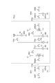
- FIG. 1 is a diagram schematically illustrating a distance measuring device according to an embodiment.
- FIG. 2 is a diagram schematically illustrating an example of a sensor.
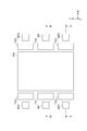
- FIG. 3 is a plan view showing an example of one pixel unit in the sensor.
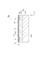
- FIG. 4 is a diagram showing a cross-sectional configuration along the line IV-IV in FIG.
- FIG. 5 is a diagram showing a cross-sectional configuration along the line VV in FIG.
- FIG. 6 is a circuit diagram of one pixel unit of the sensor unit and a corresponding sample hold circuit for the pixel unit.
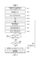
- FIG. 7 is a flowchart showing the control and calculation of the processing unit.
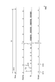
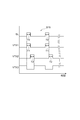
- FIG. 8 is a timing chart of various signals used in the distance measuring apparatus.
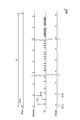
- FIG. 9 is a timing chart of various signals used in the distance measuring device.
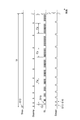
- FIG. 10 is a timing chart of various signals used in the distance measuring device.
- FIG. 11 is a timing chart of various signals used in the distance measuring device.
- FIG. 12 is a timing chart of various signals used in the distance measuring device.
- FIG. 13 is a timing chart of various signals used in the distance measuring device.
- FIG. 14 is a timing chart of various signals used in the distance measuring device.
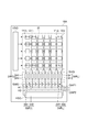
- FIG. 15 is a diagram schematically illustrating an example of a sensor according to another embodiment.
- FIG. 16 is a circuit diagram of one pixel unit of a sensor unit according to another embodiment and a corresponding sample and hold circuit for the pixel unit.
- FIG. 1 is a diagram schematically showing a distance measuring apparatus according to the present embodiment.
- the distance measuring apparatus 10 shown in FIG. 1 calculates
- the distance measuring device 10 includes a light source unit 12, a sensor unit 14, and a processing unit 16.
- the light source unit 12 emits modulated light.
- the light source unit 12 may include a laser diode 12a, a reflecting member 12b, and a driver circuit 12c.
- the driver circuit 12c supplies a modulation current synchronized with the drive pulse signal from the processing unit 16 to the laser diode 12a.
- the laser diode 12a emits modulated light according to the modulation current.
- the modulated light can include, for example, one or more pulsed lights.
- the laser diode 12a emits pulsed light toward the reflecting member 12b.
- the reflecting member 12b reflects the pulsed light emitted from the laser diode 12a.
- the target is irradiated with the pulsed light reflected by the reflecting member 12b.
- the driver circuit 12c sends a drive signal to the actuator of the reflecting member 12b according to the control of the processing unit 16.
- the driver circuit 12c drives the actuator so as to change the optical path of the pulsed light emitted from the laser diode 12a toward the reflecting member 12b.
- the actuator deflects the angle of the reflecting member 12b by a drive signal from the driver circuit 12c.
- the irradiation position of the pulsed light emitted from the laser diode 12a onto the object is scanned by the deflection of the angle of the reflecting member 12b.
- the reflecting member 12b is, for example, a MEMS (Micro Electro Mechanical Systems) mirror.
- the sensor unit 14 includes a sensor 18, a digital-analog conversion unit (DAC) 20, and an analog-digital conversion unit (ADC) 22.
- the digital-analog converter 20 converts the digital signal from the signal processor 16a of the processor 16 into an analog signal.
- the digital-analog converter 20 supplies an analog signal to the sensor 18.
- the analog-digital conversion unit 22 converts an analog signal from the sensor 18 into a digital signal.
- the analog-digital conversion unit 22 supplies the digital signal to the processing unit 16.
- the processing unit 16 calculates the distance by controlling the emission timing of the modulated light of the light source unit 12 and the sensor unit 14.
- the processing unit 16 includes a signal processing unit 16a and a memory 16b.
- the signal processing unit 16a is an arithmetic circuit such as an FPGA (Field-Programmable Gate Array).
- the memory 16b is, for example, an SRAM (Static Random Access Memory).
- FIG. 2 is a diagram schematically showing an example of a sensor.
- the sensor 18 includes an imaging region IR, a sample and hold circuit group SHG, a switch group SWG, a horizontal shift register group HSG, signal lines H1 and H2, and output amplifiers OAP1 and OAP2.
- the sensor 18 is, for example, a line sensor that acquires a line of images.
- the imaging region IR includes a plurality of pixel units P (j) arranged in the horizontal direction.
- j is an integer from 1 to J.
- J is an integer of 2 or more and indicates the number of pixel units.
- FIG. 3 is a plan view showing an example of one pixel unit in the sensor.
- 4 is a diagram showing a cross-sectional configuration along line IV-IV in FIG. 3
- FIG. 5 is a diagram showing a cross-sectional configuration along line VV in FIG.
- Each pixel unit P (1) to P (J) has the configuration shown in FIGS.
- the pixel unit P (j) includes a semiconductor substrate SB.
- the semiconductor substrate SB is, for example, a silicon substrate.
- the semiconductor substrate SB includes a first semiconductor region SR1 and a second semiconductor region SR2.
- the first semiconductor region SR1 is a p-type semiconductor region that provides one main surface SBF1 of the semiconductor substrate SB.
- the second semiconductor region SR2 is a p ⁇ type semiconductor region disposed on the first semiconductor region SR1.
- the impurity concentration of the second semiconductor region SR2 is less than or equal to the impurity concentration of the first semiconductor region SR1.
- the semiconductor substrate SB is formed, for example, by depositing a p ⁇ type semiconductor region by an epitaxial growth method on a p type semiconductor substrate.
- An insulating film ISL is formed on the other main surface SBF2 of the semiconductor substrate SB. Insulating film ISL, for example, constituted by SiO 2.
- a photogate electrode PG is disposed on the insulating film ISL.
- the photogate electrode PG is made of polysilicon, for example. As shown in FIG. 3, in the present embodiment, the photogate electrode PG may have a substantially rectangular planar shape.
- a region located below the photogate electrode PG functions as a light sensitive region that generates charges in response to incident light.
- the first transfer electrode TX1, the second transfer electrode TX2, and the third transfer electrode TX3 are arranged on the insulating film ISL. These transfer electrodes TX1 to TX3 are made of polysilicon, for example. As shown in FIGS. 3 to 5, the first transfer electrode TX1 and the second transfer electrode TX2 are arranged so that the photogate electrode PG exists between them.
- the two third transfer electrodes TX3 have a direction (hereinafter referred to as “Y direction”) that intersects a direction in which the first transfer electrode TX1 and the second transfer electrode TX2 are arranged (hereinafter referred to as “X direction”). ),
- the first transfer electrode TX1 is disposed between the two third transfer electrodes TX3.
- the other two third transfer electrodes TX3 are arranged such that the second transfer electrode TX2 is positioned on the other two third transfer electrodes TX3 in the Y direction.
- a first accumulation region fd1 and a second accumulation region fd2 are formed in the second semiconductor region SR2.
- the first accumulation region fd1 and the second accumulation region fd2 accumulate charges transferred from the photosensitive region.
- the first accumulation region fd1 and the second accumulation region fd2 are arranged so that the photosensitive region is located between the first accumulation region fd1 and the second accumulation region fd2.
- the first accumulation region fd1 and the second accumulation region fd2 are, for example, n + type semiconductor regions doped with n-type impurities at a high concentration.
- the insulating film ISL defines an opening above the first accumulation region fd1 and the second accumulation region fd2.
- An electrode 13 is disposed in these openings.
- the electrode 13 is made of, for example, tungsten provided via a Ti / TiN film.
- the first transfer electrode TX1 is disposed between the electrode 13 on the first accumulation region fd1 and the photogate electrode PG.
- a voltage VTX1 that reduces the potential of the semiconductor region below the first transfer electrode TX1 is applied to the first transfer electrode TX1.
- the voltage VTX1 is given from the digital-analog converter 20 based on the digital signal from the signal processor 16a.
- the second transfer electrode TX2 is disposed between the electrode 13 on the second accumulation region fd2 and the photogate electrode PG.
- a voltage VTX2 that reduces the potential of the semiconductor region below the second transfer electrode TX2 is applied to the second transfer electrode TX2.
- the voltage VTX2 is given from the digital-analog conversion unit 20 based on the digital signal from the signal processing unit 16a.
- an n + type semiconductor region SR3 is formed in the second semiconductor region SR2.
- four semiconductor regions SR3 are arranged.
- the pair of semiconductor regions SR3 is arranged so that the photosensitive region is located between the pair of semiconductor regions SR3.
- Another pair of semiconductor regions SR3 is arranged such that the photosensitive region is located between the other pair of semiconductor regions SR3.
- the insulating film ISL defines an opening above each semiconductor region SR3.
- An electrode 13 is disposed in these openings.
- the electrode 13 is made of, for example, tungsten provided via a Ti / TiN film.
- a corresponding third transfer electrode TX3 is disposed between the electrode 13 on one semiconductor region SR3 and the photogate electrode PG.
- the voltage VTX3 By applying the voltage VTX3 to the third transfer electrode TX3, the potential of the semiconductor region below the third transfer electrode TX3 is reduced.
- the potential of the semiconductor region below the third transfer electrode TX3 charges are transferred from the photosensitive region to the semiconductor region SR3.
- the voltage VTX3 is supplied from the digital-analog conversion unit 20 based on the digital signal from the signal processing unit 16a.
- the electrode 13 in the semiconductor region SR3 is also connected to a predetermined potential Vdd (see FIG. 6).
- This potential Vdd is set by the digital-analog converter 20 based on the digital signal from the signal processor 16a.
- FIG. 6 is a circuit diagram of one pixel unit of the sensor unit and a corresponding sample hold circuit for the pixel unit.
- the sample and hold circuit group SHG of the sensor 18 includes J first sample and hold circuits SH1 and J second sample and hold circuits SH2.
- Each first sample hold circuit SH1 and each second sample hold circuit SH2 are connected to a corresponding pixel unit P (j) (a corresponding pixel unit among the pixel units P (1) to P (J)).
- the sample and hold circuit group SHG includes J sample and hold circuit pairs SHP (1) to SHP (J) each including one first sample and hold circuit SH1 and one second sample and hold circuit.
- J sample-and-hold circuit pairs SHP (1) to SHP (J) are associated with pixel units P (1) to P (J), respectively.
- the pixel unit P (j) includes a first reset switch RS1, a second reset switch RS2, and charge-voltage conversion circuits A1 and A2.
- the first reset switch RS1 is located between the reset potential Vr and the electrode 13 on the first accumulation region fd1.
- the second reset switch RS2 is located between the reset potential Vr and the electrode 13 on the second accumulation region fd2.
- the reset potential Vr is set by the digital-analog converter 20 based on the digital signal from the signal processor 16a.
- the reset pulse signal Sres is given to the first reset switch RS1 and the second reset switch RS2 from the signal processing unit 16a.
- the reset pulse signal Sres is supplied to the first reset switch RS1 and the second reset switch RS2
- the first accumulation region fd1 and the second accumulation region fd2 are connected to the reset potential Vr.
- the charge in the first accumulation region fd1 and the charge in the second accumulation region fd2 are reset.
- the period from the timing when the charges in the first accumulation region fd1 and the second accumulation region fd2 are reset to the next reset timing is a frame period Tf (see FIG. 8).
- the input of the charge-voltage conversion circuit A1 is connected to the electrode 13 on the first accumulation region fd1.
- the output of the charge-voltage conversion circuit A1 is connected to the switch SW10 of the first sample hold circuit SH1.
- the charge-voltage conversion circuit A1 converts the amount of charge in the first accumulation region fd1 into a voltage, and provides the voltage to the first sample hold circuit SH1.
- the input of the charge-voltage conversion circuit A2 is connected to the electrode 13 on the second accumulation region fd2.
- the output of the charge-voltage conversion circuit A2 is connected to the switch SW12 of the second sample and hold circuit SH2.
- the charge-voltage conversion circuit A2 converts the amount of charge in the second accumulation region fd2 into a voltage, and provides the voltage to the second sample hold circuit SH2.
- the first sample and hold circuit SH1 includes a switch SW10 and a capacitor CP10.
- the second sample and hold circuit SH2 includes a switch SW12 and a capacitor CP12.
- the sampling pulse signal Ssamp is given to the switch SW10 and the switch SW12 from the signal processing unit 16a.
- the sampling pulse signal Ssamp is supplied to the switches SW10 and SW12, the output of the charge-voltage conversion circuit A1 and the capacitor CP10 are connected, and the output of the charge-voltage conversion circuit A2 and the capacitor CP12 are connected.
- the output voltage of the charge-voltage conversion circuit A1 is held across the capacitor CP10, and the output voltage of the charge-voltage conversion circuit A2 is held across the capacitor CP12.
- a period from when the sampling pulse signal Ssamp is applied until the next sampling pulse signal Ssamp is applied, that is, between two consecutive sampling pulse signals Ssamp is a reading period.
- the switch group SWG of the sensor 18 includes J switches SW1 and J switches SW2.
- Each switch SW1 and each switch SW2 is a capacitor CP10 of the first sample hold circuit SH1 and a capacitor of the second sample hold circuit SH2 for the corresponding pixel unit among the pixel units P (1) to P (J), respectively.
- the J switch pairs SWP (1) to SWP (J) are associated with the sample and hold circuit pairs SHP (1) to SHP (J), respectively.
- a read pulse signal Sread is applied to the switches SW1 and SW2.
- the read pulse signal Sread is supplied from the horizontal shift register group HSG.
- the horizontal shift register group HSG has J horizontal shift registers.
- the horizontal shift register includes, for example, a flip-flop. These horizontal shift registers are arranged in the arrangement direction of the pixel units P (1) to P (J).
- a start signal is given to the horizontal shift register located at one end in the horizontal shift register group HSG from the signal processing unit 16a. All horizontal shift registers are supplied with a clock signal from the signal processing unit 16a. In response to the start signal and the clock signal, the J horizontal shift registers sequentially apply the read pulse signal Sread to the switch pairs SWP (1) to SWP (J).
- the read pulse signal Sread is applied, so that the first sample hold circuit SH1 and the second sample hold circuit SH2 of the sample hold circuit pair SHP (1) to SHP (J) are connected to the signal line H1 and the signal line. Sequentially connected to H2.
- the capacitor CP10 of the first sample hold circuit SH1 and the capacitor CP12 of the second sample hold circuit SH2 are connected to the signal line H1 and the signal line H2, respectively.
- the voltage held in the first sample hold circuit SH1 is input to the output amplifier OAP1 via the signal line H1.
- the voltage held in the second sample hold circuit SH2 is input to the output amplifier OAP2 via the signal line H2.
- Each of the output amplifier OAP1 and the output amplifier OAP2 amplifies the input voltage and outputs the amplified voltage to the analog-digital conversion unit 22.
- the analog-digital converter 22 converts the input voltage signal into a digital value having a value corresponding to the magnitude of the voltage signal.
- the digital value output by the analog-digital conversion unit 22 is stored in the memory 16b of the processing unit 16.
- a digital value based on the voltage signal from the output amplifier OAP1 is stored in the memory 16b as a first read value to be described later.
- the first read value becomes smaller as the amount of accumulated charge in the first accumulation region fd1 is larger.
- a digital value based on the voltage signal from the output amplifier OAP2 is stored in the memory 16b as a second read value to be described later.
- the second read value becomes smaller as the amount of accumulated charge in the second accumulation region fd2 increases.
- FIG. 7 is a flowchart showing the control and calculation of the processing unit.
- 8 and 9 are timing charts of various signals used in the distance measuring device.
- the processing unit 16 performs control and calculation described below with reference to FIGS. 7 to 9 for each pixel unit.
- the processing unit 16 first has N first read values D1 (0,..., N) and second read values D2 in a non-light emitting frame period in which modulated light is not emitted from the light source unit 12. (0,..., N) is acquired from the sensor unit 14 (S11 in FIG. 7).
- the signal processing unit 16a gives the sampling pulse signal Ssamp to the switch SW10 and the switch SW12 before the start of the first charge transfer cycle.
- a voltage corresponding to the amount of charge accumulated in the first accumulation region fd1 at a time point before the first charge transfer cycle is held in the first sample hold circuit SH1.
- a voltage corresponding to the amount of charge accumulated in the second accumulation region fd2 at the time point before the first charge transfer cycle is held in the second sample hold circuit SH2.
- the signal processing unit 16a sends a start signal and a clock signal to the horizontal shift register group HSG so that the read pulse signal Sread is supplied to the switches SW1 and SW2 from the horizontal shift register. Accordingly, the processing unit 16 acquires the first read value D1 (0) and the second read value D2 (0) from the sensor unit 14.
- the signal processing unit 16a executes the first to Nth charge transfer cycles and the first to Nth read cycles as described below.
- N is a numerical value indicating the order of a predetermined maximum charge transfer cycle.
- the symbol “n” is used as an index indicating the order of the read cycles.
- the signal processing unit 16a provides a digital signal to the sensor unit 14 so that the high-level voltage signal VTX1 is applied to the first transfer electrode TX1 in the first transfer period T1 of the nth charge transfer cycle. Accordingly, in the first transfer period T1, the potential of the semiconductor region below the first transfer electrode TX1, that is, the semiconductor region between the photosensitive region and the first accumulation region fd1, is decreased. Charge is transferred from the region to the first accumulation region fd1.
- the signal processing unit 16a provides a digital signal to the sensor unit 14 so that the high-level voltage signal VTX2 is applied to the second transfer electrode TX2 within the second transfer period T2 of the nth charge transfer cycle. Accordingly, in the second transfer period T2, the potential of the semiconductor region below the second transfer electrode TX2, that is, the semiconductor region between the photosensitive region and the second accumulation region fd2, is decreased. Charge is transferred from the region to the second accumulation region fd2.
- the first transfer period T1 and the second transfer period T2 in the non-light emitting frame period are set similarly to the first transfer period T1 and the second transfer period T2 in the light emitting frame period described later.
- the total length of the first transfer period T1 in each charge transfer cycle in the non-light emitting frame period is the same as the total length of the first transfer period T1 in each charge transfer cycle in the light emitting frame period.
- the total length of the second transfer period T2 in each charge transfer cycle in the non-light emitting frame period is the same as the total length of the second transfer period T2 in each charge transfer cycle in the light emitting frame period.
- the signal processing unit 16a detects the digital signal so that the low-level voltage signal VTX3 is applied to the third transfer electrode TX3. Part 14 is given. Therefore, during the first transfer period T1 and the second transfer period T2, the potential of the semiconductor region between the photosensitive region and the semiconductor region SR3 is maintained high, so that it occurs in the photosensitive region. The charge is not transferred to the semiconductor region SR3.
- the high-level voltage signal VTX3 is supplied to the third transfer electrode TX3 during a period other than the first transfer period T1 and the second transfer period T2. Accordingly, in a period other than the first transfer period T1 and the second transfer period T2, the charge generated in the photosensitive region is transferred to the semiconductor region SR3 and removed.
- the signal processing unit 16a supplies the sampling pulse signal Ssamp to the switch SW10 and the switch SW12 at a time point between the end point of the nth charge transfer cycle and the start point of the (n + 1) th charge transfer cycle.
- a voltage corresponding to the amount of charge accumulated in the first accumulation region fd1 at a time alternated with a plurality of charge transfer cycles is held in the first sample hold circuit SH1, and the second accumulation region at that time.
- a voltage corresponding to the amount of charge accumulated in fd2 is held in the second sample hold circuit SH2.
- the signal processing unit 16a supplies a start signal and a clock signal to the horizontal shift register group HSG so that the read pulse signal Sread is supplied from the horizontal shift register to the switches SW1 and SW2 in the n-th read cycle.
- the processing unit 16 acquires the first read value D1 (n) and the second read value D2 (n) from the sensor unit 14.
- the processing unit 16 acquires the first read value D1 (0,..., N) and the second read value D2 (0,..., N) from the sensor unit 14, and stores these read values in the memory 16b. .
- the processing unit 16 does not cause the light source unit 12 to emit modulated light. Therefore, the first read value D1 (0,..., N) and the second read value D2 (0,..., N) obtained in the non-light emitting frame period reflect only noise components such as background light.
- the first read value D1 (0,..., N) and the second read value D2 (1,..., N) are the first read value Q1 (0,. N) and second read values Q201,..., N) are subtracted to remove noise components such as background light.
- the signal processing unit 16a of the processing unit 16 applies a reset pulse signal Sres to the first reset switch RS1 and the second RS2, and sets the first storage region fd1 and the second storage region fd2 to the reset potential Vr. Connect to.
- the charge accumulated in the first accumulation region fd1 and the charge accumulated in the second accumulation region fd2 are reset (S12 in FIG. 7), and the light emission frame period which is the next frame period Tf is started.
- a drive pulse signal is given to the light source unit 12 from the signal processing unit 16a, and the light source unit 12 emits modulated light at a predetermined timing.
- the processing unit 16 acquires the first read value Q1 (0) and the second read value Q2 (0) from the sensor unit 14, and the first read value Q1 (0) and The second read value Q2 (0) is stored in the memory 16b as the first read value and the initial value of the second read value (S13 in FIG. 7).
- the signal processing unit 16a gives the sampling pulse signal Ssamp to the switch SW10 and the switch SW12 before the start of the first charge transfer cycle Cy.
- a voltage corresponding to the amount of charge accumulated in the first accumulation region fd1 at a time point before the first charge transfer cycle is held in the first sample hold circuit SH1, and at the time point, the second accumulation region A voltage corresponding to the amount of charge accumulated in fd2 is held in the second sample hold circuit SH2.
- the signal processing unit 16a sends a start signal and a clock signal to the horizontal shift register group HSG so that the read pulse signal Sread is supplied to the switches SW1 and SW2 from the horizontal shift register. Accordingly, the processing unit 16 acquires the first read value Q1 (0) and the second read value Q2 (0) from the sensor unit 14. That is, the charge accumulated in the nth charge transfer cycle Cy is read in a read cycle between the end time of the nth charge transfer cycle Cy and the start time of the n + 1th charge transfer cycle Cy.
- the first read value Q1 (0) and the second read value Q2 (0) are output from the first accumulation region fd1 at the time when the first sampling pulse signal Ssamp is output, that is, at the time before the first charge transfer cycle. Respectively corresponding to the amount of charge accumulated in the second accumulation region fd2. Therefore, the first read value Q1 (0) and the second read value Q2 (0) do not reflect the signal light component generated when the modulated light from the light source unit 12 is reflected from the object.
- a read period (a period between two consecutive sampling pulse signals Ssamp) includes a charge transfer cycle Cy and a read cycle.
- the signal processing unit 16 a gives one or more driving pulse signals SL to the light source unit 12 in the n-th charge transfer cycle Cy, and sends modulated light from the light source unit 12 to the driving pulse signal. Release the same number of times as SL (S15 in FIG. 7). In other words, in the n-th charge transfer cycle Cy, the number m of emission periods of the modulated light from the light source unit 12 is one or more. The time length of each release period is T0, as also shown in FIG.
- the signal processing unit 16a also applies a digital signal so that the high-level voltage signal VTX1 is applied to the first transfer electrode TX1 within the first transfer period T1 of the nth charge transfer cycle Cy. Is provided to the sensor unit 14.
- the signal processing unit 16a provides a digital signal to the sensor unit 14 so that the high-level voltage signal VTX2 is applied to the second transfer electrode TX2 within the second transfer period T2 of the nth charge transfer cycle Cy.
- the first transfer period T1 is synchronized with the drive pulse signal SL. That is, the rising timing of the drive pulse signal SL and the rising timing of the voltage signal VTX1 are substantially synchronized.
- the duration T0 of the drive pulse signal SL and the first transfer period T1 have substantially the same length of time.
- the second transfer period T2 is phase-inverted with the first transfer period T1. That is, in each charge transfer cycle Cy, the phase of the second transfer period T2 is delayed by 180 degrees from the phase of the first transfer period T1. More specifically, the falling timing of the voltage signal VTX1 and the rising timing of the voltage signal VTX2 are substantially synchronized.
- the first transfer period T1 and the second transfer period T2 have substantially the same time length.
- the signal processing unit 16a detects the digital signal so that the low-level voltage signal VTX3 is applied to the third transfer electrode TX3. Part 14 is given.
- the third transfer electrode TX3 is supplied with a high-level voltage signal VTX3 during a period other than the first transfer period T1 and the second transfer period T2. Therefore, in the first transfer period T1 and the second transfer period T2, the charge corresponding to the incident light to the photosensitive region is not transferred to the semiconductor region SR3. However, in a period other than the first transfer period T1 and the second transfer period T2, the charge generated in the photosensitive region is transferred to the semiconductor region SR3 and removed.
- the first transfer period T1 is provided in synchronization with the modulated light emission period of each time, and the second transfer period T2 that is phase-inverted with the first transfer period T1 is provided. Accordingly, in the nth charge transfer cycle Cy, the same number of first transfer periods T1 as the number of drive pulse signals SL and the same number of second transfer periods T2 as the number of drive pulse signals SL are provided. ing. In the n-th charge transfer cycle Cy, the length of time for which charges are accumulated in the first accumulation region fd1 is the product of the first transfer period T1 (time T0) and the number of times of the drive pulse signal SL (number of times of emission). It is.
- the length of time for which charges are accumulated in the second accumulation region fd2 is the product of the second transfer period T2 (time T0) and the number of times of the drive pulse signal SL (number of times of emission). It is.
- the signal processing unit 16a obtains the first read value Q1 (n) and the second read value Q2 (n) from the sensor unit 14, and the first read value Q1 (n) and the second read value Q2 (n)
- the read value Q2 (n) is stored in the memory 16b (S16 in FIG. 7).
- the signal processing unit 16a supplies the sampling pulse signal Ssamp to the switch SW10 and the switch SW12 between the end point of the nth charge transfer cycle Cy and the start point of the (n + 1) th charge transfer cycle Cy.
- the voltage corresponding to the amount of charge accumulated in the first accumulation region fd1 at the time alternate with the plurality of charge transfer cycles Cy is held in the first sample hold circuit SH1, and the second accumulation at that time.
- a voltage corresponding to the amount of charge accumulated in the region fd2 is held in the second sample hold circuit SH2.
- the signal processing unit 16a supplies a start signal and a clock signal to the horizontal shift register group HSG so that the read pulse signal Sread is supplied from the horizontal shift register to the switches SW1 and SW2 in the n-th read cycle.
- the processing unit 16 acquires the first read value Q1 (n) and the second read value Q2 (n) from the sensor unit 14. That is, the charge accumulated in the nth charge transfer cycle Cy is read in a read cycle between the end time of the nth charge transfer cycle Cy and the start time of the n + 1th charge transfer cycle Cy.
- the first read value Q1 (n) is stored in the first storage region fd1 at the time between the end of the nth charge transfer cycle Cy and the start of the (n + 1) th charge transfer cycle Cy.
- the second read value Q2 (n) is a value corresponding to the amount of charge stored in the second storage region fd2 at that time.
- the signal processing unit 16a obtains the first difference value k1 (n) and the second difference value k2 (n) (S17 in FIG. 7).
- the first difference value k1 (n) is obtained by subtracting the first read value Q1 (n-1) of the (n-1) th read cycle from the first read value Q1 (n) of the nth read cycle. Is required.
- the second difference value k2 (n) is obtained by subtracting the second read value Q2 (n-1) of the (n-1) th read cycle from the second read value Q2 (n) of the nth read cycle. It is calculated by.
- the signal processing unit 16a obtains the predicted value Q1 (n + 1) and the predicted value Q2 (n + 1) (S18 in FIG. 7).
- the predicted value Q1 (n + 1) is obtained by adding the first difference value k1 (n) to the first read value Q1 (n) of the nth read cycle.
- the predicted value Q2 (n + 1) is obtained by adding the second difference value k2 (n) to the second read value Q2 (n) of the nth read cycle.
- the predicted value Q1 (n + 1) is the predicted value of the first read value of the (n + 1) th read cycle
- the predicted value Q2 (n + 1) is the predicted value of the second read value of the (n + 1) th read cycle.
- the signal processing unit 16a compares the first predicted value Q1 (n + 1) and the second predicted value Q2 (n + 1) with a predetermined threshold value Qth (S19 in FIG. 7).
- the threshold value Qth is equal to or higher than the first read value corresponding to the saturated storage capacity of the first storage region fd1, and the second threshold value corresponding to the saturation storage capacity of the second storage region fd2 is set. The value is set to be greater than or equal to the read value.
- the determination result of the process in S19 is “No”.
- the process of the signal processing unit 16a proceeds to the process of S20.
- the signal processing unit 16a increments the value of n by 1 (S21 in FIG. 7), and repeats the processing from S15.
- the process of the signal processing unit 16a proceeds to S22.
- the processing unit 16a stops the (n + 1) th read cycle. That is, the signal processing unit 16a acquires the first read value and the second read value from the sensor unit 14 in the (n + 1) th and subsequent read cycles, and the first read value and the second read value in the (n + 1) th and subsequent read cycles. Storage of the read value in the memory 16b is stopped.
- the threshold value Qth is equal to the larger read value of the first read value corresponding to the saturated storage capacity of the first storage region fd1 and the second read value corresponding to the saturated storage capacity of the second storage region fd2.
- the processing unit 16 can acquire the first read value Q1 (n) in a range not exceeding the read value corresponding to the saturated storage capacity of the first storage region fd1, and the processing unit 16 Can acquire the second read value Q2 (n) in a range not exceeding the read value corresponding to the saturated storage capacity of the second storage region fd2.
- the dynamic range of the measurement distance can be improved.
- the distance measurement accuracy is improved. Furthermore, it is possible to start calculation after the processing in S22 of the signal processing unit 16a at an early stage.
- the threshold value Qth is larger of the first read value corresponding to the saturated storage capacity of the first storage region fd1 and the second read value corresponding to the saturated storage capacity of the second storage region fd2. It may be set to a value larger than the other read value.
- the sensor unit 14 can be used in a range in which the linearity of the relationship between the accumulated charge amount and the incident light amount of each of the first accumulation region fd1 and the second accumulation region fd2 is excellent. Therefore, the distance measurement accuracy is further improved.
- the signal processing unit 16a creates an approximate expression based on the second read values Q2 (0) to Q2 (n) up to the nth read cycle which is the final read cycle, and uses the approximate expression.
- a correction value Q2corr for the second read value Q2 is calculated.
- the correction value Q1corr of the first read value Q1 is the correction value of the first read value Q1 (n) in the nth read cycle
- the correction value Q2corr of the second read value Q2 is , The correction value of the second read value Q2 (n) of the nth cycle.
- the correction values Q1corr and Q2Corr are correction values obtained as an output of an approximate expression, the number of the corresponding read cycle is not limited.
- the approximate expression is created based on, for example, the least square method. As the approximate expression, other known approximate expression creation methods may be used.
- the signal processing unit 16a calculates a correction value for the read value D1 using an approximate expression based on the read values D1 (0) to D1 (n), and uses the correction value for the read value D1 as the first read value Q1.
- the first estimated value Q1est may be calculated by subtracting from the sum of the correction value Q1corr and the first read value Q1 (0).
- the correction value of the read value D1 and the correction value Q1corr of the read value Q1 are the correction value of the read value D1 and the correction value of the read value Q1 of the read cycle in the same order.
- the signal processing unit 16a calculates a correction value for the read value D2 using an approximate expression based on the read values D2 (0) to D2 (n), and uses the correction value for the read value D2 as the second read value.
- the second estimated value Q2est may be calculated by subtracting from the sum of the correction value Q2corr of Q2 and the second read value Q2 (0).
- the correction value of the read value D2 and the correction value Q2corr of the read value Q2 are the correction value of the read value D2 and the correction value of the read value Q2 in the same read cycle.
- the first estimated value Q1est is a noise component such as background light obtained in another frame period from the sum of the correction value of the first read value calculated using the approximate expression and the first read value Q1 (0). Is a value obtained by subtracting the first read value corresponding to.
- the second estimated value Q2est is a noise component such as background light obtained in another frame period from the sum of the correction value of the second read value calculated using the approximate expression and the first read value Q1 (0). Is a value obtained by subtracting the second read value corresponding to. Therefore, even if a part of the first read value and the second read value acquired by the final read cycle fluctuates due to a disturbance or the like, the first estimated value Q1est and the second estimated value based on the approximate expression are used. In Q2est, the influence of the read value including fluctuation is reduced. In the first estimated value Q1est and the second estimated value Q2est, the influence of noise such as background light is reduced.
- the signal processing unit 16a calculates a distance (S23 in FIG. 7). Specifically, the signal processing unit 16a calculates the distance L by the calculation of the following formula (3).
- L (1/2) ⁇ c ⁇ T0 ⁇ ⁇ Q2est ⁇ ⁇ / (Q1est + Q2est ⁇ ⁇ ) ⁇ c is the speed of light.
- ⁇ is a ratio between the first read value and the second read value when the same amount of incident light is incident on the photosensitive region in the first transfer period T1 and the second transfer period T2.
- the signal processing unit 16a uses the ratio between the first estimated value Q1est based on the accumulated charge amount in the first accumulation region fd1 and the second estimated value Q2est based on the accumulated charge amount in the second accumulation region fd2.
- the distance to the object is calculated with high accuracy.
- the signal processing unit 16a outputs a one-line distance image having a gray value corresponding to the distance calculated for each pixel.
- the signal processing unit 16a may repeat the control and calculation described with reference to FIGS. 7 to 9 so as to update the distance image every frame period Tf.
- the signal processing unit 16a increases the number m of the discharge period per charge transfer cycle Cy within one frame period Tf. Specifically, the signal processing unit 16a increases the number m of emission periods per charge transfer cycle Cy by shortening the period of the emission period. That is, the signal processing unit 16a increases the number m of emission periods per charge transfer cycle Cy by shortening the period of the emission period. The signal processing unit 16a reduces the number m of discharge periods per charge transfer cycle Cy by increasing the period of the discharge period.
- the period of the discharge period at the beginning of one frame period Tf is longer than the period of the discharge period at the latter stage of one frame period Tf. That is, the period of the emission period in the latter stage of one frame period Tf is shorter than the period of the emission period in the initial stage of one frame period Tf.
- the period of the discharge period monotonously decreases within one frame period Tf. In this specification, “monotonically decreasing” means that there is no tendency to increase, and means monotonic decrease in a broad sense.
- the length of the read period is constant, and the period of the charge transfer cycle Cy is not changed.
- the signal processing unit 16a gradually increases the number m of the discharge period per charge transfer cycle Cy. For example, in the initial stage of one frame period Tf, the number m of discharge periods per charge transfer cycle Cy is “2”, and in the latter period of one frame period Tf, discharge per charge transfer cycle Cy is performed.
- the number of periods is “M”. That is, the signal processing unit 16a increases the number of discharge periods per charge transfer cycle Cy in two stages.
- M is a numerical value determined in advance as the maximum value of the number of discharge periods per charge transfer cycle Cy.
- the number m of the discharge period per charge transfer cycle Cy increases monotonously within one frame period Tf.
- “monotonically increasing” means not decreasing, and means monotonically increasing in a broad sense.
- the period of the discharge period is longer than that of the latter period of one frame period Tf.
- the number m is small. For this reason, even when the intensity of the reflected light incident on the pixel unit P (j) of the sensor 18 is strong (for example, when the object is located at a short distance or when the reflectance of the object is high), In the initial stage of one frame period Tf, it is difficult to cause saturation of accumulated signal charges. Therefore, the distance measurement device 10 performs appropriate distance measurement.
- the distance measurement device 10 performs appropriate distance measurement.
- the dynamic range of the intensity of the reflected light can be expanded without changing one frame period Tf.
- the signal processing unit 16a may increase the number m of the discharge period per charge transfer cycle Cy in three or more stages. Further, as shown in FIG. 11, the signal processing unit 16 a may gradually increase the number m of the discharge period per charge transfer cycle Cy from “1” to “M”. In any case, the number m of the discharge period per charge transfer cycle Cy is monotonously increased within one frame period Tf.
- the signal processing unit 16a increases the length of the readout period and lengthens the period of the charge transfer cycle Cy, thereby reducing the number m of discharge periods per charge transfer cycle Cy. It may be increased. That is, the signal processing unit 16a reduces the number m of the discharge period per charge transfer cycle Cy by shortening the length of the read period and the period of the charge transfer cycle Cy, thereby reducing the charge transfer cycle Cy. By extending the period of Cy, the number m of the discharge period per charge transfer cycle Cy is increased.
- the period of the charge transfer cycle Cy at the beginning of one frame period Tf is shorter than the period of the charge transfer cycle Cy at the latter stage of one frame period Tf. That is, the period of the charge transfer cycle Cy at the latter stage of one frame period Tf is longer than the period of the charge transfer cycle Cy at the beginning of one frame period Tf.
- the period of the charge transfer cycle Cy monotonously increases within one frame period Tf.
- the period of the emission period does not change within one frame period Tf.
- the signal processor 16a lengthens the period of the charge transfer cycle Cy in two stages. For example, the number m of discharge periods per charge transfer cycle Cy is “3”, and in the latter period of one frame period Tf, the number of discharge periods per charge transfer cycle Cy is “M”. is there. The number m of the discharge period per charge transfer cycle Cy increases monotonously within one frame period Tf.
- the charge transfer cycle Cy is discharged at the beginning of one frame period Tf because the period of the charge transfer cycle Cy is shorter than the latter period of one frame period Tf.
- the number of periods is small. For this reason, even when the intensity of the reflected light incident on the pixel unit P (j) of the sensor 18 is strong (for example, when the object is located at a short distance or when the reflectance of the object is high), In the initial stage of one frame period Tf, it is difficult to cause saturation of accumulated signal charges. Therefore, the distance measurement device 10 performs appropriate distance measurement.
- the distance measurement device 10 performs appropriate distance measurement.
- the signal processing unit 16a may lengthen the period of the charge transfer cycle Cy by three or more stages. In this case, the number m of the discharge period per charge transfer cycle Cy increases in three or more stages. Further, as shown in FIG. 14, the signal processing unit 16a may gradually increase the period of the charge transfer cycle Cy. In this case, for example, the number m of discharge periods per charge transfer cycle Cy is gradually increased from “1” to “M”. In any case, the number m of the discharge period per charge transfer cycle Cy is monotonously increased within one frame period Tf.
- FIG. 15 is a diagram illustrating an example of a sensor according to another embodiment.
- FIG. 16 is a circuit diagram of one pixel unit of a sensor unit according to another embodiment and a corresponding sample and hold circuit for the pixel unit.
- the distance measuring device 10 may have a sensor 18A shown in FIG.
- the sensor 18A has an imaging region IR having I ⁇ J pixel units P (i, j).
- I is an integer of 1 to I
- j is an integer of 1 to J
- I and J are integers of 2 or more.
- I ⁇ J pixel units P (i, j) are arranged in I rows and J columns.
- two vertical signal lines V1 (j) and V2 (j) for each column of the pixel unit are provided.
- a switch SW20 is connected to the output of the charge-voltage conversion circuit A1 of the pixel unit P (i, j) of the sensor 18A.
- the switch SW20 is connected to the switch SW10 of the corresponding first sample hold circuit SH1 via the corresponding vertical signal line V1 (j).
- a switch SW22 is connected to the output of the charge-voltage conversion circuit A2 of the pixel unit P (i, j).
- the switch SW22 is connected to the switch SW12 of the corresponding second sample and hold circuit SH2 via the corresponding vertical signal line V2 (j).
- the sensor 18A further includes a vertical shift register group VSG.
- the vertical shift register group VSG includes a plurality of vertical shift registers arranged in the vertical direction. Each vertical shift register includes, for example, a flip-flop.
- a start signal is given to the vertical shift register provided at one end in the arrangement direction from the signal processing unit 16a. All the vertical shift registers receive a clock signal from the signal processing unit 16a.
- the vertical shift register group VSG sequentially applies row selection signals to the switches SW20 and SW22 of the plurality of pixel units P (i, j) in the row order.
- the outputs of the charge-voltage conversion circuits A1 and A2 of the plurality of pixel units (i, j) in each column are sequentially connected to the corresponding vertical signal lines V1 (j) and V2 (j), and a plurality of The output voltage of the pixel unit P (i, j) is sequentially held in the row order in the corresponding sample and hold circuits SH1 and SH2.
- the output voltages of the plurality of pixel units (j, i) in each row are held in the corresponding sample hold circuits SH1 and SH2
- the voltages held in the sample hold circuits SH1 and SH2 are given from the horizontal shift register group HSG.
- the read pulse signals are sequentially coupled to the signal lines H1 and H2 in the column order.
- the signal processing part 16a can form a two-dimensional distance image by performing the calculation demonstrated in FIG. 7 about each pixel unit.
- corresponding sample hold circuits SH1 and SH2 are provided for each column of pixel units, but corresponding sample hold circuits SH1 and SH2 are provided for each pixel unit. Also good.
- the number of pixel units in the imaging region IR may be one.
- the number m of the discharge period per charge transfer cycle Cy is not limited to the values shown in FIG. 8 and FIGS.
- Each pixel unit P (1) to P (J) has two photosensitive regions (first ones) as described in Japanese Patent Application Laid-Open Nos. 2013-178121 and 2013-206903 by the applicant of the present application.
- the first accumulation region accumulates charges generated in the first photosensitive region
- the second accumulation region accumulates charges generated in the second photosensitive region.
- the first transfer electrode is provided between the first photosensitive region and the first accumulation region.
- the second transfer electrode is provided between the second photosensitive region and the second accumulation region.
- each of the pixel units P (1) to P (J) are described in the above-described Japanese Patent Application Laid-Open Nos. 2013-178121 and 2013-206903, for example.
- each may be “1”.
- the voltage signal applied to the transfer electrode is intermittently phase-shifted at a predetermined timing.
- the voltage signal is given a phase shift of 180 degrees at a timing of 180 degrees.
- the voltage signal applied to the transfer electrode is synchronized with the drive pulse signal SL at a timing of 0 degrees, and has a phase difference of 180 degrees with respect to the drive pulse signal SL at a timing of 180 degrees. That is, the charge accumulated in the accumulation region is read out at the timing of 0 degrees and the timing of 180 degrees.
- the present invention can be used for a distance measuring device based on the TOF method.
- DESCRIPTION OF SYMBOLS 10 ... Distance measuring device, 12 ... Light source part, 14 ... Sensor part, 16 ... Processing part, 16a ... Signal processing part, 18 ... Sensor, Cy ... Charge transfer cycle, fd1 ... 1st accumulation
Landscapes
- Engineering & Computer Science (AREA)
- Physics & Mathematics (AREA)
- General Physics & Mathematics (AREA)
- Radar, Positioning & Navigation (AREA)
- Remote Sensing (AREA)
- Computer Networks & Wireless Communication (AREA)
- Electromagnetism (AREA)
- Optical Radar Systems And Details Thereof (AREA)
- Measurement Of Optical Distance (AREA)
Abstract
Description
センサ部は、入射光に応じて電荷を発生する光感応領域、光感応領域で発生した電荷を蓄積する蓄積領域、光感応領域と蓄積領域との間に設けられた転送電極、及び、蓄積領域とリセット電位との間に設けられたリセットスイッチを有している。処理部は、変調光の放出タイミング及びセンサ部を制御して、距離を算出する。処理部は、リセットスイッチを制御して蓄積領域をリセット電位に接続してから該蓄積領域を次にリセット電位に接続するまでのフレーム期間内の複数の電荷転送サイクルにおいて、一以上の放出期間に光源部に変調光を放出させ、かつ、電荷転送サイクル一回あたりの放出期間の数を一つのフレーム期間内で増加させる。処理部は、一以上の放出期間に同期した一以上の転送期間に転送電極に与える電圧を制御して光感応領域で発生した電荷を蓄積領域に蓄積させる。処理部は、複数の電荷転送サイクルのそれぞれに対応する複数の読出しサイクルにおいて、複数の電荷転送サイクルと交互の時点に蓄積領域に蓄積されている電荷量に応じた複数の読出し値をセンサ部から取得する。処理部は、複数の読出し値に基づいて、距離を算出する。
<式(1)>
Q1est=Q1corr+Q1(0)-D1(n)
<式(2)>
Q2est=Q2corr+Q2(0)-D2(n)
<式(3)>
L=(1/2)×c×T0×{Q2est×α/(Q1est+Q2est×α)}
cは、光速である。αは、同量の入射光が第1の転送期間T1及び第2の転送期間T2に光感応領域に入射したときの第1の読出し値と第2の読出し値の比である。このように、信号処理部16aは、第1の蓄積領域fd1の蓄積電荷量に基づく第1の推定値Q1estと第2の蓄積領域fd2の蓄積電荷量に基づく第2の推定値Q2estの比により、対象物に対する距離を高精度に算出する。本実施形態においては、信号処理部16aは、各画素について算出した距離に応じた濃淡値を有する1行の距離画像を出力する。本実施形態においては、信号処理部16aはフレーム期間Tfごとに距離画像を更新するよう、図7~図9を用いて説明した制御及び演算を繰り返してもよい。
Claims (8)
- 飛行時間法により対象物に対する距離を求める距離測定装置であって、
変調光を放出する光源部と、
入射光に応じて電荷を発生する光感応領域、前記光感応領域で発生した電荷を蓄積する蓄積領域、前記光感応領域と前記蓄積領域との間に設けられた転送電極、及び、前記蓄積領域とリセット電位との間に設けられたリセットスイッチを有するセンサ部と、
前記変調光の放出タイミング及び前記センサ部を制御して、距離を算出する処理部と、を備え、
前記処理部は、
前記リセットスイッチを制御して前記蓄積領域を前記リセット電位に接続してから当該蓄積領域を次に前記リセット電位に接続するまでのフレーム期間内の複数の電荷転送サイクルにおいて、一以上の放出期間に前記光源部に前記変調光を放出させ、かつ、前記電荷転送サイクル一回あたりの前記放出期間の数を一つの前記フレーム期間内で増加させ、
前記一以上の放出期間に同期した一以上の転送期間に前記転送電極に与える電圧を制御して前記光感応領域で発生した電荷を前記蓄積領域に蓄積させ、
前記複数の電荷転送サイクルのそれぞれに対応する複数の読出しサイクルにおいて、前記複数の電荷転送サイクルと交互の時点に前記蓄積領域に蓄積されている電荷量に応じた複数の読出し値を前記センサ部から取得し、
前記複数の読出し値に基づいて、距離を算出する。 - 請求項1に記載の距離測定装置であって、
前記処理部は、放出期間の周期を短くすることにより、前記電荷転送サイクル一回あたりの前記放出期間の数を増加させる。 - 請求項1に記載の距離測定装置であって、
前記処理部は、電荷転送サイクルの期間を長くすることにより、前記電荷転送サイクル一回あたりの前記放出期間の数を増加させる。 - 請求項1~3のいずれか一項に記載の距離測定装置であって、
前記処理部は、前記電荷転送サイクル一回あたりの前記放出期間の数を段階的に増加させる。 - 請求項1~3のいずれか一項に記載の距離測定装置であって、
前記処理部は、前記電荷転送サイクル一回あたりの前記放出期間の数を徐々に増加させる。 - 請求項1~5のいずれか一項に記載の距離測定装置であって、
前記センサ部は、
前記蓄積領域として、第1の蓄積領域及び第2の蓄積領域を含み、
前記転送電極として、前記光感応領域と前記第1の蓄積領域との間に設けられた第1の転送電極、及び、前記光感応領域と前記第2の蓄積領域との間に設けられた第2の転送電極を含み、
前記リセットスイッチとして、前記第1の蓄積領域とリセット電位との間に設けられた第1のリセットスイッチ、及び、前記第2の蓄積領域とリセット電位との間に設けられた第2のリセットスイッチを含み、
前記処理部は、
前記第1のリセットスイッチ及び前記第2のリセットスイッチを制御して前記第1の蓄積領域及び前記第2の蓄積領域を前記リセット電位に接続してから当該第1の蓄積領域及び当該第2の蓄積領域を次に前記リセット電位に接続するまでのフレーム期間内の複数の電荷転送サイクルにおいて、前記一以上の放出期間に同期した一以上の第1の転送期間に前記第1の転送電極に与える電圧を制御して前記光感応領域で発生した電荷を前記第1の蓄積領域に蓄積させ、前記一以上の第1の転送期間と位相反転した一以上の第2の転送期間に前記第2の転送電極に与える電圧を制御して前記光感応領域で発生した電荷を前記第2の蓄積領域に蓄積させ、
前記複数の電荷転送サイクルのそれぞれに対応する複数の読出しサイクルにおいて、前記複数の電荷転送サイクルと交互の時点に前記第1の蓄積領域に蓄積されている電荷量に応じた複数の第1の読出し値及び当該時点に前記第2の蓄積領域に蓄積されている電荷量に応じた複数の第2の読出し値を、前記センサ部から取得し、
前記複数の第1の読出し値及び前記複数の第2の読出し値に基づいて、距離を算出する。 - 請求項6に記載の距離測定装置であって、
前記処理部は、n回目の前記読出しサイクルの前記第1の読出し値と、n回目の前記読出しサイクルの前記第1の読出し値とn-1回目の前記読出しサイクルの前記第1の読出し値との間の差分値との和、又は、n回目の前記読出しサイクルの前記第2の読出し値と、n回目の前記読出しサイクルの前記第2の読出し値とn-1回目の前記読出しサイクルの前記第2の読出し値との間の差分値との和が、所定の閾値を超える場合に、n+1回目以降の前記読出しサイクルを停止し、
ここでnは前記複数の読出しサイクルの順番を示す。 - 請求項6又は7に記載の距離測定装置であって、
前記処理部は、
前記複数の第1の読出し値に基づく近似式を用いて第1の推定値を算出し、前記複数の第2の読出し値に基づく近似式を用いて第2の推定値を算出し、
前記第1の推定値及び前記第2の推定値に基づいて、距離を算出する。
Priority Applications (5)
| Application Number | Priority Date | Filing Date | Title |
|---|---|---|---|
| KR1020177033724A KR102481693B1 (ko) | 2015-04-28 | 2016-04-08 | 거리 측정 장치 |
| CH01201/17A CH712465B1 (de) | 2015-04-28 | 2016-04-08 | Distanzmessvorrichtung. |
| CN201680024207.XA CN107533128B (zh) | 2015-04-28 | 2016-04-08 | 距离测定装置 |
| DE112016001944.0T DE112016001944T5 (de) | 2015-04-28 | 2016-04-08 | Distanzmessvorrichtung |
| US15/567,645 US10871568B2 (en) | 2015-04-28 | 2016-04-08 | Distance measurement device |
Applications Claiming Priority (2)
| Application Number | Priority Date | Filing Date | Title |
|---|---|---|---|
| JP2015091372A JP6554310B2 (ja) | 2015-04-28 | 2015-04-28 | 距離測定装置 |
| JP2015-091372 | 2015-04-28 |
Publications (1)
| Publication Number | Publication Date |
|---|---|
| WO2016175012A1 true WO2016175012A1 (ja) | 2016-11-03 |
Family
ID=57199791
Family Applications (1)
| Application Number | Title | Priority Date | Filing Date |
|---|---|---|---|
| PCT/JP2016/061535 Ceased WO2016175012A1 (ja) | 2015-04-28 | 2016-04-08 | 距離測定装置 |
Country Status (7)
| Country | Link |
|---|---|
| US (1) | US10871568B2 (ja) |
| JP (1) | JP6554310B2 (ja) |
| KR (1) | KR102481693B1 (ja) |
| CN (1) | CN107533128B (ja) |
| CH (1) | CH712465B1 (ja) |
| DE (1) | DE112016001944T5 (ja) |
| WO (1) | WO2016175012A1 (ja) |
Cited By (1)
| Publication number | Priority date | Publication date | Assignee | Title |
|---|---|---|---|---|
| JP2018080997A (ja) * | 2016-11-16 | 2018-05-24 | 株式会社リコー | 距離測定装置及び距離測定方法 |
Families Citing this family (23)
| Publication number | Priority date | Publication date | Assignee | Title |
|---|---|---|---|---|
| USRE46672E1 (en) | 2006-07-13 | 2018-01-16 | Velodyne Lidar, Inc. | High definition LiDAR system |
| US10627490B2 (en) | 2016-01-31 | 2020-04-21 | Velodyne Lidar, Inc. | Multiple pulse, LIDAR based 3-D imaging |
| CN109154661A (zh) | 2016-03-19 | 2019-01-04 | 威力登激光雷达有限公司 | 用于基于lidar的3-d成像的集成照射和检测 |
| US10393877B2 (en) | 2016-06-01 | 2019-08-27 | Velodyne Lidar, Inc. | Multiple pixel scanning LIDAR |
| WO2018183843A1 (en) | 2017-03-31 | 2018-10-04 | Velodyne Lidar, Inc. | Integrated lidar illumination power control |
| EP3392674A1 (en) * | 2017-04-23 | 2018-10-24 | Xenomatix NV | A pixel structure |
| JP2018185179A (ja) * | 2017-04-25 | 2018-11-22 | 株式会社リコー | 測距装置、監視装置、3次元計測装置、移動体、ロボット及び測距方法 |
| CN110809704B (zh) * | 2017-05-08 | 2022-11-01 | 威力登激光雷达美国有限公司 | Lidar数据获取与控制 |
| US11294041B2 (en) | 2017-12-08 | 2022-04-05 | Velodyne Lidar Usa, Inc. | Systems and methods for improving detection of a return signal in a light ranging and detection system |
| US11971507B2 (en) | 2018-08-24 | 2024-04-30 | Velodyne Lidar Usa, Inc. | Systems and methods for mitigating optical crosstalk in a light ranging and detection system |
| US10712434B2 (en) | 2018-09-18 | 2020-07-14 | Velodyne Lidar, Inc. | Multi-channel LIDAR illumination driver |
| US11082010B2 (en) | 2018-11-06 | 2021-08-03 | Velodyne Lidar Usa, Inc. | Systems and methods for TIA base current detection and compensation |
| US12061263B2 (en) | 2019-01-07 | 2024-08-13 | Velodyne Lidar Usa, Inc. | Systems and methods for a configurable sensor system |
| US11885958B2 (en) | 2019-01-07 | 2024-01-30 | Velodyne Lidar Usa, Inc. | Systems and methods for a dual axis resonant scanning mirror |
| CN113287037B (zh) * | 2019-01-15 | 2024-05-07 | 国立大学法人静冈大学 | 距离图像测定装置、距离图像测定系统以及距离图像测定方法 |
| WO2020178920A1 (ja) * | 2019-03-01 | 2020-09-10 | 株式会社ブルックマンテクノロジ | 距離画像撮像装置および距離画像撮像装置による距離画像撮像方法 |
| JP7535793B2 (ja) | 2019-06-25 | 2024-08-19 | 国立大学法人静岡大学 | 距離画像測定装置 |
| US10613203B1 (en) | 2019-07-01 | 2020-04-07 | Velodyne Lidar, Inc. | Interference mitigation for light detection and ranging |
| CN114342355B (zh) * | 2019-09-06 | 2024-03-08 | 松下知识产权经营株式会社 | 摄像装置 |
| DE112020006361T5 (de) * | 2019-12-26 | 2022-10-27 | Hamamatsu Photonics K.K. | Lichtdetektionsvorrichtung und Verfahren zum Betreiben von Photosensor |
| JP6953595B1 (ja) * | 2020-09-09 | 2021-10-27 | 浜松ホトニクス株式会社 | 距離画像取得装置及び距離画像取得方法 |
| CN114335033B (zh) * | 2020-09-30 | 2025-07-11 | 思特威(上海)电子科技股份有限公司 | 测距像素结构及tof图像传感器 |
| JP7833180B2 (ja) * | 2022-06-01 | 2026-03-19 | 株式会社ジャパンディスプレイ | 検出装置 |
Citations (5)
| Publication number | Priority date | Publication date | Assignee | Title |
|---|---|---|---|---|
| JPH10197635A (ja) * | 1997-01-13 | 1998-07-31 | Omron Corp | レーザー測距装置 |
| JP2000275340A (ja) * | 1999-03-25 | 2000-10-06 | Mitsubishi Electric Corp | レーザレーダ装置 |
| WO2009105857A1 (en) * | 2008-02-29 | 2009-09-03 | Institut National D'optique | Light-integrating rangefinding device and method |
| JP2009257780A (ja) * | 2008-04-11 | 2009-11-05 | Mitsubishi Heavy Ind Ltd | 撮像システム |
| JP2013137237A (ja) * | 2011-12-28 | 2013-07-11 | Hamamatsu Photonics Kk | 距離測定装置 |
Family Cites Families (12)
| Publication number | Priority date | Publication date | Assignee | Title |
|---|---|---|---|---|
| WO2004093318A2 (en) | 2003-04-11 | 2004-10-28 | Canesta, Inc. | Method and system to differentially enhance sensor dynamic range |
| EP1860462A1 (de) * | 2006-05-23 | 2007-11-28 | Leica Geosystems AG | Distanzmessverfahren und Distanzmesser zur Erfassung der räumlichen Abmessung eines Zieles |
| TWI540312B (zh) * | 2010-06-15 | 2016-07-01 | 原相科技股份有限公司 | 可提高測量精確度、省電及/或能提高移動偵測效率的時差測距系統及其方法 |
| US8681255B2 (en) * | 2010-09-28 | 2014-03-25 | Microsoft Corporation | Integrated low power depth camera and projection device |
| JP5218513B2 (ja) | 2010-09-30 | 2013-06-26 | オムロン株式会社 | 変位センサ |
| JP5518667B2 (ja) | 2010-10-12 | 2014-06-11 | 浜松ホトニクス株式会社 | 距離センサ及び距離画像センサ |
| KR20130066289A (ko) | 2011-12-12 | 2013-06-20 | 삼성전자주식회사 | 거리측정센서 |
| JP6017916B2 (ja) * | 2012-10-16 | 2016-11-02 | 株式会社豊田中央研究所 | 光検出器 |
| US9851245B2 (en) * | 2012-11-06 | 2017-12-26 | Microsoft Technology Licensing, Llc | Accumulating charge from multiple imaging exposure periods |
| KR20150095033A (ko) * | 2014-02-12 | 2015-08-20 | 한국전자통신연구원 | 레이저 레이더 장치 및 그것의 영상 획득 방법 |
| EP3187823B1 (en) * | 2014-08-27 | 2020-08-26 | Nikon Vision Co., Ltd. | Rangefinder and ranging method |
| JP6890263B2 (ja) * | 2016-12-14 | 2021-06-18 | パナソニックIpマネジメント株式会社 | 撮像制御装置、撮像制御方法、プログラムおよび記録媒体 |
-
2015
- 2015-04-28 JP JP2015091372A patent/JP6554310B2/ja active Active
-
2016
- 2016-04-08 CH CH01201/17A patent/CH712465B1/de unknown
- 2016-04-08 WO PCT/JP2016/061535 patent/WO2016175012A1/ja not_active Ceased
- 2016-04-08 DE DE112016001944.0T patent/DE112016001944T5/de active Pending
- 2016-04-08 CN CN201680024207.XA patent/CN107533128B/zh active Active
- 2016-04-08 KR KR1020177033724A patent/KR102481693B1/ko active Active
- 2016-04-08 US US15/567,645 patent/US10871568B2/en active Active
Patent Citations (5)
| Publication number | Priority date | Publication date | Assignee | Title |
|---|---|---|---|---|
| JPH10197635A (ja) * | 1997-01-13 | 1998-07-31 | Omron Corp | レーザー測距装置 |
| JP2000275340A (ja) * | 1999-03-25 | 2000-10-06 | Mitsubishi Electric Corp | レーザレーダ装置 |
| WO2009105857A1 (en) * | 2008-02-29 | 2009-09-03 | Institut National D'optique | Light-integrating rangefinding device and method |
| JP2009257780A (ja) * | 2008-04-11 | 2009-11-05 | Mitsubishi Heavy Ind Ltd | 撮像システム |
| JP2013137237A (ja) * | 2011-12-28 | 2013-07-11 | Hamamatsu Photonics Kk | 距離測定装置 |
Cited By (1)
| Publication number | Priority date | Publication date | Assignee | Title |
|---|---|---|---|---|
| JP2018080997A (ja) * | 2016-11-16 | 2018-05-24 | 株式会社リコー | 距離測定装置及び距離測定方法 |
Also Published As
| Publication number | Publication date |
|---|---|
| CH712465B1 (de) | 2018-09-28 |
| CN107533128B (zh) | 2021-02-12 |
| JP2016206135A (ja) | 2016-12-08 |
| DE112016001944T5 (de) | 2018-02-15 |
| US10871568B2 (en) | 2020-12-22 |
| KR102481693B1 (ko) | 2022-12-29 |
| KR20170140304A (ko) | 2017-12-20 |
| CN107533128A (zh) | 2018-01-02 |
| US20180106902A1 (en) | 2018-04-19 |
| JP6554310B2 (ja) | 2019-07-31 |
Similar Documents
| Publication | Publication Date | Title |
|---|---|---|
| JP6554310B2 (ja) | 距離測定装置 | |
| JP5876289B2 (ja) | 距離測定装置 | |
| JP5781918B2 (ja) | 距離測定装置 | |
| TWI495341B (zh) | Solid state camera device | |
| JP6501403B2 (ja) | イメージセンサ | |
| US9706150B2 (en) | Image pickup device and camera system with high precision at high speed pixel read | |
| CN104469202B (zh) | 固态成像装置和成像系统 | |
| KR102909218B1 (ko) | 이미지 센서 | |
| CN103369260B (zh) | 光电转换装置和图像拾取系统 | |
| JP5482137B2 (ja) | 固体撮像装置、負荷電流源回路 | |
| JP6998995B2 (ja) | 固体撮像装置、その制御方法、撮像システム及びカメラ | |
| US9930283B2 (en) | Solid state image sensor and electronic apparatus | |
| JP6406856B2 (ja) | 撮像装置及びその制御方法 | |
| US9838637B2 (en) | Solid-state image sensor, method of controlling the same, image sensing system, and camera | |
| JP5402373B2 (ja) | 固体撮像装置、固体撮像装置の駆動方法および撮像装置 | |
| JP6265694B2 (ja) | 固体撮像装置及び撮像システム | |
| US11523099B2 (en) | Measurement device | |
| US10057507B2 (en) | Shifted binning in X-ray sensors | |
| JP2012175690A (ja) | 固体撮像素子 | |
| EP4418673A1 (en) | Image capturing apparatus and control method thereof, image processing apparatus, program and storage medium | |
| WO2025033347A1 (ja) | 距離画像撮像装置、及び距離画像撮像方法 | |
| JP2017211242A (ja) | 受光装置、撮像デバイス |
Legal Events
| Date | Code | Title | Description |
|---|---|---|---|
| 121 | Ep: the epo has been informed by wipo that ep was designated in this application |
Ref document number: 16786289 Country of ref document: EP Kind code of ref document: A1 |
|
| WWE | Wipo information: entry into national phase |
Ref document number: 10201700001201 Country of ref document: CH |
|
| WWE | Wipo information: entry into national phase |
Ref document number: 15567645 Country of ref document: US |
|
| WWE | Wipo information: entry into national phase |
Ref document number: 112016001944 Country of ref document: DE |
|
| ENP | Entry into the national phase |
Ref document number: 20177033724 Country of ref document: KR Kind code of ref document: A |
|
| 122 | Ep: pct application non-entry in european phase |
Ref document number: 16786289 Country of ref document: EP Kind code of ref document: A1 |