WO2016171097A1 - 透明導電性基板及びその製造方法、並びに、透明導電性基板の製造装置 - Google Patents
透明導電性基板及びその製造方法、並びに、透明導電性基板の製造装置 Download PDFInfo
- Publication number
- WO2016171097A1 WO2016171097A1 PCT/JP2016/062232 JP2016062232W WO2016171097A1 WO 2016171097 A1 WO2016171097 A1 WO 2016171097A1 JP 2016062232 W JP2016062232 W JP 2016062232W WO 2016171097 A1 WO2016171097 A1 WO 2016171097A1
- Authority
- WO
- WIPO (PCT)
- Prior art keywords
- film
- transparent conductive
- conductive substrate
- metal film
- substrate
- Prior art date
- Legal status (The legal status is an assumption and is not a legal conclusion. Google has not performed a legal analysis and makes no representation as to the accuracy of the status listed.)
- Ceased
Links
Images













Classifications
-
- G—PHYSICS
- G06—COMPUTING OR CALCULATING; COUNTING
- G06F—ELECTRIC DIGITAL DATA PROCESSING
- G06F3/00—Input arrangements for transferring data to be processed into a form capable of being handled by the computer; Output arrangements for transferring data from processing unit to output unit, e.g. interface arrangements
- G06F3/01—Input arrangements or combined input and output arrangements for interaction between user and computer
- G06F3/03—Arrangements for converting the position or the displacement of a member into a coded form
- G06F3/041—Digitisers, e.g. for touch screens or touch pads, characterised by the transducing means
- G06F3/044—Digitisers, e.g. for touch screens or touch pads, characterised by the transducing means by capacitive means
-
- C—CHEMISTRY; METALLURGY
- C23—COATING METALLIC MATERIAL; COATING MATERIAL WITH METALLIC MATERIAL; CHEMICAL SURFACE TREATMENT; DIFFUSION TREATMENT OF METALLIC MATERIAL; COATING BY VACUUM EVAPORATION, BY SPUTTERING, BY ION IMPLANTATION OR BY CHEMICAL VAPOUR DEPOSITION, IN GENERAL; INHIBITING CORROSION OF METALLIC MATERIAL OR INCRUSTATION IN GENERAL
- C23C—COATING METALLIC MATERIAL; COATING MATERIAL WITH METALLIC MATERIAL; SURFACE TREATMENT OF METALLIC MATERIAL BY DIFFUSION INTO THE SURFACE, BY CHEMICAL CONVERSION OR SUBSTITUTION; COATING BY VACUUM EVAPORATION, BY SPUTTERING, BY ION IMPLANTATION OR BY CHEMICAL VAPOUR DEPOSITION, IN GENERAL
- C23C14/00—Coating by vacuum evaporation, by sputtering or by ion implantation of the coating forming material
- C23C14/06—Coating by vacuum evaporation, by sputtering or by ion implantation of the coating forming material characterised by the coating material
- C23C14/08—Oxides
-
- G—PHYSICS
- G09—EDUCATION; CRYPTOGRAPHY; DISPLAY; ADVERTISING; SEALS
- G09F—DISPLAYING; ADVERTISING; SIGNS; LABELS OR NAME-PLATES; SEALS
- G09F9/00—Indicating arrangements for variable information in which the information is built-up on a support by selection or combination of individual elements
-
- H—ELECTRICITY
- H01—ELECTRIC ELEMENTS
- H01B—CABLES; CONDUCTORS; INSULATORS; SELECTION OF MATERIALS FOR THEIR CONDUCTIVE, INSULATING OR DIELECTRIC PROPERTIES
- H01B13/00—Apparatus or processes specially adapted for manufacturing conductors or cables
-
- H—ELECTRICITY
- H01—ELECTRIC ELEMENTS
- H01B—CABLES; CONDUCTORS; INSULATORS; SELECTION OF MATERIALS FOR THEIR CONDUCTIVE, INSULATING OR DIELECTRIC PROPERTIES
- H01B5/00—Non-insulated conductors or conductive bodies characterised by their form
- H01B5/14—Non-insulated conductors or conductive bodies characterised by their form comprising conductive layers or films on insulating-supports
-
- H—ELECTRICITY
- H05—ELECTRIC TECHNIQUES NOT OTHERWISE PROVIDED FOR
- H05K—PRINTED CIRCUITS; CASINGS OR CONSTRUCTIONAL DETAILS OF ELECTRIC APPARATUS; MANUFACTURE OF ASSEMBLAGES OF ELECTRICAL COMPONENTS
- H05K9/00—Screening of apparatus or components against electric or magnetic fields
-
- C—CHEMISTRY; METALLURGY
- C23—COATING METALLIC MATERIAL; COATING MATERIAL WITH METALLIC MATERIAL; CHEMICAL SURFACE TREATMENT; DIFFUSION TREATMENT OF METALLIC MATERIAL; COATING BY VACUUM EVAPORATION, BY SPUTTERING, BY ION IMPLANTATION OR BY CHEMICAL VAPOUR DEPOSITION, IN GENERAL; INHIBITING CORROSION OF METALLIC MATERIAL OR INCRUSTATION IN GENERAL
- C23C—COATING METALLIC MATERIAL; COATING MATERIAL WITH METALLIC MATERIAL; SURFACE TREATMENT OF METALLIC MATERIAL BY DIFFUSION INTO THE SURFACE, BY CHEMICAL CONVERSION OR SUBSTITUTION; COATING BY VACUUM EVAPORATION, BY SPUTTERING, BY ION IMPLANTATION OR BY CHEMICAL VAPOUR DEPOSITION, IN GENERAL
- C23C14/00—Coating by vacuum evaporation, by sputtering or by ion implantation of the coating forming material
- C23C14/06—Coating by vacuum evaporation, by sputtering or by ion implantation of the coating forming material characterised by the coating material
Definitions
- the present invention relates to a transparent conductive substrate, a manufacturing method thereof, and a transparent conductive substrate manufacturing apparatus. More specifically, the present invention relates to a transparent conductive substrate, a manufacturing method thereof, and a transparent conductive substrate manufacturing apparatus including an electromagnetic wave shielding film capable of having both an electromagnetic wave shield and high transmittance.
- the present invention is suitable for touch panel applications and the like. This application claims priority based on Japanese Patent Application No. 2015-089296 for which it applied to Japan on April 24, 2015, and uses the content here.
- Electromagnetic shielding technology has been widely used in medical devices, measuring devices, communication devices, and the like that are easily affected by electromagnetic waves.
- Such electromagnetic wave shielding technology has recently been used in the display field represented by liquid crystal, and in this field, in addition to the function of blocking electromagnetic waves, it is required to have good light transmittance. ing. In recent years, such a tendency has been increasing even in a device such as a touch panel in which a display device and an input device are integrated.
- a configuration in which an ITO film and a metal film are sequentially arranged over the entire surface of a flexible substrate (hereinafter referred to as an ITO entire surface formation film), or a glass substrate A configuration (hereinafter referred to as a metal mesh) in which fine wires of a metal member are arranged in a mesh shape on an ITO film provided over the entire surface has been used.
- the former configuration (ITO entire surface formation film) is disclosed in Patent Document 1
- the latter configuration (metal mesh) is disclosed in Patent Document 2.
- ITO is an abbreviation for indium oxide (Indium Tin Oxide), and is a representative example of a material having both conductivity and transparency (transparent conductive material).
- the ITO entire surface formation film is used as an electromagnetic wave shield, there is an advantage that the light transmittance is excellent, but the performance of the electromagnetic shield is inferior to that of the metal mesh.
- the shielding characteristics can be improved by devising the arrangement of the mesh, etc., but the light transmission is sacrificed or moire is likely to occur. Had a problem.
- FIGS. 7A to 7D are diagrams showing an example of a configuration in which a metal mesh is laminated on an ITO entire surface formation film
- FIG. 7A is a plan view showing the whole
- FIG. 7B is an enlarged view of a region P5
- FIG. 7C and FIG. 7D shows a cross-sectional view taken along line ZZ.
- reference numeral 101 denotes a flexible substrate (substrate)
- reference numeral 102 denotes a transparent conductive film
- reference numeral 103 denotes a metal film.
- a metal film 103s is formed on the entire surface of the transparent conductive film 102s (FIG. 7D).
- the metal film 103s is etched to obtain a mesh-like metal film 103e (FIG. 7C).
- the mesh-like metal film 103e is formed, the transparent conductive film 102e that forms the foundation is etched, and the transparent conductive film 102e in the vicinity of the metal film 103e is damaged, and there is a portion missing to the depth D. There was a tendency to occur.
- a missing portion having a depth D is formed in order to secure a sufficient current.
- the transparent conductive film 102s having a surplus thickness had to be formed in advance. Development of a technique for solving such a problem that occurs when forming a metal film having a specific pattern shape such as a mesh shape has been expected.
- An object of the present invention is to provide a transparent conductive substrate, a manufacturing method thereof, and a transparent conductive substrate manufacturing apparatus.
- the transparent conductive substrate according to the first aspect of the present invention is a transparent conductive substrate in which a transparent conductive film, an intermediate film, and a metal film are sequentially laminated on one surface of a base made of a flexible member, the metal The film has one or more openings, and the intermediate film constitutes the bottom surface of the openings.
- the intermediate film may be composed of a member having a transmittance of 99 (%) or more.
- the intermediate film has an etching rate of 1 (nm / min) or less with respect to an etching solution used for forming an opening in the metal film. May be.
- the metal film may be formed in a mesh shape by including the opening on the intermediate film.
- the metal film may be formed in a track shape by including the opening on the intermediate film.
- the metal film may be formed in a frame shape by including the opening on the intermediate film.
- the method for producing a transparent conductive substrate according to the second aspect of the present invention is a method for producing a transparent conductive substrate in which a transparent conductive film, an intermediate film, and a metal film are sequentially laminated on one surface of a base made of a flexible member.
- the method includes a step of providing a mask having a desired void pattern on the upper surface of the metal film and etching the metal film through the void pattern.
- the manufacturing apparatus of the transparent conductive substrate which concerns on the 3rd aspect of this invention is the manufacturing apparatus of the transparent conductive substrate by which a transparent conductive film, an intermediate film, and a metal film are laminated
- the transparent conductive substrate according to the first aspect of the present invention is formed on the metal film by etching because a transparent conductive film, an intermediate film, and a metal film are sequentially laminated on one surface of a base made of a flexible member.
- the opening (through hole) always reaches the intermediate film before reaching the transparent conductive film. Therefore, the bottom surface of the opening (through hole) formed in the metal film becomes an intermediate film. That is, due to the presence of the intermediate film, the transparent conductive film is not damaged under the influence of etching for forming an opening (through hole) in the metal film.
- the first aspect of the present invention is a transparent conductive substrate having a configuration in which the underlying transparent conductive film can avoid the influence of etching when forming a metal film having a specific pattern shape such as a mesh shape. Contribute to the offer.
- the intermediate film in the above configuration is used by being disposed between a part of the transparent conductive substrate, that is, between the transparent conductive film and the metal film, so as to ensure conduction between the transparent conductive film and the metal film.
- the required conductivity and high permeability are required.
- the intermediate film functions as an etching stopper layer, it is preferable that the intermediate film has resistance to an etching solution used when forming an opening in the metal film.
- the method for producing a transparent conductive substrate according to the second aspect of the present invention uses a transparent conductive substrate in which a flexible member / transparent conductive film / intermediate film / metal film are sequentially laminated in order to obtain the above configuration. And a step of providing a mask having a desired void pattern on the upper surface of the metal film and etching the metal film through the void pattern.
- the metal film can be etched by a desired pattern through the gap pattern provided in the mask until the intermediate film is exposed. Therefore, according to the second aspect of the present invention, it is possible to provide a method for producing a transparent conductive substrate, in which the intermediate film serves as a barrier, and damage to the transparent conductive film can be reliably prevented by etching.
- the transparent conductive substrate manufacturing apparatus is a transparent film in which a transparent conductive film, an intermediate film, and a metal film are sequentially laminated on a base made of a flexible member. It is required to produce a conductive substrate.
- a first film formation space for forming the transparent conductive film, a second film formation space for forming the intermediate film, and the metal film are formed.
- a manufacturing apparatus comprising at least a third film formation space and wherein the second film formation space is disposed between the first film formation space and the third film formation space in a direction in which the substrate moves. Is preferred.
- each film forming space is provided with an independent film forming chamber, if a device that does not affect other film forming spaces is made, for example, a single continuous space is formed. It may be. In addition to the three film formation spaces, other spaces may be arranged as necessary.
- FIG. 2 is a cross-sectional view schematically showing an example of a transparent conductive substrate according to an embodiment of the present invention, and is a view taken along line AA in FIG. 1B.
- FIG. 2 is a cross-sectional view schematically showing an example of a transparent conductive substrate according to an embodiment of the present invention, and is a view taken along line AA in FIG. 1B.
- FIG. 4 is a cross-sectional view schematically showing another example of the transparent conductive substrate according to the embodiment of the present invention, and is a view along the line BB in FIG. 3B.
- FIG. 4 is a cross-sectional view schematically showing another example of the transparent conductive substrate according to the embodiment of the present invention, and is a view along the line BB in FIG. 3B. It is a whole top view showing typically another example of a transparent conductive substrate concerning an embodiment of the present invention.
- FIG. 5 is a cross-sectional view schematically showing another example of the transparent conductive substrate according to the embodiment of the present invention, and is a view taken along line CC in FIG. 4B.
- FIG. 5 is a cross-sectional view schematically showing another example of the transparent conductive substrate according to the embodiment of the present invention, and is a view taken along line CC in FIG. 4B. It is a figure which shows typically an example of the manufacturing apparatus of the transparent conductive substrate which concerns on embodiment of this invention.
- FIG. 8 is a cross-sectional view schematically showing an example of a conventional transparent conductive substrate, taken along line ZZ in FIG. 7B.
- FIG. 8 is a cross-sectional view schematically showing an example of a conventional transparent conductive substrate, taken along line ZZ in FIG. 7B.
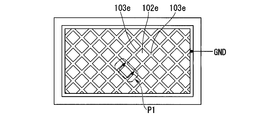
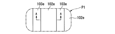
- FIG. 1A to 1D are diagrams schematically showing a transparent conductive substrate in the present embodiment
- FIG. 1A is an overall plan view
- FIG. 1B is an enlarged plan view of a region P1
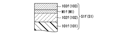
- FIGS. 1C and 1D are those in FIG. 1B.
- a cross-sectional view taken along line AA is shown.
- FIG. 1C is a cross-sectional view showing the transparent conductive substrate after etching
- FIG. 1D is a cross-sectional view showing the transparent conductive substrate before etching.
- the transparent conductive substrate in the present embodiment is disposed on a display panel such as a liquid crystal or organic EL (organic electroluminescence), and is used for a capacitive touch panel operated by touching an operation surface.
- a transparent conductive substrate is formed by sequentially laminating a transparent conductive film 102, an intermediate film M1, and a metal film 103 on a base 101 made of a flexible member.
- 1A to 1D show an example in which the metal film 103 has a mesh shape.
- the metal film 103e (103) disposed on the transparent conductive film 102e (102) has a mesh shape. Has been.
- the metal film 103e (103) is grounded to the external GND.
- the intermediate film M1 is provided at a position between the transparent conductive film 102 and the metal film 103 (the intermediate film M1 is omitted in FIGS. 1A and 1B).
- the intermediate film functions as an etching stopper layer when the metal film 103f having the entire surface formed film is etched to form the mesh-shaped metal film 103e in the manufacturing method described later.
- the substrate 101 is, for example, PET (polyethylene terephthalate), PP (polypropylene), PC (polycarbonate), COP (cycloolefin polymer: Cyclo-olefin polymer). ), PE (Polyethylene: Polyethylene), PMMA (Polymethyl methacrylate), etc., and flexible members such as substrates made of ultrathin glass having a plate thickness of 0.4 mm or less It is composed of A resin base has a problem that heat resistance is lower than that of a glass substrate.
- the substrate made of ultrathin glass has higher heat resistance than the resin-based substrate, but has a thin plate thickness, and may be greatly deformed during film formation due to heat input from the film formation source.
- the transparent conductive film 102 formed on the base 101 is an amorphous film.
- An amorphous film has a weaker property to etching than a crystalline film.
- a transparent conductive substrate S1f (S1) in which an intermediate film M1f is disposed so as to cover the transparent conductive film 102f and a metal film 103f is provided on the intermediate film M1f is provided.
- a mesh-like metal film 103e is formed by performing an etching process on the metal film 103f of the substrate S1f (S1) having such a configuration (FIG. 1C).
- the intermediate film in the above configuration is used by being disposed in a part of the transparent conductive substrate, that is, between the transparent conductive film and the metal film, it can ensure the conduction between the transparent conductive film and the metal film. It is required to have conductivity and high permeability. Specifically, a member having a property that the transmittance is 99 (%) or more is desired for the intermediate film. Further, the specific resistance value of the intermediate film depends on the transparent conductive film, metal film, material and thickness of the intermediate film, and the area to which each film is connected, but if it is 10000 ( ⁇ ⁇ cm) or less, the transparent conductive film It is sufficient to ensure conduction between the metal film and the metal film.
- the refractive index of the intermediate film is desirably equal to or less than the refractive index of the transparent conductive film.
- the intermediate film functions as an etching stopper layer, it is desirable that the intermediate film has resistance to an etching solution used when forming an opening in the metal film.
- the etching rate is desirably 1 nm / min.
- the intermediate film member that satisfies such conditions include Sn, Sn oxide, Sn oxide Sn alloy, Ti, Ti oxide, Ti oxide alloy, Nb, Nb oxide, and Nb oxide.
- an oxide containing Sn or an oxide containing Ti is preferable as a member of the intermediate film.
- the intermediate film is an oxide containing Sn
- the refractive index is close to that of ITO, which will be described later, which is a typical material for the transparent conductive film, and reflection occurs at the interface between the intermediate film and the transparent conductive film. It is more preferable because it is difficult.
- the oxide containing Sn means Sn oxide or Sn oxide alloy.
- an oxide containing Ti refers to oxidized Ti or oxidized Ti alloy.
- the metal film having the above structure is required to have excellent conductivity and high etching property.
- the metal film member that satisfies such conditions include Al, Al alloy, Mo, Mo alloy, Ti, Ti alloy, Cu, Cu alloy, and the like.
- transparent conductive film there is no restriction
- ITO tin tin oxide: Indium Tin Oxide
- AZO ZnO which doped Al
- BZO B-doped ZnO
- In 2 O 3 —TiO 2 and the like.
- Examples of the flexible member constituting the substrate in the above configuration include resin-based substrates such as PET, PP, PC, COP, PE, PMMA, and substrates made of ultrathin glass, as described above. .
- Step 1 "Transparent conductive substrate S1f in which transparent conductive film 102f / intermediate film M1f / metal film 103f are laminated in this order on flexible member 101f" using a sputtering apparatus (for example, FIG. 5) described later. It is formed and carried out into the air atmosphere (FIG. 2A).
- Step 2 In order to pattern the metal film 103f, a resist layer R patterned in a predetermined shape is formed on the surface of the metal film 103f (FIG. 2B).
- the transparent conductive substrate S1f on which the resist layer R is formed is also referred to as a processing object.
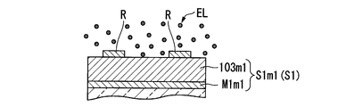
- Step 3 The etching solution EL is sprayed on the surface of the processing object S1m1 on which the resist layer is formed, and the portion of the metal film 103m1 exposed from the resist layer is etched (FIG. 2C). Instead of spraying, a method of immersing the processing object S1m1 in an etching solution may be used.
- Step 4 After a predetermined time, the etching is stopped (FIG. 2D). Spraying on the processing object S1m2 is stopped or the processing object S1m2 is pulled up from the etching solution. FIG. 2D shows the former case. At this time, the intermediate film is exposed in the region where the resist layer is not disposed.
- Step 5 After cleaning the processing object S1m2 and removing the etching solution, the transparent conductive substrate S1e (S1) according to the embodiment of the present invention is obtained by removing the resist layer.
- the method for manufacturing a transparent conductive substrate according to an embodiment of the present invention includes a step of providing a mask having a desired void pattern on the upper surface of the metal film and etching the metal film through the void pattern. Yes.
- the metal film can be etched by a desired pattern through the gap pattern provided in the mask until the intermediate film is exposed. Therefore, according to the embodiment of the present invention, it is possible to provide a method for manufacturing a transparent conductive substrate in which the intermediate film serves as a barrier, and damage to the transparent conductive film can be reliably prevented by etching.
- FIGS. 3A to 3D are views schematically showing another example of the transparent conductive substrate according to the embodiment of the present invention.
- FIG. 3A is an overall plan view
- FIG. 3B is an enlarged plan view of a region P2
- FIG. FIGS. 3D and 3D respectively show a cross-sectional view taken along line BB in FIG. 3B.
- FIG. 3C is a cross-sectional view showing the transparent conductive substrate after etching
- FIG. 3D is a cross-sectional view showing the transparent conductive substrate before etching.
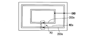
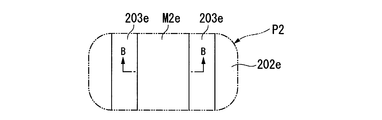
- the transparent conductive substrate S2 of FIGS. 3A to 3D is different from FIGS. 1A to 1D only in that the metal film 203 has a track shape by providing an opening on the intermediate film M2.
- FIGS. 3A to 3D show a configuration example in which two rounds of the track-shaped metal film 203 are arranged.
- the number of rounds of the metal film 203, the width of the round metal film 203, the separation distance, and the like are as follows. , Determined as needed. Also in this case, all the metal films 203e (203) are grounded to the external GND.
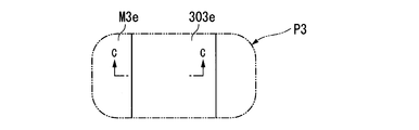
- FIG. 4A to 4D are diagrams schematically showing another example of the transparent conductive substrate according to the present invention.
- FIG. 4A is an overall plan view
- FIG. 4B is an enlarged plan view of a region P3
- FIGS. 4C and 4D Represents a cross-sectional view taken along line CC in FIG. 4B.
- FIG. 4C is a cross-sectional view showing the transparent conductive substrate after etching
- FIG. 4D is a cross-sectional view showing the transparent conductive substrate before etching.
- the transparent conductive substrate S3 of FIGS. 4A to 4D only the point that the metal film 303 is provided with an opening on the intermediate film M3 to form a frame shape including the end portion of the substrate. Different from FIG. 1D. 4A to 4D, the width and the like of the frame-shaped metal film 303 are determined as necessary. Also in this case, the metal film 303e (303) is grounded to the external GND.
- the transparent conductive substrate S1 prepared in Step 1 described above that is, “on the flexible member (PET film) 101f, transparent conductive film (ITO) 102f / intermediate film (GIT) M1f / metal film (Al ) 103f are sequentially laminated.
- a method for manufacturing the transparent conductive substrate S1f will be described.
- an interlock type sputtering apparatus as shown in FIG. 5 is used.
- the substrate 118 a (corresponding to the above-described base 101 made of a flexible member) is fed into a preparation / extraction chamber (L / UL) 111, heating chamber ( H) 112, first film formation chamber (S1) 113, first buffer chamber (B1) 114, second film formation chamber (S2) 115, second buffer chamber (B2) 116, third film formation chamber (S3)
- a preparation / extraction chamber L / UL
- H heating chamber
- first film formation chamber (S1) 113 first buffer chamber
- S2 second film formation chamber
- S3 second buffer chamber
- Partition valves DV1 to DV7 are arranged between the chambers, and buffer chambers are arranged between the film forming chambers. Independent film formation in first to third film forming spaces to be described later. It is comprised so that the atmosphere of conditions may be maintained. However, when the first to third film formation spaces described later are not affected by other film formation spaces (for example, a desired differential pressure mechanism or the like is disposed in the film formation space), a partition valve or The buffer chamber may be eliminated to form a single film formation space.
- the substrate 118a is transferred from the charging / unloading chamber 111 in a reduced pressure atmosphere to the heating chamber 112 and subjected to a desired heat treatment.
- the substrate 118b is degassed and heated to a desired temperature. Further, depending on the material of the substrate to be used, heat treatment for degassing may be unnecessary.
- the substrate 118b after the heat treatment is transferred from the heating chamber 112 to the first film formation chamber 113, and passes through the front of the target 113TG made of ITO (that is, the first film formation space sp1).
- a transparent conductive film (ITO) is formed on the substrate.
- the (Ar + O 2 ) mixed gas is supplied from the process gas supply source 113G to the first film formation space sp1, and a desired pressure is maintained by the exhaust device (exhaust means) 113P.
- a temperature adjusting device (temperature adjusting means) (not shown) may be installed to control the temperature of the substrate 118c during film formation.
- 113BP represents a backing plate on which the target 113TG is placed
- 113D represents a power source for supplying a high voltage to the backing plate 113BP.
- the substrate 118 c on which the transparent conductive film is formed is transferred from the first film formation chamber 113 to the first buffer chamber 114.
- the first buffer chamber 114 is disposed between the first film formation chamber 113 (first film formation space sp1) and a second film formation chamber 115 (second film formation space sp2), which will be described later.
- (Means) 114P maintains the desired degree of vacuum in the internal space of the first buffer chamber 114.
- the substrate 118c on which the transparent conductive film is formed is transferred from the first buffer chamber 114 to the second film formation chamber 115, and before the target 115TG made of the intermediate film base material (GIT) (that is, the second film formation chamber 115). It passes through the membrane space sp2). Thereby, an intermediate film (GIT) is formed on the transparent conductive film (ITO) of the substrate 118c.
- the (Ar + O 2 ) mixed gas is supplied from the process gas supply source 115G to the second film formation space sp2, and a desired pressure is maintained by the exhaust device (exhaust means) 115P.
- a temperature adjusting device (temperature adjusting means) (not shown) may be installed to control the temperature of the substrate 118c during film formation.
- 115BP represents a backing plate on which the target 115TG is placed
- 115D represents a power source for supplying a high voltage to the backing plate 115BP.
- the substrate 118d in which the intermediate film is laminated on the transparent conductive film is transferred from the second film formation chamber 115 to the second buffer chamber 116.
- the second buffer chamber 116 is disposed between the second film formation chamber 115 (second film formation space sp2) and a third film formation chamber 117 (third film formation space sp3) described later, and an exhaust device (exhaust gas).
- Means) 116P maintains a desired degree of vacuum in the internal space of the second buffer chamber 116.
- the substrate 118d in which the intermediate film is laminated on the transparent conductive film is transferred from the second buffer chamber 116 to the third film formation chamber 117, and in front of the target 117TG made of a metal film base material (Al) (that is, , Passes through the third film formation space sp3).
- a metal film (Al) is formed on the intermediate film of the substrate 118d.
- Ar gas is supplied from the process gas supply source 117G to the third film formation space sp3, and a desired pressure is maintained by the exhaust device (exhaust means) 117P.
- a temperature adjusting device (temperature adjusting means) (not shown) may be installed to control the temperature of the substrate 118d during film formation.
- 117BP represents a backing plate on which the target 117TG is placed
- 117D represents a power source for supplying a high voltage to the backing plate 117BP.
- the substrate 118 on which the transparent conductive film, the intermediate film, and the metal film are sequentially laminated is reversed (or reversely moved) as shown by an arrow RT in FIG. It is conveyed to the chamber 111 and taken out from the manufacturing apparatus to the outside (atmosphere). That is, the manufacturing apparatus shown in FIG. 5 has a first film formation space sp1 for forming the transparent conductive film, a second film formation space sp2 for forming the intermediate film, and a third film formation space for forming the metal film. at least sp3. In the direction in which the substrate moves, the second film formation space sp2 is disposed between the first film formation space sp1 and the third film formation space sp3.
- the transparent conductive substrate according to the embodiment of the present invention in which the desired patterning is performed on the metal film (Al) is obtained through the above-described etching process.
- Table 1 shows typical manufacturing conditions for the above-described transparent conductive film, intermediate film, and metal film oxide film.
- Table 2 shows typical etching process conditions when a mesh-like metal film is formed (FIGS. 1A to 1D and FIGS. 2A to 2D).
- a transparent conductive substrate provided with a mesh-like metal film as shown in FIGS. 1A to 1D can be stably produced.
- Typical production conditions for the transparent conductive film, the intermediate film, and the metal film oxide film as shown in Table 1 are not limited to the manufacturing apparatus shown in FIG. 5; for example, a multi-chamber type as shown in FIG. This can also be achieved with the manufacturing apparatus.
- FIG. 6 is a diagram schematically showing another example of the transparent conductive substrate manufacturing apparatus according to the present invention.
- the manufacturing apparatus of FIG. 6 corresponds to the case where the film forming steps of the transparent conductive film, the intermediate film, and the metal film oxide film are performed in independent film forming space chambers of separate film forming chambers (chambers).
- a substrate transport path made of a flexible base material in the case where each film forming step of a transparent conductive film, an intermediate film, and a metal film oxide film is performed using such a multi-chamber manufacturing apparatus will be described.
- the substrate is carried into the load chamber (L) 201 from the outside.
- the load chamber is transferred into the heating chamber (H) 202, and heat treatment (degassing treatment) is performed at a desired temperature.
- the heat-treated substrate is transferred from the heating chamber (H) 202 into the first film formation chamber (S1) 204A, and a transparent conductive film is formed in the first film formation space sp1.
- the substrate on which the transparent conductive film is formed is transferred from the first film formation chamber (S1) 204A into the second film formation chamber (S2) 204B, and an intermediate film is formed in the second film formation space sp2. Is called.
- the substrate on which the intermediate film is formed on the transparent conductive film is transferred from the second film formation chamber (S2) 204B into the third film formation chamber (S3) 205, and the metal film is formed in the third film formation space sp3. Film formation is performed.
- the substrate on which the intermediate film and the metal film are formed on the transparent conductive film is transferred from the third film formation chamber (S3) 205 to the unload chamber (UL) 206, and after waiting for a certain time, the unload chamber (UL) Unloaded from 206.
- a robot (not shown) installed in the transfer chamber (T) 207 is used as means for transporting the substrate between the chambers. Note that the chambers 201, 202, 204 A, 204 B, 205, and 206 including the transfer chamber (T) 207 are all under reduced pressure during process processing and transfer in each chamber.
- the manufacturing apparatus shown in FIG. 6 has a first film formation space sp1 for forming the transparent conductive film, a second film formation space sp2 for forming the intermediate film, and a third film formation space for forming the metal film. at least sp3.
- the second film formation space sp2 is disposed between the first film formation space sp1 and the third film formation space sp3.
- the present invention can be widely applied to a transparent conductive substrate, a manufacturing method thereof, and a transparent conductive substrate manufacturing apparatus.
- the transparent conductive substrate of the present invention is suitably used for a high-quality display screen that requires excellent visibility.
Landscapes
- Engineering & Computer Science (AREA)
- Chemical & Material Sciences (AREA)
- Theoretical Computer Science (AREA)
- General Engineering & Computer Science (AREA)
- General Physics & Mathematics (AREA)
- Physics & Mathematics (AREA)
- Materials Engineering (AREA)
- Chemical Kinetics & Catalysis (AREA)
- Mechanical Engineering (AREA)
- Metallurgy (AREA)
- Organic Chemistry (AREA)
- Human Computer Interaction (AREA)
- Microelectronics & Electronic Packaging (AREA)
- Manufacturing & Machinery (AREA)
- Manufacturing Of Electric Cables (AREA)
- Laminated Bodies (AREA)
- Shielding Devices Or Components To Electric Or Magnetic Fields (AREA)
- Non-Insulated Conductors (AREA)
Abstract
本発明の透明導電性基板は、可撓性部材からなる基体の一面に、透明導電膜、中間膜、金属膜が順に積層されてなる透明導電性基板であって、前記金属膜は1つ以上の開口部を備えており、前記中間膜が該開口部の底面を構成している。
Description
本発明は、透明導電性基板及びその製造方法、並びに、透明導電性基板の製造装置に係る。より詳細には、電磁波シールドと高い透過率とを併せ持つことが可能な電磁波遮蔽膜を備えた、透明導電性基板及びその製造方法、並びに、透明導電性基板の製造装置に関する。本発明は、タッチパネル用途などに好適である。
本願は、2015年4月24日に日本に出願された特願2015-089296号に基づき優先権を主張し、その内容をここに援用する。
本願は、2015年4月24日に日本に出願された特願2015-089296号に基づき優先権を主張し、その内容をここに援用する。
電磁波シールド技術は、従来、電磁波の影響を受けやすい、医療機器や計測機器、通信機器などにおいて広く利用されている。このような電磁波シールド技術は、最近、液晶に代表されるディスプレイ分野にも使用されているが、この分野においては、電磁波を遮断する機能に加えて、良好な光透過性も併せ持つことが求められている。このような傾向は、近年、表示装置と入力装置とが一体化したタッチパネルのような機器でも、高まってきている。
従来、光透過性を有する電磁波シールドとして、可撓性基材の全面に亘ってITO膜と金属膜とを順に配してなる構成(以下、ITO全面形成膜と呼ぶ)や、ガラス基材の全面に亘って設けられたITO膜上に金属部材の細線をメッシュ状に配してなる構成(以下、メタルメッシュと呼ぶ)が利用されていた。たとえば、前者の構成(ITO全面形成膜)は特許文献1に、後者の構成(メタルメッシュ)は特許文献2に、それぞれ開示されている。ここで、ITOは、酸化インジウム(Indium Tin Oxide)の略称であり、導電性と透過性を兼ね備えた材料(透明導電材料)の代表例である。
しかしながら、ITO全面形成膜を電磁波シールドとして利用する場合は、光透過性に優れるという長所がある反面、電磁シールドの性能としては、メタルメッシュに劣っていた。
これに対して、メタルメッシュを電磁波シールドとして利用する場合は、メッシュの配置等を工夫することによりシールド特性を向上できるという長所がある反面、光透過性が犠牲になったり、モアレが生じやすい等の問題を抱えていた。
これに対して、メタルメッシュを電磁波シールドとして利用する場合は、メッシュの配置等を工夫することによりシールド特性を向上できるという長所がある反面、光透過性が犠牲になったり、モアレが生じやすい等の問題を抱えていた。
そこで、上述した2つの構成における長所を併せ持つ構成、すなわち、ITO全面形成膜の上にメタルメッシュを積層して配する構成、を採用することにより、シールド特性(導電性)と光透過性とを両立させるための研究が進められている。
図7A~図7Dは、ITO全面形成膜の上にメタルメッシュを積層した構成の一例を示す図であり、図7Aは全体を示す平面図、図7Bは領域P5の拡大図、図7C及び図7Dは線分Z-Zにおける断面図を示している。図7A~図7Dにおいて、符号101は可撓性基材(基板)、符号102は透明導電膜、符号103は金属膜である。
図7A~図7Dは、ITO全面形成膜の上にメタルメッシュを積層した構成の一例を示す図であり、図7Aは全体を示す平面図、図7Bは領域P5の拡大図、図7C及び図7Dは線分Z-Zにおける断面図を示している。図7A~図7Dにおいて、符号101は可撓性基材(基板)、符号102は透明導電膜、符号103は金属膜である。
まず、透明導電膜102s上に金属膜103sを全面に形成する(図7D)。次いで、不図示のマスクを用い、金属膜103sに対してエッチング処理を施すことにより、メッシュ状の金属膜103eを得る(図7C)。ところが、メッシュ状の金属膜103eを形成する際に、その下地をなす透明導電膜102eまでエッチングされてしまい、金属膜103eの近傍にあたる透明導電膜102eが損傷し、深さDまで欠落した部位が生じてしまう傾向にあった。
このような欠落した部位が内在する透明導電膜102eにおいては、その膜中を流れる電流が局所的に不安定となる問題に加えて、十分な電流を確保するため、深さDの欠落部を見込み、余分な厚さを有する透明導電膜102sを予め形成しておく必要があった。
メッシュ状等の特定パターン形状からなる金属膜を形成する際に生じる、このような問題を解決する手法の開発が期待されていた。
メッシュ状等の特定パターン形状からなる金属膜を形成する際に生じる、このような問題を解決する手法の開発が期待されていた。
本発明は、上記の事情に鑑みてなされたもので、メッシュ状等の特定パターン形状からなる金属膜を形成する際に、その下地をなす透明導電膜がエッチングの影響を回避できる構成を備えた、透明導電性基板及びその製造方法、並びに、透明導電性基板の製造装置を提供することを目的とする。
本発明の第一態様に係る透明導電性基板は、可撓性部材からなる基体の一面に、透明導電膜、中間膜、金属膜が順に積層されてなる透明導電性基板であって、前記金属膜は1つ以上の開口部を備えており、前記中間膜が該開口部の底面を構成している。
本発明の第一態様に係る透明導電性基板においては、前記中間膜は、透過率が99(%)以上の部材で構成されてもよい。
本発明の第一態様に係る透明導電性基板においては、前記中間膜は、前記金属膜に開口部を形成する際に用いるエッチング液に対して、エッチング速度が1(nm/min)以下であってもよい。
本発明の第一態様に係る透明導電性基板においては、前記金属膜が、前記中間膜上において、前記開口部を備えることにより、メッシュ状に形成されてもよい。
本発明の第一態様に係る透明導電性基板においては、前記金属膜が、前記中間膜上において、前記開口部を備えることにより、トラック状に形成されてもよい。
本発明の第一態様に係る透明導電性基板においては、前記金属膜が、前記中間膜上において、前記開口部を備えることにより、額縁状に形成されてもよい。
本発明の第一態様に係る透明導電性基板においては、前記中間膜は、透過率が99(%)以上の部材で構成されてもよい。
本発明の第一態様に係る透明導電性基板においては、前記中間膜は、前記金属膜に開口部を形成する際に用いるエッチング液に対して、エッチング速度が1(nm/min)以下であってもよい。
本発明の第一態様に係る透明導電性基板においては、前記金属膜が、前記中間膜上において、前記開口部を備えることにより、メッシュ状に形成されてもよい。
本発明の第一態様に係る透明導電性基板においては、前記金属膜が、前記中間膜上において、前記開口部を備えることにより、トラック状に形成されてもよい。
本発明の第一態様に係る透明導電性基板においては、前記金属膜が、前記中間膜上において、前記開口部を備えることにより、額縁状に形成されてもよい。
本発明の第二態様に係る透明導電性基板の製造方法は、可撓性部材からなる基体の一面に、透明導電膜、中間膜、金属膜が順に積層されてなる透明導電性基板の製造方法であって、前記金属膜の上面に所望の空隙パターンを有するマスクを設けて、該空隙パターンを通して該金属膜をエッチング処理する工程を含む。
本発明の第三態様に係る透明導電性基板の製造装置は、可撓性部材からなる基体の一面に、透明導電膜、中間膜、金属膜が順に積層されてなる透明導電性基板の製造装置であって、前記透明導電膜を形成する第一成膜空間、前記中間膜を形成する第二成膜空間、及び、前記金属膜を形成する第三成膜空間を少なくとも備え、前記基体が移動する方向において、前記第二成膜空間が、前記第一成膜空間と前記第三成膜空間との間に配置されている。
本発明の第一態様に係る透明導電性基板は、可撓性部材からなる基体の一面に、透明導電膜、中間膜、金属膜が順に積層されているので、エッチングにより前記金属膜に形成された開口部(貫通孔)は、前記透明導電膜に至る前に必ず中間膜に達する。ゆえに、前記金属膜に形成された該開口部(貫通孔)の底面は中間膜となる。つまり、前記中間膜の存在により、前記透明導電膜は、前記金属膜に開口部(貫通孔)を形成するためのエッチングの影響を受けて損傷することがない。したがって、本発明の第一態様は、メッシュ状等の特定パターン形状からなる金属膜を形成する際に、その下地をなす透明導電膜がエッチングの影響を回避できる構成を備えた透明導電性基板の提供に貢献する。
上記構成における中間膜には、透明導電性基板の一部、すなわち、透明導電膜と金属膜の間に配置されて用いられることから、透明導電膜と金属膜との間の導通を確保するために必要な導電性と高い透過性が求められる。また、前記中間膜は、エッチング・ストッパー層として働くために、前記金属膜に開口部を形成する際に用いるエッチング液に対して、耐性を備えていることが望ましい。
本発明の第二態様に係る透明導電性基板の製造方法は、上記構成を得るために、可撓性部材/透明導電膜/中間膜/金属膜が順に積層されてなる透明導電性基板を用い、前記金属膜の上面に所望の空隙パターンを有するマスクを設けて、該空隙パターンを通して該金属膜をエッチング処理する工程を含んでいる。これにより、マスクに設けた空隙パターンを通して、所望のパターンで、中間膜が露呈するまで金属膜をエッチング処理できる。ゆえに、本発明の第二態様によれば、中間膜が障壁となり、エッチングにより透明導電膜の損傷を確実に防止できる、透明導電性基板の製造方法の提供が可能となる。
本発明の第三態様に係る透明導電性基板の製造装置は、上記構成を得るために、可撓性部材からなる基体の上に透明導電膜、中間膜、金属膜が順に積層されてなる透明導電性基板を作製することが求められる。このような層構成の透明導電性基板を作製するためには、前記透明導電膜を形成する第一成膜空間、前記中間膜を形成する第二成膜空間、及び、前記金属膜を形成する第三成膜空間を少なくとも備えるとともに、前記基体が移動する方向において、前記第二成膜空間が、前記第一成膜空間と前記第三成膜空間との間に配置されている製造装置が好適である。その際、各成膜空間は独立した成膜室が配置される構成の他に、他の成膜空間に影響を及ぼさない工夫が成されていれば、たとえば単一の連続した空間を構成していてもよい。また、前記3つの成膜空間以外に、必要に応じて他の空間が配置される構成としても構わない。
以下、本発明に係る透明導電性基板の一実施形態を、図面に基づいて説明する。
<第一実施形態>
図1A~図1Dは、本実施形態における透明導電性基板を模式的に示す図であり、図1Aは全体平面図、図1Bは領域P1の拡大平面図、図1C及び図1Dは図1Bにおける線分A-Aの断面図、を各々表している。特に、図1Cは、エッチング後の透明導電性基板を示す断面図であり、図1Dは、エッチング前の透明導電性基板を示す断面図である。
<第一実施形態>
図1A~図1Dは、本実施形態における透明導電性基板を模式的に示す図であり、図1Aは全体平面図、図1Bは領域P1の拡大平面図、図1C及び図1Dは図1Bにおける線分A-Aの断面図、を各々表している。特に、図1Cは、エッチング後の透明導電性基板を示す断面図であり、図1Dは、エッチング前の透明導電性基板を示す断面図である。
本実施形態における透明導電性基板は、たとえば液晶や有機EL(有機エレクトロルミネッセンス)などの表示パネル上に配置され、操作面に触って操作される静電容量方式のタッチパネルなどに用いられる。
このような透明導電性基板は、図1A~図1Dに示すように、可撓性部材からなる基体101の上に透明導電膜102、中間膜M1、金属膜103が順に積層されてなる。図1A~図1Dは金属膜103がメッシュ状をなす一例であり、図1Aに示すように、透明導電膜102e(102)の上に配された金属膜103e(103)がメッシュ状の形状とされている。この金属膜103e(103)は、外部のGNDに接地される。
このような透明導電性基板は、図1A~図1Dに示すように、可撓性部材からなる基体101の上に透明導電膜102、中間膜M1、金属膜103が順に積層されてなる。図1A~図1Dは金属膜103がメッシュ状をなす一例であり、図1Aに示すように、透明導電膜102e(102)の上に配された金属膜103e(103)がメッシュ状の形状とされている。この金属膜103e(103)は、外部のGNDに接地される。
本発明の実施形態では、中間膜M1が透明導電膜102と金属膜103に挟まれる位置に設けられている(図1A及び図1Bでは中間膜M1は省略)。この中間膜は、後述する製造方法において、全面形成膜状の金属膜103fをエッチングして、メッシュ状の金属膜103eを形成する際に、エッチング・ストッパー層として機能する。
本実施形態の透明導電性基板において、基体101は、たとえば、PET(ポリエチレンテレフタレート:polyethylene terephthalate)、PP(プリプロピレン:polypropylene)、PC(ポリカーボネート:polycarbonate)、COP(シクロオレフィンポリマー:Cyclo-olefin polymer)、PE(polyethylene:ポリエチレン)、PMMA(Polymethyl methacrylate:ポリメタクリル酸メチル)、等の樹脂系基体や、0.4mm以下の板厚を有する極薄のガラスからなる基体、等の可撓性部材から構成されている。樹脂系基体は、ガラス基板に比べると耐熱性が低いという問題がある。これに対して、極薄のガラスからなる基体は、耐熱性は樹脂系基体よりも高いが、板厚が薄いため、成膜源からの入熱により成膜中に大きく変形する虞がある。
それゆえ、基体101上に透明導電膜102を作製する際の基板温度は低温に保つ必要があるため、基体101上に形成される透明導電膜102はアモルファス膜となる。アモルファス膜は結晶膜に比べてエッチングに弱い性質がある。これを解消するため、本発明の実施形態では透明導電膜102fを覆うように中間膜M1fを配置して、該中間膜M1fの上に金属膜103fを設けた透明導電性基板S1f(S1)を用意した(図1D)。このような構成とした基板S1f(S1)の金属膜103fに対して、エッチング処理を施すことにより、本実施形態ではメッシュ状の金属膜103eを形成した(図1C)。
上記構成における中間膜は、透明導電性基板の一部、すなわち、透明導電膜と金属膜の間、に配置されて用いられることから、透明導電膜と金属膜との間の導通を確保できるだけの導電性と高い透過性を持つことが求められる。具体的には、中間膜には、透過率が99(%)以上の特性を備えた部材が望まれる。
また、中間膜の比抵抗値は、透明導電膜や金属膜、中間膜の材質や膜厚、各膜が接続する面積にもよるが、10000(μΩ・cm)以下であれば、透明導電膜と金属膜との間の導通の確保に十分である。
また、中間膜の比抵抗値は、透明導電膜や金属膜、中間膜の材質や膜厚、各膜が接続する面積にもよるが、10000(μΩ・cm)以下であれば、透明導電膜と金属膜との間の導通の確保に十分である。
さらに、透明導電膜と中間膜との間での反射を抑えるために、中間膜の屈折率は透明導電膜の屈折率の同等以下であることが望ましい。さらに、前記中間膜は、エッチング・ストッパー層として働くために、前記金属膜に開口部を形成する際に用いるエッチング液に対して、耐性を備えていることが望ましい。具体的には、エッチング・レートが1nm/minであることが望ましい。このような条件を満たす中間膜の部材としては、たとえば、Sn、酸化Sn、酸化Sn合金、Ti、酸化Ti、酸化Ti合金、Nb、酸化Nb、酸化Nb合金、等が挙げられる。
ここで、抵抗値を低くできるという点から、Snを含む酸化物やTiを含む酸化物が、中間膜の部材として好ましい。特に、中間膜がSnを含む酸化物の場合には、透明導電膜として代表的な材料である後述のITOに対して屈折率の値が近く、中間膜と透明導電膜の界面において反射が起きにくいと言う点から、より好ましい。本発明の実施形態において、Snを含む酸化物とは、酸化Snや酸化Sn合金を意味する。同様に、Tiを含む酸化物とは、酸化Tiや酸化Ti合金を指す。
上記構成における金属膜には、優れた導電性と高いエッチング性が求められる。このような条件を満たす金属膜の部材としては、たとえば、Al、Al合金、Mo、Mo合金、Ti、Ti合金、Cu、Cu合金、等が挙げられる。
上記構成における透明導電膜としては、特に制限はなく、公知の透明導電材料を用いることが可能であり、たとえば、ITO(スズドープ酸化インジウム:Indium Tin Oxide)、AZO(AlをドープしたZnO)、BZO(BをドープしたZnO)、InO2-ZnO、In2O3-TiO2、等が挙げられる。
上記構成における基材を構成する可撓性部材としては、前述したとおり、PET、PP、PC、COP、PE、PMMA、等の樹脂系基体や、極薄のガラスからなる基体、等が挙げられる。
図2A~図2Eは、本発明に係る透明導電性基板の製造方法を模式的に示す図であり、特に金属膜のパターニングを行うためのエッチング工程を詳細に示している。以下では、図2A~図2Eを参照して、上述した構成の透明導電性基板を作製する方法を説明する。
工程1:後述するスパッタリング装置(たとえば図5)を用いて、「可撓性部材101f上に、透明導電膜102f/中間膜M1f/金属膜103fが順に積層されてなる透明導電性基板S1f」を形成し、大気雰囲気中に搬出する(図2A)。
工程2:金属膜103fのパターニングを行うために、金属膜103fの表面に所定形状にパターニングされたレジスト層Rを形成する(図2B)。以下では、レジスト層Rを形成した透明導電性基板S1fのことを、処理対象物とも呼ぶ。
工程1:後述するスパッタリング装置(たとえば図5)を用いて、「可撓性部材101f上に、透明導電膜102f/中間膜M1f/金属膜103fが順に積層されてなる透明導電性基板S1f」を形成し、大気雰囲気中に搬出する(図2A)。
工程2:金属膜103fのパターニングを行うために、金属膜103fの表面に所定形状にパターニングされたレジスト層Rを形成する(図2B)。以下では、レジスト層Rを形成した透明導電性基板S1fのことを、処理対象物とも呼ぶ。
工程3:処理対象物S1m1のレジスト層を形成した面にエッチング液ELを噴霧し、レジスト層から露出した金属膜103m1の部位をエッチングする(図2C)。噴霧に代えて、処理対象物S1m1を、エッチング液に浸漬する方法を用いてもよい。
工程4:所定時間後、エッチングを停止する(図2D)。処理対象物S1m2に帯する噴霧を停止するか、エッチング液から処理対象物S1m2を引き上げる。図2Dは前者の場合を表している。このとき、レジスト層が配置されていなかった領域では、中間膜が露呈された状態となる。
工程5:処理対象物S1m2を洗浄しエッチング液を除去した後、レジスト層を取り除くことにより、本発明の実施形態に係る透明導電性基板S1e(S1)が得られる。
工程4:所定時間後、エッチングを停止する(図2D)。処理対象物S1m2に帯する噴霧を停止するか、エッチング液から処理対象物S1m2を引き上げる。図2Dは前者の場合を表している。このとき、レジスト層が配置されていなかった領域では、中間膜が露呈された状態となる。
工程5:処理対象物S1m2を洗浄しエッチング液を除去した後、レジスト層を取り除くことにより、本発明の実施形態に係る透明導電性基板S1e(S1)が得られる。
すなわち、本発明の実施形態に係る透明導電性基板の製造方法は、前記金属膜の上面に所望の空隙パターンを有するマスクを設けて、該空隙パターンを通して該金属膜をエッチング処理する工程を含んでいる。これにより、マスクに設けた空隙パターンを通して、所望のパターンで、中間膜が露呈するまで金属膜をエッチング処理できる。ゆえに、本発明の実施形態によれば、中間膜が障壁となり、エッチングにより透明導電膜の損傷を確実に防止できる、透明導電性基板の製造方法の提供が可能となる。
<第二実施形態>
図3A~図3Dは、本発明の実施形態に係る透明導電性基板の他の一例を模式的に示す図であり、図3Aは全体平面図、図3Bは領域P2の拡大平面図、図3C及び図3Dは図3Bにおける線分B-Bの断面図、を各々表している。特に、図3Cは、エッチング後の透明導電性基板を示す断面図であり、図3Dは、エッチング前の透明導電性基板を示す断面図である。
図3A~図3Dの透明導電性基板S2では、金属膜203が、中間膜M2上において、開口部を備えることにより、トラック状を形成している点のみ、図1A~図1Dと異なる。図3A~図3Dは、周回するトラック状の金属膜203が2周分配置された構成例を示しているが、金属膜203の周回数や、周回する金属膜203の幅、離間距離等は、必要に応じて決定される。この場合も、金属膜203e(203)は全て、外部のGNDに接地される。
図3A~図3Dは、本発明の実施形態に係る透明導電性基板の他の一例を模式的に示す図であり、図3Aは全体平面図、図3Bは領域P2の拡大平面図、図3C及び図3Dは図3Bにおける線分B-Bの断面図、を各々表している。特に、図3Cは、エッチング後の透明導電性基板を示す断面図であり、図3Dは、エッチング前の透明導電性基板を示す断面図である。
図3A~図3Dの透明導電性基板S2では、金属膜203が、中間膜M2上において、開口部を備えることにより、トラック状を形成している点のみ、図1A~図1Dと異なる。図3A~図3Dは、周回するトラック状の金属膜203が2周分配置された構成例を示しているが、金属膜203の周回数や、周回する金属膜203の幅、離間距離等は、必要に応じて決定される。この場合も、金属膜203e(203)は全て、外部のGNDに接地される。
<第三実施形態>
図4A~図4Dは、本発明に係る透明導電性基板の他の一例を模式的に示す図であり、図4Aは全体平面図、図4Bは領域P3の拡大平面図、図4C及び図4Dは図4Bにおける線分C-Cの断面図、を各々表している。特に、図4Cは、エッチング後の透明導電性基板を示す断面図であり、図4Dは、エッチング前の透明導電性基板を示す断面図である。
図4A~図4Dの透明導電性基板S3では、金属膜303が、中間膜M3上において、開口部を備えることにより、基体の端部を含む額縁状を形成している点のみ、図1A~図1Dと異なる。図4A~図4Dにおいて、額縁状の金属膜303の幅等は、必要に応じて決定される。この場合も、金属膜303e(303)は、外部のGNDに接地される。
図4A~図4Dは、本発明に係る透明導電性基板の他の一例を模式的に示す図であり、図4Aは全体平面図、図4Bは領域P3の拡大平面図、図4C及び図4Dは図4Bにおける線分C-Cの断面図、を各々表している。特に、図4Cは、エッチング後の透明導電性基板を示す断面図であり、図4Dは、エッチング前の透明導電性基板を示す断面図である。
図4A~図4Dの透明導電性基板S3では、金属膜303が、中間膜M3上において、開口部を備えることにより、基体の端部を含む額縁状を形成している点のみ、図1A~図1Dと異なる。図4A~図4Dにおいて、額縁状の金属膜303の幅等は、必要に応じて決定される。この場合も、金属膜303e(303)は、外部のGNDに接地される。
<透明導電膜、中間膜及び金属膜の作製方法>
以下では、上述した工程1で用意した透明導電性基板S1、すなわち、「可撓性部材(PETフィルム)101f上に、透明導電膜(ITO)102f/中間膜(GIT)M1f/金属膜(Al)103fが順に積層されてなる」透明導電性基板S1f、の作製方法について説明する。
以下では、上述した工程1で用意した透明導電性基板S1、すなわち、「可撓性部材(PETフィルム)101f上に、透明導電膜(ITO)102f/中間膜(GIT)M1f/金属膜(Al)103fが順に積層されてなる」透明導電性基板S1f、の作製方法について説明する。
可撓性部材からなる基体101上に、透明導電膜、中間膜及び金属膜を形成するための製造装置としては、たとえば図5に示すようなインターバック式のスパッタリング装置が用いられる。
図5の製造装置においては、基板118a(上述した可撓性部材からなる基体101に相当)は、不図示の搬送装置(搬送手段)により、仕込取出室(L/UL)111、加熱室(H)112、第一成膜室(S1)113、第一バッファ室(B1)114、第二成膜室(S2)115、第二バッファ室(B2)116、第三成膜室(S3)117の内部を移動可能とされている。
各室の間には、仕切りバルブDV1~DV7が配置されており、また各成膜室の間にはバッファ室が配置されており、後述する第一乃至第三成膜空間において独立した成膜条件の雰囲気が維持されるように構成されている。ただし、後述する第一乃至第三成膜空間が、他の成膜空間の影響が及ぶことが無い場合(たとえば、所望の差圧機構等を成膜空間内に配置)には、仕切りバルブやバッファ室を排除して、単一の成膜空間としても構わない。
まず、基板118aは減圧雰囲気とされた仕込取出室111から加熱室112へ搬送され、所望の熱処理が施される。この熱処理により、基板118bは、脱ガスされるとともに、所望の温度に加熱された状態になる。また、使用する基板の材質によっては、脱ガスのための熱処理は不要とすることができる。
次に、熱処理後の基板118bは、加熱室112から第一成膜室113へ搬送され、ITOからなるターゲット113TGの前(すなわち、第一成膜空間sp1)を通過させることにより、基板118c上に透明導電膜(ITO)を形成する。その際、第一成膜空間sp1には、プロセスガスの供給源113Gから(Ar+O2)混合ガスが供給され、排気装置(排気手段)113Pにより所望の圧力が維持される。必要に応じて、不図示の温度調整装置(温度調整手段)を設置して、成膜中の基板118cの温度を制御してもよい。113BPはターゲット113TGを載置するバッキングプレートを、113Dはバッキングプレート113BPに高電圧を供給する電源を、それぞれ表している。
その後、透明導電膜が形成された基板118cは、第一成膜室113から第一バッファ室114へ搬送される。第一バッファ室114は第一成膜室113(第一成膜空間sp1)と後述する第二成膜室115(第二成膜空間sp2)との間に配されており、排気装置(排気手段)114Pにより、第一バッファ室114の内部空間は所望の真空度が保持されている。第一バッファ室114内の位置αに、透明導電膜が形成された基板118cを所望の時間だけ滞在させることにより、前段の第一成膜空間sp1と後段の第二成膜空間sp2とが互いに影響し合うことが防止される。
次に、透明導電膜が形成された基板118cは、第一バッファ室114から第二成膜室115へ搬送され、中間膜の母材(GIT)からなるターゲット115TGの前(すなわち、第二成膜空間sp2)を通過する。これにより、基板118cの透明導電膜(ITO)上に中間膜(GIT)を形成する。その際、第二成膜空間sp2には、プロセスガスの供給源115Gから(Ar+O2)混合ガスが供給され、排気装置(排気手段)115Pにより所望の圧力が維持される。必要に応じて、不図示の温度調整装置(温度調整手段)を設置して、成膜中の基板118cの温度を制御してもよい。115BPはターゲット115TGを載置するバッキングプレートを、115Dはバッキングプレート115BPに高電圧を供給する電源を、それぞれ表している。
その後、透明導電膜上に中間膜が積層された基板118dは、第二成膜室115から第二バッファ室116へ搬送される。第二バッファ室116は第二成膜室115(第二成膜空間sp2)と後述する第三成膜室117(第三成膜空間sp3)との間に配されており、排気装置(排気手段)116Pにより、第二バッファ室116の内部空間は所望の真空度が保持されている。第二バッファ室116内の位置βに、中間膜が形成された基板118dを所望の時間だけ滞在させることにより、前段の第二成膜空間sp2と後段の第三成膜空間sp3とが互いに影響し合うことが防止される。
次に、透明導電膜上に中間膜が積層された基板118dは、第二バッファ室116から第三成膜室117へ搬送され、金属膜の母材(Al)からなるターゲット117TGの前(すなわち、第三成膜空間sp3)を通過する。これにより、基板118dの中間膜上に金属膜(Al)を形成する。その際、第三成膜空間sp3には、プロセスガスの供給源117GからArガスが供給され、排気装置(排気手段)117Pにより所望の圧力が維持される。必要に応じて、不図示の温度調整装置(温度調整手段)を設置して、成膜中の基板118dの温度を制御してもよい。117BPはターゲット117TGを載置するバッキングプレートを、117Dはバッキングプレート117BPに高電圧を供給する電源を、それぞれ表している。
そして、透明導電膜と中間膜と金属膜が順に積層形成された基板118は、図5に矢印RTで示すように、反転(あるいは逆走)させることにより、第三成膜室117から仕込取出室111へ搬送され、製造装置から外部(大気雰囲気)へ取り出される。
つまり、図5に示す製造装置は、前記透明導電膜を形成する第一成膜空間sp1、前記中間膜を形成する第二成膜空間sp2、及び、前記金属膜を形成する第三成膜空間sp3を少なくとも備えている。前記基体が移動する方向において、前記第二成膜空間sp2が、前記第一成膜空間sp1と前記第三成膜空間sp3との間に配置されている。
つまり、図5に示す製造装置は、前記透明導電膜を形成する第一成膜空間sp1、前記中間膜を形成する第二成膜空間sp2、及び、前記金属膜を形成する第三成膜空間sp3を少なくとも備えている。前記基体が移動する方向において、前記第二成膜空間sp2が、前記第一成膜空間sp1と前記第三成膜空間sp3との間に配置されている。
次いで、上述したエッチング工程を経ることにより、金属膜(Al)に対して所望のパターニングが施された、本発明の実施形態に係る透明導電性基板が得られる。
上述した透明導電膜と中間膜と金属膜酸化膜の代表的な作製条件を表1に示す。また、メッシュ状の金属膜を形成する場合(図1A~図1D及び図2A~図2D)の代表的なエッチング工程の処理条件を表2に示す。
上述した透明導電膜と中間膜と金属膜酸化膜の代表的な作製条件を表1に示す。また、メッシュ状の金属膜を形成する場合(図1A~図1D及び図2A~図2D)の代表的なエッチング工程の処理条件を表2に示す。


表1および表2の条件により、図1A~図1Dに示すようなメッシュ状の金属膜を備えた透明導電性基板を安定して作製することができる。
表1に示すような、透明導電膜と中間膜と金属膜酸化膜の代表的な作製条件は、図5の製造装置に限定されるものではなく、たとえば、図6に示すようなマルチチャンバ型の製造装置でも達成することができる。
表1に示すような、透明導電膜と中間膜と金属膜酸化膜の代表的な作製条件は、図5の製造装置に限定されるものではなく、たとえば、図6に示すようなマルチチャンバ型の製造装置でも達成することができる。
図6は、本発明に係る透明導電性基板の製造装置の他の一例を模式的に示す図である。図6の製造装置は、透明導電膜と中間膜と金属膜酸化膜の各成膜工程が、別々の成膜室(チャンバ)の独立した成膜空間室内において行われる場合に対応している。
このようなマルチチャンバの製造装置を用いて、透明導電膜と中間膜と金属膜酸化膜の各成膜工程を行う場合における、可撓性基材からなる基板の搬送経路について説明する。
まず、基板は、外部からロード室(L)201に搬入される。そして、ロード室において減圧下で一定時間待機した後に、加熱室(H)202内に搬送され、所望の温度にて熱処理(脱ガス処理)が行われる。
まず、基板は、外部からロード室(L)201に搬入される。そして、ロード室において減圧下で一定時間待機した後に、加熱室(H)202内に搬送され、所望の温度にて熱処理(脱ガス処理)が行われる。
次に、加熱処理された基板は、加熱室(H)202から第一成膜室(S1)204A内に搬送され、第一成膜空間sp1において透明導電膜の成膜が行われる。その後、透明導電膜が形成された基板は、第一成膜室(S1)204Aから第二成膜室(S2)204B内に搬送され、第二成膜空間sp2において中間膜の成膜が行われる。さらに、透明導電膜上に中間膜が形成された基板は、第二成膜室(S2)204Bから第三成膜室(S3)205内に搬送され、第三成膜空間sp3において金属膜の成膜が行われる。
続いて、透明導電膜上に中間膜、金属膜が形成された基板は、第三成膜室(S3)205からアンロード室(UL)206に搬送され、一定時間待機した後に、アンロード室(UL)206から外部へ搬出される。各室間の間で基板を搬送する手段としては、トランスファ室(T)207に設置されたロボット(不図示)が用いられる。なお、各室においてプロセス処理中および搬送中は、トランスファ室(T)207を含めて各室201、202、204A、204B、205、206は全て減圧下にある。
つまり、図6に示す製造装置は、前記透明導電膜を形成する第一成膜空間sp1、前記中間膜を形成する第二成膜空間sp2、及び、前記金属膜を形成する第三成膜空間sp3を少なくとも備えている。前記基体が移動する方向において、前記第二成膜空間sp2が、前記第一成膜空間sp1と前記第三成膜空間sp3との間に配置されている。
本発明は、透明導電性基板及びその製造方法、並びに、透明導電性基板の製造装置に広く適用可能である。本発明の透明導電性基板は、優れた視認性が求められる高品位な表示画面などに好適に用いられる。
M1(M1e、M1f) 中間膜、P1 領域、S1(S1e、S1f) 透明導電性基板、101(101e、101f) 基体、102(102e、102f) 透明導電膜、103(103e、103f) 金属膜。
Claims (8)
- 可撓性部材からなる基体の一面に、透明導電膜、中間膜、金属膜が順に積層されてなる透明導電性基板であって、
前記金属膜は1つ以上の開口部を備えており、前記中間膜が該開口部の底面を構成している透明導電性基板。 - 前記中間膜は、透過率が99(%)以上の部材からなる請求項1に記載の透明導電性基板。
- 前記中間膜は、前記金属膜に開口部を形成する際に用いるエッチング液に対して、エッチング速度が1(nm/min)以下である請求項1に記載の透明導電性基板。
- 前記金属膜は、前記中間膜上において、前記開口部を備えることにより、メッシュ状に形成されている請求項1から請求項3のいずれか一項に記載の透明導電性基板。
- 前記金属膜は、前記中間膜上において、前記開口部を備えることにより、トラック状に形成されている請求項1から請求項3のいずれか一項に記載の透明導電性基板。
- 前記金属膜は、前記中間膜上において、前記開口部を備えることにより、額縁状に形成されている請求項1から請求項3のいずれか一項に記載の透明導電性基板。
- 可撓性部材からなる基体の一面に、透明導電膜、中間膜、金属膜が順に積層されてなる透明導電性基板の製造方法であって、
前記金属膜の上面に所望の空隙パターンを有するマスクを設けて、該空隙パターンを通して該金属膜をエッチング処理する工程を含む透明導電性基板の製造方法。 - 可撓性部材からなる基体の一面に、透明導電膜、中間膜、金属膜が順に積層されてなる透明導電性基板の製造装置であって、
前記透明導電膜を形成する第一成膜空間、前記中間膜を形成する第二成膜空間、及び、前記金属膜を形成する第三成膜空間を少なくとも備え、
前記基体が移動する方向において、前記第二成膜空間が、前記第一成膜空間と前記第三成膜空間との間に配置されている透明導電性基板の製造装置。
Priority Applications (1)
| Application Number | Priority Date | Filing Date | Title |
|---|---|---|---|
| JP2017514109A JP6293368B2 (ja) | 2015-04-24 | 2016-04-18 | 透明導電性基板及びその製造方法、並びに、透明導電性基板の製造装置 |
Applications Claiming Priority (2)
| Application Number | Priority Date | Filing Date | Title |
|---|---|---|---|
| JP2015089296 | 2015-04-24 | ||
| JP2015-089296 | 2015-04-24 |
Publications (1)
| Publication Number | Publication Date |
|---|---|
| WO2016171097A1 true WO2016171097A1 (ja) | 2016-10-27 |
Family
ID=57144099
Family Applications (1)
| Application Number | Title | Priority Date | Filing Date |
|---|---|---|---|
| PCT/JP2016/062232 Ceased WO2016171097A1 (ja) | 2015-04-24 | 2016-04-18 | 透明導電性基板及びその製造方法、並びに、透明導電性基板の製造装置 |
Country Status (3)
| Country | Link |
|---|---|
| JP (1) | JP6293368B2 (ja) |
| TW (1) | TW201644356A (ja) |
| WO (1) | WO2016171097A1 (ja) |
Citations (3)
| Publication number | Priority date | Publication date | Assignee | Title |
|---|---|---|---|---|
| JP2009301830A (ja) * | 2008-06-12 | 2009-12-24 | Nitto Denko Corp | 透明導電性フィルム、透明導電性積層体及びタッチパネル |
| JP2013001009A (ja) * | 2011-06-17 | 2013-01-07 | Nitto Denko Corp | 導電性積層体、パターン配線付き透明導電性積層体、および光学デバイス。 |
| JP2013228782A (ja) * | 2012-04-24 | 2013-11-07 | Gunze Ltd | 導電性基板、タッチパネル、および導電性基板の製造方法 |
Family Cites Families (2)
| Publication number | Priority date | Publication date | Assignee | Title |
|---|---|---|---|---|
| JP2010139641A (ja) * | 2008-12-10 | 2010-06-24 | Canon Inc | 表示装置 |
| JP5676214B2 (ja) * | 2010-11-04 | 2015-02-25 | ユー・ディー・シー アイルランド リミテッド | 有機電界発光装置 |
-
2016
- 2016-04-18 WO PCT/JP2016/062232 patent/WO2016171097A1/ja not_active Ceased
- 2016-04-18 JP JP2017514109A patent/JP6293368B2/ja active Active
- 2016-04-21 TW TW105112466A patent/TW201644356A/zh unknown
Patent Citations (3)
| Publication number | Priority date | Publication date | Assignee | Title |
|---|---|---|---|---|
| JP2009301830A (ja) * | 2008-06-12 | 2009-12-24 | Nitto Denko Corp | 透明導電性フィルム、透明導電性積層体及びタッチパネル |
| JP2013001009A (ja) * | 2011-06-17 | 2013-01-07 | Nitto Denko Corp | 導電性積層体、パターン配線付き透明導電性積層体、および光学デバイス。 |
| JP2013228782A (ja) * | 2012-04-24 | 2013-11-07 | Gunze Ltd | 導電性基板、タッチパネル、および導電性基板の製造方法 |
Also Published As
| Publication number | Publication date |
|---|---|
| JPWO2016171097A1 (ja) | 2017-11-02 |
| TW201644356A (zh) | 2016-12-16 |
| JP6293368B2 (ja) | 2018-03-14 |
Similar Documents
| Publication | Publication Date | Title |
|---|---|---|
| JP7495964B2 (ja) | 表示装置 | |
| JP7737510B2 (ja) | 発光装置 | |
| KR20220146373A (ko) | 표시 장치 및 전자 기기 | |
| JP2021177253A (ja) | 表示パネル、及び電子機器 | |
| US10090326B2 (en) | Flexible display substrate and a manufacturing method thereof, as well as a flexible display device | |
| CN108573981B (zh) | 显示基板及其制备方法、显示装置 | |
| TWI691089B (zh) | 薄膜電晶體、製造該薄膜電晶體的方法及包含該薄膜電晶體的顯示裝置 | |
| CN107526468B (zh) | 显示屏及其制备方法 | |
| US10473965B2 (en) | Array substrate and its manufacturing method and display panel | |
| KR102293981B1 (ko) | 유기발광표시패널 및 그 제조방법 | |
| WO2016201926A1 (en) | Substrate, touch display panel having the same, and manufacturing method thereof | |
| CN110534549A (zh) | 阵列基板、显示面板及阵列基板的制作方法 | |
| US9446571B2 (en) | Touch panel and method of manufacturing touch panel | |
| CN106972033A (zh) | 阵列基板及其制造方法、显示面板和显示装置 | |
| WO2016101495A1 (zh) | 制作触摸面板的方法、触摸面板、触摸屏和显示装置 | |
| KR20160048154A (ko) | 입력 장치에 사용되는 전극, 및 그 제조 방법 | |
| TW201403419A (zh) | 觸控面板及其製造方法 | |
| CN107250959B (zh) | 透明导电性基板及透明层叠结构体 | |
| JP6293368B2 (ja) | 透明導電性基板及びその製造方法、並びに、透明導電性基板の製造装置 | |
| CN103500746A (zh) | 阵列基板及其制备方法、显示装置 | |
| KR20140090876A (ko) | 다층 구조의 투명 전극 | |
| CN105677123B (zh) | 一种触控面板及其制作方法、显示装置 | |
| CN114388709B (zh) | 显示面板及其制作方法和显示装置 | |
| JP6497744B2 (ja) | タッチパネル | |
| CN104218059A (zh) | 显示装置和制造显示装置的方法 |
Legal Events
| Date | Code | Title | Description |
|---|---|---|---|
| 121 | Ep: the epo has been informed by wipo that ep was designated in this application |
Ref document number: 16783118 Country of ref document: EP Kind code of ref document: A1 |
|
| ENP | Entry into the national phase |
Ref document number: 2017514109 Country of ref document: JP Kind code of ref document: A |
|
| NENP | Non-entry into the national phase |
Ref country code: DE |
|
| 122 | Ep: pct application non-entry in european phase |
Ref document number: 16783118 Country of ref document: EP Kind code of ref document: A1 |