WO2016171069A1 - 表示制御装置、液晶表示装置、表示制御プログラム及び記録媒体 - Google Patents
表示制御装置、液晶表示装置、表示制御プログラム及び記録媒体 Download PDFInfo
- Publication number
- WO2016171069A1 WO2016171069A1 PCT/JP2016/062023 JP2016062023W WO2016171069A1 WO 2016171069 A1 WO2016171069 A1 WO 2016171069A1 JP 2016062023 W JP2016062023 W JP 2016062023W WO 2016171069 A1 WO2016171069 A1 WO 2016171069A1
- Authority
- WO
- WIPO (PCT)
- Prior art keywords
- display
- voltage
- gradation
- frame
- unit
- Prior art date
- Legal status (The legal status is an assumption and is not a legal conclusion. Google has not performed a legal analysis and makes no representation as to the accuracy of the status listed.)
- Ceased
Links
Images


Classifications
-
- G—PHYSICS
- G09—EDUCATION; CRYPTOGRAPHY; DISPLAY; ADVERTISING; SEALS
- G09G—ARRANGEMENTS OR CIRCUITS FOR CONTROL OF INDICATING DEVICES USING STATIC MEANS TO PRESENT VARIABLE INFORMATION
- G09G3/00—Control arrangements or circuits, of interest only in connection with visual indicators other than cathode-ray tubes
- G09G3/20—Control arrangements or circuits, of interest only in connection with visual indicators other than cathode-ray tubes for presentation of an assembly of a number of characters, e.g. a page, by composing the assembly by combination of individual elements arranged in a matrix no fixed position being assigned to or needed to be assigned to the individual characters or partial characters
- G09G3/34—Control arrangements or circuits, of interest only in connection with visual indicators other than cathode-ray tubes for presentation of an assembly of a number of characters, e.g. a page, by composing the assembly by combination of individual elements arranged in a matrix no fixed position being assigned to or needed to be assigned to the individual characters or partial characters by control of light from an independent source
- G09G3/36—Control arrangements or circuits, of interest only in connection with visual indicators other than cathode-ray tubes for presentation of an assembly of a number of characters, e.g. a page, by composing the assembly by combination of individual elements arranged in a matrix no fixed position being assigned to or needed to be assigned to the individual characters or partial characters by control of light from an independent source using liquid crystals
- G09G3/3607—Control arrangements or circuits, of interest only in connection with visual indicators other than cathode-ray tubes for presentation of an assembly of a number of characters, e.g. a page, by composing the assembly by combination of individual elements arranged in a matrix no fixed position being assigned to or needed to be assigned to the individual characters or partial characters by control of light from an independent source using liquid crystals for displaying colours or for displaying grey scales with a specific pixel layout, e.g. using sub-pixels
-
- G—PHYSICS
- G02—OPTICS
- G02F—OPTICAL DEVICES OR ARRANGEMENTS FOR THE CONTROL OF LIGHT BY MODIFICATION OF THE OPTICAL PROPERTIES OF THE MEDIA OF THE ELEMENTS INVOLVED THEREIN; NON-LINEAR OPTICS; FREQUENCY-CHANGING OF LIGHT; OPTICAL LOGIC ELEMENTS; OPTICAL ANALOGUE/DIGITAL CONVERTERS
- G02F1/00—Devices or arrangements for the control of the intensity, colour, phase, polarisation or direction of light arriving from an independent light source, e.g. switching, gating or modulating; Non-linear optics
- G02F1/01—Devices or arrangements for the control of the intensity, colour, phase, polarisation or direction of light arriving from an independent light source, e.g. switching, gating or modulating; Non-linear optics for the control of the intensity, phase, polarisation or colour
- G02F1/13—Devices or arrangements for the control of the intensity, colour, phase, polarisation or direction of light arriving from an independent light source, e.g. switching, gating or modulating; Non-linear optics for the control of the intensity, phase, polarisation or colour based on liquid crystals, e.g. single liquid crystal display cells
- G02F1/133—Constructional arrangements; Operation of liquid crystal cells; Circuit arrangements
-
- G—PHYSICS
- G09—EDUCATION; CRYPTOGRAPHY; DISPLAY; ADVERTISING; SEALS
- G09G—ARRANGEMENTS OR CIRCUITS FOR CONTROL OF INDICATING DEVICES USING STATIC MEANS TO PRESENT VARIABLE INFORMATION
- G09G3/00—Control arrangements or circuits, of interest only in connection with visual indicators other than cathode-ray tubes
- G09G3/20—Control arrangements or circuits, of interest only in connection with visual indicators other than cathode-ray tubes for presentation of an assembly of a number of characters, e.g. a page, by composing the assembly by combination of individual elements arranged in a matrix no fixed position being assigned to or needed to be assigned to the individual characters or partial characters
- G09G3/34—Control arrangements or circuits, of interest only in connection with visual indicators other than cathode-ray tubes for presentation of an assembly of a number of characters, e.g. a page, by composing the assembly by combination of individual elements arranged in a matrix no fixed position being assigned to or needed to be assigned to the individual characters or partial characters by control of light from an independent source
- G09G3/36—Control arrangements or circuits, of interest only in connection with visual indicators other than cathode-ray tubes for presentation of an assembly of a number of characters, e.g. a page, by composing the assembly by combination of individual elements arranged in a matrix no fixed position being assigned to or needed to be assigned to the individual characters or partial characters by control of light from an independent source using liquid crystals
- G09G3/3611—Control of matrices with row and column drivers
- G09G3/3648—Control of matrices with row and column drivers using an active matrix
-
- G—PHYSICS
- G09—EDUCATION; CRYPTOGRAPHY; DISPLAY; ADVERTISING; SEALS
- G09G—ARRANGEMENTS OR CIRCUITS FOR CONTROL OF INDICATING DEVICES USING STATIC MEANS TO PRESENT VARIABLE INFORMATION
- G09G2310/00—Command of the display device
- G09G2310/02—Addressing, scanning or driving the display screen or processing steps related thereto
- G09G2310/0202—Addressing of scan or signal lines
- G09G2310/0205—Simultaneous scanning of several lines in flat panels
- G09G2310/021—Double addressing, i.e. scanning two or more lines, e.g. lines 2 and 3; 4 and 5, at a time in a first field, followed by scanning two or more lines in another combination, e.g. lines 1 and 2; 3 and 4, in a second field
-
- G—PHYSICS
- G09—EDUCATION; CRYPTOGRAPHY; DISPLAY; ADVERTISING; SEALS
- G09G—ARRANGEMENTS OR CIRCUITS FOR CONTROL OF INDICATING DEVICES USING STATIC MEANS TO PRESENT VARIABLE INFORMATION
- G09G2310/00—Command of the display device
- G09G2310/02—Addressing, scanning or driving the display screen or processing steps related thereto
- G09G2310/0264—Details of driving circuits
- G09G2310/027—Details of drivers for data electrodes, the drivers handling digital grey scale data, e.g. use of D/A converters
-
- G—PHYSICS
- G09—EDUCATION; CRYPTOGRAPHY; DISPLAY; ADVERTISING; SEALS
- G09G—ARRANGEMENTS OR CIRCUITS FOR CONTROL OF INDICATING DEVICES USING STATIC MEANS TO PRESENT VARIABLE INFORMATION
- G09G2320/00—Control of display operating conditions
- G09G2320/02—Improving the quality of display appearance
- G09G2320/0209—Crosstalk reduction, i.e. to reduce direct or indirect influences of signals directed to a certain pixel of the displayed image on other pixels of said image, inclusive of influences affecting pixels in different frames or fields or sub-images which constitute a same image, e.g. left and right images of a stereoscopic display
-
- G—PHYSICS
- G09—EDUCATION; CRYPTOGRAPHY; DISPLAY; ADVERTISING; SEALS
- G09G—ARRANGEMENTS OR CIRCUITS FOR CONTROL OF INDICATING DEVICES USING STATIC MEANS TO PRESENT VARIABLE INFORMATION
- G09G2320/00—Control of display operating conditions
- G09G2320/10—Special adaptations of display systems for operation with variable images
-
- G—PHYSICS
- G09—EDUCATION; CRYPTOGRAPHY; DISPLAY; ADVERTISING; SEALS
- G09G—ARRANGEMENTS OR CIRCUITS FOR CONTROL OF INDICATING DEVICES USING STATIC MEANS TO PRESENT VARIABLE INFORMATION
- G09G2360/00—Aspects of the architecture of display systems
- G09G2360/16—Calculation or use of calculated indices related to luminance levels in display data
Definitions
- the present invention relates to a display control device, a liquid crystal display device, a display control program, and a recording medium for controlling display of a liquid crystal display device of a double source drive system.
- the double source drive pixel structure has a structure in which the source voltages of the two source lines S1 and S2 are applied to one pixel as shown in FIG. Therefore, a parasitic capacitance is generated between the source lines on both sides, and this parasitic capacitance (voltage) affects the voltage (VLCD (n)) applied to the pixel. That is, as shown in FIG. 15, the polarity of the source voltages S1 and S2 at both ends of the pixel is biased, and the voltage variation is applied to the pixel (VLCD) via the source wiring and the parasitic capacitance of the pixel. (N)) is fluctuated, so that a deviation occurs from the gradation to be displayed and displayed as a horizontal line, and transfer as described above occurs.
- the present invention has been made in view of the above problems, and an object of the present invention is to provide a display control device in which transfer does not occur when a double source is driven, such as a liquid crystal display device.
- display pixels are arranged corresponding to respective portions where a plurality of gate lines and a plurality of source lines intersect
- a display control device for controlling display of a liquid crystal display device having a structure in which the source lines are arranged on both sides of a display pixel, corresponding to input gradations applied respectively to the source lines arranged on both sides of the display pixel Voltage values to be integrated for a period of 0.5 frame or more, and the difference between the two obtained integrated values is added to the voltage value corresponding to the input gradation, and the obtained voltage value is applied to the display pixel. It is characterized by including a correction circuit for outputting the output gradation of the frame.
- FIG. 1 is a block diagram of an image signal processing circuit according to a first embodiment of the present invention. It is a figure which shows an example of the look-up table for gradation voltage conversion. It is a block diagram which shows the structure of the liquid crystal display device which concerns on Embodiment 1 of this invention. It is a figure which shows an example of the killer pattern displayed on the liquid crystal display device shown in FIG. It is a figure which shows the example of an actual display at the time of displaying the killer pattern shown in FIG. It is a figure for demonstrating the cause of transcription
- FIG. 3 is a diagram for explaining transfer correction using the image signal processing circuit shown in FIG. 1. It is a block diagram of the image signal processing circuit which concerns on Embodiment 2 of this invention. It is a figure for demonstrating correction
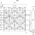
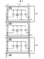
- FIG. 3 is a block diagram illustrating a schematic configuration of the liquid crystal display device 100. As shown in FIG. 3, the liquid crystal display device 100 includes a portion where a plurality of gate lines G1, G2, G3, G4 and a plurality of source lines S1, S2, S3, S4, S5, S6, S7, S8 intersect.
- a display unit 101 in which pixels (display pixels) 20 (A1 to A4, B1 to B4, C1 to C4, D1 to D4) including a switching element 21, a pixel electrode 22, and a pixel capacitor 23 are arranged correspondingly, and A source driver 102 for supplying source signals to the source lines S1, S2, S3, S4, S5, S6, S7, S8; a gate driver 103 for supplying gate signals to the gate lines G1, G2, G3, G4; And a CS driver 104 for supplying a CS voltage (Vsc) to the storage capacitor line CS connected to the pixel capacitor 23.
- Vsc CS voltage
- the liquid crystal display device 100 further includes a backlight, an optical film, and the like (not shown).
- the liquid crystal display device 100 includes a display control device 105 that performs display control of the liquid crystal display device 100. Details of the display control device 105 will be described later.
- the extending direction of the scanning signal lines is described as a row direction or a horizontal direction
- the extending direction of the data signal lines is described as a column direction or a vertical direction. Therefore, in the display unit 101 shown in FIG. 3, the first row is the pixels 20A1, 20A2, 20A3, 20A4, the second row is the pixels 20B1, 20B2, 20B3, 20B4, and the third row is the pixels 20C1, 20C2, 20C3. , 20C4, the fourth row is the pixel 20D1, 20D2, 20D3, 20D4.
- the first column of the display unit 101 is the pixels 20A1, 20B1, 20C1, 20D1
- the second column is the pixels 20A2, 20B2, 20C2, 20D2
- the third column is the pixels 20A3, 20B3, 20C3, 20D3, and 4 columns.
- the eyes are the pixels 20A4, 20B4, 20C4, 20D4.
- the liquid crystal display device 100 has a so-called double source structure, and two data signal lines are provided per pixel column. Specifically, in one pixel column, odd-numbered pixels are connected to one of these two source lines via a switching element, and even-numbered pixels have a switching element on the other of these two source lines. Connected through. That is, in the double source structure, since one pixel is sandwiched between two source lines and the upper and lower two lines are driven by the same gate line, the source signal is transmitted simultaneously for two lines, and the two lines are simultaneously transmitted. Switching is performed and display data is written.
- the pixel 20A1 is connected to the source line S1 via the switching element 21, and the pixel 20B1 is connected to the source line S2 via the switching element 21. Connected to.
- the pixel 20A2 adjacent to the pixel 20A1 in the row direction is connected to the source line S4 via the switching element 21, and is adjacent to the pixel 20B1 in the row direction.
- 20B2 is connected to the source line S3 via the switching element 21.
- the source lines S2 and S3 are adjacent.
- two-line simultaneous selection for selecting two adjacent gate lines is performed. For example, the simultaneous selection of the gate lines G1 and G2 and the simultaneous selection of the gate lines G3 and G4 are sequentially performed.
- the liquid crystal display device 100 includes a portion where a plurality of gate lines (G1, G2, G3, G4, etc And a plurality of source lines (S1, S2, S3, S4,%) Intersect.
- Display pixels (20A1, 20A2, 20A3, 20A4,...) Are arranged corresponding to each, and the display pixels (20A1, 20B1) are sandwiched between two source lines (S1, S2) and vertically
- Two display pixels (20A1, 20B1) are connected to different source lines (S1, S2), respectively, and the upper and lower display pixels (20A1, 20B1) are driven by the same gate line (G1, G2).
- Device is arranged corresponding to each, and the display pixels (20A1, 20B1) are sandwiched between two source lines (S1, S2) and vertically
- Two display pixels (20A1, 20B1) are connected to different source lines (S1, S2), respectively, and the upper and lower display pixels (20A1, 20B1) are driven by the same gate line (G1, G2).
- the liquid crystal display device 100 having the double source structure for example, when the number of scanning signal lines is 3240 or more and the diagonal is 60 inches or more, or when the refresh rate is 120 Hz, even if the source double-side input driving is performed, the single source structure
- the charging rate is insufficient, but the double source structure has an advantage that the charging rate can be increased.
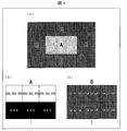
- FIG. 4A shows the input image data to be displayed on the display unit 101 of the liquid crystal display device 100
- FIG. 4B shows the area A (killer pattern) of the input image data shown in FIG.
- (C) shows a region B of the input image data shown in (a) of FIG.
- the input image data has 256 gradations.
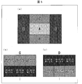
- FIG. 5A shows a display example when the input image data shown in FIG. 4A is actually displayed
- FIG. 5B shows a region C of the display example shown in FIG. (C) shows a region D shown in (a) of FIG.
- the region A (killer) is displayed as shown in FIG.
- the upper area C and the lower area D of the pattern) are brighter than the area B.
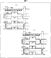
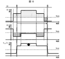
- the regions C and D are referred to as vertical shadow (transfer). The cause of the transfer will be described below with reference to FIGS.
- FIG. 6A shows a waveform diagram of the source voltage and liquid crystal voltage of one frame
- FIG. 6B shows a voltage applied to each pixel in the current frame corresponding to the waveform diagram shown in FIG.
- C is a diagram showing the polarity of the voltage applied to each pixel in the next frame corresponding to the waveform diagram shown in (a) of FIG.
- FIG. 7A shows a waveform diagram of the source voltage and the liquid crystal voltage in the next frame of the waveform diagram of FIG. 6A
- FIG. 7B corresponds to the waveform diagram shown in FIG.
- FIG. 7C shows the polarity of the voltage applied to each pixel in the current frame
- FIG. 7C shows the polarity of the voltage applied to each pixel in the next frame corresponding to the waveform diagram shown in FIG. .
- the voltages of the source lines S1 and S2 are equal when writing in the regions C and D, but the voltages in the region A are biased.
- the voltage fluctuation changes the voltage applied to the liquid crystal via the source lines S1 and S2 and the parasitic capacitance of the pixel.
- the plus pixel in the region C (the pixel to which the voltage is applied by the source line S1) is bright and the minus pixel (the pixel to which the voltage is applied by the source line S2). ) Becomes darker.
- the polarity is reversed in the next frame, so that the voltage deviation changes in the negative direction. Therefore, the plus pixel (pixel to which a voltage is applied by the source line S2) in the region D is dark, and the minus pixel (pixel to which a voltage is applied by the source line S1) is bright. This is the opposite of region C.
- the voltage value applied on the source lines at both ends of the pixel is integrated for one frame period, and the amount of transfer is suppressed by adjusting the correction amount according to the integrated value. Specifically, the occurrence of transfer is suppressed by a correction circuit described below.
- FIG. 1 is a schematic block diagram of the correction circuit 11 according to the present embodiment.
- the correction circuit 11 is provided in the display control device 105 provided in the liquid crystal display device 100.
- the correction circuit 11 integrates the voltage values corresponding to the input gradation applied from the source lines (S1, S2) to the display pixels (20A1, 20B1) on the same gate line (G1, G2) for one frame period.
- the voltage value obtained by adding the difference between the obtained integrated values to each of the voltage values corresponding to the input gradation is set as the output gradation of the current frame to be given to the two display pixels (20A1, 20B1). .
- the correction circuit 11 sets a voltage value corresponding to the input gradation of the previous frame applied from the source lines S1 and S2 to the display pixels (20A1 and 20B1) on the same gate line G1 and G2.
- Each of the two display pixels is integrated with a voltage value obtained by accumulating the difference between the obtained accumulated values for each one frame period and adding to the voltage value corresponding to the input gradation of the previous frame delayed by one frame period.
- the output gradation of the current frame given to (20A1, 20B1) is used.
- the configuration is as follows.
- the correction circuit 11 includes an input unit 1, a gradation voltage conversion unit 2, a vertical voltage integration unit (integration unit) 3, a coefficient multiplication unit (difference calculation unit) 4, a correction value calculation unit (difference calculation). Section) 5, a frame memory delay adjusting section 6, a correction value adding section (adding section) 7, and an output section 8.
- the input unit 1 receives image data of an image to be displayed on the liquid crystal display device 100 and outputs the image data to the subsequent gradation voltage conversion unit 2 and the frame memory delay adjustment unit 6.
- the gradation voltage conversion unit 2 converts the image data (input gradation) input from the input unit 1 into a voltage and outputs the voltage to the vertical voltage integration unit 3 at the subsequent stage.
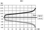
- the gradation voltage conversion unit 2 converts the input gradation to a voltage using, for example, an LUT (lookup table) as shown in FIG.
- LUT lookup table
- Vcom is used as a reference
- the voltage on the VL side is negative
- the voltage on the VH side is positive.
- the vertical voltage integration unit 3 integrates the voltage values on the source lines S1 and S2 on the same gate line for one frame period, that is, the period from the rising edge of the gate signal to the rising edge of the next gate signal, Is output to the coefficient multiplier 4.
- the source voltages of the source lines S1 and S2 shown in FIG. Here, in the regions C and D, the source voltage is 0 because the source voltage is equal, but the region A does not become 0 because the source voltage is biased.
- Coefficient multiplying unit 4 the integrated value [Delta] V Sou1 source lines S1 obtained from the vertical integrated voltage unit 3 multiplies the integrated value [Delta] V Sou2, coefficients in each of the source lines S2, the voltage fluctuation between the source lines S1, S2 A value (voltage shift amount ⁇ V (difference)) is calculated, and this voltage shift amount ⁇ V is output to the correction value calculation unit 5 at the subsequent stage.
- the voltage fluctuation value (voltage shift amount ⁇ V (difference)) of the pixel is obtained from the parasitic capacitances (C sou1 , C sou2 ).
- the voltage shift amount ⁇ V is calculated by the following equation (1).
- the correction value calculation unit 5 calculates a correction value (correction gradation) from the voltage shift amount ⁇ V from the coefficient multiplication unit 4 and the gradation of the display pixel and outputs the correction value (correction gradation) to the subsequent correction value addition unit 7. Specifically, the correction amount is obtained by the following equation (2).
- the frame memory delay adjusting unit 6 delays the input of the image data input to the input unit 1 to the correction value adding unit 7 by one frame. Thereby, the frame to be corrected and the frame for obtaining the correction value can be made the same, which is effective when the display image changes for each frame such as a moving image.
- the correction value addition unit 7 adds the correction value (correction gradation) of the correction value calculation unit 5 to the gradation of the display image delayed by one frame by the frame memory delay adjustment unit 6, thereby correcting the output gradation after correction. Is output to the output unit 8.
- the correction value calculated by the correction value calculation unit 5 is not only a positive number but also a negative number. For example, in the display image shown in FIG. 5A, a pixel that becomes bright has a negative correction value, and a pixel that becomes dark has a positive correction value.
- the output unit 8 sends the corrected output gradation from the correction value adding unit 7 to the source driver 102.
- the correction circuit 11 calculates the input gradation of the previous frame applied from the source line to the upper and lower two display pixels (20A1, 20B1) on the same gate line (G1, G2).
- a gradation voltage conversion unit 2 for converting to a voltage value
- a vertical voltage integration unit 3 for integrating the two voltage values converted by the gradation voltage conversion unit 2 for one frame period, and an integration by the vertical voltage integration unit 3
- the difference calculating unit (coefficient multiplying unit 4, correction value calculating unit 5) for obtaining the difference between the two integrated values obtained and the difference obtained by the difference calculating unit (coefficient multiplying unit 4, correction value calculating unit 5)
- a correction value adding unit 7 for adding to each voltage value corresponding to the input gradation of the previous frame stored in the frame memory, and the voltage values added by the correction value adding unit 7 are displayed in the two displays.
- FIG. 8 shows waveform diagrams of the source voltage and liquid crystal voltage of the source lines S1 and S2 before and after correction.
- the correction circuit 11 obtains a correction value for canceling the change in luminance from the integrated value obtained by integrating the source voltages of the source lines S1 and S2 before correction shown in FIG.
- the output gradation is determined by adding the value to the input data delayed by one frame.
- the source voltages (solid lines in the figure) of the corrected source lines S1 and S2 shown in (b) of FIG. 8 are obtained.
- the broken lines in the waveform diagram of FIG. 8B indicate the source voltage and liquid crystal voltage of the source lines S1 and S2 before correction.
- the killer pattern as shown in FIG. 4A is displayed by displaying the image with the output gradation corrected by the correction circuit 11, the occurrence of transfer in the displayed image is prevented. Can be suppressed. That is, it is possible to provide a liquid crystal display device with high display quality that does not generate transfer when a killer pattern display such as a 1-dot horizontal stripe is performed by the correction circuit 11 of the display control device 105 according to the present embodiment.
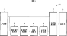
- FIG. 9 is a block diagram of a schematic configuration of the correction circuit 12 according to the present embodiment.
- the correction circuit 12 includes an input unit 1, a gradation voltage conversion unit 2, a vertical voltage integration unit 3, a coefficient multiplication unit 4, a correction value calculation unit 5, a correction value addition unit 7, and an output unit 8. Contains.
- the only difference from the correction circuit 11 described in the first embodiment is that the frame memory delay adjustment unit 6 is not included, and the other configurations are the same.
- the correction circuit 12 sets the voltage value corresponding to the input gradation of the previous frame applied from the source lines S1 and S2 to the display pixels (20A1 and 20B1) on the same gate line (G1 and G2) by 1 respectively. Accumulating the frame period, and adding the difference between the obtained integrated values to each of the voltage values corresponding to the input gradation of the current frame gives the current values to the two display pixels (20A1, 20B1).
- the output gradation of the frame Specifically, it is as follows.
- the correction circuit 12 is a gradation voltage for converting the input gradation of the previous frame applied from the source line to the two upper and lower display pixels (20A1, 20B1) on the same gate line (G1, G2) into a voltage value.
- the difference between the conversion unit 2, the vertical voltage integration unit 3 that integrates the two voltage values converted by the gradation voltage conversion unit 2 for one frame period, and the two integration values integrated by the vertical voltage integration unit 3 The coefficient multiplication unit 4 and the correction value calculation unit 5 for obtaining the difference, and the correction value addition for adding the difference obtained by the coefficient multiplication unit 4 and the correction value calculation unit 5 to each voltage value corresponding to the input gradation of the current frame And a voltage value added by the correction value adding unit 7 as an output gradation of the current frame to be given to the two display pixels (20A1, 20B1).
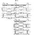
- the correction circuit 12 assuming that the display image shown in FIG. 4A is a still image will be described.
- FIG. 10 shows waveform diagrams of the source voltage and the liquid crystal voltage of the source lines S1 and S2 before and after correction. However, it differs from the case of FIG. 8 in that the source voltage of the current frame is corrected using a correction value obtained from the integrated value obtained by integrating the source voltage of the previous frame for one frame period.
- the data of the previous frame is the same image as the current frame.
- the absolute value is the same only by the sign of the integrated voltage value being reversed. Therefore, the correction value is obtained by calculating the correction amount using the reverse sign of the integrated value of the previous frame.
- the correction value calculation unit 5 obtains a correction value by calculating the correction amount using the reverse sign of the integrated value of the previous frame as described above, and the correction value addition unit 7
- the output gradation is obtained by adding the correction value obtained by the correction value calculation unit 5 to the display data of the frame.
- the correction circuit 12 does not require a frame delay, the frame memory and the frame memory delay adjustment unit 6 are not necessary.
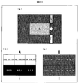
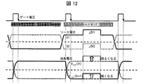
- FIG. 11 is a diagram showing a killer pattern. This killer pattern is the same killer pattern as in FIG. 4A, but differs in that it is scrolled horizontally.
- FIG. 12 shows waveform diagrams of the source voltage and liquid crystal voltage of the source lines S1 and S2 in the killer pattern shown in FIG.
- regions E and F shown in FIG. 11A are all regions B in the source line direction in the previous frame. Since the data of the current frame is different, correction cannot be performed correctly.
- the killer pattern display such as a 1-dot horizontal stripe
- the correction circuit 12 of the display control apparatus 105 a display in which no transfer occurs.
- a high-quality liquid crystal display device can be provided.
- a period in which voltage values corresponding to input gradations applied to the source lines (S1, S2) arranged on both sides of the display pixel (20A1) are integrated is described as one frame.
- the present invention is not limited to this, and the integration period may be 0.5 frames or more. That is, the period during which the voltage values are integrated may be any period that can reduce the influence on the display pixels. If the integration period is shorter than 0.5 frames, correction cannot be sufficiently performed with the obtained integration amount.
- the display pixels (20A1, 20A2, 20A3, 20A4,...) Are arranged corresponding to each of the portions, and the source lines (S1, S2) are arranged on both sides of the display pixel (20A1).
- the display control device 105 controls the display of the liquid crystal display device 100 having the structure, and the voltages correspond to the input gradations applied to the source lines (S1, S2) arranged on both sides of the display pixel (20A1).
- the value is integrated for a period of 0.5 frame or more, the difference between the two obtained integrated values is added to the voltage value corresponding to the input gradation, and the obtained voltage value is given to the display pixel.
- Frame It is characterized in that it includes a correction circuit to force the tone (11, 12).
- the display pixels are affected by the source lines arranged on both sides. Therefore, as in the above configuration, the voltage values corresponding to the input gradations applied to the source lines (S1, S2) arranged on both sides of the display pixel (20A1) are integrated over a period of 0.5 frames or more.
- the difference between the two obtained integrated values is a correction value that cancels the influence (change in luminance) of the source line that the display pixel receives.
- This correction value is added to the voltage value corresponding to the input gradation, and the obtained voltage value is used as the output gradation of the current frame given to the display pixel.
- voltage fluctuations applied to the display pixels are reduced, so that it is difficult for a deviation from the gradation to be displayed to occur.
- the display pixels sandwiched between the two source lines can suppress the occurrence of transfer (vertical shadow) due to the influence of the source lines, thereby improving the display quality.
- a plurality of gate lines (G1, G2, G3, G4,...) And a plurality of source lines (S1, S2, S3, S4,%) Intersect.
- Display pixels (20A1, 20A2, 20A3, 20A4,...) are arranged corresponding to the portions to be displayed, and the display pixels (20A1, 20B1) are sandwiched between two source lines (S1, S2).
- the upper and lower two display pixels (20A1, 20B1) are connected to different source lines (S1, S2), respectively, and the upper and lower two display pixels (20A1, 20B1) are driven by the same gate line (G1, G2).
- the display control device 105 of the liquid crystal display device 100 includes source pixels (S1, S2) connected to display pixels (20A1, 20B1) on the same gate line (G1, G2).
- the voltage values corresponding to the input gray scale applied from each are integrated by 0.5 frames or more (one frame period), and the difference between the obtained integrated values is added to the voltage value corresponding to the input gray scale.
- It includes a correction circuit (11, 12) for applying the obtained voltage value to the output gradation of the current frame to be applied to the two display pixels.
- the voltage values corresponding to the input gradations applied to the two display pixels on the same gate line are each integrated for one frame period, and the difference between the obtained integrated values is the difference between the two display pixels.
- the voltage value obtained by adding this difference to each voltage value corresponding to the input gradation is set as the output gradation of the current frame given to the two display pixels, so that the voltage applied to the two display pixels can be reduced. Since the fluctuation is reduced, it is difficult for the deviation from the gradation to be displayed to occur.
- the correction circuit (11) is applied to the source lines (S1, S2) disposed on both sides of the display pixels (20A1, 20B1), respectively.
- the period for accumulating voltage values corresponding to the input gradations is one frame, it is applied from the source lines (S1, S2) to the display pixels (20A1, 20B1) on the same gate line (G1, G2).
- Each voltage value corresponding to the input gradation of the previous frame is integrated for one frame period, and the difference between the obtained integrated values is added to each voltage value corresponding to the input gradation of the previous frame delayed by one frame period.
- the voltage value obtained in this way may be the output gradation of the current frame given to the two display pixels (20A1, 20B1).
- the output gradation of the current frame is obtained by adding the voltage fluctuation (difference of one frame period integrated value) due to the input gradation of the previous frame to the input gradation of the previous frame.
- the display image can be corrected correctly.
- correction can be performed correctly when the image changes from frame to frame, such as a moving image, display quality does not deteriorate due to the correction.
- a specific display control apparatus is as follows.
- the correction circuit (11) is configured so that the upper and lower display pixels (20A1, 20B1) on the same gate line (G1, G2) are connected to the source line.
- a gradation voltage conversion unit 2 that converts the input gradation of the previous frame applied to a voltage value
- an integration unit vertical that integrates the two voltage values converted by the gradation voltage conversion unit 2 for one frame period, respectively.
- the correction circuit (12) is applied to the source lines (S1, S2) arranged on both sides of the display pixels (20A1, 20B1), respectively.
- Each of the voltage values corresponding to the key is integrated for one frame period, and the difference between the obtained integrated values is added to each voltage value corresponding to the input gradation of the current frame.
- the output gradation of the current frame given to the pixels (20A1, 20B1) may be used.
- the output gradation of the current frame is obtained by adding the voltage fluctuation (difference of one frame period integrated value) due to the input gradation of the previous frame to the input gradation of the current frame. Therefore, it is not necessary to provide a frame memory for delaying the previous frame by one frame period.
- the display image can be corrected correctly by the above configuration.
- the correction circuit (12) is connected to the upper and lower display pixels (20A1, 20B1) on the same gate line (G1, G2) from the source line.
- a gradation voltage conversion unit 2 that converts the input gradation of the previous frame applied to a voltage value
- an integration unit vertical that integrates the two voltage values converted by the gradation voltage conversion unit 2 for one frame period, respectively.
- a voltage integrating unit 3 A voltage integrating unit 3
- a difference calculating unit coefficient multiplying unit 4, correction value calculating unit 5) for obtaining a difference between two integrated values integrated by the integrating unit (vertical voltage integrating unit 3), and the difference calculating unit
- An addition unit that adds the difference obtained by (coefficient multiplication unit 4 and correction value calculation unit 5) to each voltage value corresponding to the input gradation of the current frame.
- Part (correction value addition The voltage value added by section 7), preferably in the output gray level of the current frame to be supplied to the two display pixels (20A1,20B1).
- the liquid crystal display device according to aspect 7 of the present invention may include the display control device according to any one of aspects 1 to 6.
- the display quality of the liquid crystal display device can be improved.
- the display control apparatus may be realized by a computer.
- the display control apparatus is realized by a computer by operating the computer as a correction circuit included in the display control apparatus.
- a display control program of the display control device and a computer-readable recording medium on which the display control program is recorded also fall within the scope of the present invention.
- the present invention can be suitably used for a liquid crystal display device of a double source drive system.
Landscapes
- Physics & Mathematics (AREA)
- Engineering & Computer Science (AREA)
- General Physics & Mathematics (AREA)
- Theoretical Computer Science (AREA)
- Crystallography & Structural Chemistry (AREA)
- Chemical & Material Sciences (AREA)
- Computer Hardware Design (AREA)
- Nonlinear Science (AREA)
- Optics & Photonics (AREA)
- Mathematical Physics (AREA)
- Control Of Indicators Other Than Cathode Ray Tubes (AREA)
- Liquid Crystal Display Device Control (AREA)
- Liquid Crystal (AREA)
Abstract
Description
本発明の実施の形態について説明すれば以下の通りである。
図3は、液晶表示装置100の概略構成を示すブロック図である。液晶表示装置100は、図3に示すように、複数のゲートラインG1,G2,G3,G4と複数のソースラインS1,S2,S3,S4,S5,S6,S7,S8とが交差する部分のそれぞれに対応してスイッチング素子21、画素電極22及び画素容量23を含む画素(表示画素)20(A1~A4,B1~B4,C1~C4,D1~D4)が配置された表示部101と、上記ソースラインS1,S2,S3,S4,S5,S6,S7,S8にソース信号を供給するソースドライバ102と、上記ゲートラインG1,G2,G3,G4にゲート信号を供給するゲートドライバ103と、上記画素容量23に接続された保持容量配線CSにCS電圧(Vsc)を供給するCSドライバ104と、を含んでいる。
図4の(a)は、液晶表示装置100の表示部101に表示させる入力画像データを示し、(b)は、同図の(a)に示す入力画像データの領域A(キラーパターン)を示し、(c)は、同図の(a)に示す入力画像データの領域Bを示している。ここで、入力画像データは256階調とする。
図1は、本実施形態に係る補正回路11の概略構成ブロック図である。なお、補正回路11は、上記液晶表示装置100に備えられた表示制御装置105内に設けられている。
補正値算出部5は、係数乗算部4からの電圧シフト量ΔVと表示画素の階調から補正値(補正階調)を算出し、後段の補正値加算部7に出力する。補正量は、具体的には、以下の式(2)により求める。ここで、Din:入力階調、ΔV:電圧シフト量、ΔD:補正階調(補正値)、V(Din):階調=>電圧関数、invV(Din):電圧=>階調関数
ΔD=invV(V(Din)+ΔV)・・・・(2)
なお、実際のLSIでは、上記補正値算出部5における演算は回路規模が大きいため、2次元LUT F(Din,ΔV)を用いて演算を簡略化するのが好ましい。
図8は、補正前後のソースラインS1,S2のソース電圧及び液晶電圧の波形図を示している。
本発明の他の実施形態について説明すれば、以下のとおりである。なお、説明の便宜上、前記実施形態にて説明した部材と同じ機能を有する部材については、同じ符号を付記し、その説明を省略する。
図9は、本実施形態に係る補正回路12の概略構成ブロック図である。
図10は、補正前後のソースラインS1,S2のソース電圧及び液晶電圧の波形図を示している。但し、図8の場合とは、現フレームのソース電圧は、前フレームのソース電圧を1フレーム期間積算した積算値から得られた補正値を用いて補正する点で異なる。
ここで、図9に示す補正回路12によって、補正が正しく行えないキラーパターンについて説明する。
本発明の態様1に係る表示制御装置は、複数のゲートライン(G1,G2,G3,G4,・・・)と複数のソースライン(S1,S2,S3,S4,・・・)とが交差する部分のそれぞれに対応して表示画素(20A1,20A2,20A3,20A4,・・・)が配置されるとともに、上記表示画素(20A1)の両側に上記ソースライン(S1,S2)が配置された構造の液晶表示装置100の表示を制御する表示制御装置105であって、上記表示画素(20A1)の両側に配置されたソースライン(S1,S2)にそれぞれ印加される入力階調に対応する電圧値を、0.5フレーム以上の期間積算し、得られた2つの積算値の差分を、上記入力階調に対応する電圧値に加算し、得られた電圧値を、当該表示画素に与える現フレームの出力階調とする補正回路(11,12)を含んでいることを特徴としている。
2 階調電圧変換部
3 垂直電圧積算部(積算部)
4 係数乗算部(差分演算部)
5 補正値算出部(差分演算部)
6 フレームメモリ遅延調整部
7 補正値加算部(加算部)
8 出力部
11、12 補正回路
20 画素(表示画素)
20A1~20A4 画素(表示画素)
20B1~20B4 画素(表示画素)
20C1~20C4 画素(表示画素)
20D1~20D4 画素(表示画素)
21 スイッチング素子
22 画素電極
23 画素容量
100 液晶表示装置
101 表示部
102 ソースドライバ
103 ゲートドライバ
104 CSドライバ
105 表示制御装置
A~F 領域
CS 保持容量配線
G1~G4 ゲートライン
S1~S8 ソースライン
Claims (9)
- 複数のゲートラインと複数のソースラインとが交差する部分のそれぞれに対応して表示画素が配置されるとともに、上記表示画素の両側に上記ソースラインが配置された構造の液晶表示装置の表示を制御する表示制御装置であって、
上記表示画素の両側に配置されたソースラインにそれぞれ印加される入力階調に対応する電圧値を0.5フレーム以上の期間積算し、得られた2つの積算値の差分を、入力階調に対応する電圧値に加算し、得られた電圧値を、当該表示画素に与える現フレームの出力階調とする補正回路を含んでいることを特徴とする表示制御装置。 - 複数のゲートラインと複数のソースラインとが交差する部分のそれぞれに対応して表示画素が配置されるとともに、上記表示画素は2つのソースラインに挟まれ、且つ上下2つの表示画素がそれぞれ異なるソースラインに接続され、当該上下2つの表示画素が同一のゲートラインで駆動される液晶表示装置の表示を制御する表示制御装置であって、
上記同一のゲートライン上の上下2つの表示画素にソースラインからそれぞれ印加される入力階調に対応する電圧値をそれぞれ0.5フレーム以上の期間積算し、得られた2つの積算値の差分を、入力階調に対応する電圧値のそれぞれに加算して得られた電圧値を、上記2つの表示画素に与える現フレームのそれぞれの出力階調とする補正回路を含んでいることを特徴とする表示制御装置。 - 上記補正回路は、
上記表示画素の両側に配置されたソースラインにそれぞれ印加される入力階調に対応する電圧値を積算する期間が1フレームであるとき、
同一のゲートライン上の上下2つの表示画素にソースラインからそれぞれ印加される前フレームの入力階調に対応する電圧値をそれぞれ1フレーム期間積算し、得られた2つの積算値の差分を、1フレーム期間遅延させた前フレームの入力階調に対応する電圧値のそれぞれに加算して得られた電圧値を、上記2つの表示画素に与える現フレームのそれぞれの出力階調とすることを特徴とする請求項2に記載の表示制御装置。 - 上記補正回路は、
同一のゲートライン上の上下2つの表示画素にソースラインからそれぞれ印加される前フレームの入力階調を電圧値に変換する階調電圧変換部と、
上記階調電圧変換部によって変換された2つの電圧値をそれぞれ1フレーム期間積算する積算部と、
上記積算部によって積算された2つの積算値の差分を求める差分演算部と、
上記差分演算部によって求められた差分を、フレームメモリに格納された前フレームの入力階調に対応する電圧値のそれぞれに加算する加算部と、
を含み、上記加算部によって加算された電圧値を、上記2つの表示画素に与える現フレームのそれぞれの出力階調とすることを特徴とする請求項3に記載の表示制御装置。 - 上記補正回路は、
上記表示画素の両側に配置されたソースラインにそれぞれ印加される入力階調に対応する電圧値を積算する期間が1フレームであるとき、
同一のゲートライン上の表示画素に印加される前フレームの入力階調に対応する電圧値をそれぞれ1フレーム期間積算し、得られた積算値の差分を、現フレームの入力階調に対応する電圧値のそれぞれに加算して得られた電圧値を、上記2つの表示画素に与える現フレームの出力階調とすることを特徴とする請求項2に記載の表示制御装置。 - 上記補正回路は、
同一のゲートライン上の上下2つの表示画素にソースラインからそれぞれ印加される前フレームの入力階調を電圧値に変換する階調電圧変換部と、
上記階調電圧変換部によって変換された2つの電圧値をそれぞれ1フレーム期間積算する積算部と、
上記積算部によって積算された2つの積算値の差分を求める差分演算部と、
上記差分演算部によって求められた差分を、現フレームの入力階調に対応する電圧値のそれぞれに加算する加算部と、
を含み、上記加算部によって加算された電圧値を、上記2つの表示画素に与える現フレームの出力階調とすることを特徴とする請求項5に記載の表示制御装置。 - 請求項1~6の何れか1項に記載の表示制御装置を備えた液晶表示装置。
- 請求項1~6の何れか1項に記載の表示制御装置としてコンピュータを機能させるための表示制御プログラムであって、上記補正回路としてコンピュータを機能させるための表示制御プログラム。
- 請求8に記載の表示制御プログラムを記録したコンピュータ読み取り可能な記録媒体。
Priority Applications (4)
| Application Number | Priority Date | Filing Date | Title |
|---|---|---|---|
| US15/567,618 US20180122311A1 (en) | 2015-04-24 | 2016-04-14 | Display control device, liquid crystal display apparatus, and storage medium |
| EP16783090.0A EP3288019A1 (en) | 2015-04-24 | 2016-04-14 | Display control device, liquid crystal display device, display control program, and recording medium |
| CN201680023893.9A CN107533830A (zh) | 2015-04-24 | 2016-04-14 | 显示控制装置、液晶显示装置、显示控制程序和记录介质 |
| JP2017514091A JP6526801B2 (ja) | 2015-04-24 | 2016-04-14 | 表示制御装置、液晶表示装置、表示制御プログラム及び記録媒体 |
Applications Claiming Priority (2)
| Application Number | Priority Date | Filing Date | Title |
|---|---|---|---|
| JP2015-089827 | 2015-04-24 | ||
| JP2015089827 | 2015-04-24 |
Publications (1)
| Publication Number | Publication Date |
|---|---|
| WO2016171069A1 true WO2016171069A1 (ja) | 2016-10-27 |
Family
ID=57144441
Family Applications (1)
| Application Number | Title | Priority Date | Filing Date |
|---|---|---|---|
| PCT/JP2016/062023 Ceased WO2016171069A1 (ja) | 2015-04-24 | 2016-04-14 | 表示制御装置、液晶表示装置、表示制御プログラム及び記録媒体 |
Country Status (5)
| Country | Link |
|---|---|
| US (1) | US20180122311A1 (ja) |
| EP (1) | EP3288019A1 (ja) |
| JP (1) | JP6526801B2 (ja) |
| CN (1) | CN107533830A (ja) |
| WO (1) | WO2016171069A1 (ja) |
Cited By (2)
| Publication number | Priority date | Publication date | Assignee | Title |
|---|---|---|---|---|
| WO2018154728A1 (ja) * | 2017-02-24 | 2018-08-30 | 堺ディスプレイプロダクト株式会社 | 表示装置 |
| WO2019083016A1 (ja) * | 2017-10-27 | 2019-05-02 | シャープ株式会社 | 表示制御装置、液晶表示装置およびテレビジョン受像機 |
Families Citing this family (1)
| Publication number | Priority date | Publication date | Assignee | Title |
|---|---|---|---|---|
| CN109979404B (zh) * | 2019-03-07 | 2020-10-13 | 深圳市华星光电半导体显示技术有限公司 | 显示面板充电方法以及装置 |
Citations (4)
| Publication number | Priority date | Publication date | Assignee | Title |
|---|---|---|---|---|
| WO2010079641A1 (ja) * | 2009-01-09 | 2010-07-15 | シャープ株式会社 | カラー表示装置 |
| WO2012111553A1 (ja) * | 2011-02-18 | 2012-08-23 | シャープ株式会社 | 表示装置の駆動方法、プログラム、および表示装置 |
| JP2013134400A (ja) * | 2011-12-27 | 2013-07-08 | Seiko Epson Corp | 画像処理装置、プロジェクターおよび画像処理方法 |
| JP2014178362A (ja) * | 2013-03-13 | 2014-09-25 | Seiko Epson Corp | 表示制御回路、電気光学装置、及び、電子機器 |
Family Cites Families (4)
| Publication number | Priority date | Publication date | Assignee | Title |
|---|---|---|---|---|
| TW518882B (en) * | 2000-03-27 | 2003-01-21 | Hitachi Ltd | Liquid crystal display device for displaying video data |
| KR101710611B1 (ko) * | 2010-07-30 | 2017-02-28 | 삼성디스플레이 주식회사 | 표시 패널의 구동 방법 및 이를 수행하는 표시 장치 |
| KR20160055620A (ko) * | 2014-11-10 | 2016-05-18 | 삼성디스플레이 주식회사 | 표시 패널의 구동 방법 및 이를 수행하는 표시 장치 |
| KR20160083325A (ko) * | 2014-12-30 | 2016-07-12 | 삼성디스플레이 주식회사 | 표시 장치 및 그 데이터 처리 방법 |
-
2016
- 2016-04-14 CN CN201680023893.9A patent/CN107533830A/zh active Pending
- 2016-04-14 EP EP16783090.0A patent/EP3288019A1/en not_active Withdrawn
- 2016-04-14 US US15/567,618 patent/US20180122311A1/en not_active Abandoned
- 2016-04-14 WO PCT/JP2016/062023 patent/WO2016171069A1/ja not_active Ceased
- 2016-04-14 JP JP2017514091A patent/JP6526801B2/ja not_active Expired - Fee Related
Patent Citations (4)
| Publication number | Priority date | Publication date | Assignee | Title |
|---|---|---|---|---|
| WO2010079641A1 (ja) * | 2009-01-09 | 2010-07-15 | シャープ株式会社 | カラー表示装置 |
| WO2012111553A1 (ja) * | 2011-02-18 | 2012-08-23 | シャープ株式会社 | 表示装置の駆動方法、プログラム、および表示装置 |
| JP2013134400A (ja) * | 2011-12-27 | 2013-07-08 | Seiko Epson Corp | 画像処理装置、プロジェクターおよび画像処理方法 |
| JP2014178362A (ja) * | 2013-03-13 | 2014-09-25 | Seiko Epson Corp | 表示制御回路、電気光学装置、及び、電子機器 |
Non-Patent Citations (1)
| Title |
|---|
| See also references of EP3288019A4 * |
Cited By (8)
| Publication number | Priority date | Publication date | Assignee | Title |
|---|---|---|---|---|
| WO2018154728A1 (ja) * | 2017-02-24 | 2018-08-30 | 堺ディスプレイプロダクト株式会社 | 表示装置 |
| CN110291574A (zh) * | 2017-02-24 | 2019-09-27 | 堺显示器制品株式会社 | 显示装置 |
| US10964278B2 (en) | 2017-02-24 | 2021-03-30 | Sakai Display Products Corporation | Display apparatus |
| CN110291574B (zh) * | 2017-02-24 | 2022-07-12 | 堺显示器制品株式会社 | 显示装置 |
| WO2019083016A1 (ja) * | 2017-10-27 | 2019-05-02 | シャープ株式会社 | 表示制御装置、液晶表示装置およびテレビジョン受像機 |
| CN111279409A (zh) * | 2017-10-27 | 2020-06-12 | 夏普株式会社 | 显示控制装置、液晶显示装置及电视接收机 |
| US10997934B2 (en) | 2017-10-27 | 2021-05-04 | Sharp Kabushiki Kaisha | Display control device, liquid crystal display device, and television receiver |
| CN111279409B (zh) * | 2017-10-27 | 2022-05-10 | 夏普株式会社 | 显示控制装置、液晶显示装置及电视接收机 |
Also Published As
| Publication number | Publication date |
|---|---|
| JPWO2016171069A1 (ja) | 2017-12-07 |
| US20180122311A1 (en) | 2018-05-03 |
| CN107533830A (zh) | 2018-01-02 |
| JP6526801B2 (ja) | 2019-06-05 |
| EP3288019A4 (en) | 2018-02-28 |
| EP3288019A1 (en) | 2018-02-28 |
Similar Documents
| Publication | Publication Date | Title |
|---|---|---|
| JP6682491B2 (ja) | 表示制御装置、液晶表示装置およびテレビジョン受像機 | |
| JP4197322B2 (ja) | 表示装置,液晶モニター,液晶テレビジョン受像機および表示方法 | |
| JP5373587B2 (ja) | 液晶表示装置とその駆動方法 | |
| US9704428B2 (en) | Display device and display method | |
| JP5049101B2 (ja) | 液晶表示装置 | |
| US9299318B2 (en) | Display device and image signal compensating method | |
| WO2010073775A1 (ja) | 表示装置および表示装置の駆動方法 | |
| JPWO2010087051A1 (ja) | 表示装置および表示装置の駆動方法 | |
| KR20120005813A (ko) | 표시 패널의 구동 방법 및 이를 수행하기 위한 표시 장치 | |
| JP5154655B2 (ja) | 表示装置および表示装置の駆動方法ならびに表示駆動の制御方法 | |
| US20080150865A1 (en) | Lcd and drive method thereof | |
| KR20150047965A (ko) | 액정 표시 장치 및 그 구동 방법 | |
| JP5522334B2 (ja) | 液晶駆動方法及び液晶駆動装置 | |
| JP6526801B2 (ja) | 表示制御装置、液晶表示装置、表示制御プログラム及び記録媒体 | |
| WO2009133906A1 (ja) | 映像信号線駆動回路および液晶表示装置 | |
| JP2007225861A (ja) | 液晶表示装置 | |
| WO2011074285A1 (ja) | 液晶表示装置および液晶表示装置の駆動方法 | |
| KR20120089081A (ko) | 액정 표시 장치, 영상 신호 보정 장치 및 영상 신호 보정 방법 | |
| TWI485692B (zh) | 源極驅動裝置及顯示面板的驅動方法 | |
| JP4910499B2 (ja) | 表示ドライバ、電気光学装置、電子機器及び駆動方法 | |
| WO2013015209A1 (ja) | 液晶表示装置 | |
| JP2011197353A (ja) | 表示装置、および表示装置の駆動方法 | |
| KR20060134779A (ko) | 액정 표시 장치 및 그의 구동 방법 | |
| JP4893726B2 (ja) | 表示装置及びその駆動方法 | |
| JP2009271267A (ja) | 駆動装置、表示装置及びその駆動方法 |
Legal Events
| Date | Code | Title | Description |
|---|---|---|---|
| 121 | Ep: the epo has been informed by wipo that ep was designated in this application |
Ref document number: 16783090 Country of ref document: EP Kind code of ref document: A1 |
|
| ENP | Entry into the national phase |
Ref document number: 2017514091 Country of ref document: JP Kind code of ref document: A |
|
| REEP | Request for entry into the european phase |
Ref document number: 2016783090 Country of ref document: EP |
|
| WWE | Wipo information: entry into national phase |
Ref document number: 15567618 Country of ref document: US |
|
| NENP | Non-entry into the national phase |
Ref country code: DE |