WO2016157307A1 - Step-up device and converter device - Google Patents
Step-up device and converter device Download PDFInfo
- Publication number
- WO2016157307A1 WO2016157307A1 PCT/JP2015/059681 JP2015059681W WO2016157307A1 WO 2016157307 A1 WO2016157307 A1 WO 2016157307A1 JP 2015059681 W JP2015059681 W JP 2015059681W WO 2016157307 A1 WO2016157307 A1 WO 2016157307A1
- Authority
- WO
- WIPO (PCT)
- Prior art keywords
- control unit
- booster
- shunt
- shunt resistor
- current
- Prior art date
Links
Images


Classifications
-
- H—ELECTRICITY
- H02—GENERATION; CONVERSION OR DISTRIBUTION OF ELECTRIC POWER
- H02M—APPARATUS FOR CONVERSION BETWEEN AC AND AC, BETWEEN AC AND DC, OR BETWEEN DC AND DC, AND FOR USE WITH MAINS OR SIMILAR POWER SUPPLY SYSTEMS; CONVERSION OF DC OR AC INPUT POWER INTO SURGE OUTPUT POWER; CONTROL OR REGULATION THEREOF
- H02M3/00—Conversion of dc power input into dc power output
- H02M3/02—Conversion of dc power input into dc power output without intermediate conversion into ac
- H02M3/04—Conversion of dc power input into dc power output without intermediate conversion into ac by static converters
- H02M3/10—Conversion of dc power input into dc power output without intermediate conversion into ac by static converters using discharge tubes with control electrode or semiconductor devices with control electrode
- H02M3/145—Conversion of dc power input into dc power output without intermediate conversion into ac by static converters using discharge tubes with control electrode or semiconductor devices with control electrode using devices of a triode or transistor type requiring continuous application of a control signal
- H02M3/155—Conversion of dc power input into dc power output without intermediate conversion into ac by static converters using discharge tubes with control electrode or semiconductor devices with control electrode using devices of a triode or transistor type requiring continuous application of a control signal using semiconductor devices only
- H02M3/156—Conversion of dc power input into dc power output without intermediate conversion into ac by static converters using discharge tubes with control electrode or semiconductor devices with control electrode using devices of a triode or transistor type requiring continuous application of a control signal using semiconductor devices only with automatic control of output voltage or current, e.g. switching regulators
- H02M3/158—Conversion of dc power input into dc power output without intermediate conversion into ac by static converters using discharge tubes with control electrode or semiconductor devices with control electrode using devices of a triode or transistor type requiring continuous application of a control signal using semiconductor devices only with automatic control of output voltage or current, e.g. switching regulators including plural semiconductor devices as final control devices for a single load
- H02M3/1584—Conversion of dc power input into dc power output without intermediate conversion into ac by static converters using discharge tubes with control electrode or semiconductor devices with control electrode using devices of a triode or transistor type requiring continuous application of a control signal using semiconductor devices only with automatic control of output voltage or current, e.g. switching regulators including plural semiconductor devices as final control devices for a single load with a plurality of power processing stages connected in parallel
-
- H—ELECTRICITY
- H02—GENERATION; CONVERSION OR DISTRIBUTION OF ELECTRIC POWER
- H02M—APPARATUS FOR CONVERSION BETWEEN AC AND AC, BETWEEN AC AND DC, OR BETWEEN DC AND DC, AND FOR USE WITH MAINS OR SIMILAR POWER SUPPLY SYSTEMS; CONVERSION OF DC OR AC INPUT POWER INTO SURGE OUTPUT POWER; CONTROL OR REGULATION THEREOF
- H02M1/00—Details of apparatus for conversion
- H02M1/0003—Details of control, feedback or regulation circuits
- H02M1/0009—Devices or circuits for detecting current in a converter
-
- H—ELECTRICITY
- H02—GENERATION; CONVERSION OR DISTRIBUTION OF ELECTRIC POWER
- H02M—APPARATUS FOR CONVERSION BETWEEN AC AND AC, BETWEEN AC AND DC, OR BETWEEN DC AND DC, AND FOR USE WITH MAINS OR SIMILAR POWER SUPPLY SYSTEMS; CONVERSION OF DC OR AC INPUT POWER INTO SURGE OUTPUT POWER; CONTROL OR REGULATION THEREOF
- H02M1/00—Details of apparatus for conversion
- H02M1/0003—Details of control, feedback or regulation circuits
- H02M1/0025—Arrangements for modifying reference values, feedback values or error values in the control loop of a converter
-
- H—ELECTRICITY
- H02—GENERATION; CONVERSION OR DISTRIBUTION OF ELECTRIC POWER
- H02M—APPARATUS FOR CONVERSION BETWEEN AC AND AC, BETWEEN AC AND DC, OR BETWEEN DC AND DC, AND FOR USE WITH MAINS OR SIMILAR POWER SUPPLY SYSTEMS; CONVERSION OF DC OR AC INPUT POWER INTO SURGE OUTPUT POWER; CONTROL OR REGULATION THEREOF
- H02M3/00—Conversion of dc power input into dc power output
- H02M3/02—Conversion of dc power input into dc power output without intermediate conversion into ac
- H02M3/04—Conversion of dc power input into dc power output without intermediate conversion into ac by static converters
- H02M3/10—Conversion of dc power input into dc power output without intermediate conversion into ac by static converters using discharge tubes with control electrode or semiconductor devices with control electrode
- H02M3/145—Conversion of dc power input into dc power output without intermediate conversion into ac by static converters using discharge tubes with control electrode or semiconductor devices with control electrode using devices of a triode or transistor type requiring continuous application of a control signal
- H02M3/155—Conversion of dc power input into dc power output without intermediate conversion into ac by static converters using discharge tubes with control electrode or semiconductor devices with control electrode using devices of a triode or transistor type requiring continuous application of a control signal using semiconductor devices only
- H02M3/156—Conversion of dc power input into dc power output without intermediate conversion into ac by static converters using discharge tubes with control electrode or semiconductor devices with control electrode using devices of a triode or transistor type requiring continuous application of a control signal using semiconductor devices only with automatic control of output voltage or current, e.g. switching regulators
- H02M3/158—Conversion of dc power input into dc power output without intermediate conversion into ac by static converters using discharge tubes with control electrode or semiconductor devices with control electrode using devices of a triode or transistor type requiring continuous application of a control signal using semiconductor devices only with automatic control of output voltage or current, e.g. switching regulators including plural semiconductor devices as final control devices for a single load
- H02M3/1584—Conversion of dc power input into dc power output without intermediate conversion into ac by static converters using discharge tubes with control electrode or semiconductor devices with control electrode using devices of a triode or transistor type requiring continuous application of a control signal using semiconductor devices only with automatic control of output voltage or current, e.g. switching regulators including plural semiconductor devices as final control devices for a single load with a plurality of power processing stages connected in parallel
- H02M3/1586—Conversion of dc power input into dc power output without intermediate conversion into ac by static converters using discharge tubes with control electrode or semiconductor devices with control electrode using devices of a triode or transistor type requiring continuous application of a control signal using semiconductor devices only with automatic control of output voltage or current, e.g. switching regulators including plural semiconductor devices as final control devices for a single load with a plurality of power processing stages connected in parallel switched with a phase shift, i.e. interleaved
Definitions
- the present invention relates to a booster device and a converter device that boost a DC voltage.
- the boost converter circuit includes a rectifier circuit that converts AC power into DC power, a coil and a switching element, a booster circuit that boosts a DC voltage output from the rectifier circuit, and a pulse width modulation (Pulse Width Modulation) And a control circuit that performs PWM) control.
- Patent Document 1 describes a digital converter 1 in which three boost choppers 4a to 4c are connected in parallel.
- the step-up choppers 4a to 4c are configured such that coils L1 to L3, switching elements Q1 to Q3, and shunt resistors R1 to R3 are connected in series.
- the one-chip microcomputer 3 sets the pulse width of the PWM wave based on the current Ipi at the time of OFF transition of each switching element (paragraphs 0013 and 0021 and FIG. 1).
- a plurality of switching elements can be operated under optimum conditions in accordance with the respective characteristics (paragraph 0017).
- the boost choppers 4a to 4c have shunt resistors R1 to R3, respectively. Therefore, since the digital converter 1 described in Patent Document 1 has a large number of parts, the cost and the mounting area are increased.
- the present invention has been made in view of the above, and an object of the present invention is to obtain a booster device capable of suppressing cost and mounting area.
- the present invention provides a shunt resistor having one end connected to the common bus on the low potential side and the other end of the shunt resistor and a high potential connected to each other in parallel. And a plurality of booster circuits connected to the input bus on the side.
- the booster according to the present invention has an effect that the cost and the mounting area can be suppressed.
- FIG. 1 is a flowchart showing the operation of the power supply device according to the first embodiment.
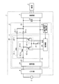
- FIG. 1 is a diagram illustrating a configuration of the power supply device according to the first embodiment.
- the power supply device 1 converts AC power supplied from the AC power source 2 into DC power, further converts DC power into AC power, and drives the load 3.
- the load 3 is exemplified by an electric motor.
- the power supply device 1 includes an input unit 4 to which AC power is input from the AC power source 2, a conversion unit 5 that converts AC power that has passed through the input unit 4 into DC power, and a DC voltage that is output from the conversion unit 5. And a conversion unit 7 that converts the DC power smoothed by the electrolytic capacitor 6 into AC power having a desired voltage and frequency and supplies the AC power to the load 3.
- the input unit 4 is exemplified by a noise filter.
- the input unit 4 filters noise of AC power input from the AC power supply 2.
- the conversion unit 7 is exemplified by a three-phase inverter device.
- the conversion unit 5 includes a converter device 11 that converts AC power that has passed through the input unit 4 into DC power, an anode connected to the converter device 11, and a cathode connected to the output bus 53 on the high potential side. 11 to 12-m (m is an integer of 2 or more), and a low potential side common bus 51 and a high potential side output bus 53. And a DC voltage detector 13 for detecting a voltage between them.
- the converter device 11 includes a rectifier 21 that converts AC power that has passed through the input unit 4 into DC power, a booster 22 that boosts a DC voltage output from the rectifier 21, and a controller 23 that controls the booster 22. And including.
- the rectifying unit 21 is exemplified by a diode bridge.
- the rectifier 21 performs full-wave rectification on the AC power that has passed through the input unit 4 and outputs DC power.
- the control unit 23 is exemplified by a CPU (Central Processing Unit) or a microcomputer. A voltage value between the common bus 51 and the output bus 53 is input to the control unit 23 from the DC voltage detection unit 13.
- CPU Central Processing Unit
- microcomputer A voltage value between the common bus 51 and the output bus 53 is input to the control unit 23 from the DC voltage detection unit 13.
- the boosting device 22 has a shunt resistor 31 having one end connected to the common bus 51 and a booster connected in parallel to each other between the other end of the shunt resistor 31 and the input bus 52 on the high potential side.
- Circuits 32-1 to 32-m (where m is an integer of 2 or more).
- the shunt resistor 31 is a resistor for detecting a current flowing from the booster circuit 32-1 to 32-m.
- the control unit 23 can calculate the current flowing through the shunt resistor 31 based on the voltage between both terminals of the shunt resistor 31.
- the current flowing through the shunt resistor 31 is referred to as a shunt current.
- the booster circuit 32-1 has a coil 41-1 which is an inductive element having one end connected to the input bus 52, and an input / output path connected between the other end of the coil 41-1 and the other end of the shunt resistor 31.
- Switching element 42-1 That is, the coil 41-1 and the switching element 42-1 are connected in series.
- the control terminal of the switching element 42-1 is connected to the control unit 23, and the switching element 42-1 is PWM-controlled by the control unit 23.
- the DC voltage boosted by the booster circuit 32-1 is output from the connection point between the coil 41-1 and the switching element 42-1.
- the anode of the diode 12-1 is connected to the connection point between the coil 41-1 and the switching element 42-1.
- the booster circuit 32-m has a coil 41-m, which is an inductive element having one end connected to the input bus 52, and an input / output path connected between the other end of the coil 41-m and the other end of the shunt resistor 31.
- Switching element 42-m That is, the coil 41-m and the switching element 42-m are connected in series.
- the control terminal of the switching element 42-m is connected to the control unit 23, and the switching element 42-m is PWM-controlled by the control unit 23.
- the DC voltage boosted by the booster circuit 32-m is output from the connection point between the coil 41-m and the switching element 42-m.
- the anode of the diode 12-m is connected to the connection point between the coil 41-m and the switching element 42-m.
- the coils 41-1 to 41-m preferably have a core with a small harmonic iron loss.
- the coils 41-1 to 41-m can be selected in consideration of the control method, efficiency, heat, mass, or volume.
- IGBTs Insulated Gate Bipolar Transistors
- MOSFETs Metal-Oxide-Semiconductor Field-Effect Transistors
- the control unit 23 controls the switching elements 42-1 to 42-m to turn on in order. That is, the switching elements 42-1 to 42-m are not simultaneously turned on.
- the control unit 23 does not perform switching from the switching elements 42-1 to 42-m.
- a voltage value between the common bus 51 and the output bus 53 is input to the control unit 23 from the DC voltage detection unit 13.
- the control unit 23 compares the voltage between the common bus 51 and the output bus 53 with a predetermined target voltage. When the voltage between the common bus 51 and the output bus 53 is higher than the target voltage, the control unit 23 short-circuits the switching elements 42-1 to 42-m.
- the control unit 23 stops switching from the switching elements 42-1 to 42-m.
- control unit 23 also stops switching from the switching elements 42-1 to 42-m even when the voltage between the common bus 51 and the output bus 53 is equal to the target voltage.
- the current flowing through the booster circuits 32-1 to 32-m is changed depending on the electrical characteristics or circuit patterns of the coils 41-1 to 41-m and the switching elements 42-1 to 42-m. Variations may occur.
- the control unit 23 performs PWM control of switching from the switching elements 42-1 to 42-m. Therefore, the control unit 23 determines that the current flowing through the shunt resistor 31 is from the booster circuits 32-1 to 32-m based on the timing of the ON period of the PWM signal applied to the switching elements 42-1 to 42-m. It is possible to determine which of the booster circuits is flowing.
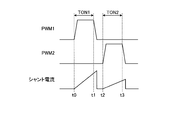
- FIG. 2 is a diagram illustrating an example of signal waveforms of the power supply device according to the first embodiment.
- the PWM signal applied to switching element 42-1 is referred to as signal PWM1
- the PWM signal applied to switching element 42-m is referred to as signal PWM2.
- the shunt current that is, the current flowing through the booster circuit 32-1, starts to rise.
- the shunt current that is, the current flowing through the booster circuit 32-1, begins to fall.
- the shunt current that is, the current flowing through the booster circuit 32-m starts to rise.
- the shunt current that is, the current flowing through the booster circuit 32-m starts to fall.
- time TON1 from timing t0 to t1 and the time TON2 from timing t2 to t3 are the same.
- the voltage is boosted by the electrical characteristics or circuit patterns from the coils 41-1 to 41-m and the switching elements 42-1 to 42-m. There may be variations in the current flowing through the circuits 32-1 to 32-m.
- the current flowing through the booster circuit 32-1 is larger than the current flowing through the booster circuit 32-m.
- the control unit 23 compares the shunt currents detected at different timings, that is, the currents flowing through the booster circuits 32-1 to 32-m. When the current flowing through the booster circuits 32-1 to 32-m varies, the control unit 23 switches the booster circuit with a small current among the booster circuits 32-1 to 32-m.
- the pulse widths of a plurality of PWM signals are corrected so that the on-time of the elements is increased and the on-time of the switching elements of the booster circuit having a large current in the booster circuits 32-1 to 32-m is shortened.
- the control unit 23 controls switching from the switching elements 42-1 to 42-m by using the corrected PWM signals.
- FIG. 3 is a flowchart of the operation of the power supply device according to the first embodiment.
- the flowchart shown in FIG. 3 shows the operation of the power supply device 1 for suppressing variation in the current flowing through the booster circuits 32-1 to 32-m.
- step S100 the control unit 23 collates the on-time timings of the plurality of PWM signals applied to the switching elements 42-1 to 42-m with the shunt current timings. Thereby, the control unit 23 determines which booster circuit among the booster circuits 32-1 to 32-m is the shunt current at each timing.
- step S102 the control unit 23 calculates a shunt current value that flows when a plurality of PWM signals applied to the switching elements 42-1 to 42-m are on. Specifically, the control unit 23 calculates the shunt current at the time of rising and the shunt current at the time of falling of the plurality of PWM signals applied to the switching elements 42-1 to 42-m. Then, the control unit 23 calculates the amount of increase in the shunt current during the on-time of each PWM signal by subtracting the shunt current at the rise of each PWM signal from the shunt current at the fall of each PWM signal.
- control unit 23 calculates the amount of increase in the shunt current during the on-time of each PWM signal, thereby removing the offset component and calculating the shunt current during the on-time of each PWM signal with high accuracy. can do.
- control unit 23 calculates the shunt current value IU1 when the signal PWM1 rises and the shunt current value ID1 when the signal PWM1 falls. Then, the control unit 23 calculates the increase ID1-IU1 of the shunt current during the on-time of the signal PWM1 by subtracting the shunt current IU1 at the rise of the signal PWM1 from the shunt current ID1 at the fall of the signal PWM1. .
- control unit 23 calculates the shunt current value IU2 when the signal PWM2 rises and the shunt current value ID2 when the signal PWM2 falls. Then, the control unit 23 calculates the increase ID2-IU2 of the shunt current during the ON time of the signal PWM2 by subtracting the shunt current IU2 at the rise of the signal PWM2 from the shunt current ID2 at the fall of the signal PWM2. .
- step S104 Based on the ratio of a predetermined shunt current target value to a shunt current value that flows when a plurality of PWM signals applied to the switching elements 42-1 to 42-m are on in step S104. Thus, a plurality of correction values for correcting the plurality of PWM signals are calculated.
- control unit 23 calculates a correction value M1 that is a ratio of the target value IS of the shunt current to the calculated shunt current value ID1-IU1 by using the equation (1).
- M1 IS / (ID1-IU1) (1)
- control unit 23 calculates a correction value M2 that is a ratio of the target value IS of the shunt current to the calculated shunt current value ID2-IU2 by the equation (2).
- M2 IS / (ID2-IU2) (2)
- step S106 the control unit 23 corrects the plurality of PWM signals by multiplying the ON times of the plurality of PWM signals applied to the switching elements 42-1 to 42-m by a plurality of correction values.
- control unit 23 corrects the ON time of the signal PWM1 to TON1 ⁇ M1 by multiplying the ON time TON1 of the signal PWM1 by the correction value M1.
- control unit 23 corrects the on-time of the signal PWM2 to TON2 ⁇ M2 by multiplying the on-time TON2 of the signal PWM2 by the correction value M2.
- FIG. 4 is a diagram illustrating an example of signal waveforms of the power supply device according to the first embodiment. As shown in FIG. 4, when the signal PWM1 begins to rise at timing t10, the shunt current, that is, the current flowing through the booster circuit 32-1, begins to rise.
- the shunt current that is, the current flowing through the booster circuit 32-1, starts to fall.
- the control unit 23 corrects the time TON1 to make the current value of the current flowing through the booster circuit 32-1 closer to the target current value.
- the control unit 23 calculates the shunt current value IU1 when the signal PWM1 rises and the shunt current value ID1 when the signal PWM1 falls. Then, the control unit 23 calculates the increase amount 72 of the shunt current during the ON time of the signal PWM1 by subtracting the shunt current IU1 at the rise of the signal PWM1 from the shunt current ID1 at the fall of the signal PWM1.
- the control unit 23 corrects the plurality of PWM signals based on a ratio of a predetermined target value of the shunt current to a shunt current value that flows when the plurality of PWM signals applied to the switching element 42-1 are on. A plurality of correction values are calculated.
- control unit 23 calculates a correction value M1 that is a ratio of the target value 73 of the shunt current to the calculated shunt current value 72 by the above-described equation (1).
- the control unit 23 corrects the ON time TON1 of the signal PWM1 to the ON time TON1A by multiplying the ON value TON1 of the signal PWM1 applied to the switching element 42-1 by the correction value M1.
- the shunt current that is, the current flowing through the booster circuit 32-1, starts to rise.
- the shunt current that is, the current flowing through the booster circuit 32-1, starts to fall.
- control unit 23 corrects the ON time TON1A of the signal PWM1 to be shorter than the ON time TON1 before correction. Therefore, the control unit 23 can control the current value 74 of the current flowing through the booster circuit 32-1 so as to approach the target current value.
- the power supply device 1 has the booster circuits 32-1 to 32-m according to the electrical characteristics or circuit patterns of the coils 41-1 to 41-m and the switching elements 42-1 to 42-m. Even if there is a variation in the current flowing through the current, the value of the current flowing through the booster circuits 32-1 through 32-m is corrected by correcting the PWM signal applied to the switching elements 42-1 through 42-m. It can be close to the target current value.
- the power supply device 1 can bring the current flowing from the booster circuits 32-1 to 32-m close to the target current value, it is possible to suppress the current from being concentrated on some elements. It is possible to suppress the generation of heat or power loss.
- the power supply device 1 includes one shunt resistor 31 between the common bus 51 and the booster circuits 32-1 to 32-m. Therefore, the power supply device 1 can reduce the number of parts, and can suppress the cost and the mounting area.
- the configuration described in the above embodiment shows an example of the contents of the present invention, and can be combined with another known technique, and can be combined with other configurations without departing from the gist of the present invention. It is also possible to omit or change the part.
- 1 power supply device 4 input unit, 5, 7 conversion unit, 6 electrolytic capacitor, 11 converter device, 12-1 to 12-m diode, 13 DC voltage detection unit, 21 rectification unit, 22 boosting device, 23 control unit, 31 Shunt resistor, 32-1 to 32-m booster circuit, 41-1 to 41-m coil, 42-1 to 42-m switching element.
Abstract
Description
図1は、実施の形態1にかかる電源装置の構成を示す図である。電源装置1は、交流電源2から供給される交流電力を直流電力に変換し、更に直流電力を交流電力に変換して、負荷3を駆動する。負荷3は、電動機が例示される。
FIG. 1 is a diagram illustrating a configuration of the power supply device according to the first embodiment. The
M1=IS/(ID1-IU1) ・・・(1) Specifically, the
M1 = IS / (ID1-IU1) (1)
M2=IS/(ID2-IU2) ・・・(2) Similarly, the
M2 = IS / (ID2-IU2) (2)
Claims (2)
- 一端が低電位側の共通母線に接続された1つのシャント抵抗と、
互いに並列接続されて、前記シャント抵抗の他端と高電位側の入力母線との間に接続された複数の昇圧回路と、
を備えることを特徴とする昇圧装置。 One shunt resistor with one end connected to the common bus on the low potential side;
A plurality of booster circuits connected in parallel to each other and connected between the other end of the shunt resistor and an input bus on the high potential side;
A booster device comprising: - 請求項1に記載の昇圧装置と、
前記複数の昇圧回路をパルス幅変調制御する制御部と、
を備え、
前記昇圧回路は、
一端が高電位側の入力母線に接続されたコイルと、入出力経路が前記コイルの他端と前記シャント抵抗の他端との間に接続され、制御端子に前記制御部からパルス幅変調信号が印加されるスイッチング素子と、を含み、
前記制御部は、
前記スイッチング素子に印加するパルス幅変調信号のオン時間のタイミングと、前記シャント抵抗を流れる電流のタイミングと、を照合することにより、前記シャント抵抗を流れる電流が前記複数の昇圧回路の中のどの昇圧回路を流れる電流であるかを判定し、前記スイッチング素子に印加するパルス幅変調信号がオンのときに流れるシャント抵抗を流れる電流値に対する、予め定められた目標電流値の比に基づいて、パルス幅変調信号を補正する
ことを特徴とするコンバータ装置。 A booster device according to claim 1;
A controller that performs pulse width modulation control on the plurality of booster circuits;
With
The booster circuit includes:
A coil having one end connected to the input bus on the high potential side, and an input / output path connected between the other end of the coil and the other end of the shunt resistor, and a pulse width modulation signal from the control unit to the control terminal An applied switching element,
The controller is
By comparing the timing of the on-time of the pulse width modulation signal applied to the switching element and the timing of the current flowing through the shunt resistor, the current flowing through the shunt resistor is boosted in any of the plurality of booster circuits. A pulse width based on a ratio of a predetermined target current value to a current value flowing through a shunt resistor flowing when a pulse width modulation signal applied to the switching element is on. A converter device for correcting a modulation signal.
Priority Applications (6)
| Application Number | Priority Date | Filing Date | Title |
|---|---|---|---|
| PCT/JP2015/059681 WO2016157307A1 (en) | 2015-03-27 | 2015-03-27 | Step-up device and converter device |
| CN201580075936.3A CN107210673B (en) | 2015-03-27 | 2015-03-27 | Converter apparatus |
| US15/538,069 US10084383B2 (en) | 2015-03-27 | 2015-03-27 | Booster device and converter device |
| EP15864316.3A EP3098955B1 (en) | 2015-03-27 | 2015-03-27 | Step-up device and converter device |
| JP2017508840A JP6479160B2 (en) | 2015-03-27 | 2015-03-27 | Converter device |
| AU2015389306A AU2015389306B2 (en) | 2015-03-27 | 2015-03-27 | Step-up device and converter device |
Applications Claiming Priority (1)
| Application Number | Priority Date | Filing Date | Title |
|---|---|---|---|
| PCT/JP2015/059681 WO2016157307A1 (en) | 2015-03-27 | 2015-03-27 | Step-up device and converter device |
Publications (1)
| Publication Number | Publication Date |
|---|---|
| WO2016157307A1 true WO2016157307A1 (en) | 2016-10-06 |
Family
ID=57005847
Family Applications (1)
| Application Number | Title | Priority Date | Filing Date |
|---|---|---|---|
| PCT/JP2015/059681 WO2016157307A1 (en) | 2015-03-27 | 2015-03-27 | Step-up device and converter device |
Country Status (6)
| Country | Link |
|---|---|
| US (1) | US10084383B2 (en) |
| EP (1) | EP3098955B1 (en) |
| JP (1) | JP6479160B2 (en) |
| CN (1) | CN107210673B (en) |
| AU (1) | AU2015389306B2 (en) |
| WO (1) | WO2016157307A1 (en) |
Cited By (2)
| Publication number | Priority date | Publication date | Assignee | Title |
|---|---|---|---|---|
| KR20190066288A (en) * | 2017-12-05 | 2019-06-13 | 엘지전자 주식회사 | Motor driving device and air conditioner including the same |
| JPWO2019171515A1 (en) * | 2018-03-07 | 2020-08-06 | 三菱電機株式会社 | Converter device |
Families Citing this family (7)
| Publication number | Priority date | Publication date | Assignee | Title |
|---|---|---|---|---|
| JP6950575B2 (en) * | 2018-02-26 | 2021-10-13 | トヨタ自動車株式会社 | Boost converter |
| US11268580B2 (en) * | 2018-06-13 | 2022-03-08 | Ka Group Ag | Electrically driven clutch actuator |
| CN111257728A (en) * | 2020-01-20 | 2020-06-09 | 广州华凌制冷设备有限公司 | Fault detection method, device, circuit and storage medium for boost voltage doubling circuit |
| CN111398782B (en) * | 2020-03-25 | 2021-11-26 | 美的集团股份有限公司 | Power supply circuit, circuit fault detection method, circuit board and vehicle-mounted air conditioner |
| CN111404373B (en) * | 2020-03-25 | 2021-06-18 | 广州华凌制冷设备有限公司 | Voltage doubling circuit, fault detection method, air conditioner and readable storage medium |
| CN111391612A (en) * | 2020-03-25 | 2020-07-10 | 广州华凌制冷设备有限公司 | Voltage doubling circuit, fault detection method, air conditioner and readable storage medium |
| CN111391609A (en) * | 2020-03-25 | 2020-07-10 | 广州华凌制冷设备有限公司 | Fault detection method and device for voltage doubling circuit, air conditioner and readable storage medium |
Citations (4)
| Publication number | Priority date | Publication date | Assignee | Title |
|---|---|---|---|---|
| JP2004297984A (en) * | 2003-03-28 | 2004-10-21 | Toyota Industries Corp | Driver of electromagnetic load |
| JP2006025579A (en) * | 2004-07-09 | 2006-01-26 | Sanyo Electric Co Ltd | Power circuit |
| JP2009261079A (en) | 2008-04-15 | 2009-11-05 | Diamond Electric Mfg Co Ltd | Digital converter and method of controlling the same |
| US20130194848A1 (en) * | 2012-01-31 | 2013-08-01 | Gabriele Bernardinis | Current-balancing in interleaved circuit phases |
Family Cites Families (23)
| Publication number | Priority date | Publication date | Assignee | Title |
|---|---|---|---|---|
| US5861734A (en) * | 1997-10-14 | 1999-01-19 | Lucent Technologies, Inc. | Control architecture for interleaved converters |
| EP0951133A3 (en) * | 1998-04-15 | 2000-04-12 | HILTI Aktiengesellschaft | Method and active filter for reducing ripple of a current drawn by a charge from a network |
| JP2002010632A (en) * | 2000-06-16 | 2002-01-11 | Origin Electric Co Ltd | Ac/dc converter and dc-dc converter |
| TW200507431A (en) * | 2003-08-11 | 2005-02-16 | Delta Electronics Inc | Current-balancing method and device for controlling the power-factor-correction circuit interlacedly |
| US7279868B2 (en) * | 2004-03-12 | 2007-10-09 | Comarco Wireless Technologies, Inc. | Power factor correction circuits |
| JP4784240B2 (en) | 2005-09-30 | 2011-10-05 | コニカミノルタオプト株式会社 | Manufacturing method of optical film |
| JP2007124831A (en) * | 2005-10-28 | 2007-05-17 | Nsk Ltd | Switching power supply circuit, on-vehicle switching power source device, electric power steering device and electric brake device therewith |
| JP2008105406A (en) | 2006-09-28 | 2008-05-08 | Brother Ind Ltd | Image formation apparatus |
| JP2008259307A (en) | 2007-04-04 | 2008-10-23 | Mitsubishi Electric Corp | Dc/dc converter and discharge lamp lighting apparatus using the dc/dc converter |
| US7884588B2 (en) * | 2008-04-10 | 2011-02-08 | Stmicroelectronics S.R.L. | Control method and device for a system of interleaved converters using a designated master converter |
| JP2009296851A (en) * | 2008-06-09 | 2009-12-17 | Sanken Electric Co Ltd | Power supply unit and method of controlling the same |
| ES2709773T3 (en) * | 2008-09-01 | 2019-04-17 | Mitsubishi Electric Corp | Circuit converter and control device for motor drive, air conditioner, refrigerator and cooker for induction heating equipped with circuit |
| JP2010233439A (en) * | 2009-03-03 | 2010-10-14 | Toshiba Corp | Power supply control device, and power supply apparatus using the same |
| WO2011122172A1 (en) * | 2010-03-29 | 2011-10-06 | ダイキン工業株式会社 | Switching power source circuit |
| JP5510048B2 (en) * | 2010-05-13 | 2014-06-04 | 株式会社豊田自動織機 | Power circuit |
| JP5635304B2 (en) * | 2010-05-25 | 2014-12-03 | セミコンダクター・コンポーネンツ・インダストリーズ・リミテッド・ライアビリティ・カンパニー | Power circuit |
| JP5604407B2 (en) | 2010-12-21 | 2014-10-08 | ローム アンド ハース カンパニー | Adhesive composition |
| JP5642047B2 (en) | 2010-12-21 | 2014-12-17 | ローム アンド ハース カンパニーRohm And Haas Company | Adhesive composition |
| JP6161866B2 (en) | 2010-12-21 | 2017-07-12 | ローム アンド ハース カンパニーRohm And Haas Company | Adhesive composition |
| WO2012137258A1 (en) * | 2011-04-08 | 2012-10-11 | 三菱電機株式会社 | Power conversion apparatus, motor drive apparatus, and refrigeration air-conditioning apparatus |
| JP2014054096A (en) | 2012-09-07 | 2014-03-20 | Toshiba Corp | Inverter device of air conditioner |
| US9240712B2 (en) * | 2012-12-13 | 2016-01-19 | Power Systems Technologies Ltd. | Controller including a common current-sense device for power switches of a power converter |
| CN104135002B (en) * | 2014-07-11 | 2017-06-06 | 邯郸美的制冷设备有限公司 | Alternating expression power factor corrector |
-
2015
- 2015-03-27 JP JP2017508840A patent/JP6479160B2/en active Active
- 2015-03-27 AU AU2015389306A patent/AU2015389306B2/en active Active
- 2015-03-27 US US15/538,069 patent/US10084383B2/en active Active
- 2015-03-27 EP EP15864316.3A patent/EP3098955B1/en active Active
- 2015-03-27 WO PCT/JP2015/059681 patent/WO2016157307A1/en active Application Filing
- 2015-03-27 CN CN201580075936.3A patent/CN107210673B/en active Active
Patent Citations (4)
| Publication number | Priority date | Publication date | Assignee | Title |
|---|---|---|---|---|
| JP2004297984A (en) * | 2003-03-28 | 2004-10-21 | Toyota Industries Corp | Driver of electromagnetic load |
| JP2006025579A (en) * | 2004-07-09 | 2006-01-26 | Sanyo Electric Co Ltd | Power circuit |
| JP2009261079A (en) | 2008-04-15 | 2009-11-05 | Diamond Electric Mfg Co Ltd | Digital converter and method of controlling the same |
| US20130194848A1 (en) * | 2012-01-31 | 2013-08-01 | Gabriele Bernardinis | Current-balancing in interleaved circuit phases |
Non-Patent Citations (1)
| Title |
|---|
| See also references of EP3098955A4 * |
Cited By (3)
| Publication number | Priority date | Publication date | Assignee | Title |
|---|---|---|---|---|
| KR20190066288A (en) * | 2017-12-05 | 2019-06-13 | 엘지전자 주식회사 | Motor driving device and air conditioner including the same |
| KR102080516B1 (en) * | 2017-12-05 | 2020-02-24 | 엘지전자 주식회사 | Motor driving device and air conditioner including the same |
| JPWO2019171515A1 (en) * | 2018-03-07 | 2020-08-06 | 三菱電機株式会社 | Converter device |
Also Published As
| Publication number | Publication date |
|---|---|
| JP6479160B2 (en) | 2019-03-06 |
| EP3098955A4 (en) | 2017-03-29 |
| CN107210673A (en) | 2017-09-26 |
| AU2015389306A1 (en) | 2017-07-13 |
| CN107210673B (en) | 2019-10-18 |
| EP3098955B1 (en) | 2018-10-10 |
| US20170353109A1 (en) | 2017-12-07 |
| US10084383B2 (en) | 2018-09-25 |
| AU2015389306B2 (en) | 2018-04-26 |
| JPWO2016157307A1 (en) | 2017-08-10 |
| EP3098955A1 (en) | 2016-11-30 |
Similar Documents
| Publication | Publication Date | Title |
|---|---|---|
| JP6479160B2 (en) | Converter device | |
| JP5182375B2 (en) | PFC converter | |
| JP5701283B2 (en) | Charger | |
| US10476395B2 (en) | Voltage converting system and method of using the same | |
| JP2013538544A (en) | AC / DC power conversion method and apparatus | |
| US9621046B2 (en) | Power converter for driving a switch based on current command and current flowing therein | |
| US10404171B2 (en) | Power converter circuit with a switched mode power converter that is switched based upon a measured inductor current and dynamically-determined first and second thresholds | |
| JP6535539B2 (en) | Power converter | |
| JPWO2015056571A1 (en) | Power conversion device and power conversion method | |
| US9130474B2 (en) | Power transforming apparatus with digital control unit | |
| JP2017028873A (en) | Power conversion device | |
| JP2008125313A (en) | Switching power supply | |
| US10432128B2 (en) | Frequency converter | |
| JP2008172979A (en) | Switching power supply device | |
| US20230299665A1 (en) | Power converting device | |
| JP5351944B2 (en) | Power converter | |
| JP5348427B2 (en) | Voltage converter and voltage control circuit | |
| JP6943110B2 (en) | Power converter | |
| CN110299823B (en) | Apparatus and method for controlling power supply | |
| JP6522227B2 (en) | Converter circuit, inverter circuit and power converter for air conditioner | |
| JP2016201194A (en) | LED lighting device | |
| JP2007143352A (en) | Power source voltage detection device of inverter | |
| US11258353B2 (en) | Power converter | |
| CN109075716B (en) | Clock-controlled power supply unit with galvanic isolation | |
| JP2022030037A (en) | Switching power supply device |
Legal Events
| Date | Code | Title | Description |
|---|---|---|---|
| REEP | Request for entry into the european phase |
Ref document number: 2015864316 Country of ref document: EP |
|
| WWE | Wipo information: entry into national phase |
Ref document number: 2015864316 Country of ref document: EP |
|
| 121 | Ep: the epo has been informed by wipo that ep was designated in this application |
Ref document number: 15864316 Country of ref document: EP Kind code of ref document: A1 |
|
| ENP | Entry into the national phase |
Ref document number: 2017508840 Country of ref document: JP Kind code of ref document: A |
|
| WWE | Wipo information: entry into national phase |
Ref document number: 15538069 Country of ref document: US |
|
| ENP | Entry into the national phase |
Ref document number: 2015389306 Country of ref document: AU Date of ref document: 20150327 Kind code of ref document: A |
|
| NENP | Non-entry into the national phase |
Ref country code: DE |