WO2016151817A1 - 導電体の形成方法 - Google Patents
導電体の形成方法 Download PDFInfo
- Publication number
- WO2016151817A1 WO2016151817A1 PCT/JP2015/059235 JP2015059235W WO2016151817A1 WO 2016151817 A1 WO2016151817 A1 WO 2016151817A1 JP 2015059235 W JP2015059235 W JP 2015059235W WO 2016151817 A1 WO2016151817 A1 WO 2016151817A1
- Authority
- WO
- WIPO (PCT)
- Prior art keywords
- layer
- conductor
- forming
- electrode
- light emitting
- Prior art date
- Legal status (The legal status is an assumption and is not a legal conclusion. Google has not performed a legal analysis and makes no representation as to the accuracy of the status listed.)
- Ceased
Links
Images




Classifications
-
- H—ELECTRICITY
- H05—ELECTRIC TECHNIQUES NOT OTHERWISE PROVIDED FOR
- H05B—ELECTRIC HEATING; ELECTRIC LIGHT SOURCES NOT OTHERWISE PROVIDED FOR; CIRCUIT ARRANGEMENTS FOR ELECTRIC LIGHT SOURCES, IN GENERAL
- H05B33/00—Electroluminescent light sources
- H05B33/10—Apparatus or processes specially adapted to the manufacture of electroluminescent light sources
-
- H—ELECTRICITY
- H05—ELECTRIC TECHNIQUES NOT OTHERWISE PROVIDED FOR
- H05B—ELECTRIC HEATING; ELECTRIC LIGHT SOURCES NOT OTHERWISE PROVIDED FOR; CIRCUIT ARRANGEMENTS FOR ELECTRIC LIGHT SOURCES, IN GENERAL
- H05B33/00—Electroluminescent light sources
- H05B33/12—Light sources with substantially two-dimensional [2D] radiating surfaces
- H05B33/26—Light sources with substantially two-dimensional [2D] radiating surfaces characterised by the composition or arrangement of the conductive material used as an electrode
- H05B33/28—Light sources with substantially two-dimensional [2D] radiating surfaces characterised by the composition or arrangement of the conductive material used as an electrode of translucent electrodes
-
- H—ELECTRICITY
- H10—SEMICONDUCTOR DEVICES; ELECTRIC SOLID-STATE DEVICES NOT OTHERWISE PROVIDED FOR
- H10K—ORGANIC ELECTRIC SOLID-STATE DEVICES
- H10K50/00—Organic light-emitting devices
- H10K50/80—Constructional details
- H10K50/805—Electrodes
- H10K50/81—Anodes
- H10K50/814—Anodes combined with auxiliary electrodes, e.g. ITO layer combined with metal lines
Definitions
- the present invention relates to a method for forming a conductor.
- a transparent electrode using a translucent conductive material is formed. Since the translucent conductive material generally has high resistance, the resistance of the transparent electrode is high. For this reason, in order to reduce the resistance of the transparent electrode, an auxiliary electrode may be formed on the transparent electrode, as described in Patent Document 1, for example.
- the auxiliary electrode is formed on a transparent electrode and is covered with an insulating film.
- Patent Document 1 describes ink jet printing as one of the auxiliary electrode forming methods.
- An example of a problem to be solved by the present invention is to reduce the resistance of a conductor by increasing the conductor without increasing the width of the conductor.
- the invention according to claim 1 is a step of forming the first layer by an inkjet method; Forming a second layer on the first layer by an inkjet method; Forming a conductor by heating the first layer and the second layer; It is the formation method of the conductor which has this.
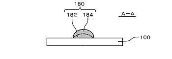
- FIG. 2 is a cross-sectional view taken along the line AA in FIG.
- FIG. 3 is a cross-sectional view taken along the line BB in FIG.
- It is a figure for demonstrating the formation method of a conductor. It is a figure which shows the result after investigating the time from forming a 1st layer to forming a 2nd layer, and the cross-sectional profile of a conductor. It is a top view which shows the structure of the conductor which concerns on 2nd Embodiment.
- FIG. 7 is a sectional view taken along line BB in FIG. 1 is a plan view illustrating a configuration of a light emitting device according to Example 1.
- FIG. 6 is a plan view illustrating a configuration of a light emitting device according to Example 2.
- FIG. 13 is a DD cross-sectional view of FIG. 12.
- 6 is a plan view showing a configuration of a light emitting device according to Example 3.
- FIG. 10 is a plan view showing a method for manufacturing the light emitting device according to Example 4;
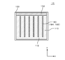
- FIG. 1 is a plan view of a conductor 180 according to the first embodiment.
- 2 is a cross-sectional view taken along the line AA in FIG. 1
- FIG. 3 is a cross-sectional view taken along the line BB in FIG.
- the conductor 180 according to the embodiment is formed on the substrate 100 and extends in the first direction (x direction in FIG. 1).
- the conductor 180 has a configuration in which the second layer 184 is overlaid on the first layer 182.
- Each of the first layer 182 and the second layer 184 has conductivity, and is formed by an ink jet method using ink containing conductive particles (for example, nano metal particles such as silver nanoparticles).
- the first layer 182 and the second layer 184 have a configuration in which a plurality of conductive particles are bonded by sintering.
- the heat treatment for sintering the plurality of conductive particles is performed after the first layer 182 and the second layer 184 are formed. For this reason, the boundary between the first layer 182 and the second layer 184 may not exist.
- the conductor 180 has two layers of a first layer 182 and a second layer 184.
- the conductor 180 is formed by repeatedly applying ink containing conductive particles.
- the conductor 180 can be made high without increasing the width of the conductor 180 (for example, 1.9). 2 times to 2.1 times).
- the width w of the conductor 180 is, for example, 100 ⁇ m or less, and the ratio of the height to the width of the conductor 180 (aspect ratio) is, for example, 0.002 (0.1 / 50) times or more.
- the conductor 180 may have a structure in which more layers are stacked (a structure in which multiple layers are applied). In this case, the conductor 180 can be further increased, and the above aspect ratio can be further increased.
- the first layer 182 and the second layer 184 of the conductor 180 are formed using an inkjet method. For this reason, as shown in FIGS. 2 and 3, the end portion of the conductor 180 is gradually thinned away from the center of the conductor 180.
- the conductor 180 is, for example, an auxiliary electrode of a transparent electrode of the light emitting device, but is not limited thereto. Further, another layer (for example, a transparent conductive layer) may be formed between the substrate 100 and the conductor 180.
- FIG. 4 is a diagram for explaining a method of forming the conductor 180.
- the process shown in this figure is performed in the atmosphere, for example.
- the substrate 100 is at room temperature (20 ° C.), for example.
- a first layer 182 is formed.
- the inkjet ejection head 200 has a plurality of ejection nozzles 202.
- droplets are ejected from some of the ejection nozzles 202 (for example, one ejection nozzle 202). It is preferable to discharge.
- the ejection head 200 is moved in the direction opposite to the first direction, and the ejection head 200 is returned to the predetermined position described above. Then, after a predetermined time has elapsed, ink droplets are ejected from the ejection nozzle 202 while moving the ejection head 200 in the first direction again. Thereby, the second layer 184 is formed on the first layer 182.
- the second layer 184 is formed after a predetermined time has elapsed since the first layer 182 was formed.
- the first layer 182 is dried to some extent before the second layer 184 is formed. Therefore, even if the second layer 184 is formed before the first layer 182 is sintered, the second layer 184 is stacked on the first layer 182.
- the height of the conductor 180 is increased by repainting the ink, and the conductor 180 does not spread during the repainting.
- corrugation of the surface of the 2nd layer 184 will become large too much.
- the degree of drying after ink is ejected from the ejection nozzle 202 until it adheres to the substrate 100 varies depending on the size of the droplet. For this reason, it is preferable to lengthen the said predetermined time as a droplet becomes large. Specifically, when the amount of droplets when forming the first layer 182 is a (picoliter: pl) and the predetermined time is b (seconds), 0.5 ⁇ b / a ⁇ 3 Preferably there is. If it does in this way, the dry state of the 1st layer 182 before the 2nd layer 184 is formed can be made into an appropriate state, for example, the state where the end of the 1st layer 182 was dried.
- the discharge nozzle 202 used when forming the second layer 184 is different from the discharge nozzle 202 used when forming the first layer 182, the first layer 182 and the second layer 184 are different. There is a high possibility that the position is shifted by several tens of ⁇ m in the y direction in FIG. This is because it is necessary to move the ejection head 200 in the y direction in FIG. 4 to perform alignment, and there is a limit to the accuracy of this alignment. Therefore, in the present embodiment, the same discharge nozzle 202 used when forming the first layer 182 is used as the discharge nozzle 202 used when forming the second layer 184. This eliminates the need to move the ejection head 200 in the y direction between the formation of the first layer 182 and the formation of the second layer 184. Therefore, the second layer 184 can be overlaid on the first layer 182 with high accuracy.
- the substrate 100 is heated.
- the plurality of conductive particles included in the first layer 182 and the plurality of conductive particles included in the second layer 184 are sintered to become the conductor 180.
- at least a part of the shape of the conductive particles remains in the conductor 180.
- the substrate 100 may be heated after forming the first layer 182 and before forming the second layer 184 in order to accelerate the drying of the first layer 182.
- the heating conditions (heating temperature and heating time) at this time are such that the conductive particles of the first layer 182 are not sintered. In this way, the formation time of the conductor 180 can be shortened.
- FIG. 5 shows the time (the above-mentioned predetermined time) from the formation of the first layer 182 to the formation of the second layer 184 in the case where the conductor 180 is formed using ink containing silver nanoparticles.
- FIG. 5 shows the result of having investigated the quality of the cross-sectional profile of the body 180.
- the conductor 180 is formed at atmospheric pressure, and the temperature of the substrate 100 is 20 ° C.
- the amount of liquid droplets discharged from the discharge nozzle 202 is 7 pl.
- b / a is 0.7 and 1.4
- the cross-sectional profile of the conductor 180 is good.
- b / a exceeds 5
- the cross-sectional profile of the conductor 180 deteriorates. From this, it can be said that 0.5 ⁇ b / a ⁇ 3 is preferable.
- the conductor 180 is formed by baking after applying ink repeatedly using the inkjet method. For this reason, the conductor 180 can be made high without increasing the width of the conductor 180. Therefore, the resistance of the conductor 180 can be reduced without increasing the width of the conductor 180.
- the second layer 184 of the conductor 180 is formed after the first layer 182 of the conductor 180 is dried to some extent, the width of the conductor 180 is not widened and the unevenness of the upper surface of the conductor 180 is small. .
- the width of the second layer 184 that is, the width of the conductor 180.
- the width of the conductor 180 does not increase.
- FIG. 6 is a plan view showing the configuration of the conductor 180 according to the second embodiment.
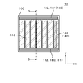
- 7 is a cross-sectional view taken along the line BB of FIG.
- the conductor 180 according to the present embodiment has the same configuration as that of the conductor 180 according to the first embodiment except that the conductor 180 includes the first portion 181 and the second portion 183.
- the first portion 181 is formed only by the first layer 182.
- the second portion 183 is formed by stacking the second layer 184 and the first layer 182. For this reason, the second portion 183 is thicker than the first portion 181. In order to do this, the second layer 184 may be formed only in a portion that becomes the second portion 183.
- the first portion 181 is formed by applying the conductive ink once, and the second portion 183 is formed by applying the conductive ink twice.
- the thickness of the second portion 183 is 180% or more and 220% or less of the thickness of the first portion 181.
- the second portion 183 may be further coated with conductive ink.
- the thickness of the second portion 183 is 90% to 110% of n times the thickness of the first portion 181 (where n is a positive number and 3 or more).
- the width of the first portion 181 is 90% or more and 120% or less of the width of the second portion 183.
- the length of the first portion 181 and the length of the first layer 182 are both 50 ⁇ m or more.
- the thickness of the first portion 181 and the thickness of the second portion 183 are both substantially constant except for the end portions. Further, at the boundary between the first portion 181 and the second portion 183, the thickness of the conductor 180 changes gently.
- the resistance of the conductor 180 can be lowered without increasing the width of the conductor 180.
- the width of the conductor 180 does not increase, and the unevenness of the upper surface of the conductor 180 is small. Then, only part of the conductor 180 can be thickened.
- FIG. 8 is a plan view illustrating the configuration of the light emitting device 10 according to the first embodiment.
- FIG. 9 is a diagram in which the second electrode 130 is removed from FIG.
- FIG. 10 is a diagram in which the insulating layer 150 and the organic layer 120 are removed from FIG.
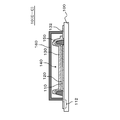
- FIG. 11 is a sectional view taken along the line CC of FIG.
- the sealing part 160 is abbreviate
- the light emitting device 10 includes a substrate 100, a light emitting unit 140, and a conductor 180.
- the light emitting unit 140 is formed on the substrate 100 and includes a first electrode 110, a second electrode 130, and an organic layer 120.
- the organic layer 120 is located between the first electrode 110 and the second electrode 130.
- the conductor 180 is an auxiliary electrode of the first electrode 110 and is in contact with any surface of the first electrode 110. In the example shown in this figure, the conductor 180 is formed on the surface of the first electrode 110 that faces the organic layer 120.
- the conductor 180 has the same configuration as that of the first embodiment.
- the light emitting device 10 will be described in detail.
- the substrate 100 is formed of a light-transmitting material such as glass or a light-transmitting resin.
- the substrate 100 may be formed of a material that does not have translucency.
- the substrate 100 is, for example, a polygon such as a rectangle.
- the substrate 100 may have flexibility.
- the thickness of the substrate 100 is, for example, not less than 10 ⁇ m and not more than 1000 ⁇ m.
- the thickness of the substrate 100 is, for example, 200 ⁇ m or less.
- the material of the substrate 100 includes, for example, PEN (polyethylene naphthalate), PES (polyethersulfone), PET (polyethylene terephthalate), or polyimide. Is formed.
- an inorganic barrier film such as SiN x or SiON is formed on at least the light emitting surface (preferably both surfaces) of the substrate 100 in order to suppress moisture from passing through the substrate 100. ing.
- a light emitting unit 140 is formed on the substrate 100.
- the light emitting unit 140 has a structure for generating light emission, for example, an organic EL element.
- This organic EL element has a configuration in which a first electrode 110, an organic layer 120, and a second electrode 130 are laminated in this order.
- the first electrode 110 is a transparent electrode having optical transparency.
- the transparent conductive material constituting the transparent electrode is a metal-containing material, for example, a metal oxide such as ITO (Indium Tin Oxide), IZO (Indium Zinc Oxide), IWZO (Indium Tungsten Zinc Oxide), ZnO (Zinc Oxide), and the like. is there.
- the thickness of the first electrode 110 is, for example, not less than 10 nm and not more than 500 nm.
- the first electrode 110 is formed using, for example, a sputtering method or a vapor deposition method.
- the first electrode 110 may be a carbon nanotube or a conductive organic material such as PEDOT / PSS.
- the second electrode 130 is made of, for example, a metal selected from the first group consisting of Al, Au, Ag, Pt, Mg, Sn, Zn, and In or an alloy of a metal selected from the first group. Contains a metal layer. In this case, the second electrode 130 has a light shielding property.
- the thickness of the second electrode 130 is, for example, not less than 10 nm and not more than 500 nm. However, the second electrode 130 may be formed using the material exemplified as the material of the first electrode 110.
- the second electrode 130 is formed using, for example, a sputtering method or a vapor deposition method.
- the materials of the first electrode 110 and the second electrode 130 described above are used when light is transmitted through the substrate 100, that is, when light emission from the light emitting device 10 is performed through the substrate 100 (that is, bottom emission type). It is an example. In other cases, light may pass through the side opposite to the substrate 100. That is, the light emission from the light emitting device 10 is performed without passing through the substrate 100 (top emission type).
- top emission type two types of laminated structures of a reverse product type and a forward product type can be adopted. In the reverse product type, the material of the first electrode 110 and the material of the second electrode 130 are opposite to those of the bottom emission type.
- the material of the second electrode 130 is used as the material of the first electrode 110, and the material of the first electrode 110 is used as the material of the second electrode 130.
- the material of the first electrode 110 is formed on the material of the second electrode 130 described above, the organic layer 120 is further formed thereon, and the second electrode 130 is further formed thinly thereon.
- the light is extracted from the side opposite to the substrate 100.
- the thin film forming material is, for example, the material exemplified as the material of the second electrode 130 or an MgAg alloy, and the thickness thereof is, for example, 30 nm or less.
- the light emitting device 10 according to the present embodiment may be of any structure of a bottom emission type and the two types of top emission types described above.
- the organic layer 120 has a configuration in which, for example, a hole injection layer, a light emitting layer, and an electron injection layer are stacked in this order.
- a hole transport layer may be formed between the hole injection layer and the light emitting layer.
- an electron transport layer may be formed between the light emitting layer and the electron injection layer.
- the organic layer 120 may be formed by a vapor deposition method.
- at least one layer of the organic layer 120, for example, a layer in contact with the first electrode may be formed by a coating method such as an inkjet method, a printing method, or a spray method. In this case, the remaining layers of the organic layer 120 are formed by vapor deposition.
- all the layers of the organic layer 120 may be formed using the apply
- the light emitting device 10 has a first terminal 112 and a second terminal 132.
- the first terminal 112 is connected to the first electrode 110
- the second terminal 132 is connected to the second electrode 130.
- the first terminal 112 and the second terminal 132 include a layer formed of the same material as that of the first electrode 110.
- a lead wiring may be provided between the first terminal 112 and the first electrode 110.
- a lead wiring may be provided between the second terminal 132 and the second electrode 130.
- a conductor 180 is formed on the first electrode 110.
- the conductor 180 is an auxiliary electrode for the first electrode 110, and a plurality of conductors 180 are formed on the first electrode 110.
- the conductors 180 extend in the y direction, and a plurality of conductors 180 are arranged at intervals in the x direction.
- the conductor 180 is formed using the method shown in the first embodiment. For this reason, the conductor 180 becomes high, and as a result, the cross-sectional area of the conductor 180 can be increased without increasing the width of the conductor 180. Therefore, the resistance of the conductor 180 can be reduced without expanding the region covered with the conductor 180 (that is, the region where light is not emitted) in the light emitting unit 140.
- the light emitting device 10 has an insulating layer 150.
- the insulating layer 150 is provided on the substrate 100 in order to define the light emitting region of the light emitting unit 140. In the example shown in FIG. 11, the insulating layer 150 covers the edge of the first electrode 110 and the conductor 180.
- the insulating layer 150 is made of, for example, polyimide, epoxy, acrylic, or novolac resin material.
- the insulating layer 150 is formed, for example, by mixing and applying a photosensitive material to a resin material to be the insulating layer 150, and then exposing and developing the resin material.
- the insulating layer 150 may be formed using an inkjet method or a screen printing method.
- the light emitting device 10 has a sealing portion 160.
- the sealing unit 160 seals the light emitting unit 140.
- the sealing portion 160 shown in this figure is a sealing member, and is formed using, for example, a metal such as glass or aluminum, or a resin.
- the sealing portion 160 is a polygon or a circle similar to the substrate 100, and has a shape in which a recess is provided at the center. The edge of the sealing portion 160 is fixed to the substrate 100 with an adhesive. Thereby, the space surrounded by the sealing portion 160 and the substrate 100 is sealed. And the light emission part 140 is located in this sealed space.
- the sealing member may be a film formed by an atomic layer deposition (ALD) method, a chemical vapor deposition (CVD) method, or a film formed by a sputtering method.
- the thickness of the sealing film is, for example, 10 nm or more and 1000 nm or less.
- the sealing film has, for example, at least one of an aluminum oxide film or a titanium oxide film.
- the sealing film is formed using a CVD method or a sputtering method, the sealing film is formed of an insulating film such as SiO 2 or SiN.
- the first electrode 110 is formed on the substrate 100.
- the first terminal 112 and the second terminal 132 are also formed.
- the conductor 180 is formed on the first electrode 110.
- the method for forming the conductor 180 is as described in the first embodiment.
- a resin material to be the insulating layer 150 is applied to the substrate 100, and this resin material is exposed and developed. Thereby, the insulating layer 150 is formed.
- the organic layer 120 is formed in a region surrounded by the first insulating layer 150 in the first electrode 110.
- the second electrode 130 is formed.
- the sealing part 160 is provided.
- the light emitting device 10 has the conductor 180 as the auxiliary electrode of the first electrode 110.
- the conductor 180 is formed by using the method shown in the first embodiment. For this reason, the conductor 180 becomes high. Therefore, the resistance of the conductor 180 can be reduced without expanding the region covered with the conductor 180 (that is, the region where light is not emitted) in the light emitting unit 140.
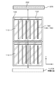
- FIG. 12 is a plan view illustrating a configuration of the light emitting device 10 according to the second embodiment, and corresponds to FIG. 10 in the first embodiment.
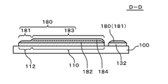
- 13 is a cross-sectional view taken along the line DD of FIG.
- the conductor 180 is also formed on the first terminal 112, and the conductor 180 is also formed on the second terminal 132.
- the configuration is the same as that of the light emitting device 10 according to the first embodiment.
- the conductor 180 on the first terminal 112 is formed continuously with the conductor 180 on the first electrode 110.
- the conductor 180 located on the 1st terminal 112 and the 1st electrode 110 has the structure shown in 2nd Embodiment.
- the conductor 180 on the first electrode 110 is the second portion 183
- the conductor 180 on the first terminal 112 is the first portion 181. Then, in the direction in which the second portion 183 extends, the second portion 183 and the first portion 181 are aligned and connected.
- the conductor 180 on the second terminal 132 is the first portion 181, it has the same thickness as the conductor 180 on the first terminal 112.
- the conductor 180 on the first terminal 112 and the conductor 180 on the second terminal 132 form the first portion 181 because the first terminal 112 and the second terminal 132 need to be translucent. This is because the resistance of the conductor 180 can be reduced by widening the width of the conductor 180.
- the width of the conductor 180 on the first terminal 112 may be the same as the width of the conductor 180 (that is, a portion functioning as an auxiliary electrode) (x direction in FIG. 12).
- the first terminal 112 is connected to a wiring for supplying current from the side surface side of the light emitting device 10. By doing so, the non-light emitting region can be reduced and the aperture ratio of the light emitting device 10 can be increased.
- first portion 181 of the conductor 180 may be provided in a portion that does not overlap with either the first terminal 112 or the second terminal 132.
- the manufacturing method of the light emitting device 10 according to the present embodiment is the same as the manufacturing method of the light emitting device 10 according to the first embodiment.
- the resistance of the conductor 180 can be reduced without expanding the region covered with the conductor 180 in the light emitting unit 140.
- the resistance of the first terminal 112 and the second terminal 132 can be reduced.
- the conductor 180 on the first terminal 112 and the conductor 180 on the second terminal 132 can be made thinner than the conductor 180 on the first electrode 110, The time for forming the conductor 180 on the second terminal 132 can be shortened.
- the first portion 181 is located in the light emitting region, and the second portion 183 is located in the non-light emitting region. In other words, the first portion 181 is on the first terminal 112.
- the second portion 183 is formed on the first electrode 110.
- the layout of the first portion 181 and the second portion 183 is not limited to this.
- the first portion 181 may be formed over the first electrode 110, and the second portion 183 may be formed only on a part of the first electrode 110, preferably near the center of the first electrode 110. This is for suppressing a decrease in luminance caused by an increase in resistance near the center of the light emitting surface of the light emitting device 10.
- the second portion 183 can be spot-formed at the place. Also in this case, since the thickness of the second portion 183 can be made an integral multiple of other portions, calculation of the current value / resistance value is relatively easy.
- FIG. 14 is a plan view illustrating a configuration of the light emitting device 10 according to the third embodiment, and corresponds to FIG. 12 in the second embodiment.
- the light emitting device 10 according to the present embodiment is related to the second embodiment except that the conductor 180 is formed under the first electrode 110, the first terminal 112, and the second terminal 132.
- the configuration is the same as that of the light emitting device 10.
- the conductor 180 is formed between the first electrode 110 and the substrate 100, between the first terminal 112 and the substrate 100, and between the second terminal 132 and the substrate 100, respectively. .
- the manufacturing method of the light emitting device 10 according to the present example is the light emission according to Example 2, except that the conductor 180 is formed before the first electrode 110, the first terminal 112, and the second terminal 132 are formed. This is the same as the manufacturing method of the device 10.
- the resistance of the conductor 180 can be reduced without expanding the region covered with the conductor 180 in the light emitting unit 140.
- the time for forming the conductor 180 on the first terminal 112 and the second terminal 132 can be shortened.
- FIG. 15 is a plan view illustrating the method for manufacturing the light emitting device 10 according to the fourth embodiment.
- the configuration of the light emitting device 10 is the same as that of any of the first to third embodiments.
- FIG. 15 shows the same case as in the first embodiment.
- the plurality of substrates 100 are connected to each other in the direction in which the conductor 180 extends (first direction: y direction in FIG. 15). Then, when forming the first layer 182 of the conductor 180, the ejection head 200 is moved in the first direction from the standby position. As a result, the first layer 182 of the conductor 180 is formed on each of the plurality of substrates 100.
- the ejection head 200 is moved in the direction opposite to the first direction (the direction of ⁇ y in FIG. 15) without ejecting ink, and returned to the standby position. During this return, the number of substrates 100 is set so that the predetermined time described in the first embodiment elapses.
- the second layer 184 is formed on each of the plurality of substrates 100 by moving the ejection head 200 again in the first direction.
- the plurality of substrates 100 are separated from each other. This separation may be performed after the sealing portion 160 is disposed (or formed) or may be performed before the light emitting device 10 is disposed (or formed).
- the first layer 182 is in a desired dry state while returning the ejection head 200 to the standby position in order to form the second layer 184. For this reason, it is not necessary to make the ejection head 200 stand by anywhere in order to dry the first layer 182. Therefore, the time required for manufacturing the light emitting device 10 is shortened.
- the some 1st electrode 110 is extended in the 1st direction
- the some 2nd electrode 130 is mentioned.
- a display device in which a plurality of light-emitting pixels are provided in a matrix by extending in a second direction orthogonal to the first direction and providing an organic layer at the intersection of the first electrode 110 and the second electrode 130,
- the present invention can be applied.
- a portion overlapping with the terminal may be the first portion 181
- a portion overlapping with the first electrode 110 may be the second portion 183.
- the present invention can employ various configurations other than those described above.
Landscapes
- Engineering & Computer Science (AREA)
- Manufacturing & Machinery (AREA)
- Electroluminescent Light Sources (AREA)
Abstract
第1層(182)をインクジェット法により形成する。次いで、第1層(182)の上に第2層(184)をインクジェット法により形成する。次いで、第1層(182)及び第2層(184)を加熱することにより、導電体(180)を形成する。第1層(182)と第2層(184)は、吐出ヘッド(200)の同一の吐出ノズル(202)を用いて形成されるのが好ましい。第2層(184)は、第1層(182)が形成された後、所定時間が経過してから形成される。
Description
本発明は、導電体の形成方法に関する。
基板に発光素子や光電変換素子などの光素子を形成した光装置には、透光性の導電材料を用いた透明電極が形成されている。透光性の導電材料は一般的に抵抗が高いため、透明電極の抵抗は高い。このため、透明電極の抵抗を下げるために、例えば特許文献1に記載されているように、透明電極には補助電極が形成されることがある。特許文献1において、補助電極は透明電極の上に形成されており、また、絶縁膜で被覆されている。また、特許文献1には、補助電極の形成方法の一つとして、インクジェット印刷が記載されている。
補助電極などの導電体の抵抗を下げるためには、導電体の断面積を広げる必要がある。導電体の断面積を広くするためには、導電体の幅を広くするか、導電体を高くする必要がある。しかし、導電体は一般的に遮光性の材料を用いて形成されているため、導電体の幅を広くすると、光素子のうち光が透過する領域が狭く、または、光装置の開口率が小さくなってしまう。また、インクジェット法による塗布により導電体を形成した場合に、導電体の高さを変更することは困難であった。
本発明が解決しようとする課題としては、導電体の幅を広げずに導電体を高くすることにより、導電体の抵抗を下げることが一例として挙げられる。
請求項1に記載の発明は、第1層をインクジェット法により形成する工程と、
前記第1層の上に、第2層をインクジェット法により形成する工程と、
前記第1層及び前記第2層を加熱することにより導電体を形成する工程と、
を有する導電体の形成方法である。
前記第1層の上に、第2層をインクジェット法により形成する工程と、
前記第1層及び前記第2層を加熱することにより導電体を形成する工程と、
を有する導電体の形成方法である。
上述した目的、およびその他の目的、特徴および利点は、以下に述べる好適な実施の形態、およびそれに付随する以下の図面によってさらに明らかになる。
以下、本発明の実施の形態について、図面を用いて説明する。尚、すべての図面において、同様な構成要素には同様の符号を付し、適宜説明を省略する。
(第1の実施形態)
図1は、第1の実施形態に係る導電体180の平面図である。図2は図1のA-A断面図であり、図3は図1のB-B断面図である。実施形態に係る導電体180は基板100の上に形成されており、第1の方向(図1におけるx方向)に延在している。導電体180は、第1層182の上に第2層184を重ねた構成を有している。第1層182及び第2層184は、いずれも導電性を有しており、導電粒子(例えば銀ナノ粒子などのナノ金属粒子)を含んだインクを用いて、インクジェット法により形成されている。このため、第1層182及び第2層184は、複数の導電粒子が焼結によって結合した構成を有している。なお、詳細を後述するように、複数の導電粒子を焼結するための熱処理は、第1層182及び第2層184が形成された後に行われている。このため、第1層182と第2層184の境界は存在しない場合もある。
図1は、第1の実施形態に係る導電体180の平面図である。図2は図1のA-A断面図であり、図3は図1のB-B断面図である。実施形態に係る導電体180は基板100の上に形成されており、第1の方向(図1におけるx方向)に延在している。導電体180は、第1層182の上に第2層184を重ねた構成を有している。第1層182及び第2層184は、いずれも導電性を有しており、導電粒子(例えば銀ナノ粒子などのナノ金属粒子)を含んだインクを用いて、インクジェット法により形成されている。このため、第1層182及び第2層184は、複数の導電粒子が焼結によって結合した構成を有している。なお、詳細を後述するように、複数の導電粒子を焼結するための熱処理は、第1層182及び第2層184が形成された後に行われている。このため、第1層182と第2層184の境界は存在しない場合もある。
また、図2及び図3に示す例において、導電体180は第1層182と第2層184の2層を有している。言い換えると、導電体180は導電粒子を含むインクを重ね塗りすることによって形成されている。このため、導電粒子を含むインクを重ね塗りせずに導電体180を形成した場合と比較して、導電体180の幅を広げずに、導電体180を高くすることができる(例えば1.9倍以上2.1倍以下)。また、導電体180の幅wは、例えば100μm以下であり、導電体180の幅に対する高さの比(アスペクト比)は、例えば0.002(0.1/50)倍以上になる。ただし、導電体180はさらに多くの層を重ねた構造(重ね塗りした構造)を有していてもよい。この場合、導電体180をさらに高くすることができ、また上記したアスペクト比をさらに大きくすることができる。
なお、上記したように、導電体180の第1層182及び第2層184はインクジェット法を用いて形成されている。このため、図2及び図3に示すように、導電体180の端部は、導電体180の中央から離れるにしたがって、なだらかに薄くなっている。
導電体180は、例えば発光装置の透明電極の補助電極であるが、これに限定されない。また、基板100と導電体180の間には、他の層(例えば透明導電層)が形成されていてもよい。
図4は、導電体180の形成方法を説明するための図である。本図に示す処理は、例えば大気中で行われる。また、基板100は、例えば室温(20℃)である。まず、図4(a)に示すように、吐出ヘッド200を、所定の位置から第1の方向(図4におけるx方向)に動かしながら、吐出ノズル202からインクの液滴を吐出することにより、第1層182を形成する。一般的に、インクジェット用の吐出ヘッド200は複数の吐出ノズル202を有しているが、導電体180を形成するときは、一部の吐出ノズル202(例えば一つの吐出ノズル202)から液滴を吐出させるのが好ましい。
次いで、図4(b)に示すように、吐出ヘッド200を第1の方向とは逆方向に動かし、吐出ヘッド200を上記した所定の位置に戻す。そして、所定時間が経過した後、吐出ヘッド200を再び第1の方向に動かしながら、吐出ノズル202からインクの液滴を吐出する。これにより、第1層182の上に第2層184が形成される。
このように、第2層184は、第1層182を形成してから、所定時間が経過した後に形成される。このため、第2層184が形成される前に、第1層182はある程度乾燥する。従って、第1層182を焼結する前に第2層184を形成しても、第2層184は第1層182の上に積み重なる。言い換えると、インクを塗り重ねることによって、導電体180の高さは高くなり、また、この塗り重ねの際に導電体180は広がらない。なお、第1層182が乾燥しすぎた場合、第2層184の表面の凹凸が大きくなりすぎる。
なお、インクが吐出ノズル202から吐出された後、基板100に付着するまでの間の乾燥度合いは、液滴の大きさによって変化する。このため、液滴が大きくなるにつれて上記した所定時間を長くするのが好ましい。具体的には、第1層182を形成するときの液滴の量をa(ピコリットル:pl)、上記した所定時間をb(秒)としたとき、0.5≦b/a≦3であるのが好ましい。このようにすると、第2層184が形成される前の第1層182の乾燥状態を適切な状態、例えば、第1層182の端部が乾燥した状態にすることができる。
ここで、第2層184を形成する際に用いられた吐出ノズル202が第1層182を形成する際に用いられた吐出ノズル202と異なっている場合、第1層182と第2層184の位置が、図4におけるy方向に数十μm程度ずれる可能性が高い。これは、吐出ヘッド200を図4におけるy方向に動かして位置合わせを行う必要が出るためであり、また、この位置合わせの精度に限界があるためである。そこで本実施形態では、第2層184を形成する際に用いられた吐出ノズル202として、第1層182を形成する際に用いられた吐出ノズル202と同一のものが使用される。これにより、第1層182を形成してから第2層184を形成するまでの間に、吐出ヘッド200をy方向に動かす必要がなくなる。従って、第2層184を高い精度で第1層182に重ねることができる。
その後、基板100を加熱する。これにより、第1層182に含まれる複数の導電粒子と第2層184に含まれる複数の導電粒子は焼結し、導電体180となる。この際、導電体180には導電粒子の形状の少なくとも一部が残る。
なお、第1層182の乾燥を早めるために、第1層182を形成した後、第2層184を形成する前に、基板100を加熱してもよい。この時の加熱条件(加熱温度及び加熱時間)は、第1層182の導電粒子が焼結しない程度である。このようにすると、導電体180の形成時間を短くすることができる。
図5は、銀ナノ粒子を含むインクを用いて導電体180を形成した場合における、第1層182を形成してから第2層184を形成するまでの時間(上記した所定時間)と、導電体180の断面プロファイルの良否を調べた結果を示す図である。また、導電体180の形成は大気圧で行われ、また基板100の温度は20℃である。また、吐出ノズル202から吐出される液滴の量は、7plである。この図に示すように、上記したb/aが0.7及び1.4のとき、導電体180の断面プロファイルは良好である。一方、b/aが5を超えると、導電体180の断面プロファイルは劣化する。このことから、0.5≦b/a≦3であるのが好ましい、といえる。
以上、本実施形態によれば、導電体180は、インクジェット法を用いて、インクを重ね塗りした後に、焼成することによって形成されている。このため、導電体180の幅を広げなくても、導電体180を高くすることができる。従って、導電体180の幅を広げなくても導電体180の抵抗を下げることができる。また、導電体180の第1層182をある程度乾燥させてから導電体180の第2層184を形成しているため、導電体180の幅は広がらず、また導電体180の上面の凹凸も少ない。また、第1層182を形成した後に焼成工程を経て、第2層184を塗布及び焼成すると、第1層182の上面の凹凸が発生するため、第2層184の幅すなわち導電体180の幅が広がる。これに対して本実施形態では、インクを重ね塗りした後に焼成するため、導電体の180の幅は広がらない。
(第2の実施形態)
図6は、第2の実施形態に係る導電体180の構成を示す平面図である。図7は図6のB-B断面図である。本実施形態に係る導電体180は、第1部分181及び第2部分183を有している点を除いて、第1の実施形態に係る導電体180と同様の構成である。
図6は、第2の実施形態に係る導電体180の構成を示す平面図である。図7は図6のB-B断面図である。本実施形態に係る導電体180は、第1部分181及び第2部分183を有している点を除いて、第1の実施形態に係る導電体180と同様の構成である。
第1部分181は第1層182のみで形成されている。一方、第2部分183は第2層184と第1層182を積層することにより形成されている。このため、第2部分183は第1部分181よりも厚い。このようにするためには、第2層184を第2部分183となる部分にのみ形成すればよい。
本図に示す例では、第1部分181は導電インクを1回塗布することにより形成されており、第2部分183は導電インクを2回塗布することにより形成されている。このため、第2部分183の厚さは第1部分181の厚さの180%以上220%以下である。ただし、第2部分183は、さらに導電インクが塗り重ねられていてもよい。この場合、第2部分183の厚さは第1部分181の厚さのn倍(ただしnは正数であり、かつ3以上)の90%以上110%以下になる。また、第1部分181の幅は、第2部分183の幅の90%以上120%以下である。
なお、第1部分181の長さ及び第1層182の長さは、いずれも50μm以上である。第1部分181の厚さ及び第2部分183の厚さは、いずれも、端部を除いてほぼ一定である。また、第1部分181と第2部分183の境界において、導電体180の厚さはなだらかに変化している。
本実施形態によっても、導電体180の幅を広げなくても導電体180の抵抗を下げることができる。また、導電体180の幅は広がらず、かつ導電体180の上面の凹凸も少ない。そして、導電体180の一部のみを厚くすることができる。
(実施例1)
図8は、実施例1に係る発光装置10の構成を示す平面図である。図9は、図8から第2電極130を取り除いた図である。図10は、図9から絶縁層150及び有機層120を取り除いた図である。図11は図8のC-C断面図である。なお、説明のため、図8において封止部160は省略されている。
図8は、実施例1に係る発光装置10の構成を示す平面図である。図9は、図8から第2電極130を取り除いた図である。図10は、図9から絶縁層150及び有機層120を取り除いた図である。図11は図8のC-C断面図である。なお、説明のため、図8において封止部160は省略されている。
本実施例に係る発光装置10は、基板100、発光部140、及び導電体180を有している。発光部140は基板100に形成されており、第1電極110、第2電極130、及び有機層120を有している。有機層120は第1電極110と第2電極130の間に位置している。導電体180は第1電極110の補助電極であり、第1電極110のいずれかの面に接している。本図に示す例では、導電体180は第1電極110のうち有機層120に面する面の上に形成されている。導電体180は第1の実施形態と同様の構成を有している。以下、発光装置10について詳細に説明する。
発光装置10が後述のボトムエミッション型である場合、基板100は、例えばガラスや透光性の樹脂などの透光性の材料で形成されている。ただし、発光装置10が後述のトップエミッション型である場合、基板100は透光性を有さない材料で形成されていてもよい。基板100は、例えば矩形などの多角形である。ここで、基板100は可撓性を有していてもよい。基板100が可撓性を有している場合、基板100の厚さは、例えば10μm以上1000μm以下である。特に基板100をガラス材料で可撓性を持たせる場合、基板100の厚さは、例えば200μm以下である。基板100を樹脂材料で可撓性を持たせる場合は、基板100の材料として、例えばPEN(ポリエチレンナフタレート)、PES(ポリエーテルサルホン)、PET(ポリエチレンテレフタラート)、又はポリイミドを含ませて形成されている。また、基板100が樹脂材料を含む場合、水分が基板100を透過することを抑制するために、基板100の少なくとも発光面(好ましくは両面)に、SiNxやSiONなどの無機バリア膜が形成されている。
基板100には発光部140が形成されている。発光部140は、発光を生じさせるための構造、例えば有機EL素子を有している。この有機EL素子は、第1電極110、有機層120、及び第2電極130をこの順に積層させた構成を有している。
第1電極110は、光透過性を有する透明電極である。透明電極を構成する透明導電材料は、金属を含む材料、例えば、ITO(Indium Tin Oxide)、IZO(Indium Zinc Oxide)、IWZO(Indium Tungsten Zinc Oxide)、ZnO(Zinc Oxide)等の金属酸化物である。第1電極110の厚さは、例えば10nm以上500nm以下である。第1電極110は、例えばスパッタリング法又は蒸着法を用いて形成される。なお、第1電極110は、カーボンナノチューブ、又はPEDOT/PSSなどの導電性有機材料であってもよい。
第2電極130は、例えば、Al、Au、Ag、Pt、Mg、Sn、Zn、及びInからなる第1群の中から選択される金属又はこの第1群から選択される金属の合金からなる金属層を含んでいる。この場合、第2電極130は遮光性を有している。第2電極130の厚さは、例えば10nm以上500nm以下である。ただし、第2電極130は、第1電極110の材料として例示した材料を用いて形成されていてもよい。第2電極130は、例えばスパッタリング法又は蒸着法を用いて形成される。
なお、上記した第1電極110及び第2電極130の材料は、基板100を光が透過する場合、すなわち発光装置10からの発光が基板100を透過して行われる場合(すなわちボトムエミッション型)の例である。他の場合として、基板100とは逆側を光が透過する場合がある。すなわち、発光装置10からの発光が基板100を透過しないで行われる場合(トップエミッション型)である。トップエミッション型では、逆積型と、順積型との2種類の積層構造を採用できる。逆積型では、第1電極110の材料と第2電極130の材料はボトムエミッション型と逆になる。すなわち第1電極110の材料には上記した第2電極130の材料が用いられ、第2電極130の材料には上記した第1電極110の材料が用いられる。他方の順積型では、上記した第2電極130の材料の上に第1電極110の材料を形成し、更にその上に有機層120、さらにその上に薄く成膜した第2電極130を形成することで、基板100とは逆側から光を取出す構造である。なお、薄く成膜する材料は、例えば第2電極130の材料として例示した材料やMgAg合金などであり、その厚みは例えば30nm以下である。本実施例にかかる発光装置10は、ボトムエミッション型、及び上記した2種類のトップエミッション型のいずれの構造であってもよい。
有機層120は、例えば、正孔注入層、発光層、及び電子注入層をこの順に積層させた構成を有している。正孔注入層と発光層との間には正孔輸送層が形成されていてもよい。また、発光層と電子注入層との間には電子輸送層が形成されていてもよい。有機層120は蒸着法で形成されてもよい。また、有機層120のうち少なくとも一つの層、例えば第1電極と接触する層は、インクジェット法、印刷法、又はスプレー法などの塗布法によって形成されてもよい。なお、この場合、有機層120の残りの層は、蒸着法によって形成されている。また、有機層120のすべての層が、塗布法を用いて形成されていてもよい。
また、発光装置10は、第1端子112及び第2端子132を有している。第1端子112は第1電極110に接続しており、第2端子132は第2電極130に接続している。第1端子112及び第2端子132は、例えば、第1電極110と同一の材料で形成された層を有している。なお、第1端子112と第1電極110の間には引出配線が設けられていてもよい。また、第2端子132と第2電極130の間にも引出配線が設けられていてもよい。
そして、図10に示すように、第1電極110の上には導電体180が形成されている。導電体180は第1電極110の補助電極であり、第1電極110の上に複数形成されている。本図に示す例において、導電体180はy方向に延在しており、またx方向に間隔を空けて複数配置されている。
そして、導電体180は、第1の実施形態で示した方法を用いて形成されている。このため、導電体180は高くなり、その結果、導電体180の幅を広げなくても導電体180の断面積を広くすることができる。従って、発光部140のうち導電体180で覆われている領域(すなわち光が放射されない領域)を広げなくても、導電体180の抵抗を下げることができる。
また、発光装置10は絶縁層150を有している。絶縁層150は発光部140の発光領域を画定するために、基板100に設けられている。図11に示す例では、絶縁層150は、第1電極110の縁及び導電体180を覆っている。絶縁層150は、例えばポリイミド、エポキシ、アクリルやノボラック系の樹脂材料によって形成されている。絶縁層150は、例えば、絶縁層150となる樹脂材料に感光性の材料を混入させ塗布した後、この樹脂材料を露光及び現像することにより、形成される。また、絶縁層150は、インクジェット法やスクリーン印刷法を用いて形成されていてもよい。
また、図11に示すように、発光装置10は、封止部160を有している。封止部160は、発光部140を封止している。本図に示す封止部160は封止部材であり、例えばガラス、アルミニウムなどの金属、又は樹脂を用いて形成されている。封止部160は、基板100と同様の多角形や円形であり、中央に凹部を設けた形状を有している。そして封止部160の縁は接着材で基板100に固定されている。これにより、封止部160と基板100で囲まれた空間は封止される。そして発光部140は、この封止された空間の中に位置している。
なお、封止部材は原子層成長(ALD)法で形成された膜、化学気相成長(CVD)法、又はスパッタリング法で形成された膜であってもよい。封止膜の厚さは、例えば10nm以上1000nm以下である。封止膜がALD法を用いて形成されている場合、封止膜は、例えば酸化アルミニウム膜又は酸化チタン膜の少なくとも一方を有している。封止膜がCVD法やスパッタリング法を用いて形成されている場合、封止膜は、SiO2又はSiNなど絶縁膜によって形成されている。
次に、発光装置10の製造方法について説明する。まず、基板100に第1電極110を形成する。この工程において、第1端子112及び第2端子132も形成される。次いで、第1電極110の上に導電体180を形成する。導電体180の形成方法は、第1の実施形態に示した通りである。次いで、基板100に、絶縁層150となる樹脂材料を塗布し、この樹脂材料を露光及び現像する。これにより、絶縁層150が形成される。
次いで、第1電極110のうち第1絶縁層150で囲まれた領域に、有機層120を形成する。次いで、第2電極130を形成する。その後、封止部160を設ける。
以上、本実施例によれば、発光装置10は第1電極110の補助電極として導電体180を有している。導電体180は、第1の実施形態に示した方法を用いて形成されている。このため、導電体180は高くなる。従って、発光部140のうち導電体180で覆われている領域(すなわち光が放射されない領域)を広げなくても、導電体180の抵抗を下げることができる。
(実施例2)
図12は、実施例2に係る発光装置10の構成を示す平面図であり、実施例1における図10に対応している。図13は、図12のD-D断面図である。本実施例に係る発光装置10は、第1端子112の上にも導電体180が形成されており、また、第2端子132の上にも導電体180が形成されている点を除いて、実施例1に係る発光装置10と同様の構成である。
図12は、実施例2に係る発光装置10の構成を示す平面図であり、実施例1における図10に対応している。図13は、図12のD-D断面図である。本実施例に係る発光装置10は、第1端子112の上にも導電体180が形成されており、また、第2端子132の上にも導電体180が形成されている点を除いて、実施例1に係る発光装置10と同様の構成である。
詳細には、第1端子112上の導電体180は、第1電極110上の導電体180と連続的に形成されている。そして、第1端子112及び第1電極110の上に位置する導電体180は、第2の実施形態に示した構成を有している。具体的には、第1電極110上の導電体180は第2部分183となっており、第1端子112上の導電体180は第1部分181になっている。そして、第2部分183が延在する方向において、第2部分183と第1部分181は並んでおり、かつ繋がっている。
また、第2端子132上の導電体180は、第1部分181となっているため、第1端子112上の導電体180と同じ厚さを有している。第1端子112上の導電体180及び第2端子132上の導電体180が第1部分181となっているのは、第1端子112及び第2端子132は透光性を有している必要がなく、このため、導電体180の幅を広げることによって導電体180の抵抗を下げることができるためである。または、第1端子112上の導電体180の幅(図12のy方向)は、導電体180(つまり補助電極として機能する部分)の幅(図12のx方向)と同じでもよい。この場合、第1端子112は発光装置10の側面側から、電流を供給する配線と接続される。このようにすることにより非発光領域が縮小し、発光装置10の開口率を高めることができる。
なお、導電体180の第1部分181は、第1端子112及び第2端子132のいずれとも重ならない部分に設けられていてもよい。
本実施例に係る発光装置10の製造方法は、実施例1に係る発光装置10の製造方法と同様である。
本実施例によっても、実施例1と同様に、発光部140のうち導電体180で覆われている領域を広げなくても、導電体180の抵抗を下げることができる。また、第1端子112及び第2端子132を導電体180で覆うことができるため、第1端子112及び第2端子132の抵抗を下げることができる。また、第1端子112上の導電体180及び第2端子132上の導電体180を、第1電極110上の導電体180と比較して薄くすることができるため、第1端子112の上及び第2端子132の上に導電体180を形成するための時間を短くすることができる。
なお、本実施例では、第1部分181は発光領域に位置しており、第2部分183は非発光領域に位置している、換言すれば、第1部分181は第1端子112の上に、第2部分183は第1電極110の上に形成されている。ただし、第1部分181及び第2部分183のレイアウトは、これに限定されない。第1部分181が第1電極110の上まで形成され、第2部分183が第1電極110の一部のみ、好ましくは第1電極110の中心付近に形成されてもよい。これは、発光装置10の発光面の中心付近の抵抗が大きくなることに起因する輝度低下がおこるのを抑制するためである。他にも発光装置10の設計上、予め抵抗が大になる場所が予想される場合は、その場所にスポット的に第2部分183を形成することができる。この場合も、第2部分183の厚さを他の箇所の整数倍にできるので、電流値・抵抗値の計算が比較的容易である。
(実施例3)
図14は、実施例3に係る発光装置10の構成を示す平面図であり、実施例2における図12に対応している。本実施例に係る発光装置10は、導電体180が第1電極110の下、第1端子112の下、及び第2端子132の下に形成されている点を除いて、実施例2に係る発光装置10と同様の構成である。言い換えると、本実施例において、導電体180は、第1電極110と基板100の間、第1端子112と基板100の間、及び第2端子132と基板100の間のそれぞれに形成されている。
図14は、実施例3に係る発光装置10の構成を示す平面図であり、実施例2における図12に対応している。本実施例に係る発光装置10は、導電体180が第1電極110の下、第1端子112の下、及び第2端子132の下に形成されている点を除いて、実施例2に係る発光装置10と同様の構成である。言い換えると、本実施例において、導電体180は、第1電極110と基板100の間、第1端子112と基板100の間、及び第2端子132と基板100の間のそれぞれに形成されている。
本実施例に係る発光装置10の製造方法は、第1電極110、第1端子112、及び第2端子132を形成する前に導電体180を形成する点を除いて、実施例2に係る発光装置10の製造方法と同様である。
本実施例においても、実施例2と同様に、発光部140のうち導電体180で覆われている領域を広げなくても、導電体180の抵抗を下げることができる。また、第1端子112の上及び第2端子132の上に導電体180を形成するための時間を短くすることができる。
(実施例4)
図15は、実施例4に係る発光装置10の製造方法を示す平面図である。本実施例において、発光装置10の構成は実施例1~3のいずれかと同様である。図15は、実施例1と同様の場合を示している。
図15は、実施例4に係る発光装置10の製造方法を示す平面図である。本実施例において、発光装置10の構成は実施例1~3のいずれかと同様である。図15は、実施例1と同様の場合を示している。
本実施例において、発光装置10を製造するとき、複数の基板100は、導電体180が延在する方向(第1の方向:図15におけるy方向)に互いに繋がっている。そして、導電体180の第1層182を形成するとき、吐出ヘッド200は待機位置から第1の方向に動かされる。これにより、複数の基板100のそれぞれに、導電体180の第1層182が形成される。
その後、第2層184を形成する前に、吐出ヘッド200を、インクを吐出させることなく第1の方向とは逆方向(図15における-yの方向)に動かし、待機位置に戻す。この戻間に、第1の実施形態で説明した所定時間が経過するように、基板100の数は設定されている。
そして、吐出ヘッド200を再び第1の方向に動かすことにより、複数の基板100のそれぞれに、第2層184を形成する。
その後、発光部140を形成した後、複数の基板100は互いに分離される。なお、この分離は封止部160を配置(又は形成)した後に行われてもよいし、発光装置10を配置(又は形成)するまえに行われてもよい。
本実施例によれば、第1層182を形成した後、第2層184を形成するために吐出ヘッド200を待機位置に戻す間に、第1層182は所望の乾燥状態になる。このため、第1層182を乾燥させるために吐出ヘッド200をいずれかの場所で待機させる必要がなくなる。従って、発光装置10を製造するために必要な時間は短くなる。
以上、図面を参照して実施形態及び実施例について述べたが、これらは本発明の例示であり、例えば、複数の第1電極110が第1の方向に延在し、複数の第2電極130が第1の方向に直交する第2の方向に延在し、第1電極110と第2電極130の交点に有機層を設けることにより、発光画素が複数マトリクス状に設けられる表示装置においても、本発明を適用することができる。例えば、表示装置の導電体180において、端子と重なる部分を第1部分181として、第1電極110と重なる部分を第2部分183としてもよい。このように、本発明は、上記以外の様々な構成を採用することもできる。
Claims (10)
- 第1層をインクジェット法により形成する工程と、
前記第1層の上に、第2層をインクジェット法により形成する工程と、
前記第1層及び前記第2層を加熱することにより導電体を形成する工程と、
を有する導電体の形成方法。 - 請求項1に記載の導電体の形成方法において、
前記第1層と前記第2層は、同一のヘッドの同一のノズルを用いて形成される導電体の形成方法。 - 請求項2に記載の導電体の製造方法において、
前記導電体の幅は、100μm以下である導電体の製造方法。 - 請求項1~3のいずれか一項に記載の導電体の形成方法において、
前記第1層及び前記第2層は、ナノ金属粒子を含むインクを用いて形成される導電体の形成方法。 - 請求項1~4のいずれか一項に記載の導電体の形成方法において、
前記第2層は前記第1層の端部が乾燥した後に形成される導電体の形成方法。 - 請求項1~5のいずれか一項に記載の導電体の形成方法において、
前記第2層は、前記第1層が形成された後、所定時間が経過してから形成される導電体の形成方法。 - 請求項6に記載の導電体の形成方法において、
前記第1層を形成するときの液滴の量をa(ピコリットル)、前記所定時間をb(秒)としたとき、0.5≦b/a≦3である導電体の形成方法。 - 請求項1~7のいずれか一項に記載の導電体の形成方法において、
前記導電体は基板に形成され、
前記第1層が形成された後、前記第2層を形成する前に、前記基板の温度を上昇させる導電体の形成方法。 - 請求項1~8のいずれか一項に記載の導電体の形成方法において、
前記導電体は、基板に形成された有機EL素子の補助電極である導電体の形成方法。 - 請求項9のいずれか一項に記載の導電体の形成方法において、
複数の前記基板が第1の方向に並んでおり、
前記補助電極は前記第1の方向に延在しており、
前記第1層を形成する工程において、インクジェット用のヘッドを前記第1の方向に動かすことにより、前記複数の基板に前記補助電極の前記第1層を形成し、
前記第1層を形成する工程と前記第2層を形成する工程の間に、前記ヘッドを前記第1の方向とは逆方向に戻し、
前記第2層を形成する工程において、前記ヘッドを再び前記第1の方向に動かすことにより、前記複数の基板に前記補助電極の前記第2層を形成する、導電体の形成方法。
Priority Applications (1)
| Application Number | Priority Date | Filing Date | Title |
|---|---|---|---|
| PCT/JP2015/059235 WO2016151817A1 (ja) | 2015-03-25 | 2015-03-25 | 導電体の形成方法 |
Applications Claiming Priority (1)
| Application Number | Priority Date | Filing Date | Title |
|---|---|---|---|
| PCT/JP2015/059235 WO2016151817A1 (ja) | 2015-03-25 | 2015-03-25 | 導電体の形成方法 |
Publications (1)
| Publication Number | Publication Date |
|---|---|
| WO2016151817A1 true WO2016151817A1 (ja) | 2016-09-29 |
Family
ID=56977086
Family Applications (1)
| Application Number | Title | Priority Date | Filing Date |
|---|---|---|---|
| PCT/JP2015/059235 Ceased WO2016151817A1 (ja) | 2015-03-25 | 2015-03-25 | 導電体の形成方法 |
Country Status (1)
| Country | Link |
|---|---|
| WO (1) | WO2016151817A1 (ja) |
Citations (5)
| Publication number | Priority date | Publication date | Assignee | Title |
|---|---|---|---|---|
| JP2003318516A (ja) * | 2002-04-22 | 2003-11-07 | Seiko Epson Corp | 製膜方法及びデバイス及び電子機器並びにデバイスの製造方法 |
| JP2004327070A (ja) * | 2003-04-21 | 2004-11-18 | Seiko Epson Corp | 表示装置及び方法 |
| JP2004327357A (ja) * | 2003-04-28 | 2004-11-18 | Dainippon Printing Co Ltd | 機能性素子の製造方法およびその製造装置 |
| JP2010082562A (ja) * | 2008-09-30 | 2010-04-15 | Fujifilm Corp | パターン形成方法、デバイスおよび電子機器 |
| JP2010234354A (ja) * | 2009-03-09 | 2010-10-21 | Fujifilm Corp | ラインパターン形成方法 |
-
2015
- 2015-03-25 WO PCT/JP2015/059235 patent/WO2016151817A1/ja not_active Ceased
Patent Citations (5)
| Publication number | Priority date | Publication date | Assignee | Title |
|---|---|---|---|---|
| JP2003318516A (ja) * | 2002-04-22 | 2003-11-07 | Seiko Epson Corp | 製膜方法及びデバイス及び電子機器並びにデバイスの製造方法 |
| JP2004327070A (ja) * | 2003-04-21 | 2004-11-18 | Seiko Epson Corp | 表示装置及び方法 |
| JP2004327357A (ja) * | 2003-04-28 | 2004-11-18 | Dainippon Printing Co Ltd | 機能性素子の製造方法およびその製造装置 |
| JP2010082562A (ja) * | 2008-09-30 | 2010-04-15 | Fujifilm Corp | パターン形成方法、デバイスおよび電子機器 |
| JP2010234354A (ja) * | 2009-03-09 | 2010-10-21 | Fujifilm Corp | ラインパターン形成方法 |
Similar Documents
| Publication | Publication Date | Title |
|---|---|---|
| JP5596858B2 (ja) | 有機エレクトロルミネッセンスパネル及びその製造方法 | |
| JP6657181B2 (ja) | 発光装置 | |
| CN105789259B (zh) | 有机电致发光显示面板及其制作方法、显示装置 | |
| JP2023116822A (ja) | 発光装置 | |
| WO2016151817A1 (ja) | 導電体の形成方法 | |
| JP2022009669A (ja) | 発光装置 | |
| JP2020074328A (ja) | 発光装置 | |
| JP6661373B2 (ja) | 発光装置 | |
| JP6378769B2 (ja) | 光学装置 | |
| JP2018077499A (ja) | 光学装置 | |
| JP7102131B2 (ja) | トップエミッション型の有機el素子およびその製造方法 | |
| WO2017119068A1 (ja) | 発光装置 | |
| WO2014162453A1 (ja) | 接合構造および発光装置 | |
| JP2016181426A (ja) | 発光装置 | |
| JPWO2017163331A1 (ja) | 発光装置、電子装置および発光装置の製造方法 | |
| JP6580336B2 (ja) | 発光装置 | |
| JP6700013B2 (ja) | 発光装置 | |
| JP2016181425A (ja) | 発光装置の製造方法 | |
| WO2017122360A1 (ja) | 発光装置 | |
| WO2014162451A1 (ja) | 接合構造および発光装置 | |
| JP2019192662A (ja) | 発光装置 | |
| WO2017163374A1 (ja) | 発光装置の製造方法及び発光装置 | |
| WO2014162447A1 (ja) | 接合構造および発光装置 | |
| JP2017076467A (ja) | 発光装置 | |
| JPWO2017094086A1 (ja) | 発光装置 |
Legal Events
| Date | Code | Title | Description |
|---|---|---|---|
| 121 | Ep: the epo has been informed by wipo that ep was designated in this application |
Ref document number: 15886370 Country of ref document: EP Kind code of ref document: A1 |
|
| NENP | Non-entry into the national phase |
Ref country code: DE |
|
| 122 | Ep: pct application non-entry in european phase |
Ref document number: 15886370 Country of ref document: EP Kind code of ref document: A1 |
|
| NENP | Non-entry into the national phase |
Ref country code: JP |