WO2016147781A1 - 実装位置補正方法および実装位置補正装置 - Google Patents
実装位置補正方法および実装位置補正装置 Download PDFInfo
- Publication number
- WO2016147781A1 WO2016147781A1 PCT/JP2016/054497 JP2016054497W WO2016147781A1 WO 2016147781 A1 WO2016147781 A1 WO 2016147781A1 JP 2016054497 W JP2016054497 W JP 2016054497W WO 2016147781 A1 WO2016147781 A1 WO 2016147781A1
- Authority
- WO
- WIPO (PCT)
- Prior art keywords
- reference point
- theoretical
- mounting position
- small area
- actual
- Prior art date
- Legal status (The legal status is an assumption and is not a legal conclusion. Google has not performed a legal analysis and makes no representation as to the accuracy of the status listed.)
- Ceased
Links
Images





Classifications
-
- H—ELECTRICITY
- H05—ELECTRIC TECHNIQUES NOT OTHERWISE PROVIDED FOR
- H05K—PRINTED CIRCUITS; CASINGS OR CONSTRUCTIONAL DETAILS OF ELECTRIC APPARATUS; MANUFACTURE OF ASSEMBLAGES OF ELECTRICAL COMPONENTS
- H05K13/00—Apparatus or processes specially adapted for manufacturing or adjusting assemblages of electric components
- H05K13/04—Mounting of components, e.g. of leadless components
Definitions
- the present invention relates to an electronic component mounting position correction method and an electronic component mounting position correction apparatus. More specifically, the present invention relates to a mounting position correction method for an electronic component and a mounting position correction apparatus for an electronic component on a deformed board.
- the electronic component mounting method and mounting apparatus described in Patent Document 1 includes coordinates of reference points (recognition marks) formed at the four corners of the master substrate and coordinates of the recognition marks formed at the four corners of the substrate after deformation.
- the amount of deformation of the entire substrate is calculated from the difference (change amount) of the electronic component, and the mounting coordinates of the electronic component are corrected. Therefore, even if uneven deformation occurs on the entire substrate, correction values at arbitrary positions on the substrate can be calculated based on the amount of change in the coordinates of the recognition marks at the four corners.
- An object of the present invention is to provide a mounting position correction method and a mounting position correction apparatus that can appropriately correct a mounting position of an electronic component even when a local deformation occurs on a substrate.
- the present invention is a method for correcting the mounting position of an electronic component on a deformed board, and is a method for dividing an arbitrary area of a board provided with a plurality of reference points into a plurality of small areas each including a plurality of reference points.
- a deformation amount calculating step for calculating the rotation angle, and a mounting position correcting step for correcting a theoretical mounting position of the electronic component determined in advance from the movement amount, expansion / contraction amount, and rotation angle of the small area.
- the present invention divides the plurality of small areas so that three or more reference points are included, respectively, and the deformation amount calculating step includes a theoretical reference point of a reference point included in the small area
- the amount of expansion and contraction in the X direction of the small area is calculated from the above, and two reference points arranged in the other direction are selected from the reference points included in the small area, and the two reference points arranged in the other direction are selected.
- An expansion / contraction amount calculating step for calculating the expansion / contraction amount in the Y direction of the small area from the theoretical distance and the actual distance between the two reference points arranged in the other direction, and 2 arranged in one direction among the reference points included in the small area Select the reference point of the point, and select the theoretical straight line that passes through the theoretical reference point position of the selected reference point.
- a rotation angle calculating step of calculating a rotation angle of the small region from the angle to the straight solid line in the X-axis passing through the real reference point position of the angle between the selected reference point with respect to the axis, is intended to include.
- the present invention is an electronic component mounting position correction apparatus for a deformed board, and stores imaging means for shooting an arbitrary area of a board provided with a plurality of reference points, and information on theoretical reference point positions of the reference points.
- the shift is made for each small area from the theoretical reference point position stored in the table, the actual reference point position stored in the actual reference point data table, and the small area information stored in the small area data table.
- the theoretical mounting position of the electronic component is calculated from the movement amount, expansion / contraction amount, and rotation angle of the small area that contains the theoretical mounting position of the electronic component stored in the theoretical mounting position data table. And
- the mounting position is corrected based on the deformation amount of the small area. Therefore, even if local deformation
- the deformation amount is calculated for each small area with the small area as one unit. Therefore, even if local deformation
- the mounting position of an electronic component can be correct
- FIG. 1 Schematic diagram showing an aspect of photographing by the photographing means of the mounting position correcting apparatus according to one embodiment of the present invention (b-1) Similarly figure showing an image photographed by the same photographing means (b-2) The figure which shows the image image
- the mounting position correction apparatus 1 is configured independently, but is not limited to this, and may be incorporated in a mounting apparatus or the like.
- the substrate F on which the electronic component is mounted is a flexible printed circuit board F based on a film material such as polyimide, but is not limited thereto.
- a flexible printed circuit board F (hereinafter simply referred to as “board F”) is provided with a plurality of electronic component mounting points and a plurality of reference points.
- a virtual line S is set on the substrate F so as to divide an arbitrary range into a plurality of small regions. That is, on the substrate F, an arbitrary small area E (i) divided by the virtual line S is set.
- An arbitrary small region E (i) includes a mounting point P (i) and a plurality of reference points (four reference points A (i), B (i), C (i), and D (i)). Included (see FIG. 4).
- the mounting position correcting device 1 corrects the theoretical mounting position of the mounting point of the electronic component accompanying the deformation of the board F.
- the mounting position correction apparatus 1 includes a base 2, a stage 3, a camera 4, an illumination device 5, and a control device 6.
- the stage 3 moves the substrate F to an arbitrary position while adsorbing and holding the substrate F.
- the stage 3 is configured by attaching a suction table 3b capable of sucking and holding the circuit board F to the drive unit 3a.
- the stage 3 is attached to the base 2 and is configured so that the suction table 3b can be moved in the X axis direction, the Y axis direction, and the ⁇ direction by the drive unit 3a. That is, the stage 3 is configured to be able to move the substrate F sucked by the suction table 3b in the base 2 in the X axis direction, the Y axis direction, and the ⁇ direction.
- the stage 3 holds the substrate F by suction, but is not limited to this.
- the camera 4 which is a photographing means is for photographing an arbitrary range of the substrate F.
- the camera 4 is composed of a CCD camera.
- the camera 4 is attached to a camera frame 4a provided on the base 2 via an adjustment mechanism 4b.
- the camera 4 is disposed above the stage 3 so that the optical axis is perpendicular to the stage 3 by adjustment by the adjustment mechanism 4b.
- the camera 4 is attached to the camera frame 4a in the number necessary for photographing the entire range of the substrate F on the stage 3 while ensuring the photographing accuracy necessary for correcting the theoretical mounting position of an arbitrary mounting point. It has been.
- the mounting position correction apparatus 1 is configured such that two camera rows including three cameras 4 arranged in the X direction are arranged in two rows in the Y direction, and a total of six cameras 4 are attached. Yes.
- the mounting position correction device 1 is provided with an illumination device 5.
- the illuminating device 5 is configured so that the illuminance in the photographing range is uniform. In the illuminating device 5, the number of lamps necessary for irradiating the entire range of the substrate F on the stage 3 is provided in the camera frame 4a.
- the control device 6 controls the drive unit 3a, the suction table 3b, the camera 4, the illumination device 5 and the like of the stage 3, and the theoretical mounting positions P (Xp (i), Yp (i) described later). ) Is corrected.
- the control device 6 may actually be configured such that a CPU, ROM, RAM, HDD, or the like is connected by a bus, or may be configured by a one-chip LSI or the like.
- the control device 6 stores various programs and data for controlling the drive unit 3a, the suction table 3b, the camera 4, the illumination device 5, and the like.
- the control device 6 is connected to the drive unit 3a of the stage 3 and can control the amount of movement of the stage 3 in the X-axis direction, Y-axis direction, and ⁇ -direction, respectively.
- the control device 6 is connected to the suction table 3b of the stage 3 and can control the on / off of the suction of the stage 3.
- the control device 6 is connected to the camera 4 and can control the photographing operation of the camera 4 to acquire the photographed image.
- the control device 6 is connected to the lighting device 5 and can control the lighting state of the lighting device 5.
- the control device 6 stores information (coordinates) of an arbitrary small area E (i) set by dividing an arbitrary area of the substrate F by a virtual line S with an arbitrarily determined position as an origin. T1.
- the small area data table T1 stores information of a plurality of arbitrary small areas E (i) set in advance. For example, as information of the nth small region E (n) set in a rectangular shape, the coordinates Min (X (n), Y (n)) of the vertex closest to the origin, the most distant from the origin Coordinates Max (X (n), Y (n)) and the like are stored in the small area data table T1 (see FIG. 4).
- the control device 6 stores theoretical reference point information (coordinates), which is a design position of a reference point having an arbitrarily defined position as an origin, on a substrate F provided with a plurality of reference points. It has a data table T2.
- the theoretical reference point data table T2 stores information on the theoretical reference point position of the reference point in advance.
- the reference point A (n) Theoretical reference point position A (Xa (n), Ya (n)) and theoretical reference point position B (n) Theoretical reference point position B (Xb (n), Yb (n)) and the theoretical reference of reference point C (n)
- the point position C (Xc (n), Yc (n)) and the theoretical reference point position B (Xd (n), Yd (n)) of the reference point D (n) are stored in the theoretical reference point data table T2. (See FIG. 4).
- the control device 6 includes a mounting position data table T3 that stores information (coordinates) of a theoretical mounting position that is a design position of a mounting point of an electronic component that is arbitrarily set with an arbitrarily determined position as an origin. Yes.
- the mounting position data table T3 stores in advance information on the theoretical mounting position P (Xp (i), Yp (i)) of the mounting point P (i) in an arbitrary small area E (i). For example, when the mounting point P (n) is included in the nth small region E (n), the theoretical mounting position P (Xp (n), Yp (n)) is stored in the theoretical mounting position data table T3. ing.
- the control device 6 has an actual reference point data table T4 that stores information on the actual reference point position of the reference point on the deformed substrate F acquired from the entire image V of the arbitrary range of the substrate F photographed by the camera 4. ing.
- the control device 6 forms an entire image V of an arbitrary range of the substrate F from the partial images V1, V2, V3... V6 (see FIG. 5) of the arbitrary range of the substrate F photographed by the camera 4.
- Information (coordinates) of the actual reference position which is the position of the reference point whose origin is a position arbitrarily determined from the entire image V in an arbitrary range of the substrate F, is acquired from the entire image V and stored in the actual reference point data table T4. can do.
- the reference point A (n) Actual reference point position A ′ (Xa (n) ′, Ya (n) ′), actual reference point position B ′ (Xb (n) ′, Yb (n) ′), and actual reference point position C ′ (Xc (n ) ′, Yc (n) ′) and the actual reference point position D ′ (Xd (n) ′, Yd (n) ′) are stored in the actual reference point data table T4.
- the control device 6 uses the theoretical reference point position stored in advance in the theoretical reference point data table T2, the actual reference point position measured from the entire image V, and the small area E (i) stored in advance in the small area data table T1.
- the amount of movement, the rotation angle, and the amount of expansion / contraction for each small region E (i) can be calculated from the above information.
- the control device 6 determines the mounting point P () from the movement amount, the expansion / contraction amount, and the rotation angle of the small area E (i) including the mounting point P (i) of the electronic component stored in the mounting position data table T3.
- the theoretical mounting position P (Xp (n), Yp (n)) of i) can be corrected.
- the control mode of the mounting position correction apparatus 1 which is an embodiment of the mounting position correction apparatus according to the present invention will be specifically described with reference to FIG.
- the control device 6 of the mounting position correction apparatus 1 stores information on the small area E (i) in advance in the small area data table T1, and stores information on the theoretical reference point position in advance in the theoretical reference point data table T2. It is assumed that information on the theoretical mounting position P (Xp (i), Yp (i)) of the mounting point P (i) included in the small area E (i) is stored in the mounting position data table T3 in advance.
- step S110 the control device 6 of the mounting position correction apparatus 1 operates the suction table 3b of the stage 3 to suck and hold the substrate F, and shifts the step to step S120.
- step S120 the control device 6 controls each camera 4 and the illumination device 5 to photograph the substrate F, and the process proceeds to step S130.
- step S130 the control device 6 forms an entire image V in an arbitrary range from a plurality of partial images V1, V2, V3,... V6 of an arbitrary range of the substrate F photographed by the camera 4, and the step is performed in step S140. To migrate.
- step S140 the control device 6 acquires the actual reference point position of each reference point whose origin is any predetermined reference point from the entire image V of the formed substrate F, and moves the step to step S150.
- step S150 the control device 6 calculates a small value from information on the theoretical reference point position stored in advance in the theoretical reference point data table T2 and information on the small region E (i) stored in advance in the small region data table T1.
- the movement amount, the expansion / contraction amount, and the rotation angle for each region E (i) are calculated, and the step proceeds to step S160.
- step S160 the control device 6 calculates each small area E () from the information on the theoretical mounting position stored in advance in the mounting position data table T3 and the calculated movement amount, expansion / contraction amount and rotation angle for each small area E (i).
- the theoretical mounting position P (Xp (i), Yp (i)) of the mounting point P (i) included in i) is corrected, and the process proceeds to step S170.
- step S170 the control device 6 determines whether or not all theoretical mounting positions P (Xp (i), Yp (i)) have been corrected.
- control device 6 shifts the step to step S150.
- the mounting position correction apparatus 1 allows the arbitrary position of the substrate F formed based on the partial images V1, V2, V3,. Information on the actual reference point positions of a plurality of reference points is acquired from the entire image V in the range of. Thereby, even if a large number of reference points are provided on the substrate F, the actual reference point position can be efficiently acquired.
- the mounting position correction apparatus 1 uses the mounting points P (included in the small area E (i) based on the deformation amount for each small area E (i) calculated from the actual reference point positions of the plurality of acquired reference points.
- the theoretical mounting position P (Xp (i), Yp (i)) of i) is corrected. Thereby, even if local deformation
- the mounting position correction method according to the present invention includes a small area setting step, a reference point position measuring step, a deformation amount calculating step, and a mounting position correcting step.
- the board F is provided with a plurality of electronic component mounting points and a plurality of reference points.
- a row of reference points arranged in a straight line in the X direction at a predetermined interval ⁇ is arranged in the Y direction at every predetermined interval ⁇ . That is, the substrate F is provided with a reference point at each intersection of virtual lattices having an interval ⁇ in the X direction and an interval ⁇ in the Y direction. At this time, the reference point is provided so as not to overlap with the mounting point. Therefore, the mounting position correction method according to the present invention is not affected by the mounting state of the electronic component because correction is not performed with the mounting point as a reference point.
- the arrangement of the reference points provided on the substrate F is not limited to this embodiment, and can be provided at an arbitrary position according to the shape of the substrate F and the theoretical mounting position.
- the virtual line is formed on the substrate F so as to divide an arbitrary range into a plurality of small regions E (i) with an arbitrarily determined position as an origin.
- S is set.
- a plurality of virtual lines S are set to extend in the X direction over the entire range of the substrate F, and a plurality of virtual lines S are set to extend in the Y direction. That is, the substrate F is set with a small area E (i) that is partitioned in a lattice pattern by a plurality of virtual lines S extending in the X direction and a plurality of virtual lines S extending in the Y direction.
- the virtual line S extending in the X direction is set at the center between the adjacent reference points at a predetermined interval 2 ⁇ ( ⁇ ⁇ 2). That is, the virtual line S extending in the X direction is set so as to be aligned in the Y direction at every two reference points.
- the virtual line S extending in the Y direction is set at the center between adjacent reference points at a predetermined interval 2 ⁇ ( ⁇ ⁇ 2). That is, the virtual line S extending in the Y direction is set so as to be arranged in the X direction at every two reference points.
- an arbitrary small region E (i) of the substrate F partitioned in a lattice shape includes four reference points A (i), B (i), C (i), and D (i). ing.
- the reference point A (i) included in the small area E (i) has a theoretical reference point position A (Xa (i), Ya (i) with an arbitrarily determined position as an origin. ).
- the reference points B (i), C (i), and D (i) are the theoretical reference point positions B (Xb (i), Yb (i)) and the theoretical reference point positions C (Xc (i), Yc). (I)) It is provided at the theoretical reference point position D (Xd (i), Yd (i)).
- the small area E (i) includes a mounting point P (i) on which an electronic component is mounted.
- the mounting point P (i) included in the small area E (i) is provided at the theoretical mounting position P (Xp (i), Yp (i)) with an arbitrarily determined position as the origin.
- the small area E (i) set on the substrate F is not limited to the present embodiment, and three or more points are set at arbitrary positions according to the shape of the substrate F, the theoretical reference point position, and the theoretical mounting position. It is only necessary that the reference point is set to be included.
- the substrate F is imaged by the eight cameras 4 (see FIG. 1) in a range divided into four in the X direction and two in the Y direction. .
- the partial images V1, V2, V3,... V6 of the substrate F photographed by each camera 4 include a plurality of small areas E (i).
- each partial image V1, V2, V3,... V6 of the substrate F overlaps with a part of the partial images V1, V2, V3,.
- FIG. 5A shows a thin ink portion. Accordingly, a portion that overlaps a part of the partial images V1, V2, V3,... V6 (hereinafter simply referred to as “overlapping portion”) includes a plurality of reference points.
- the partial images V1, V2, V3,... V6 of the substrate F are joined by overlapping the same reference points included in the overlapping portions.
- the reference point B (3) and the reference point D (3) of the small area P (3) are photographed in the partial image V1.
- the reference point B (3) and the reference point D (3) of the small region P (3) are photographed in the partial image V2.
- the partial image V1 and the partial image V2 include the reference point B (3) and the reference point D (3) of the small region P (3) in the overlapping portion. Yes. Therefore, the partial image V1 and the partial image V2 can be appropriately combined by overlapping the reference point B (3) and the reference point D (3). In this way, the partial images V1, V2, V3,... V6 of the substrate F are connected to each other using the reference points of the overlapping portions.
- the entire image V of the substrate F is formed from the partial image of the substrate F. Then, in the entire image V of the formed substrate F, the actual reference point position of each reference point is measured with an arbitrary reference point set in advance as the origin.
- the partial images V1, V2, V3,... V6 of the substrate F photographed by each camera 4 are photographed by different cameras 4, but are not limited thereto. One camera 4 may photograph a plurality of different arbitrary places.
- the substrate F includes any three of the four reference points A (i), B (i), C (i), and D (i) included in the small region E (i).
- the deformation amount is calculated for each small area E (i) using the actual reference point position.
- the deformation amount calculation step includes a movement amount calculation step, an expansion / contraction amount calculation step, and a rotation angle calculation step.
- the distance Lpq between the point P (Xp, Yp) and the point Q (Xq, Yq) is calculated based on the following formula 1.
- the theoretical distance L (i) ab is based on Equation 3 from the theoretical reference point position A (Xa (i), Ya (i)) and the theoretical reference point position B (Xb (i), Yb (i)). Is calculated.
- the actual distance L (i) a′b ′ includes the actual reference point position A ′ (Xa (i) ′, Ya (i) ′) and the actual reference point position B ′ (Xb (i) ′, Yb (i) ′. ) And is calculated based on Equation 3.
- the theoretical distance L (i) ac is calculated from the theoretical reference point position A (Xa (i), Ya (i)) and the theoretical reference point position C (Xc (i), Yc (i)).
- the actual distance L (i) a′c ′ includes the actual reference point position A ′ (Xa (i) ′, Ya (i) ′) and the actual reference point position C ′ (Xc (i) ′, Yc (i) ′). ) And is calculated based on Equation 3.
- the actual distance L (i) a′b ′ is determined when the reference point B (i) moves with respect to the reference point A (i) as the small region E (i) expands and contracts in the X direction. That is, the expansion / contraction amount Q (i) x in the X direction of the small region E (i) is calculated from the difference between the theoretical distance L (i) ab and the actual distance L (i) a′b ′. Similarly, the expansion / contraction amount Q (i) y in the Y direction of the small region E (i) is calculated from the difference between the theoretical distance L (i) ac and the actual distance L (i) a′c ′.
- an arbitrary small area E (i) set on the substrate F is farthest among the four reference points included in the small area E (i).
- an angle ⁇ (i) a′b ′ with respect to the x axis of the solid straight line A′B ′ is calculated.
- a straight line PQ passing through the point P (Xp, Yp) and the point Q (Xq, Yq) is calculated based on the following formula 2 (except for a straight line parallel to the y axis).
- the angle ⁇ pq of the straight line PQ with respect to the x-axis is calculated based on the following equation (3).
- the angle ⁇ (i) ab with respect to the x-axis of the theoretical straight line AB is calculated based on the theoretical reference point position A (Xa (i), Ya (i)) and the theoretical reference point position B (Xb (i), Yb (i)).
- the angle ⁇ (i) a′b ′ of the real straight line A′B ′ with respect to the x-axis is equal to the actual reference point position A ′ (Xa (i) ′, Ya (i) ′) and the actual reference point position B. It is calculated based on Equation 2 and Equation 3 from '(Xb (i)', Yb (i) ').
- the angle ⁇ (i) a′b ′ with respect to the x axis of the real line A′B ′ is determined by the rotation of the theoretical line AB along with the rotation of the small area E (i). That is, the rotation angle ⁇ (i) of the small region E (i) is equal to the angle ⁇ (i) ab with respect to the x axis of the theoretical line AB and the angle ⁇ (i) a′b ′ with respect to the x axis of the real line A′B ′.
- the mounting point P (i) included in an arbitrary small region E (i) set on the substrate F is the small region E (i calculated in the movement amount calculating step.
- the movement amount correction to which i)) is added is performed. That is, the mounting point P (i) is moved with the movement of the theoretical reference point A (i).
- the theoretical mounting position P (Xp (i), Yp (i)) of the mounting point P (i) is the movement amount correction mounting position P (Xp (i) + ⁇ Xa (i), Yp (i) + ⁇ Ya (i). )) (Point P (i) m in the figure).
- the mounting point P (i) expands and contracts by the expansion / contraction amount Q (i) x in the X direction and the expansion / contraction amount Q (i) y in the Y direction of the small area E (i) calculated in the expansion / contraction amount calculation step.
- the expansion / contraction amount correction for adding y is performed.
- the movement amount correction mounting position P (Xp (i) + ⁇ Xa (i), Yp (i) + ⁇ Ya (i)) of the mounting point P (i) is the expansion / contraction amount correction mounting position P (Xp (i) + ⁇ Xa ( i) + Q (i) x, Yp (i) + ⁇ Ya (i) + Q (i) y) (point P (i) q in the figure).
- the expansion / contraction amount correction mounting position P (Xp (i) + ⁇ Xa (I) + Q (i) x, Yp (i) + ⁇ Ya (i) + Q (i) y) is corrected for rotation amount by rotating the reference point A (i) by the rotation angle ⁇ (i) with the reference point A (i) as the rotation center.
- a point R (Xr, Yr) obtained by rotating the point Q (Xq, Yq) by the angle ⁇ with the point P (Xp, Yp) as the center of rotation is the point Q when the point P is the origin (0, 0).
- (Xq, Yq) is a coordinate Qc (Xqc, Yqc), it is calculated based on the following Equation 4.
- the coordinates Pc (Xp (i) + ⁇ Xa (i) + Q (i) x ⁇ ) are the coordinates of the mounting point P (i) when the reference point A (i) that is the center of rotation is the origin (0, 0).
- the expansion / contraction correction mounting position P (Xp) of the mounting point P (i) (I) + ⁇ Xa (i) + Q (i) x, Yp (i) + ⁇ Ya (i) + Q (i) y) is an actual mounting position P ′ (Xa (i) + cos ⁇ (i) * Xpc based on Equation 4 ⁇ sin ⁇ (i) * Ypc, Ya (i) + sin ⁇ (i) * Xpc + cos ⁇ (i) * Ypc) are corrected (P ′ (Xp (i) ′, Yp (i) ′ in the figure)).
- the mounting position correction apparatus 1 stores information on a plurality of small areas E (i) set by dividing an arbitrary range of the substrate F in the small area data table T1 of the control device 6 as a small area setting step. Is done.
- the mounting position correction apparatus 1 forms a whole image V from the partial images V1, V2, V3,... V6 of the substrate F as a reference point position measuring step, and sets each reference point using a predetermined arbitrary reference point as an origin. The actual reference point position is measured.
- the mounting position correction apparatus 1 then moves the movement amounts M ( ⁇ Xa (i), ⁇ Ya (i) of the reference point A (i) included in the small area E (i) in the movement amount calculation step of the small area E (i).
- the mounting position correction apparatus 1 performs the movement amount M ( ⁇ Xa (i), ⁇ Ya (i)) of the small region E (i) and the expansion / contraction amounts Q (i) x and Y in the X direction in the mounting position correction process.
- the theoretical mounting position P (Xp (i), Yp (i)) of the mounting point P (i) is corrected from the direction expansion / contraction amount Q (i) y and the rotation angle ⁇ (i).
- the mounting point is based on the deformation amount calculated using the small region E (i) as one unit based on the actual reference point positions of the plurality of reference points photographed collectively by the camera 4.
- the theoretical mounting position P (Xp (i), Yp (i)) of P (i) is corrected.
- the theoretical mounting position P (Xp (i), Yp (i)) of the mounting point P (i) of an electronic component can be correct
- the theoretical mounting position P (Xp (i), Yp (i)) of the mounting point P (i) is corrected by the three reference points, when four reference points are used as in the prior art document It is possible to reduce the calculation processing speed.
Landscapes
- Engineering & Computer Science (AREA)
- Manufacturing & Machinery (AREA)
- Microelectronics & Electronic Packaging (AREA)
- Supply And Installment Of Electrical Components (AREA)
Abstract
基板に局所的な変形が生じても電子部品の実装位置を適切に補正することができる実装位置補正方法および実装位置補正装置の提供を目的とする。具体的には、変形した基板Fに対する電子部品の実装位置補正方法であって、複数の基準点が設けられた基板Fの任意の領域をそれぞれが複数の基準点A(i)・・・を含む複数の小領域E(i)に区切る小領域設定工程と、複数の基準点A(i)・・・の実基準点位置を測定する基準点位置測定工程と、予め定められている理論基準点位置と実基準点位置とから小領域E(i)毎にその移動量と伸縮量と回転角度とを算出する変形量算出工程と、小領域の移動量M(ΔXa(i)、ΔYa(i))と伸縮量Q(i)xおよび伸縮量Q(i)yと回転角度θ(i)とから予め定められている電子部品の理論実装位置P(Xp(i)、Yp(i))を補正する実装位置補正工程と、を含む。
Description
本発明は、電子部品の実装位置補正方法および電子部品の実装位置補正装置に関する。詳しくは、変形した基板に対する電子部品の実装位置補正方法および電子部品の実装位置補正装置に関する。
従来、電子部品の実装装置等において、基板のパターンの高精度化、微細化に伴い、基板の変形を考慮して電子部品の実装位置を補正する電子部品の実装方法や実装装置が知られている。例えば特許文献1の如くである。
特許文献1に記載の電子部品の実装方法や実装装置は、マスター基板の四隅に形成された各基準点(認識マーク)の座標と変形後の基板の四隅に形成された各認識マークの座標との差(変化量)から基板全体の変形量を算出し、電子部品の実装座標を補正するものである。従って、基板全体に不均一な変形が生じても四隅の認識マークの座標の変化量に基づいて基板の任意の位置における補正値を算出することができる。しかし、特許文献1に記載の技術は、フィルム材からなるフレキシブルプリント基板等の熱による局所的な収縮など基板全体に影響を及ぼさない変形が生じた場合、変形後の基板の四隅の認識マークの位置にその局所的な変形が反映されず、適切に実装座標の位置を補正ができない可能性があった。
本発明の目的は、基板に局所的な変形が生じても電子部品の実装位置を適切に補正することができる実装位置補正方法および実装位置補正装置の提供を目的とする。
本発明の解決しようとする課題は以上の如くであり、次にこれらの課題を解決するための手段を説明する。
即ち、本発明は、変形した基板に対する電子部品の実装位置補正方法であって、複数の基準点が設けられた基板の任意の領域をそれぞれが複数の基準点を含む複数の小領域に区切る小領域設定工程と、複数の基準点の実基準点位置を測定する基準点位置測定工程と、予め定められている理論基準点位置と実基準点位置とから小領域毎にその移動量と伸縮量と回転角度とを算出する変形量算出工程と、小領域の移動量と伸縮量と回転角度とから予め定められている電子部品の理論実装位置を補正する実装位置補正工程と、を含むものである。
本発明は、前記小領域設定工程において、前記複数の小領域に3点以上の前記基準点がそれぞれ含まれるように区切り、前記変形量算出工程が、小領域に含まれる基準点の理論基準点位置および実基準点位置から小領域の移動量を算出する移動量算出工程と、選択した一の方向に並ぶ2点の基準点の理論距離と一の方向に並ぶ2点の基準点の実距離とから小領域のX方向の伸縮量を算出し、小領域に含まれる基準点のうち他の方向に並ぶ2点の基準点を選択し、選択した他の方向に並ぶ2点の基準点の理論距離と他の方向に並ぶ2点の基準点の実距離とから小領域のY方向の伸縮量を算出する伸縮量算出工程と、小領域に含まれる基準点のうち一の方向に並ぶ2点の基準点を選択し、選択した基準点の前記理論基準点位置を通る理論直線のX軸に対する角度と選択した基準点の前記実基準点位置を通る実直線のX軸に対する角度とから小領域の回転角度を算出する回転角度算出工程と、を含むものである。
本発明は、変形した基板に対する電子部品の実装位置補正装置であって、複数の基準点が設けられた基板の任意の領域を撮影する撮影手段と、基準点の理論基準点位置の情報を格納する理論基準点データテーブル、基板の任意の領域を区切った複数の小領域の情報を格納する小領域データテーブル、電子部品の理論実装位置の情報を格納する実装位置データテーブルおよび基準点の実基準点位置の情報を格納する実基準点データテーブル、を有し、撮影手段が撮影した基板の画像から基準点の実基準点位置を取得するとともに実基準点データテーブルに格納し、理論基準点データテーブルに格納した理論基準点位置と実基準点データテーブルに格納した実基準点位置と小領域データテーブルに格納した小領域の情報とから小領域毎にその移動量と伸縮量と回転角度とを算出し、理論実装位置データテーブルに格納した電子部品の理論実装位置が含まれる小領域の移動量と伸縮量と回転角度とからその電子部品の理論実装位置を補正する制御装置と、を具備するものである。
本発明の効果として、以下に示すような効果を奏する。
本発明においては、小領域の変形量に基づいて実装位置が補正される。これにより、基板に局所的な変形が生じても電子部品の実装位置を適切に補正することができる。
本発明においては、小領域を一つの単位として小領域毎に変形量が算出される。これにより、基板に局所的な変形が生じても電子部品の実装位置を適切に補正することができる。
本発明においては、制御装置に予め格納されている理論基準点位置と撮影手段で一括して撮影された複数の基準点の実基準点位置とから算出される小領域毎の変形量に基づいて理論実装位置が補正される。これにより、基板に局所的な変形が生じても電子部品の実装位置を適切に補正することができる。
図1と図2を用いて、本発明に係る実装位置補正装置における一実施形態である実装位置補正装置1について説明する。本実施形態においては、実装位置補正装置1が独立して構成されているものとするがこれに限定されるものではなく、実装装置等に組み込まれていてもよい。
本実施形態において、電子部品が実装される基板Fは、ポリイミド等のフィルム材をベースとしたフレキシブルプリント基板Fとするがこれに限定されるものではない。フレキシブルプリント基板F(以下、単に「基板F」と記す)には、複数の電子部品の実装点と複数の基準点とが設けられている。また、基板Fには、任意の範囲を複数の小領域に区切るように仮想線Sが設定される。すなわち、基板Fは、仮想線Sに区切られた任意の小領域E(i)が設定されている。任意の小領域E(i)には、実装点P(i)と複数の基準点(4点の基準点A(i)・B(i)・C(i)・D(i))とが含まれている(図4参照)。
図1に示すように、実装位置補正装置1は、基板Fの変形に伴う電子部品の実装点の理論実装位置を補正するものである。実装位置補正装置1は、基台2、ステージ3、カメラ4、照明装置5、制御装置6を具備している。
ステージ3は、基板Fを吸着保持しつつ、任意の位置に移動させるものである。ステージ3は、駆動ユニット3aに回路基板Fを吸着保持できる吸着テーブル3bが取り付けられて構成されている。ステージ3は、基台2に取り付けられ、駆動ユニット3aによって吸着テーブル3bをX軸方向、Y軸方向およびθ方向に移動できるように構成されている。すなわち、ステージ3は、基台2において吸着テーブル3bに吸着された基板FをX軸方向、Y軸方向、θ方向に移動できるように構成されている。なお、本実施形態においてステージ3は、吸着により基板Fを保持しているがこれに限定されるものではない。
撮影手段であるカメラ4は、基板Fの任意の範囲を撮影するものである。カメラ4は、CCDカメラから構成されている。カメラ4は、基台2に設けられたカメラフレーム4aに調整機構4bを介して取り付けられている。カメラ4は、調整機構4bによる調整により光軸がステージ3に対して垂直になるようにステージ3の上方に配置されている。カメラ4は、任意の実装点の理論実装位置を補正するために必要な撮影精度を確保しつつ、ステージ3上の基板Fのすべての範囲を撮影するために必要な台数がカメラフレーム4aに取り付けられている。本実施形態において、実装位置補正装置1は、X方向に並ぶように配置された3台のカメラ4からなるカメラ列がY方向に2列分配置され、合計6台のカメラ4が取り付けられている。また、実装位置補正装置1には、照明装置5が設けられている。照明装置5は、撮影範囲の照度が均一になるように構成されている。照明装置5は、ステージ3上の基板Fのすべての範囲を照射するために必要な灯数がカメラフレーム4aに設けられている。
図2に示すように、制御装置6は、ステージ3の駆動ユニット3a、吸着テーブル3b、カメラ4、照明装置5等を制御し、後述の理論実装位置P(Xp(i)、Yp(i))を補正するものである。制御装置6は、実体的には、CPU、ROM、RAM、HDD等がバスで接続される構成であってもよく、あるいはワンチップのLSI等からなる構成であってもよい。制御装置6は、駆動ユニット3a、吸着テーブル3b、カメラ4、照明装置5等を制御するために種々のプログラムやデータが格納されている。
制御装置6は、ステージ3の駆動ユニット3aに接続され、ステージ3のX軸方向、Y軸方向、θ方向の移動量をそれぞれ制御することができる。
制御装置6は、ステージ3の吸着テーブル3bに接続され、ステージ3の吸着の入り切りを制御することができる。
制御装置6は、カメラ4に接続され、カメラ4の撮影動作を制御し、その撮影した画像を取得することができる。
制御装置6は、照明装置5に接続され、照明装置5の点灯状態を制御することができる。
制御装置6は、任意に定めた位置を原点として基板Fの任意の領域を仮想線Sで区切ることで設定される任意の小領域E(i)の情報(座標)を格納する小領域データテーブルT1を有している。小領域データテーブルT1は、予め設定されている複数の任意の小領域E(i)の情報が格納されている。例えば、矩形状に設定されているn番目の小領域E(n)の情報として、最も原点に近接している頂点の座標Min(X(n)、Y(n))、最も原点から離間している座標Max(X(n)、Y(n))等が小領域データテーブルT1に格納されている(図4参照)。
制御装置6は、複数の基準点が設けられた基板Fにおいて、任意に定めた位置を原点とする基準点の設計上の位置である理論基準点位置の情報(座標)を格納する理論基準点データテーブルT2を有している。理論基準点データテーブルT2には、予め基準点の理論基準点位置の情報が格納されている。例えば、n番目の小領域E(n)に4点の基準点A(n)・B(n)・C(n)・D(n)が含まれている場合、基準点A(n)の理論基準点位置A(Xa(n)、Ya(n))と基準点B(n)の理論基準点位置B(Xb(n)、Yb(n))と基準点C(n)の理論基準点位置C(Xc(n)、Yc(n))と基準点D(n)の理論基準点位置B(Xd(n)、Yd(n))とが理論基準点データテーブルT2に格納されている(図4参照)。
制御装置6は、任意に定めた位置を原点として任意に設定された電子部品の実装点の設計上の位置である理論実装位置の情報(座標)を格納する実装位置データテーブルT3を有している。実装位置データテーブルT3は、予め任意の小領域E(i)における実装点P(i)の理論実装位置P(Xp(i)、Yp(i))の情報が格納されている。例えば、n番目の小領域E(n)に実装点P(n)が含まれている場合、理論実装位置P(Xp(n)、Yp(n))が理論実装位置データテーブルT3に格納されている。
制御装置6は、カメラ4が撮影した基板Fの任意の範囲の全体画像Vから取得した変形後の基板Fにおける基準点の実基準点位置の情報を格納する実基準点データテーブルT4を有している。
制御装置6は、カメラ4が撮影した基板Fの任意の範囲の部分画像V1・V2・V3・・・V6(図5参照)から基板Fの任意の範囲の全体画像Vを形成し、形成した基板Fの任意の範囲の全体画像Vから任意に定めた位置を原点とする基準点の位置である実基準位置の情報(座標)を全体画像Vから取得するとともに実基準点データテーブルT4に格納することができる。例えば、n番目の小領域E(n)に4点の基準点A(n)・B(n)・C(n)・D(n)が含まれている場合、基準点A(n)の実基準点位置A´(Xa(n)´、Ya(n)´)と実基準点位置B´(Xb(n)´、Yb(n)´)と実基準点
位置C´(Xc(n)´、Yc(n)´)と実基準点位置D´(Xd(n)´、Yd(n)´)とが実基準点データテーブルT4に格納されている。
位置C´(Xc(n)´、Yc(n)´)と実基準点位置D´(Xd(n)´、Yd(n)´)とが実基準点データテーブルT4に格納されている。
制御装置6は、予め理論基準点データテーブルT2に格納されている理論基準点位置と全体画像Vから測定した実基準点位置と予め小領域データテーブルT1に格納されている小領域E(i)の情報とから小領域E(i)毎の移動量と回転角度と伸縮量とを算出することができる。また、制御装置6は、実装位置データテーブルT3に格納された電子部品の実装点P(i)が含まれる小領域E(i)の移動量と伸縮量と回転角度とからその実装点P(i)の理論実装位置P(Xp(n)、Yp(n))を補正することができる。
以下では、図3を用いて、本発明に係る実装位置補正装置における一実施形態である実装位置補正装置1の制御態様について具体的に説明する。なお、本実施形態において、実装位置補正装置1のステージ3には、すでに基板Fが上流工程から搬送されているものとする。また、実装位置補正装置1の制御装置6は、小領域データテーブルT1に予め小領域E(i)の情報が格納され、理論基準点データテーブルT2に予め理論基準点位置の情報が格納され、実装位置データテーブルT3に予め小領域E(i)に含まれる実装点P(i)の理論実装位置P(Xp(i)、Yp(i))の情報が格納されているものとする。 図3に示すように、ステップS110において、実装位置補正装置1の制御装置6は、ステージ3の吸着テーブル3bを作動させて基板Fを吸着保持し、ステップをステップS120に移行させる。
ステップS120において、制御装置6は、各カメラ4と照明装置5とを制御して基板
Fの撮影をし、ステップをステップS130に移行させる。
Fの撮影をし、ステップをステップS130に移行させる。
ステップS130において、制御装置6は、カメラ4によって撮影した基板Fの複数の任意の範囲の部分画像V1・V2・V3・・・V6から任意の範囲の全体画像Vを形成し、ステップをステップS140に移行させる。
ステップS140において、制御装置6は、形成した基板Fの全体画像Vから予め定められた任意の基準点を原点とする各基準点の実基準点位置を取得し、ステップをステップS150に移行させる。
ステップS150において、制御装置6は、予め理論基準点データテーブルT2に格納されている理論基準点位置の情報と予め小領域データテーブルT1に格納されている小領域E(i)の情報とから小領域E(i)毎の移動量、伸縮量および回転角度を算出し、ステップをステップS160に移行させる。
ステップS160において、制御装置6は、予め実装位置データテーブルT3に格納されている理論実装位置の情報と算出した小領域E(i)毎の移動量、伸縮量および回転角度から各小領域E(i)に含まれる実装点P(i)の理論実装位置P(Xp(i)、Yp(i))を補正し、ステップをステップS170に移行させる。
ステップS170において、制御装置6は、すべての理論実装位置P(Xp(i)、Yp(i))が補正されたが否か判断する。
その結果、すべての理論実装位置P(Xp(i)、Yp(i))が補正されたと判定した場合、制御装置6はステップを終了する。
一方、すべての理論実装位置P(Xp(i)、Yp(i))が補正されていないと判定した場合、制御装置6はステップをステップS150に移行させる。
このように構成することで、実装位置補正装置1は、カメラ4で一括して撮影した基板Fの任意の範囲の部分画像V1・V2・V3・・・V6に基づいて形成した基板Fの任意の範囲の全体画像Vから複数の基準点の実基準点位置の情報を取得する。これにより、基板Fに多数の基準点が設けられていても効率的に実基準点位置を取得することができる。また、実装位置補正装置1は、取得した複数の基準点の実基準点位置から算出される小領域E(i)毎の変形量に基づいて小領域E(i)に含まれる実装点P(i)の理論実装位置P(Xp(i)、Yp(i))を補正する。これにより、基板Fに局所的な変形が生じても電子部品の実装点P(i)の理論実装位置P(Xp(i)、Yp(i))を適切に補正することができる。
次に、図4から図9を用いて、本発明に係る実装位置補正方法による小領域E(i)に含まれる実装点P(i)の理論実装位置P(Xp(i)、Yp(i))の補正について具体的に説明する。本発明に係る実装位置補正方法は、小領域設定工程、基準点位置測定工程、変形量算出工程および実装位置補正工程を含む。
初めに、基板Fに設けられる基準位置について具体的に説明する。
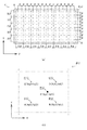
図4(a)に示すように、基板Fには、複数の電子部品の実装点と複数の基準点とが設けられている。基準点は、所定の間隔αでX方向に直線状に並んでいる基準点の列が所定の間隔β毎にY方向に配置されている。つまり、基板Fには、X方向の間隔α、Y方向の間隔βの仮想の格子の各交点に基準点が設けられている。この際、基準点は、実装点と重複しないように設けられている。従って、本発明に係る実装位置補正方法は、実装点を基準点として補正が実施されないので電子部品の実装状態に影響されない。なお、基板Fに設けられる基準点の配置は、本実施形態に限定されるものではなく、基板Fの形状および理論実装位置に応じて任意の位置に設けることができる。
次に、図4(a)に示すように、小領域設定工程において、基板Fには、任意に定めた位置を原点として任意の範囲を複数の小領域E(i)に区切るように仮想線Sが設定される。本実施形態において、基板Fは、その全範囲においてX方向に延びるように複数の仮想線Sが設定され、Y方向に延びるように複数の仮想線Sが設定される。すなわち、基板Fは、X方向に延びる複数の仮想線SとY方向に延びる複数の仮想線Sとによって格子状に区切られた小領域E(i)が設定される。この際、X方向に延びる仮想線Sは、所定の間隔2β(β×2)で隣り合う基準点間の中央に設定される。つまり、X方向に延びる仮想線Sは、2点の基準点毎にY方向に並ぶように設定される。Y方向に延びる仮想線Sは、所定の間隔2α(α×2)で隣り合う基準点間の中央に設定される。つまり、Y方向に延びる仮想線Sは、2点の基準点毎にX方向に並ぶように設定される。これにより、格子状に区切られた基板Fの任意の小領域E(i)には、4点の基準点A(i)・B(i)・C(i)・D(i)が含まれている。
図4(b)に示すように、小領域E(i)に含まれる基準点A(i)は、任意に定めた位置を原点として理論基準点位置A(Xa(i)、Ya(i))に設けられている。同様に、基準点B(i)・C(i)・D(i)は、理論基準点位置B(Xb(i)、Yb(i))・理論基準点位置C(Xc(i)、Yc(i))・理論基準点位置D(Xd(i)、Yd(i))に設けられている。また、小領域E(i)には、電子部品が実装される実装点P(i)が含まれている。小領域E(i)に含まれる実装点P(i)は、任意に定めた位置を原点として理論実装位置P(Xp(i)、Yp(i))に設けられている。なお、基板Fに設定される小領域E(i)は、本実施形態に限定されるものではなく、基板Fの形状、理論基準点位置および理論実装位置に応じて任意の位置に3点以上の基準点が含まれるように設定されていればよい。
図5(a)に示すように、基準点位置測定工程において、基板Fは、8台のカメラ4(図1参照)によってX方向に4分割、Y方向に2分割した範囲がそれぞれ撮影される。各カメラ4によって撮影された基板Fの部分画像V1・V2・V3・・・V6には、複数の小領域E(i)が含まれている。また、基板Fの各部分画像V1・V2・V3・・・V6は、隣接するカメラ4によって撮影された基板Fの部分画像V1・V2・V3・・・V6の一部と重複している(図5(a)における薄墨部分)。従って、部分画像V1・V2・V3・・・V6の一部と重複している部分(以下、単に「重複部分」と記す)には、複数の基準点が含まれている。基板Fの各部分画像V1・V2・V3・・・V6は、重複部分に含まれる同一の基準点同士を重ね合わせてつなぎ合わされる。
具体的には、図5(b-1)に示すように、部分画像V1には、小領域P(3)の基準点B(3)と基準点D(3)とが撮影されている。また、図5(b-2)に示すように、部分画像V2には、小領域P(3)の基準点B(3)と基準点D(3)とが撮影されている。つまり、図5(c)に示すように、部分画像V1と部分画像V2とは、重複部分に小領域P(3)の基準点B(3)と基準点D(3)とが含まれている。従って、部分画像V1と部分画像V2とは、互いの基準点B(3)と基準点D(3)とを重ね合わせることで適切に結合することができる。このようにして、基板Fの部分画像V1・V2・V3・・・V6は、重複部分の基準点を利用して互いに結合される。この結果、基板Fの全体画像Vが基板Fの部分画像から形成される。そして、形成された基板Fの全体画像Vにおいて、各基準点の実基準点位置が予め定められた任意の基準点を原点として測定される。なお、本実施形態において、各カメラ4によって撮影された基板Fの部分画像V1・V2・V3・・・V6は、それぞれ異なるカメラ4が撮影したものであるがこれに限定されるものではなく、一のカメラ4が複数の異なる任意の場所を撮影してもよい。
変形量算出工程において、基板Fは、小領域E(i)に含まれる4点の基準点A(i)・B(i)・C(i)・D(i)のうち任意の3点の実基準点位置を用いて小領域E(i)毎にその変形量を算出する。変形量算出工程は、移動量算出工程、伸縮量算出工程および回転角度算出工程を含む。
図6に示すように、移動量算出工程において、基板Fに設定された任意の小領域E(i)では、小領域E(i)に含まれる基準点A(i)の理論基準点位置A(Xa(i)、Ya(i))が小領域E(i)の変形により実基準点位置A´(Xa(i)´、Ya(i)´)に移動した際のX方向の移動量ΔXa(i)=(Xa(i)-Xa(i)´)とY方向の移動量ΔYa(i)=(Ya(i)-Ya(i)´)とからなる移動量M(ΔXa(i)、ΔYa(i))が算出される。
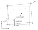
図7(a)に示すように、伸縮量算出工程において、基板Fに設定された任意の小領域E(i)では、小領域E(i)に含まれる4点の基準点A(i)・B(i)・C(i)・D(i)のうち一方向(本実施形態においてX方向)に最も離間している2点の基準点A(i)と基準点B(i)とについて、理論基準点位置A(Xa(i)、Ya(i))と理論基準点位置B(Xb(i)、Yb(i))との間の理論距離L(i)ab、および実基準点位置A´(Xa(i)´、Ya(i)´)と実基準点位置B´(Xb(i)´、Yb(i)´)との間の実距離L(i)a´b´が算出される。同様にして、図7(b)に示すように、任意の小領域E(i)に含まれる4点の基準点のうち他方向(本実施形態においてY方向)に最も離間している2点の基準点A(i)と基準点C(i)とについて、理論基準点位置A(Xa(i)、Ya(i))と理論基準点位置C(Xc(i)、Yc(i))との間の理論距離L(i)ac、および実基準点位置A´(Xa(i)´、Ya(i)´)と実基準点位置C´(Xc(i)´、Yc(i)´)との間の実距離L(i)a´c´が算出される。
一般に、点P(Xp、Yp)と点Q(Xq、Yq)との距離Lpqは、以下の数1に基づいて算出される。

従って、理論距離L(i)abは、理論基準点位置A(Xa(i)、Ya(i))と理論基準点位置B(Xb(i)、Yb(i))とから数3に基づいて算出される。実距離L(i)a´b´は、実基準点位置A´(Xa(i)´、Ya(i)´)と実基準点位置B´(Xb(i)´、Yb(i)´)とから数3に基づいて算出される。同様にして、理論距離L(i)acは、理論基準点位置A(Xa(i)、Ya(i))と理論基準点位置C(Xc(i)、Yc(i))とから数1に基づいて算出される。実距離L(i)a´c´は、実基準点位置A´(Xa(i)´、Ya(i)´)と実基準点位置C´(Xc(i)´、Yc(i)´)とから数3に基づいて算出される。実距離L(i)a´b´は、小領域E(i)のX方向の伸縮に伴って、基準点A(i)に対して基準点B(i)が移動することにより定まる。すなわち、小領域E(i)のX方向の伸縮量Q(i)xは、理論距離L(i)abと実距離L(i)a´b´との差からが算出される。同様にして、小領域E(i)のY方向の伸縮量Q(i)yは、理論距離L(i)acと実距離L(i)a´c´との差からが算出される。
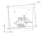
図8に示すように、回転角度算出工程において、基板Fに設定された任意の小領域E(i)では、小領域E(i)に含まれる4点の基準点のうち最も離間している2点の基準点A(i)と基準点B(i)とについて、理論基準点位置A(Xa(i)、Ya(i))と理論基準点位置B(Xb(i)、Yb(i))とを通る理論直線ABのx軸に対する角度θ(i)ab、および実基準点位置A´(Xa(i)´、Ya(i)´)と実基準点位置B´(Xb(i)´、Yb(i)´)とを通る直線の実直線A´B´のx軸に対する角度θ(i)a´b´が算出される。
一般に、点P(Xp、Yp)と点Q(Xq、Yq)とを通る直線PQは以下の数2に基づいて算出される(y軸に平行な直線を除く)。

また、算出された直線PQの式から、直線PQのx軸に対する角度θpqは以下の数3に基づいて算出される。

従って、理論直線ABのx軸に対する角度θ(i)abは、理論基準点位置A(Xa(i)、Ya(i))と理論基準点位置B(Xb(i)、Yb(i))とから数2と数3とに基づいて算出される。同様にして、実直線A´B´のx軸に対する角度θ(i)a´b´は、実基準点位置A´(Xa(i)´、Ya(i)´)と実基準点位置B´(Xb(i)´、Yb(i)´)とから数2と数3とに基づいて算出される。実直線A´B´のx軸に対する角度θ(i)a´b´は、小領域E(i)の回転に伴って理論直線ABが回転することにより定まる。すなわち、小領域E(i)の回転角度θ(i)は、理論直線ABのx軸に対する角度θ(i)abと実直線A´B´のx軸に対する角度θ(i)a´b´との差からが算出される。本実施形態において、基準点A(i)と基準点B(i)とはx軸に対して平行に設定されているため、理論直線ABのx軸に対する角度θ(i)ab=0である。従って、小領域E(i)の回転角度θ(i)=角度θ(i)a´b´である。
図9に示すように、実装位置補正工程において、基板Fに設定された任意の小領域E(i)に含まれる実装点P(i)は、移動量算出工程において算出した小領域E(i)の移動量M(ΔXa(i)、ΔYa(i))だけ移動しているとして、理論実装位置P(Xp(i)、Yp(i))に移動量M(ΔXa(i)、ΔYa(i))を加える移動量補正が行われる。すなわち、理論基準点A(i)の移動に伴って実装点P(i)が移動される。これにより、実装点P(i)の理論実装位置P(Xp(i)、Yp(i))は、移動量補正実装位置P(Xp(i)+ΔXa(i)、Yp(i)+ΔYa(i))に補正される(図における点P(i)m)。
次に、実装点P(i)は、伸縮量算出工程において算出した小領域E(i)のX方向の伸縮量Q(i)xおよびY方向の伸縮量Q(i)yだけ伸縮移動しているとして、移動量補正実装位置P(Xp(i)+ΔXa(i)、Yp(i)+ΔYa(i))にX方向の伸縮量Q(i)xおよびY方向の伸縮量Q(i)yを加える伸縮量補正が行われる。これにより、実装点P(i)の移動量補正実装位置P(Xp(i)+ΔXa(i)、Yp(i)+ΔYa(i))は、伸縮量補正実装位置P(Xp(i)+ΔXa(i)+Q(i)x、Yp(i)+ΔYa(i)+Q(i)y)に補正される(図における点P(i)q)。
最後に、実装点P(i)は、回転角度算出工程において算出した小領域E(i)の回転角度θ(i)だけ回転しているとして、伸縮量補正実装位置P(Xp(i)+ΔXa(i)+Q(i)x、Yp(i)+ΔYa(i)+Q(i)y)に基準点A(i)を回転中心として回転角度θ(i)だけ回転させる回転量補正が行われる。
一般に点P(Xp、Yp)を回転中心として点Q(Xq、Yq)を角度θだけ回転させた点R(Xr、Yr)は、点Pを原点(0、0)とした場合の点Q(Xq、Yq)を座標Qc(Xqc、Yqc)とすると以下の数4に基づいて算出される。

従って、回転中心である基準点A(i)を原点(0、0)とした場合の実装点P(i)の座標である座標Pc(Xp(i)+ΔXa(i)+Q(i)x-Xa(i)、Yp(i)+ΔYa(i)+Q(i)y-Ya(i))を座標Pc(Xpc、Ypc)とすると、実装点P(i)の伸縮量補正実装位置P(Xp(i)+ΔXa(i)+Q(i)x、Yp(i)+ΔYa(i)+Q(i)y)は、数4に基づいて実実装位置P´(Xa(i)+cosθ(i)*Xpc-sinθ(i)*Ypc、Ya(i)+sinθ(i)*Xpc+cosθ(i)*Ypc)に補正される(図におけるP´(Xp(i)´、Yp(i)´))。
以上より、実装位置補正装置1は、小領域設定工程として、制御装置6の小領域データテーブルT1に基板Fの任意の範囲を区切って設定される複数の小領域E(i)の情報が格納される。実装位置補正装置1は、基準点位置測定工程として、基板Fの部分画像V1・V2・V3・・・V6から全体画像Vを形成し、予め定められた任意の基準点を原点として各基準点の実基準点位置が測定される。そして、実装位置補正装置1は、小領域E(i)の移動量算出工程において、小領域E(i)に含まれる基準点A(i)の移動量M(ΔXa(i)、ΔYa(i))を算出し、伸縮量算出工程において、一方向に並ぶ2点の基準点A(i)と基準点B(i)との距離の変化から小領域E(i)のX方向の伸縮量Q(i)xを算出し、他の方向に並ぶ2点の基準点A(i)と基準点C(i)との距離の変化から小領域E(i)のY方向の伸縮量Q(i)yを算出し、回転角度算出工程において、一の方向に並ぶ2点の基準点A(i)と基準点B(i)とを通る理論直線ABの傾きの変化から小領域E(i)の回転角度θ(i)を算出する。最後に、実装位置補正装置1は、実装位置補正工程において、小領域E(i)の移動量M(ΔXa(i)、ΔYa(i))とX方向の伸縮量Q(i)xおよびY方向の伸縮量Q(i)yと回転角度θ(i)とから実装点P(i)の理論実装位置P(Xp(i)、Yp(i))を補正する。
このように構成することで、カメラ4で一括して撮影された複数の基準点の実基準点位置に基づいて、小領域E(i)を一つの単位として算出した変形量に基づいて実装点P(i)の理論実装位置P(Xp(i)、Yp(i))が補正される。これにより、基板Fに局所的な変形が生じても電子部品の実装点P(i)の理論実装位置P(Xp(i)、Yp(i))を適切に補正することができる。また、3点の基準点によって実装点P(i)の理論実装位置P(Xp(i)、Yp(i))を補正するので、先行技術文献のように4点の基準点を用いた場合よりも計算処理速度を短縮することができる。
F 基板
A(i) 基準点
E(i) 小領域
P(i) 実装点
ΔXa(i) X方向移動量
ΔYa(i) Y方向移動量
Q(i)x X方向伸縮量
Q(i)y Y方向伸縮量
θ(i) 回転角度
Xp(i) 理論実装位置X座標
Yp(i) 理論実装位置Y座標
A(i) 基準点
E(i) 小領域
P(i) 実装点
ΔXa(i) X方向移動量
ΔYa(i) Y方向移動量
Q(i)x X方向伸縮量
Q(i)y Y方向伸縮量
θ(i) 回転角度
Xp(i) 理論実装位置X座標
Yp(i) 理論実装位置Y座標
Claims (3)
- 変形した基板に対する電子部品の実装位置補正方法であって、
複数の基準点が設けられた基板の任意の領域をそれぞれが複数の基準点を含む複数の小領域に区切る小領域設定工程と、
複数の基準点の実基準点位置を測定する基準点位置測定工程と、
予め定められている理論基準点位置と実基準点位置とから小領域毎にその移動量と伸縮量と回転角度とを算出する変形量算出工程と、
小領域の移動量と伸縮量と回転角度とから予め定められている電子部品の理論実装位置を補正する実装位置補正工程と、
を含む実装位置補正方法。 - 前記小領域設定工程において、前記複数の小領域に3点以上の前記基準点がそれぞれ含まれるように区切り、
前記変形量算出工程が、
小領域に含まれる基準点の理論基準点位置および実基準点位置から小領域の移動量を算出する移動量算出工程と、
選択した一の方向に並ぶ2点の基準点の理論距離と一の方向に並ぶ2点の基準点の実距離とから小領域のX方向の伸縮量を算出し、小領域に含まれる基準点のうち他の方向に並ぶ2点の基準点を選択し、選択した他の方向に並ぶ2点の基準点の理論距離と他の方向に並ぶ2点の基準点の実距離とから小領域のY方向の伸縮量を算出する伸縮量算出工程と、
小領域に含まれる基準点のうち一の方向に並ぶ2点の基準点を選択し、選択した基準点の前記理論基準点位置を通る理論直線のX軸に対する角度と選択した基準点の前記実基準点位置を通る実直線のX軸に対する角度とから小領域の回転角度を算出する回転角度算出工程と、
を含む請求項1に記載の実装位置補正方法。 - 変形した基板に対する電子部品の実装位置補正装置であって、
複数の基準点が設けられた基板の任意の領域を撮影する撮影手段と、
基準点の理論基準点位置の情報を格納する理論基準点データテーブル、基板の任意の領域を区切った複数の小領域の情報を格納する小領域データテーブル、電子部品の理論実装位置の情報を格納する実装位置データテーブルおよび基準点の実基準点位置の情報を格納する実基準点データテーブル、を有し、撮影手段が撮影した基板の画像から基準点の実基準点位置を取得するとともに実基準点データテーブルに格納し、理論基準点データテーブルに格納した理論基準点位置と実基準点データテーブルに格納した実基準点位置と小領域データテーブルに格納した小領域の情報とから小領域毎にその移動量と伸縮量と回転角度とを算出し、理論実装位置データテーブルに格納した電子部品の理論実装位置が含まれる小領域の移動量と伸縮量と回転角度とからその電子部品の理論実装位置を補正する制御装置と、
を具備する実装位置補正装置。
Applications Claiming Priority (2)
| Application Number | Priority Date | Filing Date | Title |
|---|---|---|---|
| JP2015054070A JP2016174110A (ja) | 2015-03-17 | 2015-03-17 | 実装位置補正方法および実装位置補正装置 |
| JP2015-054070 | 2015-03-17 |
Publications (1)
| Publication Number | Publication Date |
|---|---|
| WO2016147781A1 true WO2016147781A1 (ja) | 2016-09-22 |
Family
ID=56918925
Family Applications (1)
| Application Number | Title | Priority Date | Filing Date |
|---|---|---|---|
| PCT/JP2016/054497 Ceased WO2016147781A1 (ja) | 2015-03-17 | 2016-02-17 | 実装位置補正方法および実装位置補正装置 |
Country Status (2)
| Country | Link |
|---|---|
| JP (1) | JP2016174110A (ja) |
| WO (1) | WO2016147781A1 (ja) |
Cited By (4)
| Publication number | Priority date | Publication date | Assignee | Title |
|---|---|---|---|---|
| JP2018082096A (ja) * | 2016-11-17 | 2018-05-24 | ハンファテクウィン株式会社Hanwha Techwin Co.,Ltd. | 電子部品実装システム及び電子部品実装方法 |
| CN111788878A (zh) * | 2018-03-23 | 2020-10-16 | 株式会社富士 | 元件安装装置 |
| CN114025509A (zh) * | 2021-11-12 | 2022-02-08 | 江西昶龙科技有限公司 | 一种用于电子元件校正的安装装置 |
| CN114497317A (zh) * | 2020-11-11 | 2022-05-13 | 合肥欣奕华智能机器股份有限公司 | 一种确定基板的绑定位置的方法、装置、设备和存储介质 |
Families Citing this family (2)
| Publication number | Priority date | Publication date | Assignee | Title |
|---|---|---|---|---|
| JP7780739B2 (ja) * | 2021-09-17 | 2025-12-05 | パナソニックIpマネジメント株式会社 | 部品装着装置、補正データの生成方法および部品装着システム |
| WO2025141803A1 (ja) * | 2023-12-27 | 2025-07-03 | 株式会社Fuji | 対基板作業機、および補正データ作成方法 |
Citations (2)
| Publication number | Priority date | Publication date | Assignee | Title |
|---|---|---|---|---|
| JPH08102599A (ja) * | 1994-09-30 | 1996-04-16 | Sanyo Electric Co Ltd | 基板位置検出装置 |
| JPH1051198A (ja) * | 1996-05-08 | 1998-02-20 | Tenryu Technic:Kk | 電子部品実装方法 |
-
2015
- 2015-03-17 JP JP2015054070A patent/JP2016174110A/ja active Pending
-
2016
- 2016-02-17 WO PCT/JP2016/054497 patent/WO2016147781A1/ja not_active Ceased
Patent Citations (2)
| Publication number | Priority date | Publication date | Assignee | Title |
|---|---|---|---|---|
| JPH08102599A (ja) * | 1994-09-30 | 1996-04-16 | Sanyo Electric Co Ltd | 基板位置検出装置 |
| JPH1051198A (ja) * | 1996-05-08 | 1998-02-20 | Tenryu Technic:Kk | 電子部品実装方法 |
Cited By (7)
| Publication number | Priority date | Publication date | Assignee | Title |
|---|---|---|---|---|
| JP2018082096A (ja) * | 2016-11-17 | 2018-05-24 | ハンファテクウィン株式会社Hanwha Techwin Co.,Ltd. | 電子部品実装システム及び電子部品実装方法 |
| CN111788878A (zh) * | 2018-03-23 | 2020-10-16 | 株式会社富士 | 元件安装装置 |
| CN111788878B (zh) * | 2018-03-23 | 2021-09-21 | 株式会社富士 | 元件安装装置 |
| CN114497317A (zh) * | 2020-11-11 | 2022-05-13 | 合肥欣奕华智能机器股份有限公司 | 一种确定基板的绑定位置的方法、装置、设备和存储介质 |
| CN114497317B (zh) * | 2020-11-11 | 2023-09-12 | 合肥欣奕华智能机器股份有限公司 | 一种确定基板的绑定位置的方法、装置、设备和存储介质 |
| CN114025509A (zh) * | 2021-11-12 | 2022-02-08 | 江西昶龙科技有限公司 | 一种用于电子元件校正的安装装置 |
| CN114025509B (zh) * | 2021-11-12 | 2023-06-02 | 江西昶龙科技有限公司 | 一种用于电子元件校正的安装装置 |
Also Published As
| Publication number | Publication date |
|---|---|
| JP2016174110A (ja) | 2016-09-29 |
Similar Documents
| Publication | Publication Date | Title |
|---|---|---|
| WO2016147781A1 (ja) | 実装位置補正方法および実装位置補正装置 | |
| US9441957B2 (en) | Three-dimensional shape measuring apparatus | |
| US9348240B2 (en) | Mask pattern alignment method and system | |
| US8271919B2 (en) | Method for correcting image rendering data, method for rendering image, method for manufacturing wiring board, and image rendering system | |
| JP5478122B2 (ja) | 位相シフト画像撮像装置、部品移載装置および位相シフト画像撮像方法 | |
| TWI734111B (zh) | 標記位置檢測裝置、描繪裝置以及標記位置檢測方法 | |
| CN102354086A (zh) | 一种精密移动平台的正交性实时标定方法 | |
| CN105388708B (zh) | 投影曝光装置和方法、光掩模以及基板的制造方法 | |
| CN108700409A (zh) | 三维测量装置 | |
| TW201608345A (zh) | 描繪裝置 | |
| CN102564304B (zh) | 形成于薄片上的图案的位置及形状测定装置 | |
| KR20190125475A (ko) | 포토에칭 장치 및 방법 | |
| JP6343524B2 (ja) | 投影露光装置 | |
| JP2009192693A (ja) | パターン描画装置 | |
| JP2017134375A (ja) | 露光装置及び露光方法 | |
| TW202113346A (zh) | 圖案測定裝置、圖案測定裝置中之傾斜度算出方法及圖案測定方法 | |
| CN110174077B (zh) | 3维测量装置、电子部件安装装置及3维测量方法 | |
| KR20130022415A (ko) | 측정장치 및 이의 보정방법 | |
| US20170307366A1 (en) | Projection device, measuring apparatus, and article manufacturing method | |
| KR101340336B1 (ko) | 비전검사장치 | |
| JP2008065034A (ja) | 描画装置およびアライメント方法 | |
| JP6457295B2 (ja) | 部品判定装置 | |
| TWI544275B (zh) | 校正光束圖案化的方向和位置的方法 | |
| TWI620999B (zh) | 描繪裝置、曝光描繪裝置、描繪方法及記錄媒體 | |
| JP7526540B1 (ja) | 3次元形状計測方法 |
Legal Events
| Date | Code | Title | Description |
|---|---|---|---|
| 121 | Ep: the epo has been informed by wipo that ep was designated in this application |
Ref document number: 16764611 Country of ref document: EP Kind code of ref document: A1 |
|
| NENP | Non-entry into the national phase |
Ref country code: DE |
|
| 122 | Ep: pct application non-entry in european phase |
Ref document number: 16764611 Country of ref document: EP Kind code of ref document: A1 |