WO2016147221A1 - 光走査装置のキャリブレーション方法およびキャリブレーション装置 - Google Patents
光走査装置のキャリブレーション方法およびキャリブレーション装置 Download PDFInfo
- Publication number
- WO2016147221A1 WO2016147221A1 PCT/JP2015/001516 JP2015001516W WO2016147221A1 WO 2016147221 A1 WO2016147221 A1 WO 2016147221A1 JP 2015001516 W JP2015001516 W JP 2015001516W WO 2016147221 A1 WO2016147221 A1 WO 2016147221A1
- Authority
- WO
- WIPO (PCT)
- Prior art keywords
- light
- optical
- optical fiber
- receiving surface
- calibration
- Prior art date
- Legal status (The legal status is an assumption and is not a legal conclusion. Google has not performed a legal analysis and makes no representation as to the accuracy of the status listed.)
- Ceased
Links
Images


Classifications
-
- G—PHYSICS
- G02—OPTICS
- G02B—OPTICAL ELEMENTS, SYSTEMS OR APPARATUS
- G02B26/00—Optical devices or arrangements for the control of light using movable or deformable optical elements
- G02B26/08—Optical devices or arrangements for the control of light using movable or deformable optical elements for controlling the direction of light
- G02B26/10—Scanning systems
- G02B26/103—Scanning systems having movable or deformable optical fibres, light guides or waveguides as scanning elements
-
- A—HUMAN NECESSITIES
- A61—MEDICAL OR VETERINARY SCIENCE; HYGIENE
- A61B—DIAGNOSIS; SURGERY; IDENTIFICATION
- A61B1/00—Instruments for performing medical examinations of the interior of cavities or tubes of the body by visual or photographical inspection, e.g. endoscopes; Illuminating arrangements therefor
- A61B1/00002—Operational features of endoscopes
- A61B1/00004—Operational features of endoscopes characterised by electronic signal processing
- A61B1/00006—Operational features of endoscopes characterised by electronic signal processing of control signals
-
- A—HUMAN NECESSITIES
- A61—MEDICAL OR VETERINARY SCIENCE; HYGIENE
- A61B—DIAGNOSIS; SURGERY; IDENTIFICATION
- A61B1/00—Instruments for performing medical examinations of the interior of cavities or tubes of the body by visual or photographical inspection, e.g. endoscopes; Illuminating arrangements therefor
- A61B1/00002—Operational features of endoscopes
- A61B1/00057—Operational features of endoscopes provided with means for testing or calibration
-
- A—HUMAN NECESSITIES
- A61—MEDICAL OR VETERINARY SCIENCE; HYGIENE
- A61B—DIAGNOSIS; SURGERY; IDENTIFICATION
- A61B1/00—Instruments for performing medical examinations of the interior of cavities or tubes of the body by visual or photographical inspection, e.g. endoscopes; Illuminating arrangements therefor
- A61B1/00163—Optical arrangements
- A61B1/00172—Optical arrangements with means for scanning
-
- A—HUMAN NECESSITIES
- A61—MEDICAL OR VETERINARY SCIENCE; HYGIENE
- A61B—DIAGNOSIS; SURGERY; IDENTIFICATION
- A61B1/00—Instruments for performing medical examinations of the interior of cavities or tubes of the body by visual or photographical inspection, e.g. endoscopes; Illuminating arrangements therefor
- A61B1/04—Instruments for performing medical examinations of the interior of cavities or tubes of the body by visual or photographical inspection, e.g. endoscopes; Illuminating arrangements therefor combined with photographic or television appliances
- A61B1/044—Instruments for performing medical examinations of the interior of cavities or tubes of the body by visual or photographical inspection, e.g. endoscopes; Illuminating arrangements therefor combined with photographic or television appliances for absorption imaging
-
- A—HUMAN NECESSITIES
- A61—MEDICAL OR VETERINARY SCIENCE; HYGIENE
- A61B—DIAGNOSIS; SURGERY; IDENTIFICATION
- A61B1/00—Instruments for performing medical examinations of the interior of cavities or tubes of the body by visual or photographical inspection, e.g. endoscopes; Illuminating arrangements therefor
- A61B1/06—Instruments for performing medical examinations of the interior of cavities or tubes of the body by visual or photographical inspection, e.g. endoscopes; Illuminating arrangements therefor with illuminating arrangements
- A61B1/0661—Endoscope light sources
- A61B1/0684—Endoscope light sources using light emitting diodes [LED]
-
- A—HUMAN NECESSITIES
- A61—MEDICAL OR VETERINARY SCIENCE; HYGIENE
- A61B—DIAGNOSIS; SURGERY; IDENTIFICATION
- A61B1/00—Instruments for performing medical examinations of the interior of cavities or tubes of the body by visual or photographical inspection, e.g. endoscopes; Illuminating arrangements therefor
- A61B1/06—Instruments for performing medical examinations of the interior of cavities or tubes of the body by visual or photographical inspection, e.g. endoscopes; Illuminating arrangements therefor with illuminating arrangements
- A61B1/07—Instruments for performing medical examinations of the interior of cavities or tubes of the body by visual or photographical inspection, e.g. endoscopes; Illuminating arrangements therefor with illuminating arrangements using light-conductive means, e.g. optical fibres
-
- G—PHYSICS
- G02—OPTICS
- G02B—OPTICAL ELEMENTS, SYSTEMS OR APPARATUS
- G02B1/00—Optical elements characterised by the material of which they are made; Optical coatings for optical elements
- G02B1/10—Optical coatings produced by application to, or surface treatment of, optical elements
- G02B1/11—Anti-reflection coatings
-
- G—PHYSICS
- G02—OPTICS
- G02B—OPTICAL ELEMENTS, SYSTEMS OR APPARATUS
- G02B23/00—Telescopes, e.g. binoculars; Periscopes; Instruments for viewing the inside of hollow bodies; Viewfinders; Optical aiming or sighting devices
- G02B23/24—Instruments or systems for viewing the inside of hollow bodies, e.g. fibrescopes
- G02B23/2407—Optical details
- G02B23/2461—Illumination
- G02B23/2469—Illumination using optical fibres
Definitions
- the present invention relates to a calibration method and a calibration device for an optical scanning device.
- An optical scanning device in which an optical fiber is periodically oscillated to scan outgoing light on an object.
- an optical scanning endoscope an object is irradiated with illumination light by vibrating an optical fiber so as to draw a spiral trajectory whose amplitude periodically expands and contracts. Then, detected light such as reflected light and fluorescence obtained by irradiation of the illumination light is detected at each predetermined detection timing, and an image is generated by assigning a pixel position to the detected signal. For this reason, in order to generate an image by the optical scanning endoscope apparatus, information on the irradiation position of the illumination light at each time point of the optical scanning is necessary.
- a method of determining the irradiation position of the illumination light based on the elapsed time from the start of vibration of the optical fiber is used. Since there are individual differences in the optical scanning endoscope, information on the irradiation position is necessary for each apparatus.
- an optical position detector determines in advance at which time the tip of the optical fiber is located.
- the PSD is a sensor that detects the position of the light spot formed on the light receiving surface. By using this sensor, time series data of the barycentric position of the light spot can be obtained. Thereby, the position irradiated with the illumination light and the elapsed time after the start of vibration can be associated with each optical scanning device.
- the method of performing calibration using polynomial approximation can improve relatively small noise.
- correction using approximate equations is possible. In many cases, it is not possible.
- a smooth trajectory is calculated based on data including noise.
- the noise generated by PSD itself is not reduced, it is a fundamental solution. It was difficult to improve the accuracy significantly.
- Such a problem is not limited to an optical scanning endoscope, and similarly occurs in an optical scanning microscope, an optical scanning projector, and the like that perform scanning by vibrating an optical fiber.
- an object of the present invention which has been made paying attention to these points, is to provide a calibration method and a calibration device for an optical scanning device that suppresses noise generation in an optical position detector (PSD) and improves image distortion. It is to provide.
- an optical scanning device comprising: an optical fiber having a tip portion supported so as to be capable of vibration; and an actuator for driving the tip portion of the optical fiber in a direction perpendicular to the optical axis of the optical fiber,
- the detection step is performed using interference fringe suppression means that suppresses interference fringes generated on an optical path reaching the optical position detector.
- the interference fringe suppressing means suppresses interference fringes by reducing reflection that may be generated by the optical position detector.
- the calibration method includes a light transmitting member for protecting the light receiving surface facing the light receiving surface of the optical position detector, and the interference fringe suppression means is at least one of the light transmitting members. This surface can be in a low reflection state.
- a light transmitting member for protecting the light receiving surface is provided opposite to the light receiving surface of the optical position detector, and the interference fringe suppression means is provided between the light receiving surface of the optical position detector and the light transmitting member.
- a medium having a refractive index closer to the light transmission member than air may be filled.
- the interference fringe suppressing means may suppress the generation of interference fringes in the optical position detector by supplying light having low coherence to the optical fiber.
- An optical scanning device calibration apparatus comprising: an optical fiber having a tip portion supported so as to be capable of vibration; and an actuator for driving the tip portion of the optical fiber in a direction perpendicular to the optical axis of the optical fiber, A control unit for controlling the actuator; An optical position detector for detecting the position of light emitted from the tip of the optical fiber; A storage unit for storing calibration data based on position information of the emitted light output from the optical position detector; Interference fringe suppression means for suppressing interference fringes generated on the optical path reaching the optical position detector; It is characterized by providing.
- the calibration device includes a light transmitting member for protecting the light receiving surface facing the light receiving surface of the optical position detector, and the interference fringe suppressing means is at least one of the light transmitting members. It can be set as the anti-reflective film provided in the surface.
- the calibration device includes a light transmission member for protecting the light receiving surface facing the light receiving surface of the optical position detector, and the interference fringe suppressing means includes the light receiving surface of the light position detecting means and the light receiving surface.
- a medium having a refractive index closer to that of the light transmission member than that of air may be filled between the light transmission member and the light transmission member.
- the calibration device may include a light source that supplies light having low coherence to the optical fiber, and the light source may function as the interference fringe suppression means.
- the light source having low coherence is an SLD or an LED.
- calibration refers to the position of the fiber tip of the optical scanning device that scans by vibrating the fiber or the irradiation spot of the light emitted from the fiber tip at which time. Is acquired in advance using an optical position detector or the like.
- An “optical scanning device” is a device that scans light on an object by vibrating the tip of an optical fiber supported so as to vibrate. The optical scanning endoscope, optical scanning microscope, optical A scanning projection apparatus and the like are included.
- the “optical position detector” is a detector that detects the position of the light spot on the detection surface, and is also referred to as PSD hereinafter.
- the “interference fringe suppression means” is a component that suppresses interference fringes generated in the PSD.
- the anti-reflection film or microstructure formed on the surface of the PSD protective glass examples include a high refractive index medium filled between the light receiving surface and the protective glass, and a light source that emits light having low coherence.
- the “light transmissive member” is a member having a wavelength characteristic that transmits illumination light used for calibration, and is, for example, glass or light transmissive resin.
- the “low reflection state” means a state in which reflection occurring at the interface of the light transmitting member is suppressed, specifically, a state in which an antireflection film is formed, a state in which a fine structure of light wavelength order is formed, etc. Is included.
- the optical position detector (PSD)
- PSD optical position detector
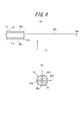
- FIG. 4A is a side view of the actuator of the optical scanning endoscope apparatus together with an optical fiber for illumination
- FIG. 4B is a cross-sectional view taken along line AA of FIG.
- PSD of FIG. It is a flowchart which shows the procedure of a calibration. It is sectional drawing of PSD of the calibration apparatus which concerns on 2nd Embodiment. It is a figure which shows an example of the distortion of the image by the conventional calibration method.
- the present inventors have examined the accuracy of PSD position detection using a laser scanning microscope (LSM) that performs optical scanning using a galvanometer mirror pair in order to investigate the cause of errors in position data that occur during calibration. Went. Specifically, a PSD light-receiving surface was placed in the vicinity of the observation position of the laser scanning microscope, and a microscope image was obtained by scanning the laser. A scanning mechanism using a galvanometer mirror used in a laser scanning microscope (LSM) has an accurate and stable scanning locus, and thus an image with accurate positional information can be obtained.
- LSM laser scanning microscope
- interference fringes were generated inside the PSD, and the amount of light in the microscopic image changed depending on the position. Further, it was also observed that there were two types of interference fringes observed: interference fringes with narrow intervals and interference fringes with wide intervals.
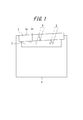
- FIG. 1 is a diagram for explaining the generation of interference fringes in a PSD, and is a cross-sectional view of the light receiving surface of the PSD as viewed from the side.
- a protective glass 3 for protecting the light receiving surface 2 is provided opposite to the light receiving surface 2 of the PSD 1.
- the protective glass 3 is slightly inclined with respect to the light receiving surface 2 due to manufacturing errors.
- FIG. 1 shows the inclination of the protective glass 3 with emphasis.
- the light receiving surface 2 of the PSD 1 is a silicon surface and generates strong reflected light with respect to incident light. Therefore, in addition to the reflected light, it is considered that interference fringes derived from reflection by the both surfaces 3a and 3b of the protective glass 3 are generated.
- the narrow interference fringes are due to the inclination between the light receiving surface 2 and the protective glass 3. It is estimated that the interference fringes with a wide interval are due to the fact that both surfaces 3a and 3b of the protective glass 3 are slightly non-parallel.
- the PSD 1 has an appropriate light amount range for performing a correct measurement. Therefore, if the light amount during observation varies greatly, the correct light spot position is not output. Therefore, the present inventors are convinced that there is a high possibility that the cause of the detection error of PSD1 is an interference fringe caused by reflected light from the light receiving surface and the protective glass, and as described in the following embodiment, the interference fringe is explained. Measures are taken to suppress this.
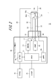
- FIG. 2 is a block diagram showing a state in which the optical scanning endoscope 30 is connected to the calibration device according to the first embodiment of the present invention.
- the calibration device includes a calibration device body 10 and a PSD 20.
- a display device 18 such as a display and an input device 19 such as a keyboard, a mouse, and / or a touch panel are connected to the calibration device body 10 as necessary.
- the optical scanning endoscope 30 is connected to the calibration apparatus main body 10 by a connection unit 31.
- the optical scanning endoscope 30 to be calibrated is a so-called scope portion of the endoscope apparatus, and an illumination optical fiber 33 inserted through the optical scanning endoscope 30 and an illumination optical fiber.
- An actuator 34 that drives the distal end portion 33a of 33, a drive signal line 35 that transmits a drive signal to the actuator 34, and a memory 36 that is built in the optical scanning endoscope 30 (for example, the connection portion 31).
- the optical scanning endoscope 30 is inserted with a light receiving optical fiber 37 (see FIG. 3) that receives and transmits the detected light such as reflected light or fluorescence caused by illumination light irradiation.
- the optical scanning endoscope 30 is connected to a control device main body (not shown) of the optical scanning endoscope apparatus by a connection unit 31 and used for generating an endoscopic image.
- the optical scanning endoscope apparatus main body includes an optical source that supplies light to the optical scanning endoscope 30, a driving circuit for driving the actuator 34, and an image from pixel data received by the optical scanning endoscope 30.
- An image processing circuit to be generated is provided.
- Such an optical scanning endoscope apparatus is disclosed in, for example, Japanese Patent Application Publication Nos. 2014-44265 and 2014-145941.
- the optical scanning endoscope 30 is normally distributed separately from the main body of the control device, and the calibration device of the present invention is mainly for calibrating the optical scanning endoscope 30 at the time of product shipment. Is.
- the calibration device main body 10 is configured to be connectable to the connection portion 31 of the optical scanning endoscope 30 in the same manner as the control device main body during endoscope observation.
- the calibration apparatus main body 10 includes a control unit 11 that controls the entire calibration apparatus main body 10, a light source unit 12 that supplies illumination light for calibration to the optical scanning endoscope 30, and an optical scanning endoscope.
- a drive circuit 13 that drives the actuator 34 of the mirror 30, an arithmetic circuit 14 that receives and processes the output from the PSD 20, and a storage unit 15 that stores calibration data output from the arithmetic circuit 14 are provided.
- the light source unit 12 includes a calibration light source such as a laser diode or a DPSS laser (semiconductor excitation solid laser).
- a calibration light source such as a laser diode or a DPSS laser (semiconductor excitation solid laser).
- a plurality of light sources that emit light having different wavelengths may be used to obtain a color image.
- the light emission timing of the light source unit 12 is controlled by the control unit 11.
- the light emitted from the light source unit 12 enters the illumination optical fiber 16 and is coupled to the illumination optical fiber 33 of the optical scanning endoscope 30 at the connection unit 31.
- the illumination optical fibers 16 and 33 single mode optical fibers can be used.
- the drive circuit 13 supplies a drive signal similar to that during endoscope observation to the actuator 34 of the optical scanning endoscope 30. As will be described later, when the tip of the illumination optical fiber 33 is driven by a piezoelectric element, the drive circuit 13 supplies a drive voltage for the piezoelectric element. The output of the drive circuit 13 is supplied to the drive signal line 17. The drive signal line 17 is connected to the drive signal line 35 of the optical scanning endoscope 30 at the connection portion 31. The drive circuit 13 is also controlled by the control unit 11 to start driving.
- the arithmetic circuit 14 acquires a detection signal corresponding to the irradiation position on the light receiving surface of the illumination light output from the PSD 20 via the detection signal line 21, and uses this signal as a coordinate value (x, y) of the irradiation position. Convert. Further, the arithmetic circuit 14 associates the converted coordinate value (x, y) with the elapsed time from the start of driving of the drive circuit 13 by the control unit 11. If necessary, the arithmetic circuit 14 may smooth the error of the coordinate position of the illumination light using polynomial approximation or the like.
- the irradiation light irradiation position information associated with the elapsed time calculated by the arithmetic circuit 14 is configured to be stored in the storage unit 15 as calibration data.
- FIG. 3 is a cross-sectional view of the distal end portion 32a (the portion indicated by the wavy line) of the insertion portion 32 of the optical scanning endoscope 30 of FIG.
- the distal end portion 32a of the insertion portion 32 of the optical scanning endoscope 30 includes an actuator 34, projection lenses 38a and 38b, an illumination optical fiber 33 passing through the central portion, and a plurality of light receiving optical fibers 37 passing through the outer peripheral portion. Consists of.
- the light receiving optical fiber 37 is used for detecting light to be detected during endoscope observation and is not used for calibration.
- the actuator 34 includes an actuator tube 40 fixed inside the insertion portion 32 by an attachment ring 39, and a fiber holding member 41 and piezoelectric elements 42a to 42d arranged in the actuator tube 40 (FIGS. 4A and 4B). ))).
- the illumination optical fiber 33 is supported by a fiber holding member 41 and a swinging portion 33b supported from the fiber holding member 41 to the distal end portion 33a so as to vibrate. Further, the projection lenses 38 a and 38 b are arranged at the forefront of the insertion portion 32. The projection lenses 38a and 38b are configured to substantially condense the laser light emitted from the distal end portion 33a of the illumination optical fiber 33 onto the observation object. Therefore, the PSD 20 is positioned so that the light receiving surface coincides with the light collection position.
- the projection lens is not limited to a two-lens configuration, and may be configured by one lens or a plurality of other lenses.
- FIG. 4A and 4B are views showing the actuator 34 of the optical scanning endoscope 30 together with the illumination optical fiber 33.
- FIG. 4A is a side view
- FIG. 4B is an AA view of FIG. It is sectional drawing.
- the illumination optical fiber 33 passes through the center of the fiber holding member 41 having a prismatic shape, and is thereby fixed and held by the fiber holding member 41.
- the four side surfaces of the fiber holding member 41 are oriented in the + Y direction and the + X direction, which are perpendicular to the + Z direction, which is the optical axis direction of the optical fiber, and in the opposite directions.
- the pair of piezoelectric elements 42a and 42c for driving in the Y direction are fixed in the + Y direction and the ⁇ Y direction of the fiber holding member 41, and the pair of piezoelectric elements 42b and 42d for driving in the X direction are fixed in the + X and ⁇ X directions. Is fixed. Piezoelectric elements 42b and 42d arranged opposite to each other with the fiber holding member 41 interposed therebetween cause the fiber holding member 41 to bend when one of the piezoelectric elements 42b and 42d expands, and repeats this to generate vibration in the X direction. Close. The same applies to the vibration in the Y direction.
- the drive circuit 13 applies an oscillating voltage with the same frequency to the piezoelectric elements 42b and 42d for driving in the X direction and the piezoelectric elements 42a and 42c for driving in the Y direction, or an oscillating voltage with a different frequency, It can be driven by vibration.
- the swinging portion 33b of the illumination optical fiber 33 shown in FIGS. 3 and 4 vibrates. Since the tip portion 33a vibrates and deflects, the laser light emitted from the tip portion 33a scans the light receiving surface 22 of the PSD 20 (see FIG. 5).
- an oscillating voltage having the same frequency in the X and Y directions and a phase difference of approximately 90 ° and an amplitude varying between 0 and the maximum value is applied.
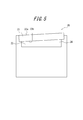
- FIG. 5 is a cross-sectional view of the PSD 20 of FIG. 2 as viewed from a direction along the light receiving surface 22 (a direction substantially perpendicular to the optical path of incident light incident on the center of the light receiving surface 22).
- the illumination light emitted from the illumination optical fiber 33 enters from above. That is, the PSD 20 in FIG. 2 is one in which the light receiving surface 22 of the PSD 20 in FIG.
- the PSD 20 includes a light receiving surface 22 and a protective glass 23 disposed so as to face and separate from the light receiving surface 22.
- the light receiving surface 22 is formed on a silicon substrate and usually has a high reflectance.
- An air layer 24 is formed between the light receiving surface 22 and the protective glass 23.
- the protective glass 23 It is difficult to accurately arrange the light receiving surface 22 and the protective glass 23 in a parallel state, and the protective glass 23 has an undesired inclination with respect to the light receiving surface 22 (in FIG. 5, the inclination is emphasized). . Further, the protective glass 23 itself has a slight wedge angle, and the outer side surface 23 a facing the tip end portion 32 a of the illumination optical fiber 33 and the inner side surface 23 b facing the light receiving surface 22 of the PSD 20 are not completely parallel.
- an antireflection film (AR coating) is formed on at least one of the outer surface 23a and the inner surface 23b.
- an antireflection film is formed on both the inner side surface 23a and the outer side surface 23b.
- the antireflection film prevents light reflected by at least one of the surfaces 23 a and 23 b of the protective glass 23 from interfering with illumination light directly incident on the light receiving surface 22. That is, the antireflection film functions as interference fringe suppression means that suppresses interference fringes generated on the optical path reaching the PSD 20.
- the user of the present calibration apparatus that performs calibration connects the connection unit 31 of the optical scanning endoscope 30 to the calibration apparatus main body 10 (step S01).
- the illumination optical fiber 16 and the drive signal line 17 of the calibration apparatus body 10 are connected to the illumination optical fiber 33 and the drive signal line 35 of the optical scanning endoscope 30, respectively.
- the user fixes the distal end portion 32a of the insertion portion 32 of the optical scanning endoscope 30, and the light receiving surface of the PSD 20 on the condensing surface on which the illumination light emitted from the distal end portion 32a forms a spot.
- the PSD 20 is arranged so that 22 matches (step S02).
- the detection signal line 21 of the PSD 20 is connected to the arithmetic circuit 14 of the calibration apparatus body 10.
- the control unit 11 activates the actuator 34 by the drive circuit 13 and starts spiral scanning while emitting illumination light from the light source unit 12.
- the PSD 20 sequentially detects the locus of the spot position of the illumination light over at least one period of spiral scanning (step S03).
- an antireflection film is formed on at least one of the outer side surface 23a and the inner side surface 23b of the protective glass 23 of the PSD 20, the generation of interference fringes on the light receiving surface 22 is suppressed. As a result, the amount of illumination light incident on the PSD does not vary depending on the scanning position, and the spot position of the illumination light can be accurately detected.
- the PSD 20 sequentially outputs a detection signal (for example, a voltage value corresponding to the spot position) corresponding to the detected light spot position to the arithmetic circuit 14.
- the arithmetic circuit 14 receives information on the elapsed time after the activation of the drive circuit 13 from the control unit 11, and associates the coordinate information of the spot position calculated from the detection signal with the time information as calibration data. Further, depending on the case, processing such as correction of the detection error of the PSD 20, smoothing of the detected locus, detection of an abnormal value of data, and the like are performed.
- the calibration data calculated by the arithmetic circuit 14 is stored in the storage unit 15 in the calibration apparatus main body 10 (step S04).
- the storage unit 15 can be a storage device inside the calibration apparatus main body 10. Alternatively, the storage unit 15 may be a portable storage medium (such as a memory card) that can be attached to and detached from the calibration apparatus main body 10.
- step S05 when the storage of the calibration data in the storage unit 15 is completed, the calibration data in the storage unit 15 is output to the memory 36 inside the optical scanning endoscope 30 (step S05).
- the storage unit 15 is a portable storage medium
- the user removes it from the calibration apparatus main body 10 and inserts it as a memory 36 in a predetermined location of the optical scanning endoscope 30. In that case, this removable storage medium attachment / detachment operation may be performed after the end of the next step S06.
- the user removes the connection part 31 of the optical scanning endoscope 30 from the calibration apparatus body 10 (step S06).
- the optical scanning endoscope 30 holds the calibration data in the memory 36.
- the optical scanning endoscope 30 is connected to a control device body having a light source, a drive circuit, and an image processing unit.
- the main body of the control apparatus reads calibration data from the memory 36 of the optical scanning endoscope 30, and generates an image by associating the acquired pixel value with the pixel position based on the calibration data.
- highly accurate calibration data is stored in the optical scanning endoscope 30 by performing calibration by the calibration procedure using the calibration device.
- an antireflection film is formed on at least one of the outer surface 23a and the inner surface 23b of the protective glass 23, it is possible to suppress the occurrence of interference fringes on the light receiving surface 22 and inaccurate output of the PSD 20. it can.
- an image with less distortion can be generated.
- the distal end portion 32a of the insertion portion 32 that performs optical scanning is very small, and it is difficult to arrange a sensor or the like that detects the position of the distal end portion 33a of the illumination optical fiber 33 at the distal end portion. It is. For this reason, the calibration method of the present invention is particularly suitable when applied to the optical scanning endoscope 30.
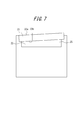
- FIG. 7 is a cross-sectional view of the PSD 20 of the calibration apparatus according to the second embodiment.
- a gel whose refractive index is closer to the refractive index of the protective glass than the air between the light receiving surface 22 of the PSD 20 and the protective glass 23. Or the like 25 is filled.
- the refractive index difference between the protective glass 23 and the medium 25 is made smaller than the refractive index difference between the protective glass 23 and air, thereby reducing the generation of reflected light.
- the refractive index of the medium 25 is preferably closer to the refractive index of the protective glass 23.
- the occurrence of interference fringes on the light receiving surface 22 is reduced by reducing the reflection between the protective glass 23 and the medium 25.
- the occurrence of interference fringes on the light receiving surface 22 is reduced by reducing the reflection between the protective glass 23 and the medium 25.
- a PSD similar to the PSD 1 having no antireflection film shown in FIG. 1 is used in place of the PSD 20 of the first embodiment, and an SLD is used for the light source unit 12 in FIG. (Super Luminescent Diode), a light source with low coherence such as LED is used.
- SLD Super Luminescent Diode
- a light source with low coherence such as LED is used.
- Other configurations are the same as those of the first embodiment, and the description thereof is omitted.
- PSD having no antireflection film may be used in the same manner as PSD20. In that case, interference fringes can be further suppressed by the effects of both the antireflection film and the low-coherence light source, so that a higher effect can be obtained.
- the scanning trajectory of the optical scanning device is not limited to spiral scanning.
- the present invention can be applied to raster scanning and Lissajous scanning.
- the method of driving the optical fiber of the optical scanning device is not limited to the method using a piezoelectric element, and the actuator at the tip of the optical fiber can be configured by an electromagnetic driving method using an electromagnetic coil and a permanent magnet. . In that case, the drive circuit controls the current instead of controlling the voltage applied to the actuator.
- control unit, the light source unit, the drive circuit, the arithmetic circuit, and the storage unit are built in the same calibration apparatus body, but these may be separate hardware.
- the member that protects the light receiving surface of the PSD is made of glass, but is not limited to this, and a light-transmitting resin or the like can also be used.
- the above embodiment is applied to calibration before shipment of the optical scanning device.
- the present invention is not limited to this, and can also be applied to calibrate the optical scanning device after starting use.
- a calibration device main body dedicated for calibration is provided separately from the control device main body for observation, but the function of the calibration device main body is built in the control device main body for observation and used. A person may be able to perform calibration at any time.
- the optical scanning device is not limited to the optical scanning endoscope, and can be applied to an optical scanning microscope or an optical scanning projection device (projector) that scans a fiber.
- the optical scanning endoscope that is an optical scanning device does not include a light source and a drive circuit.
- the present invention can also be applied to an optical scanning device that incorporates these. it can.
- the calibration device includes at least a control unit of the calibration device main body connected to the optical scanning device, a PSD that suppresses the generation of interference fringes, and a storage device that stores position information detected by the PSD.
- the optical scanning device may be driven to scan the fiber under the control of the unit, the position of the light spot may be detected by PSD, and stored in the storage device in association with the timing information.
- various modifications are possible for the configuration of the calibration apparatus.
- the calibration unit main body is provided with the storage unit and the calibration data is temporarily stored.
- the calibration device main body is not provided with the storage unit, and the calibration calculated by the arithmetic circuit is provided.
- the image data may be directly output to the memory of the optical scanning device.
- the calibration device and the calibration method according to the present invention can be used for calibration of an optical scanning device, and can be suitably used particularly for calibration before product shipment.
- SYMBOLS 10 Calibration apparatus main body 11 Control part 12 Light source part 13 Drive circuit 14 Arithmetic circuit 15 Memory
Landscapes
- Health & Medical Sciences (AREA)
- Life Sciences & Earth Sciences (AREA)
- Physics & Mathematics (AREA)
- Surgery (AREA)
- Optics & Photonics (AREA)
- Engineering & Computer Science (AREA)
- Medical Informatics (AREA)
- General Health & Medical Sciences (AREA)
- Pathology (AREA)
- Nuclear Medicine, Radiotherapy & Molecular Imaging (AREA)
- Biomedical Technology (AREA)
- Heart & Thoracic Surgery (AREA)
- Biophysics (AREA)
- Molecular Biology (AREA)
- Animal Behavior & Ethology (AREA)
- Radiology & Medical Imaging (AREA)
- Public Health (AREA)
- Veterinary Medicine (AREA)
- General Physics & Mathematics (AREA)
- Astronomy & Astrophysics (AREA)
- Signal Processing (AREA)
- Microelectronics & Electronic Packaging (AREA)
- Endoscopes (AREA)
- Instruments For Viewing The Inside Of Hollow Bodies (AREA)
Abstract
Description
振動可能に支持された先端部を有する光ファイバと、前記光ファイバの先端部を該光ファイバの光軸に垂直な方向に駆動させるアクチュエータと、を備える光走査装置に適用され、
前記光ファイバの前記先端部からの出射光の位置を検出する光位置検出器を配置する配置ステップと、
前記光ファイバに光を供給するとともに該光ファイバの前記先端部を駆動して、前記光位置検出器により出射光の位置を検出する検出ステップと、
を含む光走査装置のキャリブレーション方法において、
前記検出ステップは、前記光位置検出器に対し到達する光路上で発生する干渉縞を抑制する干渉縞抑制手段を用いて実行されることを特徴とするものである。
振動可能に支持された先端部を有する光ファイバと、前記光ファイバの先端部を該光ファイバの光軸に垂直な方向に駆動させるアクチュエータと、を備える光走査装置のキャリブレーション装置であって、
前記アクチュエータを制御する制御部と、
前記光ファイバの前記先端部からの出射光の位置を検出する光位置検出器と、
前記光位置検出器から出力された出射光の位置情報に基づくキャリブレーションデータを格納する記憶部と、
前記光位置検出器に対し到達する光路上で発生する干渉縞を抑制する干渉縞抑制手段と、
を備えることを特徴とするものである。
図2は、本発明の第1実施の形態に係るキャリブレーション装置に光走査型内視鏡30を接続した状態を示すブロック図である。キャリブレーション装置は、キャリブレーション装置本体10とPSD20とを備える。また、キャリブレーション装置本体10には、必要に応じて、ディスプレイ等の表示装置18や、キーボード、マウス、および/またはタッチパネル等の入力装置19が接続されている。光走査型内視鏡30は、接続部31によりキャリブレーション装置本体10に対して接続される。
すなわち、反射防止膜は、PSD20に対し到達する光路上で発生する干渉縞を抑制する干渉縞抑制手段として機能する。
図7は、第2実施の形態に係るキャリブレーション装置のPSD20の断面図である。第2実施の形態では、保護ガラス23に反射防止膜を形成することに代えて、PSD20の受光面22と保護ガラス23との間に、屈折率が空気よりも保護ガラスの屈折率に近いゲル等の媒質25を充填する。これにより、保護ガラス23と媒質25との屈折率差を、保護ガラス23と空気との屈折率差より小さくして、反射光の発生を軽減したものである。媒質25の屈折率は、保護ガラス23の屈折率により近いことが好ましい。特に、媒質25の屈折率を保護ガラス23の屈折率と一致させることによって、保護ガラス23と媒質25との間の界面での反射を抑止することができる。その他の構成は、第1実施の形態と同様であるので、同一または対応する構成要素には同一参照符号を付して説明を省略する。
本発明の第3実施の形態は、第1実施の形態のPSD20に代えて図1に示した反射防止膜を有さないPSD1と同様のPSDを用い、さらに、図2の光源部12にSLD(Super Luminescent Diode)、LED等の可干渉性の低い光源を使用する。その他の構成は、第1実施の形態と同様とし、説明を省略する。
11 制御部
12 光源部
13 駆動回路
14 演算回路
15 記憶部
16 照明用光ファイバ
17 駆動信号線
18 表示装置
19 入力装置
20 PSD
21 検出信号線
22 受光面
23 保護ガラス
23a 外側面
23b 内側面
24 空気層
25 媒質
30 光走査型内視鏡
31 接続部
32 挿入部
32a 先端部
33 照明用光ファイバ
33a 先端部
33b 揺動部
34 アクチュエータ
35 駆動信号線
36 メモリ
37 受光用光ファイバ
37a 先端部
38a,38b 投影用レンズ
39 取付環
40 アクチュエータ管
41 ファイバ保持部材
42a,42b,42c,42d 圧電素子
Claims (10)
- 振動可能に支持された先端部を有する光ファイバと、前記光ファイバの先端部を該光ファイバの光軸に垂直な方向に駆動させるアクチュエータと、を備える光走査装置に適用され、
前記光ファイバの前記先端部からの出射光の位置を検出する光位置検出器を配置する配置ステップと、
前記光ファイバに光を供給するとともに該光ファイバの前記先端部を駆動して、前記光位置検出器により出射光の位置を検出する検出ステップと、
を含む光走査装置のキャリブレーション方法において、
前記検出ステップは、前記光位置検出器に対し到達する光路上で発生する干渉縞を抑制する干渉縞抑制手段を用いて実行されることを特徴とするキャリブレーション方法。 - 前記干渉縞抑制手段は、前記光位置検出器で発生し得る反射を軽減させることで干渉縞を抑制することを特徴とする、請求項1に記載のキャリブレーション方法。
- 前記光位置検出器の受光面に対向して前記受光面の保護用の光透過部材を設け、前記干渉縞抑制手段は、前記光透過部材の少なくとも一方の面を低反射状態としたものである、請求項2に記載のキャリブレーション方法。
- 前記光位置検出器の受光面に対向して前記受光面の保護用の光透過部材を設け、前記干渉縞抑制手段は、前記光位置検出器の受光面と前記光透過部材との間に、屈折率が空気よりも前記光透過部材に近い媒質を充填して構成されることを特徴とする請求項2に記載のキャリブレーション方法。
- 前記干渉縞抑制手段は、前記光ファイバに可干渉性の低い光を供給することで、前記光位置検出器内での干渉縞の発生を抑制することを特徴とする、請求項1から4の何れか一項に記載のキャリブレーション方法。
- 振動可能に支持された先端部を有する光ファイバと、前記光ファイバの先端部を該光ファイバの光軸に垂直な方向に駆動させるアクチュエータと、を備える光走査装置のキャリブレーション装置であって、
前記アクチュエータを制御する制御部と、
前記光ファイバの前記先端部からの出射光の位置を検出する光位置検出器と、
前記光位置検出器から出力された出射光の位置情報に基づくキャリブレーションデータを格納する記憶部と、
前記光位置検出器に対し到達する光路上で発生する干渉縞を抑制する干渉縞抑制手段と、
を備えることを特徴とするキャリブレーション装置。 - 前記光位置検出器の受光面に対向して該受光面の保護用の光透過部材を備え、前記干渉縞抑制手段は、前記光透過部材の少なくとも一方の面に設けられた反射防止膜であることを特徴とする請求項6に記載のキャリブレーション装置。
- 前記光位置検出器の受光面に対向して該受光面の保護用の光透過部材を備え、前記干渉縞抑制手段は、前記光位置検出手段の受光面と前記光透過部材との間に、屈折率が空気よりも前記光透過部材に近い媒質を充填して構成されることを特徴とする請求項6に記載のキャリブレーション装置。
- 前記光ファイバに可干渉性の低い光を供給する光源を備え、該光源は前記干渉縞抑制手段として機能することを特徴とする請求項6から8の何れか一項に記載のキャリブレーション装置。
- 前記可干渉性の低い光源は、SLDまたはLEDであることを特徴とする請求項9に記載のキャリブレーション装置。
Priority Applications (5)
| Application Number | Priority Date | Filing Date | Title |
|---|---|---|---|
| DE112015006197.5T DE112015006197T5 (de) | 2015-03-18 | 2015-03-18 | Kalibriervorrichtung und Verfahren zum Kalibrieren einer optischen Abtastvorrichtung |
| PCT/JP2015/001516 WO2016147221A1 (ja) | 2015-03-18 | 2015-03-18 | 光走査装置のキャリブレーション方法およびキャリブレーション装置 |
| JP2017505749A JPWO2016147221A1 (ja) | 2015-03-18 | 2015-03-18 | 光走査装置のキャリブレーション方法およびキャリブレーション装置 |
| CN201580077865.0A CN107427184A (zh) | 2015-03-18 | 2015-03-18 | 光扫描装置的校准方法和校准装置 |
| US15/705,364 US20180003953A1 (en) | 2015-03-18 | 2017-09-15 | Calibration apparatus and method for calibrating optical scanning apparatus |
Applications Claiming Priority (1)
| Application Number | Priority Date | Filing Date | Title |
|---|---|---|---|
| PCT/JP2015/001516 WO2016147221A1 (ja) | 2015-03-18 | 2015-03-18 | 光走査装置のキャリブレーション方法およびキャリブレーション装置 |
Related Child Applications (1)
| Application Number | Title | Priority Date | Filing Date |
|---|---|---|---|
| US15/705,364 Continuation US20180003953A1 (en) | 2015-03-18 | 2017-09-15 | Calibration apparatus and method for calibrating optical scanning apparatus |
Publications (1)
| Publication Number | Publication Date |
|---|---|
| WO2016147221A1 true WO2016147221A1 (ja) | 2016-09-22 |
Family
ID=56918499
Family Applications (1)
| Application Number | Title | Priority Date | Filing Date |
|---|---|---|---|
| PCT/JP2015/001516 Ceased WO2016147221A1 (ja) | 2015-03-18 | 2015-03-18 | 光走査装置のキャリブレーション方法およびキャリブレーション装置 |
Country Status (5)
| Country | Link |
|---|---|
| US (1) | US20180003953A1 (ja) |
| JP (1) | JPWO2016147221A1 (ja) |
| CN (1) | CN107427184A (ja) |
| DE (1) | DE112015006197T5 (ja) |
| WO (1) | WO2016147221A1 (ja) |
Cited By (1)
| Publication number | Priority date | Publication date | Assignee | Title |
|---|---|---|---|---|
| CN111033113A (zh) * | 2017-08-18 | 2020-04-17 | 统雷有限公司 | 基于结晶磷光体的宽带光源 |
Families Citing this family (4)
| Publication number | Priority date | Publication date | Assignee | Title |
|---|---|---|---|---|
| EP3562649B1 (en) * | 2016-12-29 | 2020-09-23 | 3D Systems, Inc. | Sensor that simulates resin optical properties |
| CN108803010A (zh) * | 2017-12-07 | 2018-11-13 | 成都理想境界科技有限公司 | 一种提升光纤扫描图像画质的方法及装置 |
| MX2020010395A (es) | 2018-04-05 | 2020-10-22 | Ericsson Telefon Ab L M | Selección de tamaño de bloque de transporte para transmisión de datos temprana. |
| CN118541071A (zh) * | 2021-08-10 | 2024-08-23 | 杭安医学科技(杭州)有限公司 | 一种扫描光纤内镜探头和扫描光纤内镜 |
Citations (1)
| Publication number | Priority date | Publication date | Assignee | Title |
|---|---|---|---|---|
| JP2012147831A (ja) * | 2011-01-17 | 2012-08-09 | Hoya Corp | 走査位置補正装置 |
Family Cites Families (3)
| Publication number | Priority date | Publication date | Assignee | Title |
|---|---|---|---|---|
| US20070247639A1 (en) * | 2004-05-10 | 2007-10-25 | Koninklijke Philips Electronics, N.V. | Device and Method for Optical Precision Measurement |
| WO2013111604A1 (ja) * | 2012-01-26 | 2013-08-01 | オリンパス株式会社 | 光走査型観察装置 |
| JP2013178417A (ja) * | 2012-02-29 | 2013-09-09 | Hoya Corp | キャリブレーション装置 |
-
2015
- 2015-03-18 JP JP2017505749A patent/JPWO2016147221A1/ja not_active Ceased
- 2015-03-18 DE DE112015006197.5T patent/DE112015006197T5/de not_active Withdrawn
- 2015-03-18 WO PCT/JP2015/001516 patent/WO2016147221A1/ja not_active Ceased
- 2015-03-18 CN CN201580077865.0A patent/CN107427184A/zh active Pending
-
2017
- 2017-09-15 US US15/705,364 patent/US20180003953A1/en not_active Abandoned
Patent Citations (1)
| Publication number | Priority date | Publication date | Assignee | Title |
|---|---|---|---|---|
| JP2012147831A (ja) * | 2011-01-17 | 2012-08-09 | Hoya Corp | 走査位置補正装置 |
Cited By (1)
| Publication number | Priority date | Publication date | Assignee | Title |
|---|---|---|---|---|
| CN111033113A (zh) * | 2017-08-18 | 2020-04-17 | 统雷有限公司 | 基于结晶磷光体的宽带光源 |
Also Published As
| Publication number | Publication date |
|---|---|
| JPWO2016147221A1 (ja) | 2018-01-11 |
| CN107427184A (zh) | 2017-12-01 |
| DE112015006197T5 (de) | 2017-11-02 |
| US20180003953A1 (en) | 2018-01-04 |
Similar Documents
| Publication | Publication Date | Title |
|---|---|---|
| CN105899120B (zh) | 光的扫描轨迹的计算方法以及光扫描装置 | |
| US20180003953A1 (en) | Calibration apparatus and method for calibrating optical scanning apparatus | |
| WO2015182137A1 (ja) | 光走査型内視鏡装置 | |
| EP2789968A1 (en) | Shape-measuring device | |
| JP2014018556A (ja) | キャリブレーション装置 | |
| CN107407802A (zh) | 光扫描装置的驱动条件设定方法和驱动条件设定装置 | |
| WO2014188719A1 (ja) | 光走査ユニット、光走査型観察装置、および光ファイバ走査装置 | |
| CN105849550A (zh) | 光声显微镜装置 | |
| JP6416277B2 (ja) | 光走査型内視鏡装置 | |
| JP2014508292A (ja) | 表面を高精度で測定する方法及び装置 | |
| US20180003945A1 (en) | Method for measuring scanning pattern of optical scanning apparatus, apparatus for measuring scanning pattern, and method for calibrating image | |
| JP2014094121A (ja) | 光伝達装置及び光学素子 | |
| JP6778435B2 (ja) | 歯周ポケット検査装置 | |
| US20180007335A1 (en) | Scanning observation apparatus and image display method of scanning observation apparatus | |
| JP4261216B2 (ja) | 走査型共焦点プローブ | |
| JP2012147831A (ja) | 走査位置補正装置 | |
| WO2016208004A1 (ja) | 走査型内視鏡システム | |
| JP2004101438A (ja) | レーザ発生装置、画像読取装置及び画像検査装置 | |
| CN106796172B (zh) | Oct装置用光检测模块及oct装置 | |
| JP2021087973A (ja) | レーザ加工装置 | |
| KR102884172B1 (ko) | 구강 구조물의 단층 촬영 방법 | |
| JP2021169978A (ja) | 傾斜端を有する光ファイバの出射角測定装置、及び出射角測定方法 | |
| TW202509420A (zh) | 用於測量晶圓的裝置和方法 | |
| CN110678290A (zh) | 用于反射或透射扫描仪射束的扫描头设备和方法、具有扫描头设备的扫描设备和扫描仪 | |
| JP6804260B2 (ja) | 検査装置および変位量検出方法 |
Legal Events
| Date | Code | Title | Description |
|---|---|---|---|
| 121 | Ep: the epo has been informed by wipo that ep was designated in this application |
Ref document number: 15885321 Country of ref document: EP Kind code of ref document: A1 |
|
| ENP | Entry into the national phase |
Ref document number: 2017505749 Country of ref document: JP Kind code of ref document: A |
|
| WWE | Wipo information: entry into national phase |
Ref document number: 112015006197 Country of ref document: DE |
|
| 122 | Ep: pct application non-entry in european phase |
Ref document number: 15885321 Country of ref document: EP Kind code of ref document: A1 |