WO2016144024A1 - 신호 수신 장치 - Google Patents
신호 수신 장치 Download PDFInfo
- Publication number
- WO2016144024A1 WO2016144024A1 PCT/KR2016/001860 KR2016001860W WO2016144024A1 WO 2016144024 A1 WO2016144024 A1 WO 2016144024A1 KR 2016001860 W KR2016001860 W KR 2016001860W WO 2016144024 A1 WO2016144024 A1 WO 2016144024A1
- Authority
- WO
- WIPO (PCT)
- Prior art keywords
- signal
- digital
- carrier
- feedback
- divided
- Prior art date
- Legal status (The legal status is an assumption and is not a legal conclusion. Google has not performed a legal analysis and makes no representation as to the accuracy of the status listed.)
- Ceased
Links
Images




Classifications
-
- H—ELECTRICITY
- H04—ELECTRIC COMMUNICATION TECHNIQUE
- H04L—TRANSMISSION OF DIGITAL INFORMATION, e.g. TELEGRAPHIC COMMUNICATION
- H04L27/00—Modulated-carrier systems
- H04L27/18—Phase-modulated carrier systems, i.e. using phase-shift keying
- H04L27/22—Demodulator circuits; Receiver circuits
- H04L27/227—Demodulator circuits; Receiver circuits using coherent demodulation
- H04L27/2275—Demodulator circuits; Receiver circuits using coherent demodulation wherein the carrier recovery circuit uses the received modulated signals
-
- H—ELECTRICITY
- H04—ELECTRIC COMMUNICATION TECHNIQUE
- H04L—TRANSMISSION OF DIGITAL INFORMATION, e.g. TELEGRAPHIC COMMUNICATION
- H04L27/00—Modulated-carrier systems
-
- H—ELECTRICITY
- H04—ELECTRIC COMMUNICATION TECHNIQUE
- H04L—TRANSMISSION OF DIGITAL INFORMATION, e.g. TELEGRAPHIC COMMUNICATION
- H04L27/00—Modulated-carrier systems
- H04L27/18—Phase-modulated carrier systems, i.e. using phase-shift keying
- H04L27/22—Demodulator circuits; Receiver circuits
- H04L27/227—Demodulator circuits; Receiver circuits using coherent demodulation
-
- H—ELECTRICITY
- H04—ELECTRIC COMMUNICATION TECHNIQUE
- H04L—TRANSMISSION OF DIGITAL INFORMATION, e.g. TELEGRAPHIC COMMUNICATION
- H04L27/00—Modulated-carrier systems
- H04L27/0014—Carrier regulation
- H04L2027/0024—Carrier regulation at the receiver end
-
- H—ELECTRICITY
- H04—ELECTRIC COMMUNICATION TECHNIQUE
- H04L—TRANSMISSION OF DIGITAL INFORMATION, e.g. TELEGRAPHIC COMMUNICATION
- H04L27/00—Modulated-carrier systems
- H04L27/0014—Carrier regulation
- H04L2027/0044—Control loops for carrier regulation
- H04L2027/0053—Closed loops
Definitions
- the present invention relates to a signal receiving apparatus, and more particularly, to a signal receiving apparatus for recovering a carrier signal from a modulated signal and detecting a digital signal transmitted through the modulated signal using the recovered carrier signal and the modulated signal.
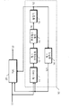
- FIG. 1 is a block diagram showing a conventional signal receiving apparatus.
- the carrier recovery unit 10 for recovering the carrier signal (S2) from the modulated signal (S1) modulated by the PSK (Phase Shift Keying) method, the modulated signal (S1) and the carrier signal (S2) It includes a digital signal generator 20 for outputting a digital signal (S3) using.
- the carrier recovery unit 10 may be configured based on a comparison result of the first phase frequency detector 11 and the first PFD 11 comparing the frequency and phase of the modulated signal S 1 and the first divided signal S 21.
- the first charge pump 12 outputting one pumping voltage Vp1, the low pass filter 15 filtering the first pumping voltage Vp1 and outputting the control voltage Vc, and the carrier according to the control voltage Vc.
- An oscillator 13 for outputting the signal S2 and a first divider 14 for dividing the carrier signal S2 and outputting the first divided signal S21 are included.
- the digital signal generator 20 may be implemented as a TDC (Time to Digital Converter).
- the digital signal generator 20 outputs the digital signal S3 using the first divided signal S21 and the modulated signal S1.
- the carrier recovery unit 10 initially performs a locking operation to recover the carrier signal S2 from the modulated signal S1.
- the modulated signal S1 is shifted in phase in response to the data signal.
- phase of the carrier signal S2 changes along the phase of the modulation signal S1.
- the phase of the carrier signal S2 is preferably initially locked.
- the conventional carrier recovery unit 10 reduces the amount of change in the control voltage Vc even when the phase of the modulation signal S1 is changed by increasing the capacitance of the capacitor included in the low pass filter 15.
- phase of the carrier signal S2 is changed along with the phase of the modulation signal S1, so that the digital signal generator 20 cannot output the correct digital signal S3.
- the present technology provides a signal receiving apparatus that maintains an initial locked state of a carrier signal by feedback controlling a carrier recovery unit using an output digital signal.
- a signal receiving apparatus includes: a digital signal generator configured to generate a digital signal that varies according to a difference between a frequency or a phase of a modulated signal and a carrier signal; And a carrier recovery unit for recovering a carrier signal from the modulated signal but including a feedback control unit for controlling a phase change of the carrier signal using a digital signal.
- the carrier recovery unit may be configured to control voltages generated in response to a phase or frequency difference between the first divided signal and the modulated signal, which have the same period as the carrier signal or divide the carrier signal. Accordingly, the oscillator outputs a carrier signal, but the feedback controller may adjust the control voltage according to the digital signal.
- the carrier recovery unit includes a control code generated in response to a phase or frequency difference between the first divided signal and the modulated signal having the same period as that of the carrier signal or the divided signal of the carrier signal. Accordingly, the digital oscillator outputs a carrier signal, but the feedback controller may change the value of the control code according to the digital signal.
- the signal receiving apparatus uses the output digital signal to feedback control the carrier recovery unit to maintain the initial locked state of the carrier signal.
- the carrier recovery unit when the carrier recovery unit is implemented in a digital form by applying the present technology, the area of the carrier signal is not only reduced by using a capacitor, but also the feedback control can be performed immediately according to the output of the digital signal. As a result, it is possible to suppress the phenomenon that changes accordingly.
- FIG. 1 is a block diagram of a conventional signal receiving apparatus.
- FIG. 2 is a block diagram of a signal receiving apparatus according to an embodiment of the present invention.
- FIG. 3 is a circuit diagram of the first PFD of FIG.
- FIG. 4 is a circuit diagram of an eleventh charge pump, a twelfth charge pump and a filter of FIG.
- FIG. 5 is a detailed block diagram of the feedback signal generator of FIG. 2.
- FIG. 5 is a detailed block diagram of the feedback signal generator of FIG. 2.
- FIG. 6 is a waveform diagram illustrating an operation of a feedback signal generator of FIG. 5.
- FIG. 8 is a block diagram of a signal receiving apparatus according to another embodiment of the present invention.
- FIG. 9 is a block diagram of a signal receiving apparatus according to another embodiment of the present invention.
- FIG. 10 is a detailed block diagram of the feedback control unit and the digital filter of FIG. 9; FIG.
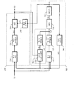
- FIG. 2 is a block diagram of a signal receiving apparatus according to an embodiment of the present invention.
- the signal receiving apparatus uses a carrier recovery unit 100 for recovering a carrier signal S2 from a received modulated signal S1 and a digital signal using a modulated signal S1 and a carrier signal S2. It includes a digital signal generator 200 for outputting a signal (S3).
- the carrier recovery unit 100 includes a configuration of an analog phase locked loop.
- the carrier recovery unit 100 pumps a first pumping voltage according to a signal output from the first PFD 110 and the first PFD 110 comparing the frequency and phase of the modulation signal S1 and the first divided signal S21.
- the carrier signal S2 is applied according to the eleventh charge pump 121 for adjusting Vp1, the filter 150 for filtering the first pumping voltage Vp1 to output the control voltage Vc, and the control voltage Vc.
- the oscillator 130 outputs a first divider 140 for dividing the carrier signal S2 and outputting the first divided signal S21.
- the carrier recovery unit 100 further includes a feedback control unit 160 that adjusts the first pumping voltage Vp1 according to the digital signal S3.
- the feedback control unit 160 adjusts the feedback signal generator 170 outputting the feedback signal FB according to the digital signal S3 and the twelfth charge pump adjusting the first pumping voltage Vp1 according to the feedback signal FB. (122).
- the oscillator 130 and the first divider 140 may be implemented with components known in the art, a detailed description thereof will be omitted.
- the digital signal generator 200 performs a function of a time to digital converter (TDC).
- TDC time to digital converter
- the digital signal generator 200 generates the digital signal S3 based on the phase difference between the carrier signal S2 and the modulated signal S1.
- the digital signal generator 200 may generate a second pumping voltage according to an output of the second PFD 210 and the second PFD 210, which detects a frequency and a phase difference between the modulated signal S1 and the first divided signal S21.
- ADC analog-to-digital converter
- the digital signal generator 200 detects a phase difference of the modulated signal S1 based on the first divided signal S21, generates a second pumping voltage Vp2 corresponding thereto, and converts it into a digital signal S3.
- the digital signal S3 corresponding to the phase of the modulated signal S1 is output.
- the digital signal generator 200 further includes a second divider 240 for dividing the carrier signal S2 to output the second divided signal S22.
- the ADC 230 outputs the digital signal S3 in synchronization with the second divided signal S21.
- the second charge pump 220 generates the second pumping voltage Vp2 during one period of the second divided signal S22, and the corresponding digital signal S3 is next to the second divided signal S22. Output in cycles.
- the frequency division ratio of the first frequency divider 140 and the second frequency divider 240 may be variously determined according to an embodiment.
- the period of the second divided signal S22 may be selected to be the same as the period of the first divided signal S21 or to be a multiple of the period of the first divided signal S21.
- FIG. 3 is a circuit diagram of the first PFD 110 of FIG. 2.
- the first PFD 110 outputs the first flip-flop 111 outputting the first pumping signal UP according to the carrier signal S1 and the second pumping signal DN according to the first division signal S21.
- the second flip-flop 112 When the second flip-flop 112, the first pumping signal UP, and the second pumping signal DN are all activated, the NAND gate for resetting the first flip-flop 111 and the second flip-flop 112 ( 113).
- the first pumping signal UP has a pulse shape having a high level during a period in which the phase of the modulation signal S1 is earlier than the phase of the first division signal S21, and the second pumping signal DN is formed of the first pumping signal UP.
- One division signal S21 has a pulse shape having a high level during a period in which the phase of the modulation signal S1 is advanced.
- the second PFD 210 may be configured substantially the same as the first PFD 110 except for the type of signal.
- the circuit diagram shown in FIG. 3 is an example of implementing the first PFD 210 or the second PFD 220. In another embodiment, other circuits may be used.
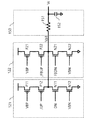
- FIG. 4 is a circuit diagram of the eleventh charge pump 121, the twelfth charge pump 122, and the filter 150.
- the filter 150 may be implemented using the resistor 151 and the capacitor 152 as a low pass filter.
- the illustrated example illustrates a simple type low pass filter, and another embodiment may use a filter having a different structure.
- the eleventh charge pump 121 includes the eleventh PMOS transistor P11, the twelfth PMOS transistor P12, the eleventh NMOS transistor N11, and the twelfth NMOS transistor connected in series between a power supply voltage and a ground voltage. (N12).
- the common drain of the twelfth PMOS transistor P12 and the eleventh NMOS transistor N11 is connected to an input terminal of the filter 150.
- the first bias voltage VBP is input to the gate of the eleventh PMOS transistor P11, and the second bias voltage VBN is input to the gate of the twelfth NMOS transistor N12.
- the signal / UP inverting the first pumping signal UP is input to the gate of the twelfth PMOS transistor P12, and the second pumping signal DN is input to the gate of the eleventh NMOS transistor N11.
- the capacitor 152 is charged to a higher voltage in a period where the first pumping signal UP becomes a high level and the capacitor 152 is discharged to a lower voltage in a period where the second pumping signal DN becomes a high level. .
- the twelfth charge pump 122 includes the twenty-first PMOS transistor P21, the twenty-second PMOS transistor P22, the twenty-first NMOS transistor N21, and the twenty-second NMOS transistor connected in series between a power supply voltage and a ground voltage. (N22).
- the common drain of the twenty-second PMOS transistor P22 and the twenty-first NMOS transistor N21 is connected to an input terminal of the filter 150.
- the first bias voltage VBP is input to the gate of the twenty-first PMOS transistor P21, and the second bias voltage VBN is input to the gate of the twenty-second NMOS transistor N22.
- a signal / FBUP inverting the first feedback signal FBUP is input to the gate of the twenty-second PMOS transistor P22, and a second feedback signal FBDN is input to the gate of the twenty-first NMOS transistor N21.
- the capacitor 152 is charged to a higher voltage in the period when the first feedback signal FBUP is at the high level, and the capacitor 152 is at a lower voltage in the period when the second feedback signal DN is at the high level. Discharged.
- the first feedback signal FBUP and the second feedback signal FBDN input to the twenty-second charge pump 122 correspond to the feedback signal FB output from the feedback signal generator 170.
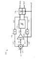
- 5 is a detailed block diagram of the feedback signal generator 170.
- the feedback signal generator 170 includes an adder 171, an accumulator 172, a comparator 173, multipliers 174 and 175, and a flip-flop 176.
- the accumulator 172 and the flip-flop 176 operate in synchronization with the first divided signal S21.
- the comparator 173 compares the accumulator signal S32 output from the accumulator 172 with the threshold point ⁇ and outputs a first signal S33 and a second signal S34.
- both the first signal S33 and the second signal S34 become zero.
- the accumulator signal S32 is positive and the absolute value is greater than or equal to the threshold ⁇ , the first signal S33 is 1 and the second signal S34 is zero.
- the accumulator signal S32 is negative and the absolute value is greater than or equal to the threshold ⁇ , the first signal S33 is zero and the second signal S34 is one.
- the flip-flop 176 latches the first signal S33 in synchronization with the first division signal S21 to output the first feedback signal FBUP, and latches the second signal S34 to latch the second feedback signal FBDN.
- the adder 171 adds the second multiplication signal S36 multiplied by the threshold point ⁇ to the digital signal S3 and the second signal S34, and first multiplication by multiplying the first signal S33 by the threshold point ⁇ .
- the final addition signal S31 obtained by subtracting the signal S35 is provided to the accumulator 172.
- the accumulator 172 updates the stored value by adding the value of the addition signal S31 and the previously stored value in synchronization with the first divided signal S21.
- FIG. 6 is a waveform diagram illustrating an operation of the feedback signal generator 170.
- (A) is the case where the first division signal S21 and the second division signal S22 have the same period
- (B) the period of the second division signal S22 is the same as the period of the first division signal S21. It is a double ship.
- the threshold ⁇ is assumed to be a positive number greater than 16.
- the value of the digital signal S3 at T0 is output as 4, and the accumulator 172 stores ⁇ -6 at T0. Since the accumulator signal S32 is ⁇ -6 and its absolute value is smaller than the threshold, the first signal S33 and the second signal S34 become 0, and the first multiplication signal S35 and the second multiplication signal ( S36) becomes zero. As a result, the addition signal S31 becomes four.
- the value of the digital signal S3 at T1 is seven.
- the accumulator signal S32 becomes ⁇ -2 obtained by adding 4 to the existing value ⁇ -6. Since the absolute value of the accumulator signal S32 is smaller than the threshold, the first signal S33 and the second signal S34 become zero, and the first multiplication signal S35 and the second multiplication signal S36 become zero. . Accordingly, the addition signal S31 becomes seven.
- the flip-flop 176 latches the first signal S33 and the second signal S34 so that the first feedback signal FBUP and the second feedback signal FBDN become zero.
- the value of the digital signal S3 at T2 is -6.
- the accumulator signal S32 becomes ⁇ + 5 by adding 7 to the existing value ⁇ -2. Since the absolute value of the accumulator signal S32 is greater than the threshold and the sign is positive, the first signal S33 is 1, the second signal S34 is 0, the first multiplication signal S35 is ⁇ , and the second multiplication signal. (S36) becomes zero. As a result, the addition signal S31 becomes - ⁇ -6.
- the flip-flop 176 latches the first signal S33 and the second signal S34 so that the first feedback signal FBUP and the second feedback signal FBDN become zero.
- the accumulator signal S32 becomes -1 by adding - ⁇ -6 to the existing value of ⁇ + 5. Since the absolute value of the accumulator signal S32 is smaller than the threshold, the first signal S33 is 0, the second signal S34 is 0, the first multiplication signal S35 is 0, and the second multiplication signal S36. Becomes zero. In addition, the flip-flop 176 latches the first signal S33 and the second signal S34 so that the first feedback signal FBUP is zero and the second feedback signal FBDN is one.
- the accumulator signal S32 becomes -1 by adding - ⁇ -5 to the existing value ⁇ + 5. Since the absolute value of the accumulator signal S32 is smaller than the threshold, the first signal S33 is 0, the second signal S34 is 0, the first multiplication signal S35 is 0, and the second multiplication signal S36. Becomes zero. In addition, the flip-flop 176 latches the first signal S33 and the second signal S34 so that the first feedback signal FBUP is zero and the second feedback signal FBDN is zero.
- the value of the digital signal S3 at T5 is output as -4, and the accumulator 612 stores - ⁇ + 6 at T5. Since the accumulator signal S32 is - ⁇ + 6 and its absolute value is smaller than the threshold, the first signal S33 and the second signal S34 become 0, and the first multiplication signal S35 and the second multiplication signal (S36) becomes zero. As a result, the addition signal S31 becomes -4.
- the value of digital signal S3 is equal to -4.
- the accumulator signal S32 becomes - ⁇ + 2 by adding -4 to the existing value of - ⁇ + 6. Since the absolute value of the accumulator signal S32 is smaller than the threshold, the first signal S33 and the second signal S34 become zero, and the first multiplication signal S35 and the second multiplication signal S36 become zero. . As a result, the addition signal S31 becomes -4.
- the flip-flop 176 latches the first signal S33 and the second signal S34 so that the first feedback signal FBUP and the second feedback signal FBDN become zero.
- the value of the digital signal S3 at T7 is -7.
- the accumulator signal S32 becomes - ⁇ -2 by adding -4 to - ⁇ + 2 which is an existing value. Since the absolute value of the accumulator signal S32 is greater than the threshold and the sign is negative, the first signal S33 is 0, the second signal S34 is 1, the first multiplication signal S35 is 0, and the second multiplication signal. (S36) becomes (alpha). As a result, the addition signal S31 becomes? -7.
- the flip-flop 176 latches the first signal S33 and the second signal S34 so that the first feedback signal FBUP and the second feedback signal FBDN become zero.
- the accumulator signal S32 is -9, which is the existing value of - ⁇ -2 plus ⁇ -7. Since the absolute value of the accumulator signal S32 is smaller than the threshold, the first signal S33 is 0, the second signal S34 is 0, the first multiplication signal S35 is 0, and the second multiplication signal S36. Becomes zero. In addition, the flip-flop 176 latches the first signal S33 and the second signal S34 so that the first feedback signal FBUP is 1 and the second feedback signal FBDN is zero.
- the value of the digital signal S3 at T9 is six.
- the accumulator signal S32 becomes -16 by adding -7 to -9 which is an existing value. Since the absolute value of the accumulator signal S32 is smaller than the threshold, the first signal S33 is 0, the second signal S34 is 0, the first multiplication signal S35 is 0, and the second multiplication signal S36. Becomes zero. Accordingly, the addition signal S31 is six.
- the flip-flop 176 latches the first signal S33 and the second signal S34 so that the first feedback signal FBUP and the second feedback signal FBDN become zero.
- the phase of the carrier signal S2 also increases in the corresponding direction.
- the feedback signal generator 170 reduces the value of the accumulator 172 by the magnitude of the threshold at a time when the absolute value of the accumulator 172 increases in the positive direction beyond the threshold and reduces the second feedback signal FBDN. Activate it. Accordingly, the 21st NMOS transistor N21 of FIG. 4 is turned on and the control voltage Vc is increased to suppress the change in the value of the accumulator 172 from increasing.
- the feedback signal generator 170 increases the value of the accumulator 172 by the magnitude of the threshold at a time when the absolute value of the accumulator 172 exceeds the threshold and increases in the negative direction, and the first feedback signal FBUP. ) Is activated. Accordingly, the twenty-second PMOS transistor N22 of FIG. 4 is turned on and the control voltage Vc is reduced to suppress the increase in the value of the accumulator 172.
- FIG. 7 is a graph illustrating a comparison of the variation of the control voltage Vc in the conventional case and the present invention.
- variable width of the control voltage Vc increases with time while setting the upper and lower limits when the signal having the largest phase difference is continuously generated based on the control voltage Vl immediately after locking.
- the low pass filter 15 requires a large capacity capacitor to suppress large fluctuations in the control voltage Vc.
- the variation range 2Vd of the control voltage Vc is limited by the control of the feedback control unit 160 as compared with the related art.
- the variation range 2Vd may vary depending on the value of the threshold point ⁇ .
- a capacitor 152 having a small capacity enough to suppress a relatively small fluctuation range (2Vd) is sufficient. Accordingly, in one embodiment of the present invention, the problem of increasing the circuit area due to the capacitor 152 is not large.
- FIG. 8 is a block diagram of a signal receiving apparatus according to another embodiment of the present invention.
- the first PFD 110 and the second PFD 210 may include substantially the same components.
- FIG. 8 focuses on this, and does not include the second PFD 210 in FIG. 2, but the second of the eleventh charge pump 121 of the carrier recovery unit 100 and the second of the digital signal generator 200.
- the charge pump 220 commonly receives the output of the first PFD 110.
- the first PFD 110 is located outside the carrier recovery unit 100 and the digital signal generator 200.
- the first PFD 110 is included in the carrier recovery unit 100 or the digital signal generation unit 200 with reference to FIG. 8. Is in an equal relationship with
- FIG. 8 Other components in FIG. 8 are substantially the same as those described with reference to FIGS. 2 to 7, and thus, detailed descriptions thereof will be omitted.
- FIG. 9 is a block diagram of a signal receiving apparatus according to another embodiment of the present invention.
- the carrier recovery unit 1000 includes a configuration of a digital phase locked loop. Since the configuration of the digital signal generator 200 is substantially the same as described above, a detailed description thereof will be omitted.
- the carrier recovery unit 1000 feeds back the TDC 1100 and the comparison code TDCC outputted from the TDC 1100 to compare the frequency and phase of the modulated signal S1 and the first divided signal S21.
- the digital filter 1200 for outputting the control code CC according to the code FC, the digital oscillator 1300 for outputting the carrier signal S2 according to the control code CC, and the carrier signal S2 are divided and divided.
- a first divider 1400 for outputting the divided signal S21 is included.
- the carrier recovery unit 1000 further includes a feedback control unit 1600 for outputting a feedback code FC according to the digital signal S3.
- the TDC 1100, the digital oscillator 1300, and the first divider 1400 have various implementations known in the art, and thus detailed description thereof will be omitted.
- FIG. 10 is a detailed block diagram of the feedback controller 1600 and the digital filter 1200 of FIG. 9.
- the digital filter 1200 of FIG. 10 illustrates a configuration of a general digital filter including a multiplier 1220 and 1230, an adder 1210, 1240 and 1250, and an accumulator 1260.
- the digital filter 1200 may be implemented in various ways according to the embodiment.
- the digital filter 1200 receives the feedback code FC and the comparison code TDCC from the adder 1210 and generates a control code CC.
- the feedback controller 1600 includes a multiplier 1610 that multiplies the digital signal S3 by a constant c to output a feedback code FC.
- the size of the constant c may be determined by the ratio of the resolution of the ADC 230 and the resolution of the TDC 1100.
- the resolution of the ADC 230 refers to a phase difference corresponding to the value 1 of the digital signal S3, and the resolution of the TDC 1100 refers to a phase difference corresponding to the value 1 of the comparison code TDCC.
- the size of the constant c may be set to 1. In another example, when the resolution of the ADC 230 is 4 degrees and the resolution of the TDC 1100 is 8 degrees, the size of the constant c may be set to 0.5.
- the adder 1210 outputs a value obtained by subtracting the feedback code FC from the comparison code TDCC to perform filtering to change the phase of the carrier signal S2 due to the change of the digital signal S3.
- the feedback code FC may be generated in the suppressing direction.
- the carrier signal S2 output from the digital oscillator 1300 maintains its original phase even if the value of the digital signal S3 changes.
- the digital carrier recovery unit 1000 may be advantageous as compared to the analog carrier recovery unit 100 in which time is delayed in feedback since real-time feedback is possible even when the frequency of the carrier signal S2 is high. In addition, since the digital carrier recovery unit 1000 does not need to use a capacitor, the digital carrier recovery unit 1000 may be more advantageous in reducing a circuit area than the analog carrier recovery unit 100.
Landscapes
- Engineering & Computer Science (AREA)
- Computer Networks & Wireless Communication (AREA)
- Signal Processing (AREA)
- Stabilization Of Oscillater, Synchronisation, Frequency Synthesizers (AREA)
Abstract
본 기술에 의한 신호 수신 장치는 변조 신호와 캐리어 신호의 주파수 또는 위상의 차이에 따라 가변하는 디지털 신호를 생성하는 디지털 신호 생성부; 및 변조 신호로부터 캐리어 신호를 복구하되 디지털 신호를 이용하여 캐리어 신호의 위상 변화를 제어하는 피드백 제어부를 포함하는 캐리어 복구부를 포함한다.
Description
본 발명은 신호 수신 장치에 관한 것으로서 보다 구체적으로는 변조된 신호에서 캐리어 신호를 복구하고 복구된 캐리어 신호와 변조된 신호를 이용하여 변조된 신호를 통해 전송된 디지털 신호를 탐지하는 신호 수신 장치에 관한 것이다.
도 1은 종래의 신호 수신 장치를 나타내는 블록도이다.
종래의 신호 수신 장치는 예를 들어 PSK(Phase Shift Keying) 방식으로 변조된 변조 신호(S1)에서 캐리어 신호(S2)를 복구하는 캐리어 복구부(10)와 변조 신호(S1)와 캐리어 신호(S2)를 이용하여 디지털 신호(S3)를 출력하는 디지털 신호 생성부(20)를 포함한다.
캐리어 복구부(10)는 변조 신호(S1)와 제 1 분주 신호(S21)의 주파수 및 위상을 비교하는 제 1 PFD(Phase Frequency Detector, 11), 제 1 PFD(11)의 비교 결과에 따라 제 1 펌핑 전압(Vp1)을 출력하는 제 1 전하 펌프(12), 제 1 펌핑 전압(Vp1)을 필터링하여 제어 전압(Vc)을 출력하는 로우패스 필터(15), 제어 전압(Vc)에 따라 캐리어 신호(S2)를 출력하는 발진기(13), 캐리어 신호(S2)를 분주하여 제 1 분주 신호(S21)를 출력하는 제 1 분주기(14)를 포함한다.
디지털 신호 생성부(20)는 TDC(Time to Digital Converter)로 구현될 수 있다. 디지털 신호 생성부(20)는 제 1 분주 신호(S21)와 변조 신호(S1)를 이용하여 디지털 신호(S3)를 출력한다.
캐리어 복구부(10)는 초기에 로킹 동작을 수행하여 변조 신호(S1)로부터 캐리어 신호(S2)를 복구한다.
로킹 동작이 종료되고 데이터가 전송되는 동안 변조 신호(S1)는 데이터 신호에 대응하여 위상이 쉬프트된다.
캐리어 신호(S2)의 위상은 변조 신호(S1)의 위상을 따라 변하게 되는데 데이터를 정상적으로 복구하기 위하여 캐리어 신호(S2)의 위상은 초기에 로킹된 상태를 유지하는 것이 바람직하다.
종래의 캐리어 복구부(10)는 로우패스 필터(15)에 포함되는 캐패시터의 용량을 크게 함으로써 변조 신호(S1)의 위상이 변하더라도 제어 전압(Vc)의 변화량을 작게 한다.
그러나 캐패시터의 용량이 증가할수록 그 면적이 증가하여 회로를 소형화하는데 어려움이 있다. 또한 캐패시터의 용량이 크더라도 위상이 쉬프트된 변조 신호(S1)가 지속적으로 입력되면 제어 전압(Vc)이 일정 수준 이상으로 변하게 된다.
이에 따라 캐리어 신호(S2)의 위상이 변조 신호(S1)의 위상을 따라 변하게 되어 디지털 신호 생성부(20)에서 올바른 디지털 신호(S3)를 출력할 수 없게 된다.
본 기술은 출력된 디지털 신호를 이용하여 캐리어 복구부를 피드백 제어함으로써 캐리어 신호의 위상이 초기의 로킹된 상태를 유지하도록 하는 신호 수신 장치를 제공한다.
본 발명의 일 실시예에 의한 신호 수신 장치는 변조 신호와 캐리어 신호의 주파수 또는 위상의 차이에 따라 가변하는 디지털 신호를 생성하는 디지털 신호 생성부; 및 변조 신호로부터 캐리어 신호를 복구하되 디지털 신호를 이용하여 캐리어 신호의 위상 변화를 제어하는 피드백 제어부를 포함하는 캐리어 복구부를 포함한다
본 발명의 일 실시예에 의한 신호 수신 장치에서 캐리어 복구부는 캐리어 신호와 동일한 주기를 갖거나 캐리어 신호를 분주한 신호인 제 1 분주 신호와 변조 신호의 위상 또는 주파수 차이에 대응하여 생성되는 제어 전압에 따라 캐리어 신호를 출력하는 발진기를 포함하되 피드백 제어부는 디지털 신호에 따라 제어 전압을 조절할 수 있다.
본 발명의 일 실시예에 의한 신호 수신 장치에서 캐리어 복구부는 캐리어 신호와 동일한 주기를 갖거나 캐리어 신호를 분주한 신호인 제 1 분주 신호와 변조 신호의 위상 또는 주파수 차이에 대응하여 생성되는 제어 코드에 따라 캐리어 신호를 출력하는 디지털 발진기를 포함하되 피드백 제어부는 디지털 신호에 따라 제어 코드의 값을 변경시킬 수 있다.
본 기술에 의한 신호 수신 장치는 출력된 디지털 신호를 이용하여 캐리어 복구부를 피드백 제어함으로써 캐리어 신호의 위상이 초기의 로킹된 상태를 유지하도록 한다.
본 기술을 적용하여 캐리어 복구부를 아날로그 형태로 구현하는 경우 종래에 사용하던 대용량의 캐패시터에 비하여 작은 용량의 캐패시터를 사용할 수 있어 회로의 면적을 감소시킬 수 있다.
또한 본 기술을 적용하여 캐리어 복구부를 디지털 형태로 구현하는 경우에는 캐패시터를 사용할 필요가 없어 면적이 줄어들 뿐만 아니라 디지털 신호의 출력에 따라 즉시 피드백 제어를 수행할 수 있어 캐리어 신호의 위상이 변조 신호의 위상을 따라 변하는 현상을 최대한 억제할 수 있다.
도 1은 종래의 신호 수신 장치의 블록도.
도 2는 본 발명의 일 실시예에 의한 신호 수신 장치의 블록도.
도 3은 도 2의 제 1 PFD의 회로도.
도 4는 도 2의 제 11 전하 펌프, 제 12 전하 펌프 및 필터의 회로도.
도 5는 도 2의 피드백 신호 생성부의 세부 블록도.
도 6은 도 5의 피드백 신호 생성부의 동작을 설명하는 파형도.
도 7은 본 발명의 효과를 설명하는 그래프.
도 8은 본 발명의 다른 실시예에 의한 신호 수신 장치의 블록도.
도 9는 본 발명의 다른 실시예에 의한 신호 수신 장치의 블록도.
도 10은 도 9의 피드백 제어부와 디지털 필터의 세부 블록도.
이하에서는 첨부한 도면을 참조하여 본 발명의 실시예에 대해서 상세히 설명한다.
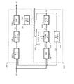
도 2는 본 발명의 일 실시예에 의한 신호 수신 장치의 블록도이다.
본 발명의 일 실시예에 의한 신호 수신 장치는 수신된 변조 신호(S1)에서 캐리어 신호(S2)를 복구하는 캐리어 복구부(100)와 변조 신호(S1)와 캐리어 신호(S2)를 이용하여 디지털 신호(S3)를 출력하는 디지털 신호 생성부(200)를 포함한다.
본 실시예에서 캐리어 복구부(100)는 아날로그 방식의 위상 고정 루프(Phase Locked Loop)의 구성을 포함한다.
캐리어 복구부(100)는 변조 신호(S1)와 제 1 분주 신호(S21)의 주파수 및 위상을 비교하는 제 1 PFD(110), 제 1 PFD(110)에서 출력된 신호에 따라 제 1 펌핑 전압(Vp1)을 조정하는 제 11 전하 펌프(121), 제 1 펌핑 전압(Vp1)을 필터링하여 제어 전압(Vc)을 출력하는 필터(150), 제어 전압(Vc)에 따라 캐리어 신호(S2)를 출력하는 발진기(130), 캐리어 신호(S2)를 분주하여 제 1 분주 신호(S21)를 출력하는 제 1 분주기(140)를 포함한다.
캐리어 복구부(100)는 디지털 신호(S3)에 따라 제 1 펌핑 전압(Vp1)을 조정하는 피드백 제어부(160)를 더 포함한다.
피드백 제어부(160)는 디지털 신호(S3)에 따라 피드백 신호(FB)를 출력하는 피드백 신호 생성부(170), 피드백 신호(FB)에 따라 제 1 펌핑 전압(Vp1)을 조정하는 제 12 전하 펌프(122)를 포함한다.
발진기(130), 제 1 분주기(140)는 종래에 알려진 구성 요소들로 구현될 수 있으므로 이에 대한 구체적인 설명은 생략한다.
본 실시예에서 디지털 신호 생성부(200)는 TDC(Time to Digital Converter)의 기능을 수행한다. 디지털 신호 생성부(200)는 캐리어 신호(S2)와 변조 신호(S1)의 위상차를 기준으로 디지털 신호(S3)를 생성한다.
디지털 신호 생성부(200)는 변조 신호(S1)와 제 1 분주 신호(S21)의 주파수 및 위상차를 탐지하는 제 2 PFD(210), 제 2 PFD(210)의 출력에 따라 제 2 펌핑 전압(Vp2)을 생성하는 제 2 전하 펌프(220), 제 2 펌핑 전압(Vp2)을 디지털 신호(S3)로 변환하는 ADC(Analog to Digital Converter, 230)를 포함한다.
디지털 신호 생성부(200)는 제 1 분주 신호(S21)를 기준으로 변조 신호(S1)의 위상차를 탐지하고 이에 대응하는 제 2 펌핑 전압(Vp2)을 생성하여 이를 디지털 신호(S3)로 변환함으로써 변조 신호(S1)의 위상에 대응하는 디지털 신호(S3)를 출력한다.
디지털 신호 생성부(200)는 캐리어 신호(S2)를 분주하여 제 2 분주 신호(S22)를 출력하는 제 2 분주기(240)를 더 포함한다. ADC(230)는 제 2 분주 신호(S21)에 동기하여 디지털 신호(S3)를 출력한다.
이에 따라 제 2 전하 펌프(220)는 제 2 분주 신호(S22)의 어느 한 주기 동안 제 2 펌핑 전압(Vp2)을 생성하고 이에 대응하는 디지털 신호(S3)는 제 2 분주 신호(S22)의 다음 주기에 출력된다.
제 1 분주기(140)와 제 2 분주기(240)의 분주율은 실시예에 따라 다양하게 결정될 수 있다. 본 실시예에서 제 2 분주 신호(S22)의 주기는 제 1 분주 신호(S21)의 주기와 같거나 제 1 분주 신호(S21)의 주기의 배수가 되도록 선택될 수 있다.
도 3은 도 2의 제 1 PFD(110)의 회로도이다.
제 1 PFD(110)는 캐리어 신호(S1)에 따라 제 1 펌핑 신호(UP)를 출력하는 제 1 플립플롭(111), 제 1 분주 신호(S21)에 따라 제 2 펌핑 신호(DN)를 출력하는 제 2 플립플롭(112), 제 1 펌핑 신호(UP)와 제 2 펌핑 신호(DN)이 모두 활성화된 경우 제 1 플립플롭(111)과 제 2 플립플롭(112)을 리셋하는 낸드 게이트(113)를 포함한다.
본 실시예에서 제 1 펌핑 신호(UP)는 변조 신호(S1)의 위상이 제 1 분주 신호(S21)의 위상보다 앞서는 구간 동안 하이 레벨을 갖는 펄스 형태를 가지고 제 2 펌핑 신호(DN)는 제 1 분주 신호(S21)의 위상이 변조 신호(S1)의 위상보다 앞서는 구간 동안 하이 레벨을 갖는 펄스 형태를 가진다.
제 2 PFD(210)는 신호의 종류를 제외하고 제 1 PFD(110)와 실질적으로 동일하게 구성될 수 있다.
도 3에 도시된 회로도는 제 1 PFD(210) 또는 제 2 PFD(220)를 구현하는 일 예로서 다른 실시예에서는 다른 구조의 회로를 사용할 수 있다.
도 4는 제 11 전하 펌프(121), 제 12 전하 펌프(122) 및 필터(150)의 회로도이다.
먼저 필터(150)는 로우패스 필터로서 저항(151)과 캐패시터(152)를 이용하여 구현할 수 있다. 도시된 예는 간단한 형태의 로우패스 필터를 예시한 것으로서 다른 실시예에서는 다른 구조의 필터를 사용할 수 있다.
본 실시예에서 제 11 전하 펌프(121)는 전원 전압과 접지 전압 사이에 직렬로 연결된 제 11 PMOS 트랜지스터(P11), 제 12 PMOS 트랜지스터(P12), 제 11 NMOS 트랜지스터(N11), 제 12 NMOS 트랜지스터(N12)를 포함한다.
제 12 PMOS 트랜지스터(P12)와 제 11 NMOS 트랜지스터(N11)의 공통 드레인은 필터(150)의 입력단과 연결된다.
제 11 PMOS 트랜지스터(P11)의 게이트에는 제 1 바이어스 전압(VBP)이 입력되고 제 12 NMOS 트랜지스터(N12)의 게이트에는 제 2 바이어스 전압(VBN)이 입력된다.
제 12 PMOS 트랜지스터(P12)의 게이트에는 제 1 펌핑 신호(UP)를 반전한 신호(/UP)가 입력되고, 제 11 NMOS 트랜지스터(N11)의 게이트에는 제 2 펌핑 신호(DN)가 입력된다.
제 1 펌핑 신호(UP)가 하이 레벨이 되는 구간에서 캐패시터(152)는 더 높은 전압으로 충전되고 제 2 펌핑 신호(DN)가 하이 레벨이 되는 구간에서 캐패시터(152)는 더 낮은 전압으로 방전된다.
본 실시예에서 제 12 전하 펌프(122)는 전원 전압과 접지 전압 사이에 직렬로 연결된 제 21 PMOS 트랜지스터(P21), 제 22 PMOS 트랜지스터(P22), 제 21 NMOS 트랜지스터(N21), 제 22 NMOS 트랜지스터(N22)를 포함한다.
제 22 PMOS 트랜지스터(P22)와 제 21 NMOS 트랜지스터(N21)의 공통 드레인은 필터(150)의 입력단과 연결된다.
제 21 PMOS 트랜지스터(P21)의 게이트에는 제 1 바이어스 전압(VBP)이 입력되고 제 22 NMOS 트랜지스터(N22)의 게이트에는 제 2 바이어스 전압(VBN)이 입력된다.
제 22 PMOS 트랜지스터(P22)의 게이트에는 제 1 피드백 신호(FBUP)를 반전한 신호(/FBUP)가 입력되고, 제 21 NMOS 트랜지스터(N21)의 게이트에는 제 2 피드백 신호(FBDN)가 입력된다.
이에 따라 제 1 피드백 신호(FBUP)가 하이 레벨이 되는 구간에서 캐패시터(152)는 더 높은 전압으로 충전되고 제 2 피드백 신호(DN)가 하이 레벨이 되는 구간에서 캐패시터(152)는 더 낮은 전압으로 방전된다.
제 22 전하 펌프(122)에 입력되는 제 1 피드백 신호(FBUP)와 제 2 피드백 신호(FBDN)는 피드백 신호 생성부(170)에서 출력되는 피드백 신호(FB)에 대응한다.
도 5는 피드백 신호 생성부(170)의 세부 블록도이다.
피드백 신호 생성부(170)는 덧셈부(171), 누적기(172), 비교부(173), 곱셈부(174, 175), 플립플롭(176)을 포함한다.
누적기(172)와 플립플롭(176)은 제 1 분주 신호(S21)에 동기하여 동작한다.
비교부(173)는 누적기(172)에서 출력된 누적기 신호(S32)와 임계점(α)을 비교하여 제 1 신호(S33)와 제 2 신호(S34)를 출력한다.
예를 들어 누적기 신호(S32)의 절대값이 임계점(α)보다 작으면 제 1 신호(S33) 및 제 2 신호(S34)는 모두 0이 된다.
누적기 신호(S32)가 양이고 절대값이 임계점(α)이상이면 제 1 신호(S33)는 1이고 제 2 신호(S34)는 0이 된다.
누적기 신호(S32)가 음이고 절대값이 임계점(α)이상이면 제 1 신호(S33)는 0이고 제 2 신호(S34)는 1이 된다.
플립플롭(176)은 제 1 분주 신호(S21)에 동기하여 제 1 신호(S33)를 래치하여 제 1 피드백 신호(FBUP)를 출력하고 제 2 신호(S34)를 래치하여 제 2 피드백 신호(FBDN)를 출력한다.
덧셈부(171)는 디지털 신호(S3)와 제 2 신호(S34)에 임계점(α)을 곱한 제 2 곱셈 신호(S36)를 더하고 제 1 신호(S33)에 임계점(α)을 곱한 제 1 곱셈 신호(S35)를 뺀 최종 덧셈 신호(S31)을 누적기(172)에 제공한다.
누적기(172)는 제 1 분주 신호(S21)에 동기하여 덧셈 신호(S31)의 값과 기존에 저장된 값을 더하여 저장된 값을 갱신한다.
도 6은 피드백 신호 생성부(170)의 동작을 설명하는 파형도이다.
(A)는 제 1 분주 신호(S21)와 제 2 분주 신호(S22)의 주기가 동일한 경우이고 (B)는 제 2 분주 신호(S22)의 주기가 제 1 분주 신호(S21)의 주기의 두 배인 경우이다. 이하에서 임계점(α)은 16보다 큰 양수로 가정한다.
먼저 (A)의 경우를 설명한다.
T0에서 디지털 신호(S3)의 값은 4로 출력되고, 누적기(172)는 T0에서 α-6을 저장하는 것으로 가정한다. 누적기 신호(S32)가 α-6이며 그 절대값은 임계점보다 작으므로 제 1 신호(S33) 및 제 2 신호(S34)는 0이 되고, 제 1 곱셈 신호(S35) 및 제 2 곱셈 신호(S36)는 0이 된다. 이에 따라 덧셈 신호(S31)는 4가 된다.
T1에서 디지털 신호(S3)의 값은 7인 것으로 가정한다. 누적기 신호(S32)는 기존 값인 α-6에 4를 더한 α-2가 된다. 누적기 신호(S32)의 절대값은 임계점보다 작으므로 제 1 신호(S33) 및 제 2 신호(S34)는 0이 되고 제 1 곱셈 신호(S35) 및 제 2 곱셈 신호(S36)는 0이 된다. 이에 따라 덧셈 신호(S31)는 7이 된다. 또한 플립플롭(176)은 제 1 신호(S33) 및 제 2 신호(S34)를 래치하여 제 1 피드백 신호(FBUP) 및 제 2 피드백 신호(FBDN)는 0이 된다.
T2에서 디지털 신호(S3)의 값은 -6인 것으로 가정한다. 누적기 신호(S32)는 기존 값인 α-2에 7을 더한 α+5가 된다. 누적기 신호(S32)의 절대값은 임계점보다 크고 부호는 양이므로 제 1 신호(S33)는 1, 제 2 신호(S34)는 0이 되고 제 1 곱셈 신호(S35)는 α, 제 2 곱셈 신호(S36)는 0이 된다. 이에 따라 덧셈 신호(S31)는 -α-6이 된다. 또한 플립플롭(176)은 제 1 신호(S33) 및 제 2 신호(S34)를 래치하여 제 1 피드백 신호(FBUP) 및 제 2 피드백 신호(FBDN)는 0이 된다.
T3에서 누적기 신호(S32)는 기존 값인 α+5에 -α-6을 더한 -1이 된다. 누적기 신호(S32)의 절대값은 임계점보다 작으므로 제 1 신호(S33)는 0, 제 2 신호(S34)는 0이 되고 제 1 곱셈 신호(S35)는 0, 제 2 곱셈 신호(S36)는 0이 된다. 또한 플립플롭(176)은 제 1 신호(S33) 및 제 2 신호(S34)를 래치하여 제 1 피드백 신호(FBUP)는 0, 제 2 피드백 신호(FBDN)는 1이 된다.
T4에서 누적기 신호(S32)는 기존 값인 α+5에 -α-5을 더한 -1이 된다. 누적기 신호(S32)의 절대값은 임계점보다 작으므로 제 1 신호(S33)는 0, 제 2 신호(S34)는 0이 되고 제 1 곱셈 신호(S35)는 0, 제 2 곱셈 신호(S36)는 0이 된다. 또한 플립플롭(176)은 제 1 신호(S33) 및 제 2 신호(S34)를 래치하여 제 1 피드백 신호(FBUP)는 0, 제 2 피드백 신호(FBDN)는 0이 된다.
다음으로 (B)의 경우를 설명한다.
(B)의 경우는 제 2 분주 신호(S22)의 주기가 제 1 분주 신호(S21)의 주기의 2배가 되므로 디지털 신호(S3)가 변하는 주기가 제 1 분주 신호(S21)의 두 배가 되는 점에서 (A)의 경우와 상이하다.
T5에서 디지털 신호(S3)의 값은 -4로 출력되고, 누적기(612)는 T5에서 -α+6을 저장하는 것으로 가정한다. 누적기 신호(S32)가 -α+6이며 그 절대값은 임계점보다 작으므로 제 1 신호(S33) 및 제 2 신호(S34)는 0이 되고, 제 1 곱셈 신호(S35) 및 제 2 곱셈 신호(S36)는 0이 된다. 이에 따라 덧셈 신호(S31)는 -4가 된다.
T6에서 디지털 신호(S3)의 값은 -4로 동일하다. 누적기 신호(S32)는 기존 값인 -α+6에 -4를 더한 -α+2가 된다. 누적기 신호(S32)의 절대값은 임계점보다 작으므로 제 1 신호(S33) 및 제 2 신호(S34)는 0이 되고 제 1 곱셈 신호(S35) 및 제 2 곱셈 신호(S36)는 0이 된다. 이에 따라 덧셈 신호(S31)는 -4가 된다. 또한 플립플롭(176)은 제 1 신호(S33) 및 제 2 신호(S34)를 래치하여 제 1 피드백 신호(FBUP) 및 제 2 피드백 신호(FBDN)는 0이 된다.
T7에서 디지털 신호(S3)의 값은 -7인 것으로 가정한다. 누적기 신호(S32)는 기존 값인 -α+2에 -4를 더한 -α-2가 된다. 누적기 신호(S32)의 절대값은 임계점보다 크고 부호는 음이므로 제 1 신호(S33)는 0, 제 2 신호(S34)는 1이 되고 제 1 곱셈 신호(S35)는 0, 제 2 곱셈 신호(S36)는 α이 된다. 이에 따라 덧셈 신호(S31)는 α-7이 된다. 또한 플립플롭(176)은 제 1 신호(S33) 및 제 2 신호(S34)를 래치하여 제 1 피드백 신호(FBUP) 및 제 2 피드백 신호(FBDN)는 0이 된다.
T8에서 누적기 신호(S32)는 기존 값인 -α-2에 α-7을 더한 -9가 된다. 누적기 신호(S32)의 절대값은 임계점보다 작으므로 제 1 신호(S33)는 0, 제 2 신호(S34)는 0이 되고 제 1 곱셈 신호(S35)는 0, 제 2 곱셈 신호(S36)는 0이 된다. 또한 플립플롭(176)은 제 1 신호(S33) 및 제 2 신호(S34)를 래치하여 제 1 피드백 신호(FBUP)는 1, 제 2 피드백 신호(FBDN)는 0이 된다.
T9에서 디지털 신호(S3)의 값은 6인 것으로 가정한다. 누적기 신호(S32)는 기존 값인 -9에 -7를 더한 -16이 된다. 누적기 신호(S32)의 절대값은 임계점보다 작으므로 제 1 신호(S33)는 0, 제 2 신호(S34)는 0이 되고 제 1 곱셈 신호(S35)는 0, 제 2 곱셈 신호(S36)는 0이 된다. 이에 따라 덧셈 신호(S31)는 6이 된다. 또한 플립플롭(176)은 제 1 신호(S33) 및 제 2 신호(S34)를 래치하여 제 1 피드백 신호(FBUP) 및 제 2 피드백 신호(FBDN)는 0이 된다.
(A)의 경우에는 누적기(172)의 값이 양의 방향으로 증가하고 (B)의 경우에는 누적기(172)의 값이 음의 방향으로 증가하였다.
누적기(172)의 값이 양 또는 음의 방향으로 증가하는 경우 캐리어 신호(S2)의 위상 역시 해당 방향으로 변할 가능성이 높아진다.
피드백 신호 생성부(170)는 누적기(172)의 절대값이 임계점을 초과하여 양의 방향으로 증가하는 시점에서 누적기(172)의 값을 임계점의 크기만큼 줄이고 제 2 피드백 신호(FBDN)를 활성화한다. 이에 따라 도 4의 제 21 NMOS 트랜지스터(N21)가 켜지고 제어 전압(Vc)이 증가하여 누적기(172)의 값의 변화가 커지는 것을 억제한다.
또한 피드백 신호 생성부(170)는 누적기(172)의 절대값이 임계점을 초과하여 음의 방향으로 증가하는 시점에서 누적기(172)의 값을 임계점의 크기만큼 증가시키고 제 1 피드백 신호(FBUP)를 활성화한다. 이에 따라 도 4의 제 22 PMOS 트랜지스터(N22)가 켜지고 제어 전압(Vc)을 감소시켜 누적기(172)의 값의 변화가 커지는 것을 억제한다.
도 7은 종래의 경우와 본 발명의 경우 제어 전압(Vc)의 변동을 비교하여 나타낸 그래프이다.
실선은 종래 기술의 경우로서 로킹 직후의 제어 전압(Vl)을 기준으로 위상차가 가장 큰 신호가 연속하여 발생되는 경우를 상한과 하한으로 하면서 제어 전압(Vc)의 변동 가능한 폭은 시간에 따라 증가한다.
종래의 기술에서 제어 전압(Vc)의 큰 변동을 억제하기 위하여 로우패스 필터(15)는 대용량의 캐패시터를 필요로 한다.
본 발명의 일 실시예에서는 피드백 제어부(160)의 제어에 의해 제어 전압(Vc)의 변동폭(2Vd)이 종래의 기술에 비하여 제한된다. 이때 변동폭(2Vd)은 임계점(α)의 값에 따라 달라질 수 있다.
본 발명의 일 실시예에서는 종래에 비하여 상대적으로 작은 변동폭(2Vd)을 억제할 수 있을 정도의 작은 용량을 갖는 캐패시터(152)로 충분하다. 이에 따라 본 발명의 일 실시예에서는 캐패시터(152)로 인한 회로 면적의 증가 문제가 크지 않다.
도 8은 본 발명의 다른 실시예에 의한 신호 수신 장치의 블록도이다.
도 2의 실시예에서 제 1 PFD(110)와 제 2 PFD(210)는 실질적으로 동일한 구성요소들을 포함할 수 있다.
도 8의 실시예는 이러한 점에 착안한 것으로서 도 2에서 제 2 PFD(210)를 포함하지 않고 캐리어 복구부(100)의 제 11 전하 펌프(121)와 디지털 신호 생성부(200)의 제 2 전하 펌프(220)가 제 1 PFD(110)의 출력을 공통적으로 입력받는다.
도 8에서는 제 1 PFD(110)가 캐리어 복구부(100)와 디지털 신호 생성부(200)의 외부에 위치하는 것으로 도시하였다. 그러나 통상의 기술자는 도 8을 참조하여 제 1 PFD(110)가 캐리어 복구부(100) 또는 디지털 신호 생성부(200) 내에 포함되는 실시예에 대해서도 용이하게 알 수 있으며 이러한 변형은 실질적으로 도 8과 균등한 관계에 있다.
도 8에서 다른 구성 요소들은 도 2 내지 도 7을 참조하여 개시한 바와 실질적으로 동일하므로 구체적인 설명은 생략한다.
도 9는 본 발명의 다른 실시예에 의한 신호 수신 장치의 블록도이다.
캐리어 복구부(1000)는 디지털 방식의 위상 고정 루프의 구성을 포함한다. 디지털 신호 생성부(200)의 구성은 전술한 바와 실질적으로 동일하므로 구체적인 설명을 생략한다.
본 실시예에서 캐리어 복구부(1000)는 변조 신호(S1)와 제 1 분주 신호(S21)의 주파수 및 위상을 비교하는 TDC(1100), TDC(1100)에서 출력된 비교 코드(TDCC)와 피드백 코드(FC) 따라 제어 코드(CC)를 출력하는 디지털 필터(1200), 제어 코드(CC)에 따라 캐리어 신호(S2)를 출력하는 디지털 발진기(1300), 캐리어 신호(S2)를 분주하여 제 1 분주 신호(S21)를 출력하는 제 1 분주기(1400)를 포함한다.
캐리어 복구부(1000)는 디지털 신호(S3)에 따라 피드백 코드(FC)를 출력하는 피드백 제어부(1600)를 더 포함한다.
TDC(1100), 디지털 발진기(1300), 제 1 분주기(1400)는 종래에 알려진 다양한 구현 예들이 있으므로 이에 대한 구체적인 설명은 생략한다.
도 10은 도 9의 피드백 제어부(1600)와 디지털 필터(1200)의 세부 블록도이다.
도 10의 디지털 필터(1200)는 곱셈부(1220, 1230), 덧셈부(1210, 1240, 1250) 및 누적기(1260)를 포함하는 일반적인 디지털 필터의 구성을 예시한다. 디지털 필터(1200)는 실시예에 따라서 다양한 방식으로 구현될 수 있다.
디지털 필터(1200)는 덧셈부(1210)에서 피드백 코드(FC)와 비교 코드(TDCC)를 입력받아 제어 코드(CC)를 생성한다.
피드백 제어부(1600)는 디지털 신호(S3)에 상수(c)를 곱하여 피드백 코드(FC)를 출력하는 곱셈부(1610)를 포함한다.
본 실시예에서 상수(c)의 크기는 ADC(230)의 해상도와 TDC(1100)의 해상도의 비로 정해질 수 있다.
ADC(230)의 해상도는 디지털 신호(S3)의 값 1에 대응하는 위상차를 의미하고 TDC(1100)의 해상도는 비교 코드(TDCC)의 값 1에 대응하는 위상차를 의미한다.
예를 들어 ADC(230)의 해상도가 4도이고 TDC(1100)의 해상도가 4도로 동일하면 상수(c)의 크기는 1로 정해질 수 있다. 다른 예에서 ADC(230)의 해상도가 4도이고 TDC(1100)의 해상도가 8도이면 상수(c)의 크기는 0.5로 정해질 수 있다.
본 실시예에서 덧셈부(1210)는 비교 코드(TDCC)에서 피드백 코드(FC)를 뺀 값을 출력하여 필터링이 수행되도록 함으로써 디지털 신호(S3)의 변화에 의한 캐리어 신호(S2)의 위상 변화를 억제하는 방향으로 피드백 코드(FC)가 생성될 수 있다.
이에 따라 디지털 발진기(1300)에서 출력되는 캐리어 신호(S2)는 디지털 신호(S3)의 값이 변하더라도 본래의 위상을 유지하게 된다.
디지털 방식의 캐리어 복구부(1000)는 캐리어 신호(S2)의 주파수가 높더라도 실시간 피드백이 가능한 점에서 피드백에 시간이 지연되는 아날로그 방식의 캐리어 복구부(100)에 비하여 유리할 수 있다. 또한 디지털 방식의 캐리어 복구부(1000)는 캐패시터를 사용하지 않아도 되므로 아날로그 방식의 캐리어 복구부(100)에 비하여 회로의 면적을 줄이는데 보다 유리할 수 있다.
이상에서 도면을 참조하여 본 발명의 실시예를 개시하였다. 이상의 개시는 설명을 위한 것으로서 본 발명의 권리범위를 한정하는 것은 아니며, 본 발명의 권리범위는 이하의 특허청구범위에 문언적으로 기재된 범위와 그 균등범위에 의해 정해진다.
Claims (22)
- 변조 신호와 캐리어 신호의 주파수 또는 위상의 차이에 따라 가변하는 디지털 신호를 생성하는 디지털 신호 생성부; 및상기 변조 신호로부터 상기 캐리어 신호를 복구하되 상기 디지털 신호에 따라 상기 캐리어 신호의 위상 변화를 제어하는 피드백 제어부를 포함하는 캐리어 복구부를 포함하는 신호 수신 장치.
- 청구항 1에 있어서, 상기 캐리어 복구부는 상기 캐리어 신호와 동일한 주기를 갖거나 상기 캐리어 신호를 분주한 신호인 제 1 분주 신호와 상기 변조 신호의 위상 또는 주파수 차이에 대응하여 생성되는 제어 전압에 따라 상기 캐리어 신호를 출력하는 발진기를 더 포함하되, 상기 피드백 제어부는 상기 디지털 신호에 따라 상기 제어 전압을 조절하는 신호 수신 장치.
- 청구항 2에 있어서, 상기 피드백 제어부는 상기 디지털 신호의 누적값을 임계점과 비교한 결과에 따라 상기 제어 전압을 조절하는 신호 수신 장치.
- 청구항 3에 있어서, 상기 피드백 제어부는 상기 디지털 신호의 누적값이 임계점을 초과하는 경우 상기 누적값의 절대값을 감소시키고 상기 제어 전압을 조절하는 신호 수신 장치.
- 청구항 2에 있어서, 상기 캐리어 복구부는 상기 제 1 분주 신호와 상기 변조 신호의 위상 또는 주파수를 비교하는 제 1 위상 주파수 비교부;상기 제 1 위상 주파수 비교부의 출력에 따라 출력 전압을 증가 또는 감소시키는 제 11 전압 펌프;상기 제 11 전압 펌프의 출력을 필터링하여 상기 제어 전압을 출력하는 필터; 및상기 제어 전압에 따라 상기 캐리어 신호를 출력하는 발진기를 더 포함하는 신호 수신 장치.
- 청구항 5에 있어서, 상기 캐리어 복구부는 상기 캐리어 신호를 분주하여 상기 제 1 분주 신호를 출력하는 제 1 분주기를 더 포함하는 신호 수신 장치.
- 청구항 5에 있어서, 상기 피드백 제어부는 상기 디지털 신호 및 상기 제 1 분주 신호에 따라 피드백 신호를 생성하는 피드백 신호 생성부 및상기 피드백 신호에 따라 출력 전압을 증가 또는 감소시키는 제 12 전압 펌프를 포함하되, 상기 제 12 전압 펌프의 출력단은 상기 제 11 전압 펌프의 출력단과 공통 연결되는 신호 수신 장치.
- 청구항 7에 있어서, 상기 피드백 신호 생성부는 상기 제 1 분주 신호에 동기하여 상기 디지털 신호를 누적하여 저장한 누적값과 임계점을 비교하여 상기 제 12 전압 펌프의 출력을 증가시키는 제 1 피드백 신호와 상기 제 12 전압 펌프의 출력을 감소시키는 제 2 피드백 신호를 출력하는 신호 수신 장치.
- 청구항 8에 있어서, 상기 피드백 신호 생성부는 상기 누적값의 절대값이 상기 임계점 미만이면 상기 제 1 피드백 신호와 제 2 피드백 신호를 비활성화하고 상기 누적값의 절대값이 임계점 이상이면 상기 누적값의 절대값을 감소시키고 상기 제 1 피드백 신호 또는 제 2 피드백 신호 중 어느 하나를 활성화시키는 신호 수신 장치.
- 청구항 9에 있어서, 상기 피드백 신호 생성부는제 2 신호가 활성화되는 경우 상기 디지털 신호와 상기 임계점을 더하고, 제 1 신호가 활성화되는 경우 상기 디지털 신호와 상기 임계점을 더하는 덧셈기;상기 제 1 분주 신호에 동기하여 상기 덧셈기의 출력을 누적하여 저장하는 누적기;상기 누적기에서 출력되는 상기 누적값을 상기 임계점과 비교하여 상기 제 1 신호 또는 상기 제 2 신호 중 어느 하나를 활성화하는 비교기;상기 제 1 분주 신호에 따라 상기 제 1 신호를 래치하여 상기 제 1 피드백 신호를 출력하고 상기 제 2 신호를 래치하여 상기 제 2 피드백 신호를 출력하는 플립플롭을 포함하는 신호 수신 장치.
- 청구항 2에 있어서, 상기 디지털 신호 생성부는 상기 캐리어 신호와 동일한 주기를 갖거나 상기 캐리어 신호를 분주한 신호인 제 2 분주 신호에 동기하여 상기 제 1 분주 신호와 상기 변조 신호의 위상 또는 주파수 차이에 따라 생성되는 상기 디지털 신호를 출력하는 신호 수신 장치.
- 청구항 11에 있어서, 상기 제 2 분주 신호의 주기는 상기 제 1 분주 신호의 주기의 배수인 신호 수신 장치.
- 청구항 11에 있어서, 상기 디지털 신호 생성부는상기 제 1 분주 신호와 상기 변조 신호의 위상 또는 주파수 차이를 탐지하는 제 2 위상 주파수 비교부;상기 제 2 위상 주파수 비교부의 출력에 따라 제 2 제어 전압을 출력하는 제 2 전하 펌프; 및상기 제 2 제어 전압을 디지털로 변환하되 상기 제 2 분주 신호에 동기하여 변환된 디지털 값을 상기 디지털 신호로 출력하는 아날로그 디지털 변환부를 포함하는 신호 수신 장치.
- 청구항 5에 있어서, 상기 디지털 신호 생성부는상기 제 1 위상 주파수 비교부의 출력에 따라 제 2 제어 전압을 출력하는 제 2 전하 펌프; 및상기 제 2 제어 전압을 디지털로 변환하되 제 2 분주 신호에 동기하여 변환된 디지털 값을 상기 디지털 신호로 출력하는 아날로그 디지털 변환부를 포함하되,상기 제 2 분주 신호는 상기 캐리어 신호와 동일한 주기를 갖거나 상기 캐리어 신호를 분주한 신호인 신호 수신 장치.
- 청구항 1에 있어서, 상기 캐리어 복구부는 상기 캐리어 신호와 동일한 주기를 갖거나 상기 캐리어 신호를 분주한 신호인 제 1 분주 신호와 상기 변조 신호의 위상 또는 주파수 차이에 대응하여 생성되는 제어 코드에 따라 상기 캐리어 신호를 출력하는 디지털 발진기를 포함하되, 상기 피드백 제어부는 상기 디지털 신호에 따라 상기 제어 코드의 값을 변경시키는 신호 수신 장치.
- 청구항 15에 있어서, 상기 캐리어 복구부는 상기 변조 신호와 상기 제 1 분주 신호의 위상 또는 주파수 차이에 대응하는 비교 코드를 출력하는 위상 주파수 탐지기; 및상기 비교 코드와 피드백 코드를 필터링하여 상기 제어 코드를 출력하는 디지털 필터를 더 포함하는 신호 수신 장치.
- 청구항 16에 있어서, 상기 캐리어 신호를 분주하여 상기 제 1 분주 신호를 출력하는 제 1 분주기를 더 포함하는 신호 수신 장치.
- 청구항 16에 있어서, 상기 디지털 필터는 상기 피드백 코드와 상기 비교 코드를 더한 값을 필터링하는 신호 수신 장치.
- 청구항 18에 있어서, 상기 디지털 신호 생성부는 상기 캐리어 신호와 동일한 주기를 갖거나 상기 캐리어 신호를 분주한 신호인 제 2 분주 신호에 동기하여 상기 제 1 분주 신호와 상기 변조 신호의 위상 또는 주파수 차이에 대응하여 정해지는 상기 디지털 신호를 출력하는 신호 수신 장치.
- 청구항 19에 있어서, 상기 디지털 신호 생성부는 상기 제 1 분주 신호와 상기 변조 신호의 위상 또는 주파수 차이에 대응하여 생성되는 전압을 디지털로 변환하고 상기 제 2 분주 신호에 동기하여 상기 디지털 신호로 출력하는 아날로그 디지털 컨버터를 포함하는 신호 수신 장치.
- 청구항 20에 있어서, 상기 피드백 제어부는 상기 디지털 신호에 상수를 곱하여 상기 피드백 코드로 출력하는 신호 수신 장치.
- 청구항 21에 있어서, 상기 상수의 크기는 상기 위상 주파수 탐지기의 해상도와 상기 아날로그 디지털 컨버터의 해상도의 비로 결정되는 신호 수신 장치.
Applications Claiming Priority (2)
| Application Number | Priority Date | Filing Date | Title |
|---|---|---|---|
| KR10-2015-0031696 | 2015-03-06 | ||
| KR1020150031696A KR101595077B1 (ko) | 2015-03-06 | 2015-03-06 | 신호 수신 장치 |
Publications (1)
| Publication Number | Publication Date |
|---|---|
| WO2016144024A1 true WO2016144024A1 (ko) | 2016-09-15 |
Family
ID=55447569
Family Applications (1)
| Application Number | Title | Priority Date | Filing Date |
|---|---|---|---|
| PCT/KR2016/001860 Ceased WO2016144024A1 (ko) | 2015-03-06 | 2016-02-25 | 신호 수신 장치 |
Country Status (2)
| Country | Link |
|---|---|
| KR (1) | KR101595077B1 (ko) |
| WO (1) | WO2016144024A1 (ko) |
Citations (4)
| Publication number | Priority date | Publication date | Assignee | Title |
|---|---|---|---|---|
| JP2009027581A (ja) * | 2007-07-23 | 2009-02-05 | Renesas Technology Corp | 半導体集積回路 |
| KR20090063641A (ko) * | 2007-12-14 | 2009-06-18 | 한양대학교 산학협력단 | 저온 폴리-실리콘 공정에 적합한 디지털 위상 고정 루프 |
| US8705663B2 (en) * | 2012-01-31 | 2014-04-22 | Innophase Inc. | Receiver architecture and methods for demodulating binary phase shift keying signals |
| US8773182B1 (en) * | 2013-02-01 | 2014-07-08 | Intel Corporation | Stochastic beating time-to-digital converter (TDC) |
Family Cites Families (3)
| Publication number | Priority date | Publication date | Assignee | Title |
|---|---|---|---|---|
| JP3137370B2 (ja) | 1991-08-07 | 2001-02-19 | 株式会社東芝 | デジタルpll回路 |
| US5966416A (en) | 1996-11-21 | 1999-10-12 | Dsp Group, Inc. | Verification of PN synchronization in a spread-spectrum communications receiver |
| JP2002141962A (ja) | 2000-11-01 | 2002-05-17 | Mitsubishi Electric Corp | キャリア再生回路およびロック検出回路 |
-
2015
- 2015-03-06 KR KR1020150031696A patent/KR101595077B1/ko active Active
-
2016
- 2016-02-25 WO PCT/KR2016/001860 patent/WO2016144024A1/ko not_active Ceased
Patent Citations (4)
| Publication number | Priority date | Publication date | Assignee | Title |
|---|---|---|---|---|
| JP2009027581A (ja) * | 2007-07-23 | 2009-02-05 | Renesas Technology Corp | 半導体集積回路 |
| KR20090063641A (ko) * | 2007-12-14 | 2009-06-18 | 한양대학교 산학협력단 | 저온 폴리-실리콘 공정에 적합한 디지털 위상 고정 루프 |
| US8705663B2 (en) * | 2012-01-31 | 2014-04-22 | Innophase Inc. | Receiver architecture and methods for demodulating binary phase shift keying signals |
| US8773182B1 (en) * | 2013-02-01 | 2014-07-08 | Intel Corporation | Stochastic beating time-to-digital converter (TDC) |
Non-Patent Citations (1)
| Title |
|---|
| VAN DE BEEK, R.C.H. ET AL.: "A 13.56Mbps PSK Receiver for 13.56MHz RFID Applications", 2012 IEEE RADIO FREQUENCY INTEGRATED CIRCUITS SYMPOSIUM, June 2012 (2012-06-01), pages 239 - 242, XP032203345, Retrieved from the Internet <URL:http://ieeexplore.ieee.org/stamp/stamp.jsp?tp=&arnumber=6242272> * |
Also Published As
| Publication number | Publication date |
|---|---|
| KR101595077B1 (ko) | 2016-02-26 |
Similar Documents
| Publication | Publication Date | Title |
|---|---|---|
| US7629854B2 (en) | Switch-capacitor loop filter for phase lock loops | |
| KR950028348A (ko) | 클록 재생 회로 및 이 클록 재생 회로등에 사용되는 소자들 | |
| WO1993018579A1 (en) | Video signal data and composite synchronization extraction circuit for on-screen display | |
| JPH10126260A (ja) | 位相同期ループのロック検出装置 | |
| KR0138764B1 (ko) | 검출 시스템 | |
| WO2017065510A1 (ko) | 신호의 상승 에지와 하강 에지를 이용하여 높은 대역폭을 가지는 위상 동기 루프 | |
| US6429901B1 (en) | PLL circuit and phase lock detector | |
| TW201408065A (zh) | 影像感測器及其行類比數位轉換器 | |
| US7288976B2 (en) | Charge pump circuit and method thereof | |
| PL109075B1 (en) | Synchronizing system for television receivers | |
| WO2019172467A1 (en) | Phase-locked loop apparatus and method for clock synchronization | |
| WO2016144024A1 (ko) | 신호 수신 장치 | |
| KR100196618B1 (ko) | 텔레비젼 신호 검출회로 | |
| KR100287510B1 (ko) | 신호클램핑장치 | |
| CN101304477A (zh) | 分离视频信号中同步信号的装置与其方法 | |
| US4024343A (en) | Circuit arrangement for synchronizing an output signal in accordance with a periodic pulsatory input signal | |
| WO2013042918A1 (ko) | 복수 개의 램프 신호를 사용하는 다중 스텝 구조의 adc 및 이를 이용한 아날로그-디지털 변환 방법 | |
| WO2015056877A1 (ko) | 싱크의 송신 클럭 생성 장치 및 생성된 송신 클럭을 이용한 송신 방법 | |
| US3991270A (en) | Circuit arrangement for line synchronization in a television receiver | |
| US3727149A (en) | Burst control circuit having a voltage responsive oscillator | |
| US3418425A (en) | System for reducing low frequency variations in the average value of a signal | |
| US4891565A (en) | Field deflection circuit in a picture display device | |
| WO2016027945A1 (ko) | 복수의 부궤환 루프를 구비한 위상고정루프 장치 | |
| KR19980033965A (ko) | 광통신 수신기용 클럭 및 데이타(Data) 복구회로 | |
| KR100297854B1 (ko) | 위상 동기 루프의 발진기 제어용 d/a 변환기_ |
Legal Events
| Date | Code | Title | Description |
|---|---|---|---|
| 121 | Ep: the epo has been informed by wipo that ep was designated in this application |
Ref document number: 16761911 Country of ref document: EP Kind code of ref document: A1 |
|
| NENP | Non-entry into the national phase |
Ref country code: DE |
|
| 122 | Ep: pct application non-entry in european phase |
Ref document number: 16761911 Country of ref document: EP Kind code of ref document: A1 |