WO2016136374A1 - 光触媒構造体および光電池 - Google Patents
光触媒構造体および光電池 Download PDFInfo
- Publication number
- WO2016136374A1 WO2016136374A1 PCT/JP2016/052531 JP2016052531W WO2016136374A1 WO 2016136374 A1 WO2016136374 A1 WO 2016136374A1 JP 2016052531 W JP2016052531 W JP 2016052531W WO 2016136374 A1 WO2016136374 A1 WO 2016136374A1
- Authority
- WO
- WIPO (PCT)
- Prior art keywords
- light absorber
- nanorod
- nanorods
- structure according
- photocatalyst structure
- Prior art date
- Legal status (The legal status is an assumption and is not a legal conclusion. Google has not performed a legal analysis and makes no representation as to the accuracy of the status listed.)
- Ceased
Links
Images





Classifications
-
- B—PERFORMING OPERATIONS; TRANSPORTING
- B01—PHYSICAL OR CHEMICAL PROCESSES OR APPARATUS IN GENERAL
- B01J—CHEMICAL OR PHYSICAL PROCESSES, e.g. CATALYSIS OR COLLOID CHEMISTRY; THEIR RELEVANT APPARATUS
- B01J35/00—Catalysts, in general, characterised by their form or physical properties
- B01J35/30—Catalysts, in general, characterised by their form or physical properties characterised by their physical properties
-
- B—PERFORMING OPERATIONS; TRANSPORTING
- B01—PHYSICAL OR CHEMICAL PROCESSES OR APPARATUS IN GENERAL
- B01J—CHEMICAL OR PHYSICAL PROCESSES, e.g. CATALYSIS OR COLLOID CHEMISTRY; THEIR RELEVANT APPARATUS
- B01J27/00—Catalysts comprising the elements or compounds of halogens, sulfur, selenium, tellurium, phosphorus or nitrogen; Catalysts comprising carbon compounds
- B01J27/14—Phosphorus; Compounds thereof
- B01J27/186—Phosphorus; Compounds thereof with arsenic, antimony, bismuth, vanadium, niobium, tantalum, polonium, chromium, molybdenum, tungsten, manganese, technetium or rhenium
- B01J27/195—Phosphorus; Compounds thereof with arsenic, antimony, bismuth, vanadium, niobium, tantalum, polonium, chromium, molybdenum, tungsten, manganese, technetium or rhenium with vanadium, niobium or tantalum
- B01J27/198—Vanadium
- B01J27/199—Vanadium with chromium, molybdenum, tungsten or polonium
-
- C—CHEMISTRY; METALLURGY
- C01—INORGANIC CHEMISTRY
- C01B—NON-METALLIC ELEMENTS; COMPOUNDS THEREOF; METALLOIDS OR COMPOUNDS THEREOF NOT COVERED BY SUBCLASS C01C
- C01B3/00—Hydrogen; Gaseous mixtures containing hydrogen; Separation of hydrogen from mixtures containing it; Purification of hydrogen; Reversible storage of hydrogen
- C01B3/02—Production of hydrogen; Production of gaseous mixtures containing hydrogen
- C01B3/04—Production of hydrogen; Production of gaseous mixtures containing hydrogen by decomposition of inorganic compounds
-
- H—ELECTRICITY
- H01—ELECTRIC ELEMENTS
- H01G—CAPACITORS; CAPACITORS, RECTIFIERS, DETECTORS, SWITCHING DEVICES, LIGHT-SENSITIVE OR TEMPERATURE-SENSITIVE DEVICES OF THE ELECTROLYTIC TYPE
- H01G9/00—Electrolytic capacitors, rectifiers, detectors, switching devices, light-sensitive or temperature-sensitive devices; Processes of their manufacture
- H01G9/20—Light-sensitive devices
-
- Y—GENERAL TAGGING OF NEW TECHNOLOGICAL DEVELOPMENTS; GENERAL TAGGING OF CROSS-SECTIONAL TECHNOLOGIES SPANNING OVER SEVERAL SECTIONS OF THE IPC; TECHNICAL SUBJECTS COVERED BY FORMER USPC CROSS-REFERENCE ART COLLECTIONS [XRACs] AND DIGESTS
- Y02—TECHNOLOGIES OR APPLICATIONS FOR MITIGATION OR ADAPTATION AGAINST CLIMATE CHANGE
- Y02E—REDUCTION OF GREENHOUSE GAS [GHG] EMISSIONS, RELATED TO ENERGY GENERATION, TRANSMISSION OR DISTRIBUTION
- Y02E60/00—Enabling technologies; Technologies with a potential or indirect contribution to GHG emissions mitigation
- Y02E60/30—Hydrogen technology
- Y02E60/36—Hydrogen production from non-carbon containing sources, e.g. by water electrolysis
Definitions
- the present invention relates to a photocatalyst structure in which nanorod-like photocatalysts are arranged in an array, and more particularly to a photocatalyst structure excellent in water decomposition efficiency and a photovoltaic cell comprising the same as an anode.
- Hydrogen is a key raw material in the chemical industry and a clean energy source.
- Most of the conventional hydrogen production technologies are steam reforming technology (Non-patent document 1), coal gasification technology (Non-patent document 2), and biomass pyrolysis technology (non-patent document). It is based on the prior art such as literature 3).
- a fossil fuel is used, and a large amount of carbon dioxide (CO 2 ) is generated with the production of hydrogen (H 2 ).
- CO 2 carbon dioxide
- fossil fuels have a problem of resource depletion, and CO 2 emissions also have environmental problems such as global warming.
- the method of obtaining hydrogen by efficiently hydrolyzing solar energy using photocatalysis is considered one of the most attractive methods for producing clean and renewable fuels. Yes.
- fossil fuels are not used and CO 2 emissions are not generated. Therefore, it is attracting attention as a dreamy hydrogen production technology that is sustainable and clean.
- a typical PEC apparatus includes a semiconductor (photoanode) as a light absorber and a counter electrode made of a metal such as Pt, and these are immersed in an electrolytic aqueous solution.
- a semiconductor photoanode
- a counter electrode made of a metal such as Pt
- photons with an energy higher than the band gap of the photoanode are irradiated, electron-hole pairs are generated. Of these, holes are involved in the hydroxylation reaction at the interface between the photoanode and water.
- electrons move from the back contact of the photoanode through the external circuit to the Pt counter electrode. In this way, it contributes to the production of hydrogen using solar energy for water splitting.
- a photocatalytic material having a relatively small band gap of about 2 to 2.4 eV is required.
- a photocatalytic material having a relatively small band gap of about 2 to 2.4 eV.
- Examples of such a material include BiVO 4 , ⁇ - Examples thereof include Fe 2 O 3 and TaON.
- BiVO 4 bismuth vanadate
- STH Solar-to-Hydrogen efficiency
- AM1 air mass
- BiVO 4 is excellent in light absorption as described above, but has a high recombination rate between electrons and holes generated by light absorption, and the carrier diffusion length in the crystal is as short as about 70 nm, and its electrical conductivity is low. Therefore, there is a problem that the kinetics of water splitting due to recombination of electrons and holes generated by light irradiation is hindered. Although several attempts have been made to increase the electrical conductivity by doping BiVO 4 with Mo or W (Non-patent Documents 7 and 8), the results are not sufficient, and the low electrical conductivity of BiVO 4 Sexual issues still remain.
- ⁇ -Fe 2 O 3 is also a promising material, has a small band gap of about 2 eV, can absorb light in the range of about 40% of the solar spectrum, and has a theoretical energy efficiency of about 15%.
- the utilization efficiency of water in the visible light region for water decomposition is greatly limited due to low electron conductivity in the crystal and high recombination rate of electrons and holes. .
- An object of the present invention is to provide a photocatalyst structure excellent in water decomposition efficiency and a photovoltaic cell comprising the same as an anode by a combination of a photocatalyst having sufficiently high photoactivity even in the visible light region and a material excellent in electrical conductivity. It is in.
- a photocatalyst structure has a unit area ( ⁇ m) of a cylindrical nanorod having conductivity on a substrate having a conductive surface and having an average radius of R 1. 2 ) It is provided in a substantially uniform array at a density of N per unit, and the surface of the nanorods is coated with an average surface coverage C of 80% or more by a light absorber film having a photocatalytic action.
- a heterojunction nanorod having an average radius of R 2 is formed, and the band gap E g A of the nanorod is wider than the band gap E g B of the light absorber (E g A > E g B ), and the nanorod the energy E c a of the valence band lower than the energy E c B of the valence band of the light-absorbing body (E c a ⁇ E c B ), the average mutual spacing of the heterojunction nanorods
- the average radius R 2 satisfies the R 2 ⁇ L / 2 is taken as.
- the surface of the light-absorbing film has a plurality of protrusions nanoparticulate, protrusion of said plurality of defining the average radius R 2 of the heterojunction nanorods.
- the average thickness of the portion of the light absorber film excluding the convex portion covering the surface of the nanorod is thinner than the diffusion length of electrons and holes in the light absorber.
- the light absorber film is a direct transition type semiconductor material having a band gap of 3 eV or less.
- the main component of the nanorod is any one of WO 3 , MoO 3 , and ZnO.
- the main components of the light absorber are BiVO 4 , BiFeO 3 , BiNbO 4 , BiTaO 4 , SbVO 4 , SbNbO 4 , SbTaO 4 , CrVO 4 , CrNbO 4 , CrTaO 4 , FeVON 4 , FeVON 4 . 4 , InVO 4 , InNbO 4 , InTaO 4 , LaVO 4 , LaNbO 4 , LaTaO 4 , CeVO 4 , CeNbO 4 , CeTaO 4 , ⁇ -Fe 2 O 3 and TaON.
- the main component of the nanorods is tungsten oxide (WO 3 ), and the main component of the light absorber is bismuth vanadium oxide (BiVO 4 ).
- the light absorber includes cobalt phosphate.
- the difference ⁇ R between the average radius R 2 of the heterojunction nanorods and the average radius R 1 of the nanorods is in the range of 25 nm ⁇ R ⁇ 40 nm.
- the average radius R 1 of the nanorods is in the range of 40 nm ⁇ R 1 ⁇ 100 nm.
- the height H of the nanorods is in the range of 500 nm ⁇ H ⁇ 2500 nm.
- the average distance L between the heterojunction nanorods is in the range of 190 nm ⁇ L ⁇ 320 nm.
- the number N of nanorods per unit area ( ⁇ m 2 ) is in the range of 10 ⁇ N ⁇ 30.
- the surface of the substrate is indium tin oxide (ITO), and the light absorber film is an electrodeposition film.
- ITO indium tin oxide
- the light absorber film is an electrodeposition film.
- the above-described photocatalytic structure is used as an anode.
- a light absorber film such as BiVO 4 having a photocatalytic action acts as a light absorption layer, and the thickness thereof can be made relatively thin such as several tens of nm or less. With such a thin light absorber, most of the electrons generated by light absorption can be collected by nanorods made of a material such as WO 3 having excellent electrical conductivity. To improve.
- the surface area of the light absorber increases due to the presence of the plurality of convex portions, so the number of carriers generated by light absorption also increases. To do.
- FIG. 1 (A) is a top view
- FIG.1 (B) is sectional drawing
- FIG.1 (C) generate
- FIG. 1 (C) generate
- FIG. 1 (C) generate
- FIG. 3 (A) is the height H of a nanorod
- FIG.3 (B) is 2nd
- the average thickness ⁇ R of the material (light absorber) and FIG. 3C are graphs using the average radius R 2 of the heterojunction nanorod as a parameter.
- heterojunction nanorods are formed by using nanorods as tungsten oxide (WO 3 ) and a second material (light absorber) as bismuth vanadium oxide (BiVO 4 ), various second materials (light absorbers) It is a figure which shows the example which formed by average thickness (DELTA) R and measured the photocurrent value.
- the radius R 2 of the heterojunction nanorod can be varied. It is a figure which shows the example which formed and measured the photocurrent value.
- PV cell tandem type photovoltaic cell
- the present invention will be described on the assumption that the cylindrical nanorod having conductivity is made of WO 3 and the light absorber having a photocatalytic action covering the surface is BiVO 4. It is not limited to 3 and BiVO 4 . Moreover, in the following description, the aspect which vapor-deposits a light absorption film
- the combination of these materials is such that the main component of the nanorod is conductive, the main component of the light absorber has a photocatalytic action, and the band gap E g A of the nanorod is the band gap of the light absorber. It is wider than E g B (E g A > E g B ), and the energy E c A of the valence band of the nanorod is lower than the energy E c B of the light absorber (E c A ⁇ E c There can be various under the condition of B ).
- the main component of the nanorod examples include MoO 3 and ZnO in addition to WO 3 .
- the main components of the light absorber are BiFeO 3 , BiNbO 4 , BiTaO 4 , SbVO 4 , SbNbO 4 , SbTaO 4 , CrVO 4 , CrNbO 4 , CrTaO 4 , FeVON 4 , FeVON 4 , FeVON 4 , FeVON 4 , FeVON 4 .
- Examples include FeTaO 4 , InVO 4 , InNbO 4 , InTaO 4 , LaVO 4 , LaNbO 4 , LaTaO 4 , CeVO 4 , CeNbO 4 , CeTaO 4 , ⁇ -Fe 2 O 3 , TaON, and the like.
- these materials are not limited to oxides, and may be nitrides such as GaN.
- a new structure is proposed. Specifically, a photocatalyst structure having a heterojunction structure of a material as a photocatalyst and a material having excellent conductivity is proposed.
- FIG. 1 is a diagram for conceptually explaining a configuration example of a photocatalyst structure according to the present invention.
- FIG. 1 (A) is a top view
- FIG. 1 (B) is a cross-sectional view
- FIG. FIG. 4 is a conceptual diagram for explaining how electrons generated by light absorption are collected by a nanorod.
- the surface of a nanorod whose main component is a first material having excellent conductivity is covered with a second material having a photocatalytic action.
- Carriers (electrons) generated by absorbing light by the second material are efficiently collected by the nanorods having excellent conductivity, and can compensate for the weakness of the second material that conductivity is poor.
- the nanorod is made of WO 3 having excellent conductivity
- the second material is mainly composed of BiVO 4 which is widely known as an oxide having excellent photocatalytic action.
- the band gap E g A of the nanorod is wider than the band gap E g B of the light absorber (E g A > E g B ), and the energy E c A of the valence band of the nanorod is light absorption.
- the first and second materials are selected under the condition that the energy E c B is lower than the energy E c B of the body (E c A ⁇ E c B ).
- the light absorber film having a photocatalytic action is, for example, a film (electrodeposition film) formed by an electrodeposition method.
- the surface of the nanorod can be coated with a high coverage while the thickness is relatively thin such as several tens of nm or less. That is, the thickness of the light absorber covering the surface of the nanorod can be made thinner than the diffusion length of carriers (electrons or holes) in the light absorber.
- the thickness of the light absorber covering the surface of the nanorod is thicker than the diffusion length of the carrier in the light absorber, the generated carrier disappears due to recombination while diffusing on the nanorod surface.
- the thickness of the light absorber covering the surface of the nanorod can be made thinner than the diffusion length of carriers (electrons or holes) in the light absorber. With such a thin light absorber, most of the carriers generated by light absorption can be collected by nanorods having excellent conductivity, and the collection efficiency of photogenerated carriers is greatly improved.
- the light absorber film of the present invention is a film formed by, for example, an electrodeposition method
- the surface of the nanorod can be coated with a high coverage, and the amount of light absorption increases accordingly, and as a result, The amount of photogenerated carriers is significantly improved.
- the light absorber film is a film formed by, for example, an electrodeposition method
- a plurality of nanoparticle-like convex portions can be formed on the surface of the electrodeposition film, and the presence of the nanoparticle-like convex portions is present. This increases the surface area of the light absorber, so that the number of carriers generated by light absorption also increases.
- the average thickness of the portion excluding the convex portion of the light absorber film covering the surface of the nanorods is the number of electrons and holes in the light absorber.
- the film is formed to be thinner than the diffusion length.
- an indium tin oxide film (ITO film) 20 for providing conductivity is formed on the surface of a glass substrate 10 as a base, and on the ITO film 20.
- a plurality of cylindrical nanorods 30 having a height (length) of H and having conductivity are provided in a substantially uniform array at a density of N per unit area ( ⁇ m 2 ).
- the main component is tungsten oxide (WO 3 ) excellent in conductivity.
- substrate 10 is not limited to glass,
- the electrically conductive film formed in the main surface is not limited to ITO.
- the surface of the nanorod 30 is covered with a light absorber 40 made of a second material having a photocatalytic function, the main component of which is BiVO 4 , and forms a heterojunction with the first oxide. Therefore, in this photocatalyst structure 100, the number of nanorods 50 (heterojunction nanorods) in which the heterojunction of the first material and the second material is formed on the ITO film 20 is N per unit area ( ⁇ m 2 ). Are substantially uniformly arranged in an array.
- the difference ⁇ R between them is the average thickness of the second material (light absorber) 40 covering the surface of the nanorod 30.
- the light absorber 40 is a film formed by, for example, an electrodeposition method, and covers the surface of the nanorod 30 with a high coverage.
- the surface of the electrodeposition film that is the light absorber 40 has a plurality of nanoparticle-like convex portions, and the plurality of convex portions has an average radius R 2 of the heterojunction nanorod 50. Is stipulated.
- the light absorber 40 is preferably a direct transition type semiconductor material having a band gap of 3 eV or less. By selecting such a material, the light absorption efficiency in the visible light region of the solar spectrum increases, and as a result, the utilization efficiency of light energy increases.
- the heterojunction nanorods 50 are separated from each other so that light from the outside can sufficiently reach the second material (light absorber) 40 that covers the glass substrate 10 side of the nanorods 30. If the heterojunction nanorods 50 are prevented from being separated from each other, the light is absorbed only by the second material (light absorber) 40 formed on the upper part of the heterojunction nanorods 50, and the lower part thereof. The second material (light absorber) 40 cannot contribute to light absorption and cannot exhibit photocatalytic action.
- the average radius of the heterojunction nanorods 50 is such that R 2 satisfies R 2 ⁇ L / 2.
- the formation of the arrayed nanorods 30 and the coating of the second material (light absorber) 40 are performed.
- the average surface coverage C of the nanorods 30 of the second material (light absorber) 40 is preferably 80% or more.
- a nanorod with a cylindrical shape having conductivity and an average radius of R 1 is provided per unit area ( ⁇ m 2 ) on a substrate having a conductive surface.
- the surfaces of the nanorods are coated in a substantially uniform array at a density of N, and the surface of the nanorods is coated with an average surface coverage C of 80% or more by a light absorber film having a photocatalytic action, and the average radius is R 2 heterojunction nanorods are formed, and the band gap E g A of the nanorods is wider than the band gap E g B of the light absorber (E g A > E g B ), and the valence electrons of the nanorods the energy E c a band lower than the energy E c B of the valence band of the light-absorbing body (E c a ⁇ E c B ), the average mutual spacing of the heterojunction nanorods L
- the average radius R 2 satisfies the R 2 ⁇ L / 2 when.
- the second material (light absorber) 40 that covers the surface of the nanorod 30 includes a thick part (nanoparticle-like convex part) and a thin part (convex part).
- the average value of the thick portion is employed.
- the thin portion does not mean that the surface of the nanorod 30 is not coated, it goes without saying that the thinly coated second material (light absorber) 40 also exhibits a photocatalytic action. Provided by the thicker part of the second material (light absorber) 40.
- BiVO 4 functions as a light absorption layer, and the thickness thereof can be relatively thin such as several tens of nm or less.
- the thickness thereof can be relatively thin such as several tens of nm or less.
- the heterojunction nanorods 50 are provided in a substantially uniform array at a density of N per unit area ( ⁇ m 2 ), and the mutual average of the heterojunction nanorods When the interval is L, the average radius R 2 of the heterojunction nanorods 50 satisfies R 2 ⁇ L / 2, and the heterojunction nanorods 50 are separated from each other.
- the second material (light absorber) 40 covering the 10 side can be sufficiently reached.
- the light incident from the upper part of the heterojunction nanorod 50 is not only absorbed by the second material (light absorber) 40 formed in the portion, but the surface of the nanorod 30 and the surface are covered thinly. Since reflection is repeated at the interface with the second material (light absorber) 40 and the substantial “optical distance” becomes longer, the light absorption rate by the second material (light absorber) 40 is further increased. That is, it becomes possible to increase the generation efficiency of electron-hole pairs.
- ⁇ R average thickness
- the thickness is 25 nm or less, the light absorption efficiency by the second material (light absorber) 40 per unit area is not very high.
- the thickness is 40 nm or more, due to the relatively low electrical conductivity, the efficiency of collecting the electrons generated by light absorption with the nanorods decreases.
- a first material WO 3, MoO 3, selected from the group of ZnO
- the second material in addition to the BiVO 4, BiFeO 3, BiNbO 4 , BiTaO 4, SbVO 4, SbNbO 4, SbTaO 4 , CrVO 4, CrNbO 4, CrTaO 4, FeVO 4, FeNbO 4, FeTaO 4, InVO 4, InNbO 4, InTaO 4, LaVO 4, LaNbO 4, LaTaO 4, CeVO 4, CeNbO 4, CeTaO 4, ⁇ -Fe 2 It may be selected from the group of O 3 and TaON and may be a combination of these oxides.
- FIG. 2 is an example of an energy band diagram of the photocatalyst structure according to the present invention.
- An ITO film 20 having conductivity is formed on a glass substrate 10, and columnar nanorods 30 whose main component is tungsten oxide (WO 3 ) are substantially formed on the glass substrate 10 at a density of N per unit area ( ⁇ m 2 ).
- the surfaces of these nanorods 30 are coated with a second material (light absorber) 40 having a photocatalytic action, the main component of which is bismuth vanadium oxide (BiVO 4 ), to form a heterojunction nanorod 50. Is forming.
- the heterojunction nanorod 50 When light of energy h ⁇ is incident on the heterojunction nanorod 50, an electron-hole pair is formed in the second material (light absorber) 40 having a photocatalytic action whose main component is bismuth vanadium oxide (BiVO 4 ). .
- the photogenerated electrons move to the ITO film 20 through the nanorods 30 of a good conductor whose main component is tungsten oxide (WO 3 ), and further pass through an external circuit from the back contact of the photoanode to a Pt counter electrode (not shown). ).
- photogenerated holes are involved in the hydroxylation reaction at the interface between the photoanode and water. Thus, it contributes to the production of hydrogen using light energy for water splitting.
- parameters for maximizing the photocurrent for example, the height H of the nanorod 30, the average thickness ⁇ R of the second material (light absorber) 40, the average radius of the heterojunction nanorod 50) R 2 ) has an appropriate range.
- FIG. 3 conceptually shows the relationship between these parameters and photoelectric conversion efficiency (IPCE).
- FIG. 3A shows the height H of the nanorod 30, and
- FIG. 3B shows the second material (light Absorber) 40 has an average thickness ⁇ R
- FIG. 3C is a diagram in which the average radius R 2 of the heterojunction nanorod 50 is used as a parameter.
- the amount of light absorption gradually increases as the H value increases and saturates at a constant value. This is considered to be due to the fact that even if the H value becomes larger than the certain value, it becomes difficult to irradiate light to the portion close to the substrate.
- the photoelectric conversion efficiency IPCE: Incident Photon Current conversion Efficiency
- IPCE Incident Photon Current conversion Efficiency
- the height H of the nanorod 30 is preferably set in the range of 500 nm ⁇ H ⁇ 2500 nm.
- the amount of light absorption gradually increases as the ⁇ R value increases and is saturated at a constant value. That is, even if the ⁇ R value becomes larger than the certain value, the light absorption amount does not increase.
- the photoelectric conversion efficiency (IPCE) tends to gradually decrease with the constant value as a boundary. This is because when the second material (light absorber) 40 becomes thicker, the main component (for example, bismuth vanadium oxide (BiVO 4 )) is originally low in conductivity, so that it is conducted through the second material (light absorber) 40. It is considered that the loss due to the electric resistance increases when doing so.
- the main component for example, bismuth vanadium oxide (BiVO 4 )
- the average thickness ⁇ R of the second material (light absorber) 40 increases, the amount of light absorption increases and IPCE increases.
- ⁇ R increases, the electron conduction loss due to electrical resistance increases and IPCE decreases. End up. For this reason, in order to increase the efficiency as a photovoltaic cell, it is necessary to set the average thickness ⁇ R of the second material (light absorber) 40 that maximizes the photocurrent within an appropriate range.
- the average thickness ⁇ R of the second material (light absorber) 40 (that is, the difference ⁇ R between the average radius R 2 of the heterojunction nanorod 50 and the average radius R 1 of the nanorod 30) is preferably 25 nm ⁇ A range of ⁇ R ⁇ 40 nm is set.
- the average radius R 2 of the heterojunction nanorod 50 is used as a parameter (FIG. 3C)
- the average radius R 2 is R 2 ⁇ L / 2 when the average interval between the heterojunction nanorods 50 is L.
- IPCE largely depends on whether or not the above is satisfied.
- the average radius R 2 satisfies R 2 ⁇ L / 2
- the amount of light absorption gradually increases as the R 2 value increases, and starts decreasing after reaching the maximum value. This is as the average radius R 2 increases, the distance between the heterojunction nanorods 50 adjacent becomes narrow, As a result, it is considered to be due to light incident amount to the substrate side of the heterojunction nanorods 50 is reduced.
- the average radius R 2 needs to satisfy R 2 ⁇ L / 2, and it is necessary to optimize the average radius R 2 in that range. .
- the average radius R 2 of the heterojunction nanorod 50 is set so as to satisfy R 2 ⁇ L / 2, and preferably the average radius R 1 of the nanorod 30 is in the range of 40 nm ⁇ R 1 ⁇ 100 nm,
- the difference ⁇ R between the average radius R 2 of the heterojunction nanorod 50 and the average radius R 1 of the nanorod 30 is in the range of 25 nm ⁇ R ⁇ 40 nm, and the average interval L between the heterojunction nanorods 50 is in the range of 190 nm ⁇ L ⁇ 320 nm.
- an average radius R 2 is set.
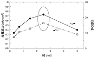
- FIG. 4 shows photocatalytic structures in which heterojunction nanorods 50 are formed with nanorods 30 as tungsten oxide (WO 3 ) and second material (light absorber) 40 as bismuth vanadium oxide (BiVO 4 ) at various heights H. It is a figure which shows the example which formed and measured the photocurrent value. In this figure, the left axis represents the photocurrent value (mA / cm 2 ), and the right axis represents IPCE (%).
- the inventors of the present invention determined that it is preferable to set the height of the nanorod 30 in a range of 500 nm ⁇ H ⁇ 2500 nm where a photocurrent greater than 0.3 mA / cm 2 can be obtained. is doing.
- FIG. 6 is a diagram showing an example of actual measurement of photocurrent values of the photocatalyst structure formed with an average thickness ⁇ R of various second materials (light absorbers) 40.
- the left axis represents the photocurrent value (mA / cm 2 )
- the right axis represents IPCE (%).
- the inventors have obtained an average thickness ⁇ R of the second material (light absorber) 40 in a range of 25 nm ⁇ R ⁇ 40 nm in which a value greater than 4 mA / cm 2 can be obtained as a photocurrent. Is determined to be preferable.
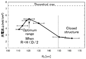
- FIG. 6 shows a heterojunction nanorod 50 in which the nanorod 30 is made of tungsten oxide (WO 3 ) and the second material (light absorber) 40 is made of bismuth vanadium oxide (BiVO 4 ), similar to those shown in FIGS. in the photocatalyst structure was formed, is a diagram showing an example of actual measurement of the photocurrent to form a radius R 2 of the heterojunction nanorods 50 at various values.
- the average radius R 2 of the heterojunction nanorod 50 needs to be set so as to satisfy R 2 ⁇ L / 2.
- the inventors of the present invention repeated the same experiment while changing the conditions for the average distance L between the heterojunction nanorods and the number N of nanorods per unit area ( ⁇ m 2 ), and the average distance L between the heterojunction nanorods was repeated. Is preferably in the range of 190 nm ⁇ L ⁇ 320 nm, and it has been concluded that the number N of nanorods per unit area ( ⁇ m 2 ) is preferably in the range of 10 ⁇ N ⁇ 30.
- the thickness of the light absorption layer containing BiVO 4 as a main component can be extremely reduced.
- the thickness of the light absorber covering the surface of the nanorods can be reduced. It can be made thinner than the diffusion length of electrons and holes therein. For this reason, the electron and the hole which were produced
- FIG. 7 is a diagram for conceptually explaining the principle when water splitting is performed using the photocatalyst structure according to the present invention.
- this photocatalyst structure is irradiated with light in an electrolyte 60 (buffer solution having a pH of about 7) such as Na 2 SO 4 and light is incident on the heterojunction nanorod 50, the photocatalyst structure is used as the second material (light absorber) 40.
- Active electrons and holes are formed in the surface region of bismuth vanadium oxide (BiVO 4 ), and these carriers cause a very strong redox reaction.
- the photogenerated electrons are injected into the conduction band of BiVO 4 and then move to the ITO film 20 through the nanorods 30 made of tungsten oxide (WO 3 ) which is a good conductor.
- the ITO film 20 moves from the back contact of the photoanode through the external circuit 70 to the Pt counter electrode (cathode) 80, and reduces water to generate hydrogen.
- holes are attracted to the Pt counter electrode 80 to oxidize water and generate oxygen. That is, irradiation of BiVO 4 with light generates electrons having a strong reducing power and holes having a strong oxidizing power, and these carriers react with water to generate hydrogen and oxygen. In this way, hydrogen is produced using light energy for water splitting.
- the efficiency of water decomposition by the photocatalyst is determined by the light absorption efficiency, the charge separation efficiency, and the catalyst conversion efficiency (injection efficiency). Of these properties, charge separation efficiency and catalytic conversion efficiency characterize the bulk and surface recombination processes.
- the thickness of the light absorber covering the surface of the nanorod can be made thinner than the diffusion length of carriers (electrons or holes) in the light absorber.
- the film thickness (the average thickness of the portion excluding the convex portion in the case of the aspect having the convex portion) can be only about 35 nm.
- FIG. 8 is a diagram for explaining one method for forming the above-described nanorods 30 made of tungsten oxide (WO 3 ) in an array on a substrate.
- tungsten oxide WO 3
- the glass substrate 10 having the ITO film 20 formed on the main surface is set on the sample holder 200, and the flux of WO 3 is supplied from the magnetron 300 which is the supply source of the first material. It is supplied to the surface of the ITO film 20.
- the sample holder 200 is variable not only in the in-plane rotation ( ⁇ ), but also the distance to the magnetron 300 and the viewing angle ( ⁇ ) with respect to the magnetron 300. By appropriately selecting these conditions, the average of the nanorods 30 is obtained. In addition to the radius R 1 , the average distance L between each other and the number N per unit area ( ⁇ m 2 ) can be controlled.
- the ITO film 20 provided on the glass substrate 10 may also be formed by the magnetron deposition method.
- the viewing angle ( ⁇ ) with respect to the magnetron 300 is also changed while the sample holder 200 is rotated in-plane ( ⁇ ), and the WO 3 is preferentially deposited in a specific direction due to the effect of shadowing. Avoid (FIG. 8B).
- the deposition of WO 3 is continued under such conditions, and the supply of the flux of WO 3 is stopped when the nanorod 30 reaches a desired height (for example, 2.5 ⁇ m), as shown in FIG.
- a desired height for example, 2.5 ⁇ m
- annealing is performed for about 4 to 5 hours at a temperature of about 560 ° C. in the atmosphere, for example, for the purpose of crystallization.
- the surface of the nanorod 30 of WO 3 obtained in this way is covered with a second material (light absorber) 40 having a photocatalytic action whose main component is bismuth vanadium oxide (BiVO 4 ).
- FIG. 9 is a view for explaining one method for coating the surface of the nanorod 30 of WO 3 with the second material (light absorber) 40.
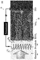
- the arrayed nanorods 30 formed by the above-described procedure are set in the electrodeposition apparatus 400.
- this electrodeposition apparatus 400 for example, 2M sodium acetate is prepared by dissolving 10 mM Bi (NO 3 ) 3 in 35 mM VOSO 4 to which pH is adjusted to 0.5 by adding HNO 3. An electrolyte whose pH is adjusted to 4.7 with a solution and a small amount of HNO 3 is filled. Electrodeposition is performed, for example, at a liquid temperature of 55 ° C. and a constant applied voltage of 0.21V.
- Nanorods 50 are formed.
- the coating with the second material (light absorber) 40 may be performed by a method other than the electrodeposition method, for example, the above-described magnetron deposition method.
- the second material (light absorber) 40 (BiVO 4 ) immediately after coating is in an amorphous state, annealing is performed for about 2 hours at a temperature of about 500 ° C., for example, in the atmosphere for crystallization. Apply.
- Cobalt phosphate (CoPi) having a photocatalytic action may be further deposited on the BiVO 4 in this state.
- the photo-assisted electrodeposition method PED method etc. can be used.
- the second material (light absorber) 40 includes not only BiVO 4 but also cobalt phosphate (CoPi) as a photocatalyst.
- the catalytic action is enhanced by using the co-photocatalyst, and as a result, the photocurrent and IPCE are remarkably increased.
- FIG. 11 shows a photocatalyst structure including a heterojunction nanorod 50 in which BiVO 4 and CoPi, which are second materials (light absorbers) 40 as a photocatalyst, are coated on the surface of a nanorod 30 of WO 3 ; It is a figure for demonstrating the result of having evaluated the characteristic under the bias of 1V.
- FIG. 11 (a) is a diagram showing a result of evaluation of IPCE (%) at 25 ° C. and 50 ° C. with respect to the wavelength (horizontal axis) of irradiation light.
- FIG. 11B is a diagram showing IV characteristics. Evaluation at 25 ° C. is performed with an irradiance amount of 1 SUN (1000 W / m 2 ) at AM 1.5G, and evaluation at 50 ° C. is performed with an irradiance amount of 3 SUN ( 3000 W / m 2 ).
- FIG. 11 (c) and FIG. 11 (d) show the hydrogen (H 2 ) and oxygen (O 2 ) gas production rates (circles) and faradaic efficiency ( ⁇ ) evaluated at 25 ° C. and 50 ° C., respectively.
- the broken line indicates the theoretical gas production rate.
- the time change of the photocurrent was shown in the lower part of these figures.
- substantially the same IPCE characteristics are obtained at 25 ° C. and 50 ° C., rising at a wavelength of 516 nm (2.4 eV), and the IPCE on the short wavelength side is , About 90% at 25 ° C. and about 92% at 50 ° C.
- the theoretical value of the photocurrent at 25 ° C. under a bias of 1V when AM1.5G is used is 6.73 mAcm ⁇ 2.
- the measured value is 6.72 mAcm ⁇ 2, which is an extremely high value.
- FIG. 12 is a diagram for explaining the results of evaluating the characteristics of a tandem type photovoltaic cell (PEC-PV cell) that was prototyped using the above-described photocatalytic structure according to the present invention as an anode (PEC cell).
- PEC-PV cell tandem type photovoltaic cell
- FIG. 12 (a) is a conceptual diagram showing the structure of the PEC-PV cell.
- FIG. 12B is a diagram showing the IV characteristics of the PEC-PV cell. Both the IV characteristics of the PEC cell and the IV characteristics of the PV cell are shown.
- the evaluation at 25 ° C. was performed with an irradiance amount of 1 SUN (1000 W / m 2 ) in AM1.5G, and the evaluation at 50 ° C. was performed with an irradiance amount of 3 SUN (3000 W / m 2 ).
- FIG. 12 (c) shows AM1.5G pseudo-sunlight spectrum and anode reflection spectrum. Furthermore, the solar energy utilization efficiency calculated based on the IPCE of the PEC-PV cell is shown as photon flux (photon flux). ) As an indicator.
- FIG. 12 (d) is a photocurrent profile of the PEC-PV cell. Evaluation at 25 ° C. is performed with an irradiance amount of 1 SUN (1000 W / m 2 ) at AM1.5G, and evaluation at 50 ° C. is an irradiance amount. Performed at 3 SUN (3000 W / m 2 ).
- the intersection of the IV curves of the PEC cell and the PV cell is 6.6 mA at 1.01 V at 25 ° C., and 18.6 at 1.02 V at 50 ° C. 3 mA.
- the anode is inclined at 45 ° with respect to the incident light, but the IV characteristic of the cell hardly depends on the light incident angle. It is understood that the catalytic action of the photocatalytic structure according to the present invention is governed by heterojunction nanorods arranged in an array.
- the IV characteristics are expected to decrease as the main surface of the support base of the photocatalyst is tilted from the light incident direction.
- the photocatalyst is formed as a heterojunction nanorod as in the invention and is arranged in an array, the effective amount of the photocatalyst that can contribute to the catalytic action even if the main surface of the support substrate is inclined from the light incident direction It is understood that it does not change much.
- the above description is based on an example in which the first material is WO 3 and the second material is BiVO 4.
- these oxides are merely examples, and The materials that can be employed in the invention are not limited to the combination of WO 3 and BiVO 4 .
- the combination of these materials is such that the main component of the nanorod is conductive, the main component of the light absorber has a photocatalytic action, and the band gap E g A of the nanorod is the band gap of the light absorber. It is wider than E g B (E g A > E g B ), and the energy E c A of the valence band of the nanorod is lower than the energy E c B of the light absorber (E c A ⁇ E c There can be various under the condition of B ).
- examples of the first material include MoO 3 and ZnO in addition to WO 3 .
- these materials are not limited to oxides and may be nitrides such as GaN, but are preferably materials that are stable in water.
- the surface of the light absorber film has a plurality of nanoparticle-like convex portions, and the plurality of convex portions define the average radius R 2 of the heterojunction nanorod. That is, in the embodiment illustrated in FIG. 1A, the second material (light absorber) 40 that covers the surface of the nanorod 30 has a thick portion (nanoparticle-like convex portion) and a thin portion (excluding the convex portion). In calculating the average radius R 2 of the heterojunction nanorod 50 described above, the average value of the thick portion is employed.
- the photocatalytic action is mainly brought about by the thick part of the second material (light absorber) 40, and the thick part (nanoparticle-like convex part) of the second material (light absorber).
- the diffusion of the carrier generated in the part) into the nanorod mainly occurs in the thin part (the part excluding the convex part) of the second material (light absorber).
- the light absorber film having a plurality of nanoparticle-like convex portions covers the nanorod surface with an average surface coverage C of 80% or more, in addition to the effect due to the high surface coverage, Combined with the effect that carriers generated under a high photocatalytic action can be efficiently diffused into nanorods, an extremely high quantum efficiency is realized.
- Table 1 summarizes various characteristics (examples) of such an embodiment and various characteristics (comparative example) of an embodiment (conventional structure) having a low surface coverage of nanorods (surface coverage of less than 20%).
- the main component of the nanorod is WO 3 and the main component of the light absorber is BiVO 4 .
- surface is what is called an external quantum efficiency
- a photocurrent is a value in voltage 1.2V RHE .
- the theoretical limit value of the photocurrent is 7.5 mA / cm 2 , it reaches 90% of the theoretical limit value in the example, and 47% of the theoretical limit value in the comparative example, which is about twice as much. It can be seen that a photocurrent of is obtained.
- the present invention provides a photocatalyst structure excellent in water decomposition efficiency and a photovoltaic cell comprising the same as an anode.
Landscapes
- Chemical & Material Sciences (AREA)
- Engineering & Computer Science (AREA)
- Organic Chemistry (AREA)
- Materials Engineering (AREA)
- Chemical Kinetics & Catalysis (AREA)
- Power Engineering (AREA)
- Health & Medical Sciences (AREA)
- General Health & Medical Sciences (AREA)
- Combustion & Propulsion (AREA)
- Inorganic Chemistry (AREA)
- Microelectronics & Electronic Packaging (AREA)
- Catalysts (AREA)
Abstract
本発明で採用するヘテロ接合構造(50)では、BiVO4などの光触媒は光吸収層(40)として作用し、その厚みを数十nm以下といった比較的薄いものとすることができる。この程度に薄い光触媒であれば、光吸収により発生した電子のほとんどを、電気伝導性に優れたナノロッド(30)で収集可能であるから、光生成キャリアの収集効率は格段に向上する。このように、本発明によれば、BiVO4をはじめとする光触媒を用いた従来の光電池の特性を遥かに凌ぐ優れた光電池を作製することが可能となる。
Description
本発明はナノロッド状の光触媒がアレイ配列された光触媒構造体に関し、より詳細には、水の分解効率に優れる光触媒構造体およびそれをアノードとして備える光電池に関する。
水素は、化学工業における基幹原料であり、また、クリーンエネルギー源でもある。従来の水素製造技術の殆どは、水蒸気改質(steam reforming)技術(非特許文献1)、石炭ガス化(coal gasification)技術(非特許文献2)、バイオマス熱分解(biomass pyrolysis)技術(非特許文献3)などの従来技術を基礎とするものである。このような技術では、化石燃料が用いられ、水素(H2)の製造に伴って大量の二酸化炭素(CO2)が発生することになる。しかし、化石燃料については資源の枯渇という問題があり、CO2排出についても地球温暖化などの環境問題がある。
これに対し、光触媒作用を利用して太陽光エネルギーを効率的に水分解させることにより水素を得る手法は、クリーンで再生可能な燃料を製造するための最も魅力的な方法のひとつと考えられている。この水素製造技術では、化石燃料を使うことがなくCO2排出もないため環境への負荷が少ない。そのため、持続可能でクリーンな、夢の水素製造技術として注目されている。
このような光触媒作用を利用した水分解システムの最も単純な構成は、光電池と水電解槽の組み合わせである。しかし、光電池と水電解槽の双方のエネルギー損失と設置に要する高いコストが、このようなシステムの実用化の妨げとなっているのが実情である。効率的な水素製造のためのもうひとつの選択として、水素の製造に太陽光エネルギーを直接利用する光電気化学電池(PEC:photoelectrochemical cell)がある。
典型的なPEC装置は、光吸収体としての半導体(フォトアノード)とPtなどの金属から成る対向電極を備え、これらが電解水溶液に浸漬される構成のものである。フォトアノードのバンドギャップよりも高いエネルギーの光子が照射されると、電子-正孔対が生成される。このうち、正孔は、フォトアノードと水の界面で水酸化反応に関与する。一方、電子は、フォトアノードのバックコンタクトから外部回路を通ってPt対向電極へと移動する。このようにして、太陽光エネルギーを水分解に利用した水素の製造に寄与することになる。
酸化チタン(TiO2)による水の光触媒分解現象(非特許文献4)が発見された後、この半導性酸化物は、光触媒作用の技術分野において最も研究対象とされた材料のひとつとなった。しかし、TiO2のバンドギャップは3.2eVであり、その光応答は太陽スペクトルの紫外線(UV)領域に制限されるため、水分解に利用できる太陽光のエネルギーは僅かに4%程度でしかない。つまり、太陽光エネルギーにより水を分解して水素に変換する効率(solar-to-hydrogen conversion efficiency)はその広いバンドギャップにより基本的な制限を受けてしまう。このような事情から、太陽スペクトルの可視光領域の利用を可能とする光触媒作用をもつ材料とこれを利用したシステムの開発のために、多くの努力がなされてきた。
太陽スペクトルの可視光領域の光を水分解に利用するためには、2~2.4eV程度の相対的にバンドギャップが小さな光触媒材料が求められ、そのような材料としては、BiVO4、α-Fe2O3、TaONなどを例示することができる。
例えば、ビスマスバナジウム酸塩(BiVO4)は、バンドギャップが約2.4eV程度(単斜晶型の場合)と比較的狭く、光腐食(photocorrosion)に対する安定性に優れ、しかも安価であるため、光触媒による水素製造のための最も有望視されている物質のひとつである(非特許文献5、6)。BiVO4の理論的なSTH(Solar-to-Hydrogen efficiency)、つまり太陽光エネルギーにより水を分解して水素に変換する効率は、日本付近の緯度の地上における平均的なスペクトルとして用いられるエアマス(AM1.5)の疑似太陽光照射条件(100mW/cm2)の下で、概ね7.5mA/cm2の最大光電流で、略9.2%にもなる。
BiVO4はこのように光吸収に優れている一方、光吸収により生じた電子と正孔の再結合率が高く、結晶中でのキャリアの拡散長は70nm程度と短くその電気伝導性は低い。そのため、光照射で生じた電子と正孔の再結合による水分解の動力学を妨げるという問題がある。BiVO4にMoやWをドーピングしてその電気伝導性を高める幾つかの試みもなされたが(非特許文献7、8)、その結果は何れも十分とは言えず、BiVO4の低い電気伝導性の問題は依然残されたままである。
α-Fe2O3も有望な材料であり、バンドギャップが2eV程度と小さく、太陽光スペクトルの約40%の範囲の光を吸収でき、理論的なエネルギー効率は15%程度と高い。しかし、結晶中での電子伝導度が低いことや電子と正孔の再結合率が高いなどの理由から、可視光領域の光の水分解への利用効率は大きく制限されてしまうという問題がある。
Rostrup-Nielsen, J.R.; Sehested, J.; Norskov, J.K.; Hydrogen and Syngas by Steam Reforming, Academic Press, 2002
David, A., Bell.; Brian, F., Towler.; Maohong Fan.; Coal Gasification and its Applications, Elsevier, 2010
Nowotny, J., Sorrell, C., Sheppard, L., Bak, T.; Solar-hydrogen: Environmentally safe fuel for the future. Int. J. Hydrogen Energy 30, 521-544 (2005)
Anpo, P., Kamat, P.,V.; Environmentally Benign Photocatalysts, Nanostructure Science and Technology, Springer Science+Busines Media, LLC 2010
Kudo, A., Ueda, K., Mikami, I.; Photocatalytic O2 evoluion under visible light irradiation on BiVO4 in aqueous AgNO3 solution, Catalysis Letters 53, 229-230 (1998)
Kudo, A., Omori, K. & Kato, H. Aqueous process for preparation of crystal form-controlled and highly crystalline BiVO4 powder from layered vanadates at room temperature and its photocatalytic. J. Am. Chem. Soc. 121, 11459-11467 (1999)
Pilli, S. K. et al. Cobalt-phosphate (Co-Pi) catalyst modified Mo-doped BiVO4 photoelectrodes for solar water oxidation. Energy Environ. Sci. 4, 5028-5034 (2011)
Ye, H., Park, H. & Bard, A. Screening of electrocatalysts for photoelectrochemical water oxidation on W-doped BiVO4 photocatalysts by scanning electrochemical microscopy. J. Phys. Chem. C 115, 12464-12470
このような事情を踏まえ、本発明者らは、水の分解効率を飛躍的に向上させる新規な光触媒構造体についての検討を進めてきた。本発明の目的は、可視光領域でも十分に高い光活性を有する光触媒と電気伝導性に優れる材料との組合せにより、水の分解効率に優れる光触媒構造体およびそれをアノードとして備える光電池を提供することにある。
上記課題を解決するために、本発明に係る光触媒構造体は、表面が導電性を有する基体上に、導電性を有する円柱状のナノロッドであって平均半径がR1のナノロッドが単位面積(μm2)当たりN本の密度で実質的に均一にアレイ状に設けられており、前記ナノロッドの表面は、光触媒作用を有する光吸収体膜により、平均表面被覆率Cで80%以上が被覆されて平均半径がR2のヘテロ接合ナノロッドを構成しており、前記ナノロッドのバンドギャップEg
Aは前記光吸収体のバンドギャップEg
Bより広く(Eg
A>Eg
B)、且つ、前記ナノロッドの価電子バンドのエネルギーEc
Aは前記光吸収体の価電子バンドのエネルギーEc
Bよりも低く(Ec
A<Ec
B)、前記ヘテロ接合ナノロッドの相互の平均間隔をLとしたときに前記平均半径R2がR2<L/2を満足している。
好ましくは、前記光吸収体膜の表面はナノ粒子状の凸部を複数有しており、該複数の凸部が前記ヘテロ接合ナノロッドの平均半径R2を規定する。
また、好ましくは、前記ナノロッドの表面を被覆する前記光吸収体膜の凸部を除く部分の平均厚みは、該光吸収体中における電子および正孔の拡散長よりも薄い。
また、好ましくは、前記光吸収体膜は、バンドギャップが3eV以下の直接遷移型の半導体材料である。
例えば、前記ナノロッドの主成分は、WO3、MoO3、ZnOの何れかである。
また、例えば、前記光吸収体の主成分は、BiVO4、BiFeO3、BiNbO4、BiTaO4、SbVO4、SbNbO4、SbTaO4、CrVO4、CrNbO4、CrTaO4、FeVO4、FeNbO4、FeTaO4、InVO4、InNbO4、InTaO4、LaVO4、LaNbO4、LaTaO4、CeVO4、CeNbO4、CeTaO4、α-Fe2O3、TaONの何れかである。
好ましくは、前記ナノロッドの主成分は酸化タングステン(WO3)であり、前記光吸収体の主成分は酸化ビスマスバナジウム(BiVO4)である。
また、好ましくは、前記光吸収体はリン酸コバルトを含む。
好ましい態様では、前記ヘテロ接合ナノロッドの平均半径R2と前記ナノロッドの平均半径R1の差ΔRが25nm<ΔR<40nmの範囲にある。
好ましくは、前記ナノロッドの平均半径R1は40nm<R1<100nmの範囲にある。
また、好ましくは、前記ナノロッドの高さHは500nm<H<2500nmの範囲にある。
さらに、好ましくは、前記ヘテロ接合ナノロッドの相互の平均間隔Lは190nm<L<320nmの範囲にある。
また、好ましくは、前記ナノロッドの単位面積(μm2)当たりの本数Nは10<N<30の範囲にある。
例えば、前記基体の表面は酸化インジウムスズ(ITO)であり、また、前記光吸収体膜は電着膜である。
本発明に係る光電池には、上述の光触媒構造体がアノードとして用いられている。
本発明で採用するヘテロ接合構造では、光触媒作用を有するBiVO4などの光吸収体の膜は光吸収層として作用し、その厚みを数十nm以下といった比較的薄いものとすることができる。この程度に薄い光吸収体であれば、光吸収により発生した電子のほとんどを、電気伝導性に優れたWO3などの材料から成るナノロッドで収集可能であるから、光生成キャリアの収集効率は格段に向上する。
また、光吸収体膜の表面にナノ粒子状の凸部を複数設けることとすると、該複数の凸部の存在により光吸収体の表面積が増大するため、光吸収により発生するキャリアの数も増加する。
このように、本発明によれば、BiVO4をはじめとする光触媒を用いた従来の光電池の特性を遥かに凌ぐ優れた光電池を作製することが可能となる。
以下に、図面を参照して、本発明の実施の形態について説明する。
なお、以降では、導電性を有する円柱状のナノロッドがWO3からなり、その表面を被覆する光触媒作用を有する光吸収体がBiVO4であるものとして本発明を説明するが、これらの材料はWO3とBiVO4に限定されるものではない。また、以降の説明では、主として、光吸収膜を電着法で蒸着する態様を説明するが、その際の蒸着法に特別な制限はない。
これらの材料の組合せは、ナノロッドの主成分が導電性を有するものであり、光吸収体の主成分が光触媒作用を有するものであって、ナノロッドのバンドギャップEg
Aは光吸収体のバンドギャップEg
Bより広く(Eg
A>Eg
B)、且つ、ナノロッドの価電子バンドのエネルギーEc
Aは光吸収体の価電子バンドのエネルギーEc
Bよりも低い(Ec
A<Ec
B)という条件のもとで、種々のものがあり得る。
ナノロッドの主成分としては、WO3の他に、MoO3やZnOを例示することができる。また、光吸収体の主成分としては、BiVO4の他に、BiFeO3、BiNbO4、BiTaO4、SbVO4、SbNbO4、SbTaO4、CrVO4、CrNbO4、CrTaO4、FeVO4、FeNbO4、FeTaO4、InVO4、InNbO4、InTaO4、LaVO4、LaNbO4、LaTaO4、CeVO4、CeNbO4、CeTaO4、α-Fe2O3、TaONなどを例示することができる。もちろん、これらの材料は酸化物に限定されるものではなく、GaNをはじめとする窒化物等であってもよい。
本発明では、光触媒による水素製造のために有望視されながらも、その低い電気伝導性のために本来の触媒特性を充分に生かすことが困難であった光触媒作用を有する材料の弱点を補うための新規な構造を提案する。具体的には、光触媒としての材料と導電性に優れた材料とのヘテロ接合構造を備えた光触媒構造体を提案する。
図1は、本発明に係る光触媒構造体の構成例を概念的に説明するための図で、図1(A)は上面図、図1(B)は断面図、そして、図1(C)は光吸収により発生した電子がナノロッドにより収集される様子を説明するための概念図である。
この光構造体は、導電性に優れた第1の材料を主成分とするナノロッドの表面を、光触媒作用を有する第2の材料が被覆している。第2の材料が光を吸収して発生したキャリア(電子)は、導電性に優れたナノロッドにより効率的に収集されることとなり、導電性が劣るという第2の材料の弱点を補うことができる。なお、この図に示した例では、ナノロッドは導電性に優れるWO3からなり、第2の材料は、光触媒作用に優れる酸化物として広く知られているBiVO4を主成分とするものである。
なお、上述のとおり、ナノロッドのバンドギャップEg
Aは光吸収体のバンドギャップEg
Bより広く(Eg
A>Eg
B)、且つ、ナノロッドの価電子バンドのエネルギーEc
Aは光吸収体の価電子バンドのエネルギーEc
Bよりも低い(Ec
A<Ec
B)という条件のもとで、上記第1および第2の材料の選択がなされる。
このような光構造体で採用されるヘテロ接合構造では、光触媒作用を有する光吸収体の膜(光吸収膜)は、例えば電着法により形成された膜(電着膜)であるため、その厚みを数十nm以下といった比較的薄いものとしつつ、ナノロッドの表面を高い被覆率で被覆することができる。つまり、ナノロッドの表面を被覆する光吸収体の厚みを、該光吸収体中におけるキャリア(電子もしくは正孔)の拡散長よりも薄くすることができる。
ナノロッドの表面を被覆する光吸収体の厚みが光吸収体中でのキャリアの拡散長よりも厚い場合には、発生したキャリアはナノロッド表面に拡散する途中で再結合により消滅してしまうが、本願発明では、ナノロッドの表面を被覆する光吸収体の厚みを、該光吸収体中におけるキャリア(電子もしくは正孔)の拡散長よりも薄くすることができる。そして、この程度に薄い光吸収体であれば、光吸収により発生したキャリアのほとんどを、導電性に優れたナノロッドで収集可能となり、光生成キャリアの収集効率は格段に向上する。
しかも、本願発明の光吸収体膜は、例えば電着法により形成された膜であるため、ナノロッドの表面を高い被覆率で被覆することができ、その分だけ光吸収量が増え、その結果、光生成キャリア量が顕著に向上する。
さらに、光吸収体膜を、例えば電着法により形成された膜とすると、当該電着膜の表面にナノ粒子状の凸部を複数形成することができ、このナノ粒子状の凸部の存在により光吸収体の表面積が増大するため、光吸収により発生するキャリアの数も増加する。
なお、このようなナノ粒子状の凸部を複数形成する場合には、ナノロッドの表面を被覆する光吸収体膜の凸部を除く部分の平均厚みが、該光吸収体中における電子および正孔の拡散長よりも薄くなるように成膜することになる。
図1に例示した光触媒構造体100では、基体としてのガラス基板10の表面に、導電性をもたせるための酸化インジウムスズの膜(ITO膜)20が形成されており、このITO膜20の上に、高さ(長さ)がHの、導電性を有する複数の円柱状のナノロッド30が、単位面積(μm2)当たりN本の密度で実質的に均一にアレイ状に設けられている。この図に示した例では、ナノロッド30を導電性に優れたものとするために、その主成分は、導電性に優れた酸化タングステン(WO3)とされている。なお、基板10はガラスに限定されるものではなく、その主面に形成される導電膜もITOに限定されるものではない。
このナノロッド30の表面を、主成分がBiVO4である光触媒作用を有する第2の材料から成る光吸収体40が被覆し、第1の酸化物との間でヘテロ接合を形成している。従って、この光触媒構造体100では、ITO膜20の上に、第1の材料と第2の材料のヘテロ接合が形成されたナノロッド50(ヘテロ接合ナノロッド)が、単位面積(μm2)当たりN本の密度で実質的に均一にアレイ状に設けられている。
ナノロッド30の平均半径をR1とし、ヘテロ接合ナノロッド50の平均半径をR2とすると、両者の差ΔRが、ナノロッド30の表面を被覆する第2の材料(光吸収体)40の平均厚みとなる。なお、上述のとおり、光吸収体40は、例えば電着法により形成された膜であり、ナノロッド30の表面を高い被覆率で被覆している。また、この図に示した態様では、光吸収体40である電着膜の表面はナノ粒子状の凸部を複数有しており、該複数の凸部がヘテロ接合ナノロッド50の平均半径R2を規定している。
ここで、太陽スペクトルの可視光領域の利用効率を高めるため、光吸収体40は、バンドギャップが3eV以下の直接遷移型の半導体材料であることが好ましい。このような材料を選択することで、太陽スペクトルの可視光領域の光の吸収効率が高まり、その結果、光エネルギーの利用効率が高まる。
また、ヘテロ接合ナノロッド50相互は、外部からの光がナノロッド30のガラス基板10側を被覆する第2の材料(光吸収体)40にも十分に到達できるように、離間されている。仮にこのようなヘテロ接合ナノロッド50相互の離間が妨げられると、光はヘテロ接合ナノロッド50の上部に形成された第2の材料(光吸収体)40によってのみ吸収されることとなり、それよりも下部の第2の材料(光吸収体)40は光吸収に寄与できず、光触媒作用を奏することができなくなる。
よって、本発明に係る光触媒構造体100では、ヘテロ接合ナノロッド50の相互の平均間隔をLとしたときに、ヘテロ接合ナノロッド50の平均半径をR2がR2<L/2を満足するように、アレイ状のナノロッド30の形成ならびに第2の材料(光吸収体)40の被覆がなされている。なお、この第2の材料(光吸収体)40のナノロッド30の平均表面被覆率Cは、80%以上であることが好ましい。
つまり、本発明に係る光触媒構造体の好ましい態様では、表面が導電性を有する基体上に、導電性を有する円柱状のナノロッドであって平均半径がR1のナノロッドが単位面積(μm2)当たりN本の密度で実質的に均一にアレイ状に設けられており、前記ナノロッドの表面は、光触媒作用を有する光吸収体膜により、平均表面被覆率Cで80%以上が被覆されて平均半径がR2のヘテロ接合ナノロッドを構成しており、前記ナノロッドのバンドギャップEg
Aは前記光吸収体のバンドギャップEg
Bより広く(Eg
A>Eg
B)、且つ、前記ナノロッドの価電子バンドのエネルギーEc
Aは前記光吸収体の価電子バンドのエネルギーEc
Bよりも低く(Ec
A<Ec
B)、前記ヘテロ接合ナノロッドの相互の平均間隔をLとしたときに前記平均半径R2がR2<L/2を満足している。
なお、図1(A)に図示しているように、ナノロッド30の表面を被覆する第2の材料(光吸収体)40は、厚い部分(ナノ粒子状の凸部)と薄い部分(凸部を除く部分)があるが、上述のヘテロ接合ナノロッド50の平均半径R2を算出するに際しては、厚い部分の平均的な値を採用している。尤も、薄い部分がナノロッド30の表面を被覆していないわけではないから、当該薄く被覆した第2の材料(光吸収体)40も光触媒作用を奏することは言うまでもないが、光触媒作用は主として、第2の材料(光吸収体)40の厚い部分によりもたらされる。
上述のとおり、図1に例示した構成のヘテロ接合構造では、BiVO4は光吸収層として作用し、その厚みを数十nm以下といった比較的薄いものとすることができる。この程度に薄いBiVO4であれば、光吸収により発生した電子のほとんどを、電気伝導性に優れたWO3を主成分とするナノロッドで収集可能であるから、光生成キャリアの収集効率は格段に向上する。このメカニズムは、上記2つの材料に限定されるものではなく、他の材料の組合せであっても同様である。
しかも、本発明に係る光触媒構造体100では、ヘテロ接合ナノロッド50が、単位面積(μm2)当たりN本の密度で実質的に均一にアレイ状に設けられており、ヘテロ接合ナノロッドの相互の平均間隔をLとしたときに、ヘテロ接合ナノロッド50の平均半径R2がR2<L/2を満足し、ヘテロ接合ナノロッド50相互が離間しているため、外部からの光がナノロッド30のガラス基板10側を被覆する第2の材料(光吸収体)40にも十分に到達できる。
そして、ヘテロ接合ナノロッド50の上部から入射した光は、当該部分に形成された第2の材料(光吸収体)40によって吸収されるだけではなく、ナノロッド30の表面と当該表面を薄く被覆する第2の材料(光吸収体)40との界面で反射を繰り返し、実質的な「光学的距離」が長くなるから、なお一層、第2の材料(光吸収体)40による光吸収率を高めること、すなわち、電子-正孔対の生成効率を高めることが可能となる。
このような光触媒構造体100を光電池のアノードとして用いた場合に光電流を最大化するためには、上記第2の材料(光吸収体)40の平均の厚み(ΔR)の最適化が必要となる。本発明者らの検討によれば、上記ΔRの最適値は、概ね、25nm<ΔR<40nmの範囲にある。
厚みが25nm以下だと、単位面積当たりの第2の材料(光吸収体)40による光吸収効率としてあまり高い値が得られない。一方、厚みが40nm以上だと、その相対的に低い電気伝導性のために、光吸収により発生した電子をナノロッドで収集する効率が低下してしまう。
上述した効果乃至傾向は、WO3とBiVO4の組合せに限らず、導電性に優れる第1の材料と光触媒作用に優れる第2の材料との組み合わせにおいても確認される効果乃至傾向であることは上述のとおりである。
例えば、第1の材料を、WO3、MoO3、ZnOの群から選択し、第2の材料を、BiVO4の他に、BiFeO3、BiNbO4、BiTaO4、SbVO4、SbNbO4、SbTaO4、CrVO4、CrNbO4、CrTaO4、FeVO4、FeNbO4、FeTaO4、InVO4、InNbO4、InTaO4、LaVO4、LaNbO4、LaTaO4、CeVO4、CeNbO4、CeTaO4、α-Fe2O3、TaONの群から選択し、これらの酸化物同士の組合せとしてもよい。
図2は、本発明に係る光触媒構造体のエネルギーバンド図の一例である。ガラス基板10上に導電性を有するITO膜20が形成され、その上に主成分が酸化タングステン(WO3)である円柱状のナノロッド30が単位面積(μm2)当たりN本の密度で実質的に均一にアレイ状に設けられ、これらナノロッド30の表面を、主成分が酸化ビスマスバナジウム(BiVO4)である光触媒作用を有する第2の材料(光吸収体)40が被覆してヘテロ接合ナノロッド50を形成している。
ヘテロ接合ナノロッド50にエネルギhνの光が入射すると、主成分が酸化ビスマスバナジウム(BiVO4)である光触媒作用を有する第2の材料(光吸収体)40中で電子-正孔対が形成される。光生成した電子は主成分が酸化タングステン(WO3)である良導体のナノロッド30を介してITO膜20へと移動し、さらに、フォトアノードのバックコンタクトから外部回路を通ってPt対向電極(不図示)へと移動する。一方、光生成した正孔は、フォトアノードと水の界面で水酸化反応に関与する。このようにして、光エネルギーを水分解に利用した水素の製造に寄与することになる。
このような構成の光触媒構造体において、光電流を最大化するパラメータ(例えば、ナノロッド30の高さH、第2の材料(光吸収体)40の平均の厚みΔR、ヘテロ接合ナノロッド50の平均半径R2)には適正な範囲がある。
図3は、これらのパラメータと光電変換効率(IPCE)との関係を概念的に示す図で、図3(A)はナノロッド30の高さH、図3(B)は第2の材料(光吸収体)40の平均の厚みΔR、図3(C)はヘテロ接合ナノロッド50の平均半径R2をパラメータとした場合の図である。
先ず、ナノロッド30の高さHをパラメータとした場合(図3(A))、H値が大きくなるにつれて光吸収量は徐々に高くなり、一定の値で飽和する。これは、当該一定値よりもH値が大きくなっても、基板に近い部分には光が照射され難くなることによると考えられる。一方、光電変換効率(IPCE:Incident Photon to Current conversion Efficiency)は概ねこの一定値を境に徐々に減少する傾向を示す。これは、ナノロッド30(ヘテロ接合ナノロッド50)のH値が大きくなると、それだけナノロッド30中を長く電子が伝導することとなるため、当該伝導の際に電気抵抗による損失が大きくなることによると考えられる。
つまり、ナノロッド30のH値が大きいほど光吸収量が増えてIPCEが増大する一方、ナノロッド30のH値が大きくなるほど電気抵抗による電子伝導損失が大きくなってIPCEが低下してしまう。このため、光電池としての効率を高めるためには、光電流を最大化するナノロッド30の高さHは適正範囲に設定することが必要となる。本発明では、このナノロッド30の高さHは、好ましくは500nm<H<2500nmの範囲に設定する。
次に、第2の材料(光吸収体40の平均の厚みΔRをパラメータとした場合(図3(B))、ΔR値が大きくなるにつれて光吸収量は徐々に高くなり、一定の値で飽和する。つまり、当該一定値よりもΔR値が大きくなっても、光吸収量は増大しない。
一方、光電変換効率(IPCE)は概ねこの一定値を境に徐々に減少する傾向を示す。これは、第2の材料(光吸収体)40が厚くなると、主成分(例えば酸化ビスマスバナジウム(BiVO4))はもともと導電性が低いため、第2の材料(光吸収体)40中を伝導する際に電気抵抗による損失が大きくなることによると考えられる。
つまり、第2の材料(光吸収体)40の平均の厚みΔRが大きいほど光吸収量が増えてIPCEが増大する一方、ΔRが大きくなるほど電気抵抗による電子伝導損失が大きくなってIPCEが低下してしまう。このため、光電池としての効率を高めるためには、光電流を最大化する第2の材料(光吸収体)40の平均の厚みΔRは適正範囲に設定することが必要となる。
本発明では、この第2の材料(光吸収体)40の平均の厚みΔR(すなわち、ヘテロ接合ナノロッド50の平均半径R2とナノロッド30の平均半径R1の差ΔR)は、好ましくは25nm<ΔR<40nmの範囲に設定する。
さらに、ヘテロ接合ナノロッド50の平均半径R2をパラメータとした場合(図3(C))、ヘテロ接合ナノロッド50の相互の平均間隔をLとしたときに平均半径R2がR2<L/2を満足しているか否かに、IPCEは大きく依存する。
平均半径R2がR2<L/2を満足している範囲では、R2値が大きくなるにつれて光吸収量は徐々に高くなり、最大値を示した後に減少し始める。これは、平均半径R2が大きくなるにつれて、隣接するヘテロ接合ナノロッド50との間隔が狭くなり、その結果、ヘテロ接合ナノロッド50の基板側への光入射量が減少することによるものと考えられる。
つまり、光電池としての効率を高めるためには、平均半径R2はR2<L/2を満足していることが必要であり、その範囲において平均半径R2を最適化することが必要となる。
本発明では、ヘテロ接合ナノロッド50の平均半径R2は、R2<L/2を満足するように設定し、好ましくは、ナノロッド30の平均半径R1を40nm<R1<100nmの範囲とし、ヘテロ接合ナノロッド50の平均半径R2とナノロッド30の平均半径R1の差ΔRを25nm<ΔR<40nmの範囲とし、さらに、ヘテロ接合ナノロッド50の相互の平均間隔Lを190nm<L<320nmの範囲に設定して、平均半径R2を設定する。
図4は、ナノロッド30を酸化タングステン(WO3)とし第2の材料(光吸収体)40を酸化ビスマスバナジウム(BiVO4)としてヘテロ接合ナノロッド50を形成した光触媒構造体を、種々の高さHで形成してその光電流値を実測した例を示す図である。この図において、左軸は光電流値(mA/cm2)を、右軸はIPCE(%)を示している。
図4に示した結果によれば、光電流およびIPCEは、酸化タングステン(WO3)からなるナノロッド30の高さHが大きくなるにつれて高くなるが、概ねH=2.5μm近傍で極大となり、これよりも大きなH値では減少してゆく。本発明者らは、この結果を基に、ナノロッド30の高さを、光電流として0.3mA/cm2よりも大きな値が得られる500nm<H<2500nmの範囲に設定することが好ましいと判断している。
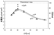
図5は、図4に示したものと同様に、ナノロッド30を酸化タングステン(WO3)とし第2の材料(光吸収体)40を酸化ビスマスバナジウム(BiVO4)としてヘテロ接合ナノロッド50を形成した光触媒構造体において、種々の第2の材料(光吸収体)40の平均の厚みΔRで形成してその光電流値を実測した例を示す図である。この図において、左軸は光電流値(mA/cm2)を、右軸はIPCE(%)を示している。
図5に示した結果によれば、光電流およびIPCEは、酸化ビスマスバナジウム(BiVO4)からなる第2の材料(光吸収体)40の平均の厚みΔRが大きくなるにつれて高くなるが、概ねΔR=30nm近傍で極大となり、これよりも大きなΔR値では減少してゆく。本発明者らは、この結果を基に、第2の材料(光吸収体)40の平均の厚みΔRを、光電流として4mA/cm2よりも大きな値が得られる25nm<ΔR<40nmの範囲に設定することが好ましいと判断している。
図6は、図4および図5に示したものと同様に、ナノロッド30を酸化タングステン(WO3)とし第2の材料(光吸収体)40を酸化ビスマスバナジウム(BiVO4)としてヘテロ接合ナノロッド50を形成した光触媒構造体において、ヘテロ接合ナノロッド50の半径R2を種々の値で形成してその光電流値を実測した例を示す図である。
この図に示した結果から明らかなように、光電池としての効率を高めるためには、ヘテロ接合ナノロッド50の平均半径R2は、R2<L/2を満足するように設定する必要がある。
本発明者らは、ヘテロ接合ナノロッドの相互の平均間隔Lおよびナノロッドの単位面積(μm2)当たりの本数Nについての条件を変更して同様の実験を繰り返し、ヘテロ接合ナノロッドの相互の平均間隔Lは190nm<L<320nmの範囲にあることが好ましく、ナノロッドの単位面積(μm2)当たりの本数Nは10<N<30の範囲にあることが好ましいと結論付けるに至った。
上述した構造の光触媒構造体を用いると、BiVO4を主成分とする光吸収層の厚みを極めて薄くすることができ、例えば、ナノロッドの表面を被覆する光吸収体の厚みを、該光吸収体中における電子および正孔の拡散長よりも薄くすることができる。このため、光照射により生成した電子と正孔が効率的に水分解に寄与し、これをアノードとして用いた場合の光電池の効率を高めることができる。
図7は、本発明に係る光触媒構造体を用いて水分解を行う際の原理を概念的に説明するための図である。この光触媒構造体は、例えばNa2SO4などの電解質60(pH7程度の緩衝溶液)中で光照射され、ヘテロ接合ナノロッド50に光が入射すると、第2の材料(光吸収体)40としての酸化ビスマスバナジウム(BiVO4)の表面領域で、活性な電子と正孔が形成され、これらのキャリアが極めて強い酸化還元反応を引き起こす。
光生成した電子は、BiVO4の伝導帯に注入された後、良導体である酸化タングステン(WO3)からなるナノロッド30を介してITO膜20へと移動する。このITO膜20はフォトアノードのバックコンタクトから外部回路70を通ってPt対向電極(カソード)80へと移動し、水を還元して水素を発生させる。
一方、正孔はPt対向電極80に引き寄せられて水を酸化して酸素を発生させる。つまり、BiVO4への光照射により、強い還元力をもつ電子と強い酸化力をもつ正孔が生成され、これらのキャリアが水と反応して水素と酸素を発生させる。このようにして、光エネルギーを水分解に利用した水素の製造が行われる。
光触媒による水分解の効率は、光吸収効率、電荷分離効率、および、触媒変換効率(注入効率)によって決まる。これらの特性のうち、電荷分離効率と触媒変換効率は、バルクおよび表面での再結合過程を特徴付けるものである。
また、水分解による光電流(Jp)は、電流密度として評価される光吸収効率(JA)と、アノードと電解質の界面に到達する光生成した正孔の割合(Psep)と、水分解のために電解質に注入される光生成した正孔の割合(Pinj)との積(Jp=JA×Psep×Pinj)で与えられる。
本願発明の場合、ナノロッドの表面を被覆する光吸収体の厚みを、該光吸収体中におけるキャリア(電子もしくは正孔)の拡散長よりも薄くすることができる。例えば、光吸収体がBiVO4であるとした場合の膜厚(凸部を有する態様の場合には凸部を除く部分の平均厚み)を僅か35nm程度とすることができる。
この厚みは、BiVO4中のキャリア(正孔)の拡散長(約80nm)よりも遥かに薄いから、Psep(アノードと電解質の界面に到達する光生成した正孔の割合)は略1となる。その結果、本願発明により極めて高い光電流(Jp)を得ることが可能となる。
以下に、本発明に係る光触媒構造体が備えるヘテロ接合ナノロッド50の形成法を、例示により説明する。
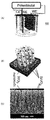
図8は、上述した酸化タングステン(WO3)からなるナノロッド30を基板上にアレイ状に形成するための一手法を説明するための図である。
図8(A)に図示したように、主面にITO膜20が形成されたガラス基板10を試料ホルダ200にセットし、第1の材料の供給源であるマグネトロン300から、WO3のフラックスが上記ITO膜20の表面に供給される。試料ホルダ200は、面内での回転(φ)はもとより、マグネトロン300との距離およびマグネトロン300に対する視射角(α)も可変であり、これらの条件を適宜選択することにより、ナノロッド30の平均半径R1はもとより、相互の平均間隔Lや単位面積(μm2)当たりの本数Nも制御することができる。なお、ガラス基板10上に設けるITO膜20もまた、上記マグネトロン堆積法で形成するようにしてもよい。
WO3の堆積中、試料ホルダ200を面内回転(φ)させながらマグネトロン300に対する視射角(α)も変化させ、シャドーイングの効果により特定方向に優先的にWO3が堆積されることを回避する(図8(B))。このような条件でWO3の堆積を継続し、ナノロッド30が所望の高さ(例えば2.5μm)となった時点でWO3のフラックス供給を停止すると、図8(C)に図示したような、単位面積(μm2)当たりN本の密度で実質的に均一にアレイ状に設けられた状態の円柱状のナノロッド30が得られる。
なお、この堆積直後のWO3のナノロッド30はアモルファス状態にあるため、結晶化の目的で、例えば大気中で、560℃程度の温度で4~5時間程度のアニールを施す。
続いて、このようにして得られたWO3のナノロッド30の表面を、主成分が酸化ビスマスバナジウム(BiVO4)である光触媒作用を有する第2の材料(光吸収体)40で被覆する。
図9は、WO3のナノロッド30の表面に第2の材料(光吸収体)40を被覆するための一手法を説明するための図である。図9(A)に示したように、上述の手順で形成されたアレイ状のナノロッド30を、電着装置400内にセットする。この電着装置400内には、例えば、HNO3を添加してpHが0.5とされた35mMのVOSO4中に10mMのBi(NO3)3を溶解させたものを、2Mの酢酸ソーダ溶液と微量のHNO3でpHを4.7に調整した電解質が充填されている。電着は、例えば55℃の液温で一定の印加電圧0.21Vで行う。
この電着により、図9(B)および図9(C)に示したように、WO3のナノロッド30の表面が第2の材料(光吸収体)40(BiVO4)により被覆され、ヘテロ接合ナノロッド50が形成される。
なお、第2の材料(光吸収体)40による被覆は電着法以外の手法で行ってもよく、例えば、上述したマグネトロン堆積法で行うようにしてもよい。
このような被覆直後の第2の材料(光吸収体)40(BiVO4)はアモルファス状態にあるため、結晶化の目的で、例えば大気中で、500℃程度の温度で2時間程度のアニールを施す。
この状態のBiVO4の上から、さらに、光触媒作用を有するリン酸コバルト(CoPi)を蒸着するようにしてもよい。その際の蒸着法に特別な制限はないが、例えば、光アシスト電着法(PED法)などによることができる。この場合、第2の材料(光吸収体)40は、BiVO4だけではなく、リン酸コバルト(CoPi)も光触媒として含むこととなる。
図10は、図5に、ΔR=30nmの条件において、第2の材料(光吸収体)40をBiVO4とリン酸コバルトの共光触媒とした場合の光電流およびIPCEのデータを付加した図である。
図10に示した結果によれば、共光触媒としたことにより触媒作用が強まり、その結果、光電流およびIPCEが顕著に高くなっている。
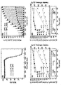
図11は、WO3のナノロッド30の表面に、光触媒としての第2の材料(光吸収体)40であるBiVO4とCoPiを被覆させたヘテロ接合ナノロッド50を備える光触媒構造体を作製し、その特性を1Vのバイアス下で評価した結果を説明するための図である。
図11(a)は照射光の波長(横軸)に対するIPCE(%)を25℃と50℃で評価した結果の図である。
図11(b)はI-V特性を示す図であり、25℃での評価はAM1.5Gにおける放射照度量1SUN(1000W/m2)で行い、50℃での評価は放射照度量3SUN(3000W/m2)で行った。
図11(c)および図11(d)はそれぞれ、25℃および50℃で評価した、水素(H2)および酸素(O2)のガス生成率(○マーク)、ファラデー効率(faradaic efficiency:□マーク)であり、破線は理論ガス生成率を示している。また、これらの図の下部には、光電流の時間変化を示した。
図11(a)の結果によれば、25℃と50℃において、概ね同様のIPCE特性(波長依存性)が得られており、波長516nm(2.4eV)で立ち上がり、短波長側のIPCEは、25℃において90%程度、50℃において92%程度である。
図11(b)に示したI-V特性をみると、先ず、AM1.5Gとした際の1Vのバイアス下における25℃での光電流の理論値が6.73mAcm-2であるのに対し、実測値は6.72mAcm-2であり、極めて高い値が得られている。
AM1.5Gとした際の1Vのバイアス下における50℃での光電流についても、理論値20.9mAcm-2に対し実測値は18.2mAcm-2であり、極めて高い値が得られている。
次に、水素(H2)のガス生成率についてみると、図11(c)に示した結果から、25℃において102μmolh-1cm-2(1SUNの光照射量の場合)、50℃において281μmolh-1cm-2(3SUNの光照射量の場合)と求まる。また、ファラデー効率については、光照射後の15分で既に80%に達し、概ね85%程度まで上昇する。
図12は、上述の本発明に係る光触媒構造体をアノード(PECセル)として試作したタンデム型の光電池(PEC-PVセル)の特性を評価した結果を説明するための図である。
図12(a)は当該PEC-PVセルの構造を示す概念図である。
図12(b)は当該PEC-PVセルのI-V特性を示す図であり、PECセルのI-V特性PVセルのI-V特性の双方が示されている。なお、25℃での評価はAM1.5Gにおける放射照度量1SUN(1000W/m2)で行い、50℃での評価は放射照度量3SUN(3000W/m2)で行った。
図12(c)にはAM1.5Gの疑似太陽光のスペクトルおよびアノードの反射スペクトルを示しており、さらに、当該PEC-PVセルのIPCEを基に算出した太陽エネルギー利用効率を光子束(photon flux)を指標として示している。
図12(d)は当該PEC-PVセルの光電流プロファイルであり、25℃での評価はAM1.5Gにおける放射照度量1SUN(1000W/m2)で行い、50℃での評価は放射照度量3SUN(3000W/m2)で行った。
図12(b)に示したI-V特性をみると、PECセルとPVセルのIV曲線の交点は、25℃では1.01Vにおいて6.6mAであり、50℃では1.02Vにおいて18.3mAである。
なお、図12(a)に示したように、アノードは入射光に対して45°傾いて設けられているが、セルのI-V特性は光入射角に殆ど依存することはなかった。これは、本発明に係る光触媒構造体の触媒作用は、アレイ状に配置されたヘテロ接合ナノロッドが司ることによるものと理解している。
つまり、光触媒が2次元的(平面的)に設けられている場合には、光触媒の支持基体の主面が光の入射方向から傾くほどI-V特性は低下することが予想されるが、本発明のように光触媒がヘテロ接合ナノロッドとして形成され、しかもそれがアレイ状に配置されている場合には、支持基体の主面が光の入射方向から傾いても触媒作用に寄与できる光触媒の実効量はさほど変化しないものと理解される。
次に、図12(d)に示した光電流プロファイルを見ると、25℃は6.56mA、50℃では18.17mAの光電流が得られている。このうち、6.56mAという数値は、太陽光水素(STH)変換の理論効率の8.1%に相当し、BiVO4:W,Mo/a-Si型の2接合タンデムセルについて従来報告されているSTH変換効率4.92%の1.6倍となる。また、18.17mAという数値は、STH変換の理論効率の7.5%に相当する。
このように、本発明によれば、BiVO4をはじめとする光触媒を用いた従来の光電池の特性を遥かに凌ぐ優れた光電池を作製することが可能となる。
なお、既に述べたとおり、上述の説明は、第1の材料をWO3とし、第2の材料がBiVO4である場合についての例示に基づくが、これらの酸化物はあくまでも一例に過ぎず、本発明で採用し得る材料は、WO3とBiVO4の組合せに限定されるものではない。
これらの材料の組合せは、ナノロッドの主成分が導電性を有するものであり、光吸収体の主成分が光触媒作用を有するものであって、ナノロッドのバンドギャップEg
Aは光吸収体のバンドギャップEg
Bより広く(Eg
A>Eg
B)、且つ、ナノロッドの価電子バンドのエネルギーEc
Aは光吸収体の価電子バンドのエネルギーEc
Bよりも低い(Ec
A<Ec
B)という条件のもとで、種々のものがあり得る。
例えば、第1の材料としては、WO3の他に、MoO3やZnOを例示することができる。
また、例えば、第2の材料としては、BiVO4の他に、BiFeO3、BiNbO4、BiTaO4、SbVO4、SbNbO4、SbTaO4、CrVO4、CrNbO4、CrTaO4、FeVO4、FeNbO4、FeTaO4、InVO4、InNbO4、InTaO4、LaVO4、LaNbO4、LaTaO4、CeVO4、CeNbO4、CeTaO4、α-Fe2O3、TaONなどを例示することができる。
もちろん、これらの材料は酸化物に限定されるものではなく、GaNをはじめとする窒化物等であってもよいが、水中で安定な材料であることが好ましい。
上述した第1の材料と第2の材料の組合せであれば、本発明が奏する効果を得ることができる。
本発明の好ましい態様では、光吸収体膜の表面はナノ粒子状の凸部を複数有しており、該複数の凸部がヘテロ接合ナノロッドの平均半径R2を規定する。つまり、図1(A)に図示した態様では、ナノロッド30の表面を被覆する第2の材料(光吸収体)40は、厚い部分(ナノ粒子状の凸部)と薄い部分(凸部を除く部分)を有しており、上述のヘテロ接合ナノロッド50の平均半径R2を算出するに際しては、厚い部分の平均的な値を採用する。
そして、既に説明したように、光触媒作用は主として、第2の材料(光吸収体)40の厚い部分によりもたらされ、当該第2の材料(光吸収体)の厚い部分(ナノ粒子状の凸部)で生じたキャリアのナノロッドへの拡散は主として、第2の材料(光吸収体)の薄い部分(凸部を除く部分)で起こる。
つまり、ナノ粒子状の凸部を複数有する光吸収体膜が80%以上の平均表面被覆率Cでナノロッド表面を被覆している態様では、その表面被覆率の高さに起因する効果に加え、高い光触媒作用の下で発生したキャリアを効率的にナノロッドへに拡散させ得るという効果が相俟って、極めて高い量子効率が実現される。
このような態様のものの諸特性(実施例)と、ナノロッドの表面被覆率が低い態様(表面被覆率20%未満)のもの(従来構造)の諸特性(比較例)を、表1に纏めた。何れのものも、ナノロッドの主成分はWO3であり、光吸収体の主成分はBiVO4である。なお、表中の量子効率(IPCE:Incident to photon conversion efficiency)はいわゆる外部量子効率であり、光電流は電圧1.2VRHEにおける値である。

光電流の理論限界値は7.5mA/cm2であるから、実施例のものでは理論限界値の90%に達しており、比較例のものでは理論限界値の47%であり、約2倍の光電流が得られていることが分かる。
本発明は、水の分解効率に優れる光触媒構造体およびそれをアノードとして備える光電池を提供する。
10 ガラス基板
20 ITO膜
30 ナノロッド
40 第2の材料(光吸収体)
50 ヘテロ接合ナノロッド
60 電解質
70 外部回路
80 カソード
100 光触媒構造体
200 試料ホルダ
300 マグネトロン
400 電着装置
20 ITO膜
30 ナノロッド
40 第2の材料(光吸収体)
50 ヘテロ接合ナノロッド
60 電解質
70 外部回路
80 カソード
100 光触媒構造体
200 試料ホルダ
300 マグネトロン
400 電着装置
Claims (16)
- 表面が導電性を有する基体上に、
導電性を有する円柱状のナノロッドであって平均半径がR1のナノロッドが単位面積(μm2)当たりN本の密度で実質的に均一にアレイ状に設けられており、
前記ナノロッドの表面は、光触媒作用を有する光吸収体膜により、平均表面被覆率Cで80%以上が被覆されて平均半径がR2のヘテロ接合ナノロッドを構成しており、
前記ナノロッドのバンドギャップEg Aは前記光吸収体のバンドギャップEg Bより広く(Eg A>Eg B)、且つ、前記ナノロッドの価電子バンドのエネルギーEc Aは前記光吸収体の価電子バンドのエネルギーEc Bよりも低く(Ec A<Ec B)、
前記ヘテロ接合ナノロッドの相互の平均間隔をLとしたときに前記平均半径R2がR2<L/2を満足している、光触媒構造体。 - 前記光吸収体膜の表面はナノ粒子状の凸部を複数有しており、該複数の凸部が前記ヘテロ接合ナノロッドの平均半径R2を規定する、請求項1に記載の光触媒構造体。
- 前記ナノロッドの表面を被覆する前記光吸収体膜の凸部を除く部分の平均厚みは、該光吸収体中における電子および正孔の拡散長よりも薄い、請求項2に記載の光触媒構造体。
- 前記光吸収体膜は、バンドギャップが3eV以下の直接遷移型の半導体材料である、請求項1~3の何れか1項に記載の光触媒構造体。
- 前記ナノロッドの主成分は、WO3、MoO3、ZnOの何れかである、請求項1~3の何れか1項に記載の光触媒構造体。
- 前記光吸収体の主成分は、BiVO4、BiFeO3、BiNbO4、BiTaO4、SbVO4、SbNbO4、SbTaO4、CrVO4、CrNbO4、CrTaO4、FeVO4、FeNbO4、FeTaO4、InVO4、InNbO4、InTaO4、LaVO4、LaNbO4、LaTaO4、CeVO4、CeNbO4、CeTaO4、α-Fe2O3、TaONの何れかである、請求項1~3の何れか1項に記載の光触媒構造体。
- 前記ナノロッドの主成分は酸化タングステン(WO3)であり、前記光吸収体の主成分は酸化ビスマスバナジウム(BiVO4)である、請求項6に記載の光触媒構造体。
- 前記光吸収体はリン酸コバルトを含む、請求項1~3の何れか1項に記載の光触媒構造体。
- 前記ヘテロ接合ナノロッドの平均半径R2と前記ナノロッドの平均半径R1の差ΔRが25nm<ΔR<40nmの範囲にある、請求項1~3の何れか1項に記載の光触媒構造体。
- 前記ナノロッドの平均半径R1は40nm<R1<100nmの範囲にある、請求項1~3の何れか1項に記載の光触媒構造体。
- 前記ナノロッドの高さHは500nm<H<2500nmの範囲にある、請求項1~3の何れか1項に記載の光触媒構造体。
- 前記ヘテロ接合ナノロッドの相互の平均間隔Lは190nm<L<320nmの範囲にある、請求項1~3の何れか1項に記載の光触媒構造体。
- 前記ナノロッドの単位面積(μm2)当たりの本数Nは10<N<30の範囲にある、請求項1~3の何れか1項に記載の光触媒構造体。
- 前記基体の表面は酸化インジウムスズ(ITO)である、請求項1~3の何れか1項に記載の光触媒構造体。
- 前記光吸収体膜は電着膜である、請求項1~3の何れか1項に記載の光触媒構造体。
- 請求項1~3の何れか1項に記載の光触媒構造体がアノードとして用いられている光電池。
Priority Applications (1)
| Application Number | Priority Date | Filing Date | Title |
|---|---|---|---|
| JP2017502000A JPWO2016136374A1 (ja) | 2015-02-26 | 2016-01-28 | 光触媒構造体および光電池 |
Applications Claiming Priority (2)
| Application Number | Priority Date | Filing Date | Title |
|---|---|---|---|
| JP2015-037227 | 2015-02-26 | ||
| JP2015037227 | 2015-02-26 |
Publications (1)
| Publication Number | Publication Date |
|---|---|
| WO2016136374A1 true WO2016136374A1 (ja) | 2016-09-01 |
Family
ID=56788407
Family Applications (1)
| Application Number | Title | Priority Date | Filing Date |
|---|---|---|---|
| PCT/JP2016/052531 Ceased WO2016136374A1 (ja) | 2015-02-26 | 2016-01-28 | 光触媒構造体および光電池 |
Country Status (2)
| Country | Link |
|---|---|
| JP (1) | JPWO2016136374A1 (ja) |
| WO (1) | WO2016136374A1 (ja) |
Cited By (14)
| Publication number | Priority date | Publication date | Assignee | Title |
|---|---|---|---|---|
| CN108704652A (zh) * | 2018-06-01 | 2018-10-26 | 苏州大学张家港工业技术研究院 | 氟氯钽酸铋及其制备方法和应用 |
| JPWO2017131226A1 (ja) * | 2016-01-29 | 2018-11-22 | 高砂香料工業株式会社 | N,n−ビス(2−ジアルキルホスフィノエチル)アミン−ボラン錯体及びその製造法、並びにn,n−ビス(2−ジアルキルホスフィノエチル)アミンを配位子とするルテニウム錯体の製造方法 |
| CN109772294A (zh) * | 2019-03-18 | 2019-05-21 | 济南大学 | 一种具有p型导电性的四方相BiVO4薄膜的制备方法及所得产品和应用 |
| CN110042407A (zh) * | 2019-03-15 | 2019-07-23 | 江苏大学 | 磷酸钴-聚多巴胺-钒酸铋三元复合光电极的制备方法及应用 |
| CN111359621A (zh) * | 2020-03-09 | 2020-07-03 | 南昌航空大学 | 一种光催化降解复合颗粒及其制备方法和应用 |
| CN111841606A (zh) * | 2020-07-23 | 2020-10-30 | 中国环境科学研究院 | 一种非均相FeVO4催化材料及其制备方法和应用 |
| CN112981449A (zh) * | 2019-12-14 | 2021-06-18 | 中国科学院大连化学物理研究所 | 一种有序化的pem水电解膜电极阳极催化层及其制备方法与应用 |
| CN113990675A (zh) * | 2021-09-30 | 2022-01-28 | 南京大学 | 一种用于高性能太阳能充电器件的CoPi/BiVO4法拉第光电极材料及其制备方法 |
| KR20220088125A (ko) * | 2020-12-18 | 2022-06-27 | 고려대학교 산학협력단 | 금속 메쉬를 도입한 저저항 투명전극의 제조방법 |
| CN115710716A (zh) * | 2022-11-30 | 2023-02-24 | 东北大学佛山研究生创新学院 | CoPi负载的枝状(GaN)1-x(ZnO)x-GaN纳米线阵列光阳极及制备方法 |
| US12247281B2 (en) | 2022-10-24 | 2025-03-11 | King Fahd University Of Petroleum And Minerals | Method for coating a substrate with a Co-PI modified BiVO4/WO3 heterostructure film |
| CN119838625A (zh) * | 2025-01-24 | 2025-04-18 | 上海应用技术大学 | 一种Bi4TaO8Cl@g-C3N4复合纳米材料及其制备方法和应用 |
| CN119869569A (zh) * | 2025-01-20 | 2025-04-25 | 昆明理工大学 | 一种Fe2O3-Bi4TaO8Br光芬顿催化剂的制备方法及应用 |
| JP7866731B1 (ja) * | 2025-11-06 | 2026-05-28 | 江▲蘇▼大学 | InNbO4光触媒及びその調製方法並びに用途 |
Families Citing this family (1)
| Publication number | Priority date | Publication date | Assignee | Title |
|---|---|---|---|---|
| CN118937423B (zh) * | 2024-10-14 | 2025-03-18 | 山东海化集团有限公司 | 一种WO3-FeVO4气敏材料的制备方法及其应用 |
Citations (1)
| Publication number | Priority date | Publication date | Assignee | Title |
|---|---|---|---|---|
| WO2014174824A1 (ja) * | 2013-04-26 | 2014-10-30 | パナソニック株式会社 | 光半導体電極、およびそれを具備する光電気化学セル用いて水を光分解する方法 |
-
2016
- 2016-01-28 WO PCT/JP2016/052531 patent/WO2016136374A1/ja not_active Ceased
- 2016-01-28 JP JP2017502000A patent/JPWO2016136374A1/ja active Pending
Patent Citations (1)
| Publication number | Priority date | Publication date | Assignee | Title |
|---|---|---|---|---|
| WO2014174824A1 (ja) * | 2013-04-26 | 2014-10-30 | パナソニック株式会社 | 光半導体電極、およびそれを具備する光電気化学セル用いて水を光分解する方法 |
Non-Patent Citations (4)
| Title |
|---|
| OSAMU WATANABE ET AL.: "ZnO-(GaN:ZnO) Core/ Shell-Gata Nanorod Hikari Yokyoku o Mochiita Hikari Shokubaiteki Suibunkai ni yoru Suiso Seisei Hanno", CSJ: THE CHEMICAL SOCIETY OF JAPAN KOEN YOKOSHU, vol. 94, no. 2, 12 March 2014 (2014-03-12), pages 518 * |
| YURIY PIHOSH ET AL.: "Nanostructured WO 3/BiV04 Photoanodes for Efficient Photoelectrochemical Water Splitting", SMALL, vol. 10, no. 18, 24 September 2014 (2014-09-24), pages 3692 - 3699 * |
| YURIY PIHOSH ET AL.: "WO 3-NRs/BiV04 core-shell nanostructure for enhanced photocatalytic H2 production", JSAP SPRING MEETING KOEN YOKOSHU ( CD-ROM, vol. 62, 26 February 2015 (2015-02-26), pages 11P-D9 - 7 * |
| ZHEN XU ET AL.: "Effect of CoOOH loading on the photoelectrocatalytic performance of WO 3 nanorod array film", APPLIED SURFACE SCIENCE, vol. 284, 1 November 2013 (2013-11-01), pages 285 - 290, XP028710369, DOI: doi:10.1016/j.apsusc.2013.07.095 * |
Cited By (20)
| Publication number | Priority date | Publication date | Assignee | Title |
|---|---|---|---|---|
| JPWO2017131226A1 (ja) * | 2016-01-29 | 2018-11-22 | 高砂香料工業株式会社 | N,n−ビス(2−ジアルキルホスフィノエチル)アミン−ボラン錯体及びその製造法、並びにn,n−ビス(2−ジアルキルホスフィノエチル)アミンを配位子とするルテニウム錯体の製造方法 |
| CN108704652A (zh) * | 2018-06-01 | 2018-10-26 | 苏州大学张家港工业技术研究院 | 氟氯钽酸铋及其制备方法和应用 |
| CN110042407A (zh) * | 2019-03-15 | 2019-07-23 | 江苏大学 | 磷酸钴-聚多巴胺-钒酸铋三元复合光电极的制备方法及应用 |
| CN109772294A (zh) * | 2019-03-18 | 2019-05-21 | 济南大学 | 一种具有p型导电性的四方相BiVO4薄膜的制备方法及所得产品和应用 |
| CN109772294B (zh) * | 2019-03-18 | 2021-12-07 | 济南大学 | 一种具有p型导电性的四方相BiVO4薄膜的制备方法及所得产品和应用 |
| CN112981449A (zh) * | 2019-12-14 | 2021-06-18 | 中国科学院大连化学物理研究所 | 一种有序化的pem水电解膜电极阳极催化层及其制备方法与应用 |
| CN112981449B (zh) * | 2019-12-14 | 2022-01-11 | 中国科学院大连化学物理研究所 | 一种有序化的pem水电解膜电极阳极催化层及其制备方法与应用 |
| CN111359621A (zh) * | 2020-03-09 | 2020-07-03 | 南昌航空大学 | 一种光催化降解复合颗粒及其制备方法和应用 |
| CN111841606A (zh) * | 2020-07-23 | 2020-10-30 | 中国环境科学研究院 | 一种非均相FeVO4催化材料及其制备方法和应用 |
| CN111841606B (zh) * | 2020-07-23 | 2021-03-12 | 中国环境科学研究院 | 一种非均相FeVO4催化材料及其制备方法和应用 |
| KR102519888B1 (ko) * | 2020-12-18 | 2023-04-10 | 고려대학교 산학협력단 | 금속 메쉬를 도입한 저저항 투명전극의 제조방법 |
| KR20220088125A (ko) * | 2020-12-18 | 2022-06-27 | 고려대학교 산학협력단 | 금속 메쉬를 도입한 저저항 투명전극의 제조방법 |
| CN113990675A (zh) * | 2021-09-30 | 2022-01-28 | 南京大学 | 一种用于高性能太阳能充电器件的CoPi/BiVO4法拉第光电极材料及其制备方法 |
| CN113990675B (zh) * | 2021-09-30 | 2023-01-06 | 南京大学 | 一种用于高性能太阳能充电器件的CoPi/BiVO4法拉第光电极材料及其制备方法 |
| US12247281B2 (en) | 2022-10-24 | 2025-03-11 | King Fahd University Of Petroleum And Minerals | Method for coating a substrate with a Co-PI modified BiVO4/WO3 heterostructure film |
| US12480196B2 (en) | 2022-10-24 | 2025-11-25 | King Fahd University Of Petroleum And Minerals | Method for forming a bismuth/tungsten oxide heterostructure film |
| CN115710716A (zh) * | 2022-11-30 | 2023-02-24 | 东北大学佛山研究生创新学院 | CoPi负载的枝状(GaN)1-x(ZnO)x-GaN纳米线阵列光阳极及制备方法 |
| CN119869569A (zh) * | 2025-01-20 | 2025-04-25 | 昆明理工大学 | 一种Fe2O3-Bi4TaO8Br光芬顿催化剂的制备方法及应用 |
| CN119838625A (zh) * | 2025-01-24 | 2025-04-18 | 上海应用技术大学 | 一种Bi4TaO8Cl@g-C3N4复合纳米材料及其制备方法和应用 |
| JP7866731B1 (ja) * | 2025-11-06 | 2026-05-28 | 江▲蘇▼大学 | InNbO4光触媒及びその調製方法並びに用途 |
Also Published As
| Publication number | Publication date |
|---|---|
| JPWO2016136374A1 (ja) | 2017-12-28 |
Similar Documents
| Publication | Publication Date | Title |
|---|---|---|
| Ran et al. | Conformal macroporous inverse opal oxynitride-based photoanode for robust photoelectrochemical water splitting | |
| JPWO2016136374A1 (ja) | 光触媒構造体および光電池 | |
| Lu et al. | Noble-metal-free multicomponent nanointegration for sustainable energy conversion | |
| Ma et al. | WO3/BiVO4 type-II heterojunction arrays decorated with oxygen-deficient ZnO passivation layer: a highly efficient and stable photoanode | |
| Wang et al. | Tungsten trioxide nanostructures for photoelectrochemical water splitting: material engineering and charge carrier dynamic manipulation | |
| Chen et al. | Recent advances in visible-light-driven photoelectrochemical water splitting: catalyst nanostructures and reaction systems | |
| Zhang et al. | Tuning selectivity of photoelectrochemical water oxidation via facet-engineered interfacial energetics | |
| Pihosh et al. | Development of a core–shell heterojunction Ta3N5-nanorods/BaTaO2N photoanode for solar water splitting | |
| Jadwiszczak et al. | Highly efficient sunlight‐driven seawater splitting in a photoelectrochemical cell with chlorine evolved at nanostructured WO3 photoanode and hydrogen stored as hydride within metallic cathode | |
| Seol et al. | Highly efficient and stable cadmium chalcogenide quantum dot/ZnO nanowires for photoelectrochemical hydrogen generation | |
| Li et al. | Nanotube array-like WO3 photoanode with dual-layer oxygen-evolution cocatalysts for photoelectrocatalytic overall water splitting | |
| Baek et al. | BiVO4/WO3/SnO2 double-heterojunction photoanode with enhanced charge separation and visible-transparency for bias-free solar water-splitting with a perovskite solar cell | |
| Kang et al. | Fabrication of PbS nanoparticle-sensitized TiO2 nanotube arrays and their photoelectrochemical properties | |
| Zhong et al. | Solar water oxidation by composite catalyst/α-Fe2O3 photoanodes | |
| Hou et al. | Visible light-driven α-Fe2O3 nanorod/graphene/BiV1–x Mo x O4 core/shell heterojunction array for efficient photoelectrochemical water splitting | |
| Hensel et al. | Synergistic effect of CdSe quantum dot sensitization and nitrogen doping of TiO2 nanostructures for photoelectrochemical solar hydrogen generation | |
| Liu et al. | All inorganic semiconductor nanowire mesh for direct solar water splitting | |
| Tilley | Will cuprous oxide really make it in water-splitting applications? | |
| Yuan et al. | Combining bulk/surface engineering of hematite to synergistically improve its photoelectrochemical water splitting performance | |
| Wang et al. | Plasmon-enhanced layered double hydroxide composite BiVO4 photoanodes: layering-dependent modulation of the water-oxidation reaction | |
| Suryawanshi et al. | Enhanced solar water oxidation performance of TiO2 via band edge engineering: a tale of sulfur doping and earth-abundant CZTS nanoparticles sensitization | |
| Kang et al. | In situ construction of Ta: Fe2O3@ CaFe2O4 core–shell nanorod p–t–n heterojunction photoanodes for efficient and robust solar water oxidation | |
| Han et al. | Low-cost oriented hierarchical growth of BiVO4/rGO/NiFe nanoarrays photoanode for photoelectrochemical water splitting | |
| Chen et al. | Efficient photoelectrochemical hydrogen evolution on silicon photocathodes interfaced with nanostructured NiP2 cocatalyst films | |
| Wang et al. | Roles of cocatalysts on BiVO4 photoanodes for photoelectrochemical water oxidation: a minireview |
Legal Events
| Date | Code | Title | Description |
|---|---|---|---|
| 121 | Ep: the epo has been informed by wipo that ep was designated in this application |
Ref document number: 16755124 Country of ref document: EP Kind code of ref document: A1 |
|
| ENP | Entry into the national phase |
Ref document number: 2017502000 Country of ref document: JP Kind code of ref document: A |
|
| NENP | Non-entry into the national phase |
Ref country code: DE |
|
| 122 | Ep: pct application non-entry in european phase |
Ref document number: 16755124 Country of ref document: EP Kind code of ref document: A1 |