WO2016129782A1 - 매크로 프리패턴을 이용한 투명전극 및 수직 배향형 액정표시소자의 제조방법 - Google Patents
매크로 프리패턴을 이용한 투명전극 및 수직 배향형 액정표시소자의 제조방법 Download PDFInfo
- Publication number
- WO2016129782A1 WO2016129782A1 PCT/KR2015/012377 KR2015012377W WO2016129782A1 WO 2016129782 A1 WO2016129782 A1 WO 2016129782A1 KR 2015012377 W KR2015012377 W KR 2015012377W WO 2016129782 A1 WO2016129782 A1 WO 2016129782A1
- Authority
- WO
- WIPO (PCT)
- Prior art keywords
- liquid crystal
- macro
- prepattern
- crystal display
- display device
- Prior art date
- Legal status (The legal status is an assumption and is not a legal conclusion. Google has not performed a legal analysis and makes no representation as to the accuracy of the status listed.)
- Ceased
Links
Images

Classifications
-
- G—PHYSICS
- G02—OPTICS
- G02F—OPTICAL DEVICES OR ARRANGEMENTS FOR THE CONTROL OF LIGHT BY MODIFICATION OF THE OPTICAL PROPERTIES OF THE MEDIA OF THE ELEMENTS INVOLVED THEREIN; NON-LINEAR OPTICS; FREQUENCY-CHANGING OF LIGHT; OPTICAL LOGIC ELEMENTS; OPTICAL ANALOGUE/DIGITAL CONVERTERS
- G02F1/00—Devices or arrangements for the control of the intensity, colour, phase, polarisation or direction of light arriving from an independent light source, e.g. switching, gating or modulating; Non-linear optics
- G02F1/01—Devices or arrangements for the control of the intensity, colour, phase, polarisation or direction of light arriving from an independent light source, e.g. switching, gating or modulating; Non-linear optics for the control of the intensity, phase, polarisation or colour
- G02F1/13—Devices or arrangements for the control of the intensity, colour, phase, polarisation or direction of light arriving from an independent light source, e.g. switching, gating or modulating; Non-linear optics for the control of the intensity, phase, polarisation or colour based on liquid crystals, e.g. single liquid crystal display cells
- G02F1/133—Constructional arrangements; Operation of liquid crystal cells; Circuit arrangements
- G02F1/1333—Constructional arrangements; Manufacturing methods
- G02F1/1343—Electrodes
Definitions
- the present invention relates to a method for manufacturing a transparent electrode and a vertical alignment liquid crystal display using a macro prepattern, and more particularly, by depositing a conductive material on the side of the prepattern by etching the substrate on which the macro prepattern is formed, A method of manufacturing a transparent electrode generated by removing a prepattern and a method of manufacturing a vertically aligned liquid crystal display device using the transparent electrode.
- Korean Patent No. 10-125154 discloses a transparent electrode having a nanostructure pattern and a vertical alignment liquid crystal display device using the same.
- the lattice pattern is manufactured by using ITO, but it uses a complicated and multi-step process and has a disadvantage in that it is difficult to obtain a clean black color.
- the present inventors have made efforts to solve the above problems. As a result, the present inventors have developed a method for manufacturing a transparent electrode using a macro pattern and a method for manufacturing a vertically aligned liquid crystal display using the same. It was confirmed that the black can be almost completely realized without the alignment layer, and the present invention was completed.
- An object of the present invention is to provide a method for manufacturing a transparent electrode using a macro prepattern.
- Another object of the present invention is to provide a method of manufacturing a vertically aligned liquid crystal display device using the transparent electrode.
- the present invention comprises the steps of (a) forming a macro prepattern on a substrate coated with a conductive material; And (b) etching the substrate on which the macro prepattern is formed, and depositing a conductive material on both sides of the macro prepattern.
- the present invention also includes the steps of: (a) applying a conductive material on a substrate formed with a macro prepattern; And (b) etching the substrate on which the macro prepattern is formed, and depositing a conductive material on both sides of the macro prepattern.
- the present invention also provides a vertical alignment method comprising: preparing a vertically aligned liquid crystal display device by arranging the transparent electrodes facing each other and arranging the patterns in a vertical direction, and then injecting liquid crystal between the arranged substrates.
- a vertical alignment method comprising: preparing a vertically aligned liquid crystal display device by arranging the transparent electrodes facing each other and arranging the patterns in a vertical direction, and then injecting liquid crystal between the arranged substrates.
- a method of manufacturing an alignment type liquid crystal display device is provided.
- the present invention also provides a vertical alignment method comprising arranging the transparent electrodes manufactured by the above method so as to face each other and having the same pattern, and then injecting liquid crystal between the arranged substrates to obtain a vertical alignment liquid crystal display device.
- a method of manufacturing a liquid crystal display device is provided.
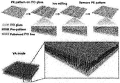
- FIG. 1 illustrates a method of manufacturing a transparent electrode according to the present invention and an alignment of a vertically aligned liquid crystal display device manufactured using the pattern.
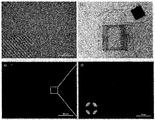
- FIG. 2 is a photoresist pattern (a) prepared on glass using ITO, a cell photograph prepared by VA mode, and a photograph attached with a polarizing plate (b). Polarization microscope photographs (c and d) of VA mode.
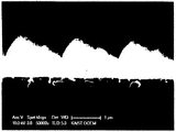
- FIG. 4 is a photograph of a transparent electrode having a U shape according to the present invention.
- FIG. 5 is a photograph of a transparent electrode of a standing form according to the present invention.
- a pre-pattern was formed on the glass on which ITO was deposited using a photoresist frame, and then ITO was attached to the side of the prepattern using ion milling, and the prepattern was removed to prepare a substrate on which the ITO pattern was formed.
- the present invention provides a method for forming a macro prepattern on a substrate to which a conductive material is applied; And (b) etching the substrate on which the macro prepattern is formed and depositing a conductive material on both sides of the macro prepattern.
- a method for manufacturing a conductive material comprising: (a) applying a conductive material onto a substrate on which a macro prepattern is formed; And (b) etching the substrate on which the macro prepattern is formed and depositing a conductive material on both sides of the macro prepattern.
- the thickness of the deposited conductive material is 1nm ⁇ 100 ⁇ m, the height is 10nm ⁇ 1000 ⁇ m, it may be characterized in that the interval between the deposited conductive material is 1 ⁇ 100 ⁇ m.
- the thickness is 1nm ⁇ 10 ⁇ m, the height is 10nm ⁇ 100 ⁇ m, the interval between the deposited conductive material is 1 ⁇ 50 ⁇ m, more preferably the thickness is 1nm ⁇ 100nm and the height is 200nm ⁇ 800nm, the deposited conductivity
- the spacing between the materials may be 1-10 ⁇ m.
- the macro prepattern may be formed by depositing a prepattern material on a substrate and performing a photolithography or imprinting process.
- the macro prepattern can be used without limitation as long as it forms a macro prepattern having a predetermined shape on the substrate because a conductive material is deposited on the side to form a transparent electrode.
- a photolithography or imprinting process is used. Can be.
- the conductive material is gold, platinum, silver, copper, aluminum, zinc oxide, chromium, indium tin oxide (ITO), nickel, iron, titanium, molybdenum, silicon, zinc oxide (zinc oxide) or titanium oxide It may be characterized in that (titanium oxide).
- the conductive material is deposited on the side of the macro prepattern by etching, and then the conductive material is applied to the substrate to form a macro prepattern, or the macro prepattern may be formed, and then the conductive material may be applied.
- the erected portion of the erected transparent electrode and the U-shaped transparent electrode preferably has an angle of 70 to 90 degrees with respect to the substrate, more preferably 80 to 90 degrees, most preferably 85 to 90 degrees Can have
- the conductive material may be used without limitation as long as the material can form a transparent electrode.
- it may be gold, platinum, silver, copper, aluminum, zinc oxide, chromium, or indium tin oxide (ITO), and more preferably indium tin oxide (ITO) may be used.
- step (c) removing the macro prepattern; and may be further included.
- the macro prepattern is generally removed to improve the transparency of the substrate on which the transparent electrode is formed. However, when the macro prepattern has a specific function, the macro prepattern may be used without being removed as necessary.
- the substrate may be selected from the group consisting of polyethylene terephthalate (polyehtylene terephthalate), polyacrylate (polyacrylate), polyethylene (polyethylene), quartz, glass, silicon, silicon oxide and mixtures thereof. And, preferably, glass can be used.
- the macro prepattern may be made of polystyrene, chitosan, polyvinylalcohol, polymethyl methacrylate (PMMA), photoresist or conductive polymer.
- the macro prepattern is formed in a predetermined shape by a lithography or an imprinting process, and a conductive material is deposited on the side by etching. In this case, the height and the spacing of the macro prepattern may be adjusted to adjust the height and the spacing of the deposited conductive material.
- the etching may be characterized in that it is performed by milling or sputtering.
- the conductive material applied to the substrate exposed between the macro prepatterns is deposited on both sidewalls of the macro prepattern by etching.
- the etching is preferably performed by milling or sputtering, and more preferably, may be performed by ion milling.
- the milling is performed by forming a plasma using a gas under a pressure of 0.001 mTorr to 10 mTorr, and then accelerating the plasma to 100 V to 700 V.
- the time is preferably 20 to 200 seconds, but is not limited thereto.
- the gas used for ion milling is preferably selected from the group consisting of argon, helium, nitrogen, oxygen, and mixtures thereof.
- the transparent electrodes manufactured by the above method face each other and the patterns are arranged in a vertical direction, and then a liquid crystal is injected between the arranged substrates to obtain a vertically aligned liquid crystal display device.
- the present invention relates to a method of manufacturing a vertical alignment liquid crystal display device comprising the step.
- the present invention includes the step of obtaining a vertically aligned liquid crystal display device by arranging the transparent electrodes prepared by the above method facing each other and the pattern is the same direction, and then injecting the liquid crystal between the arranged substrates It relates to a method of manufacturing a vertical alignment liquid crystal display device.
- the transparent electrode manufactured by the above method is formed perpendicular to one side of the substrate. After arranging two substrates such that the transparent electrodes face each other, a liquid crystal is injected between the substrates to manufacture a vertical alignment liquid crystal display device. In this case, the two substrates may be arranged such that two vertically formed transparent electrodes are arranged in the same direction or cross each other.
- a macroprepattern was fabricated using photoresist on the glass on which the ITO was deposited as shown in FIG. Finally, the macro prepattern was removed with a solvent, leaving only a 10 nm thick pattern. The width between the deposited ITO is 5um and the height is about 400 ⁇ 600nm.
- the transparent electrode fabricated in Example 1 with both sides the liquid crystal cells are assembled by assembling the liquid crystal cells so that the patterns look perpendicular to each other. As a result, a liquid crystal display of VA mode in which the liquid crystals stand vertically is produced.
- FIG. 2A a pattern is formed based on a free pattern on ITO glass
- FIG. 2B is a VA mode liquid crystal display made of ITO patterns.
- the small picture of Figure 2b shows a black screen with VA mode placed on both sides vertically.
- the line width is 5um and the height is about 800nm.
- the vertical alignment liquid crystal display device manufactured by the manufacturing method according to the present invention is almost completely black, and the vertical alignment of the liquid crystal is possible by a simple physical method without an alignment layer, which is useful for manufacturing high-performance displays.
Landscapes
- Physics & Mathematics (AREA)
- Nonlinear Science (AREA)
- Mathematical Physics (AREA)
- Chemical & Material Sciences (AREA)
- Crystallography & Structural Chemistry (AREA)
- General Physics & Mathematics (AREA)
- Optics & Photonics (AREA)
- Liquid Crystal (AREA)
Abstract
본 발명은 매크로 프리패턴이 형성된 기판을 에칭하여 프리패턴의 측면에 전도성 물질을 증착한 다음, 매크로 프리패턴을 제거하여 생성되는 투명전극의 제조방법과 상기 투명전극을 이용하는 수직 배향형 액정표시소자의 제조방법에 관한 것으로서, 본 발명에 따른 제조방법으로 제조된 수직배향형 액정표시소자는 검은색이 거의 완벽히 구현되며, 배향막 없이 간단한 물리적 방법만으로 액정의 수직배향이 가능하여 고성능의 디스플레이 제조에 유용하다.
Description
본 발명은 매크로 프리패턴을 이용한 투명전극 및 수직 배향형 액정표시소자의 제조방법에 관한 것으로, 더욱 상세하게는 매크로 프리패턴이 형성된 기판을 에칭하여 프리패턴의 측면에 전도성 물질을 증착한 다음, 매크로 프리패턴을 제거하여 생성되는 투명전극의 제조방법과 상기 투명전극을 이용하는 수직 배향형 액정표시소자의 제조방법에 관한 것이다.
액정표시장치 연구분야에 있어 액정을 배향막 없이 다양한 모드로 배향하는 것이 중요한 연구 분야이다. 투명전극 위에 새로운 배향막을 추가하지 않는 것이 큰 이슈이지만, 무배향막의 VA모드를 제작하는 연구는 기존에 많이 이루어지지 않은 연구분야이다. 완벽한 VA모드를 구현하기 위해 다양한 화학적 방법을 사용하고 있지만, 물리적인 방법만을 이용하여 VA모드를 구현하는 방법은 많지 않으며, 방법이 상당히 복잡한 단점이 있다.
액정 디스플레이 분야에서 수직 배향은 검은색을 거의 완벽히 구현할 수 있다는 장점이 있기 때문에 널리 사용되고 있다. 하지만, 기존의 폴리머를 사용할 경우, 오염, 정전기, 불필요한 에너지 소모, 고온공정 등 여러 가지 단점들이 있다. 이런 단점들을 극복하기 위해 무배향막 디스플레이 또한 연구가 되고 있다.
무배향막 디스플레이를 위해 투명전극인 ITO를 패터닝하여 물리적으로 액정을 배향하는 방법이 제안되고 있다. 하지만, 수직배향은 굉장히 어려운 분야로, 깔끔한 검은색을 얻기 쉽지 않고, 그 방법조차 굉장히 복잡하다. 따라서, 간단한 방법으로 수직배향 액정표시장치를 얻는 방법이 필요하다.
대한민국 등록특허 10-125154호에는 나노구조 패턴이 형성된 투명전극 및 이를 이용한 수직배향형 액정표시소자에 관하여 기재하고 있다. 이 발명에서는 ITO를 이용하여 격자형상의 패턴을 제작하였지만, 복잡하고 많은 단계를 거치는 공정을 사용하며, 깔끔한 검은색을 얻기 힘들다는 단점을 가진다.
이에, 본 발명자들은 상기 문제점을 해결하기 위하여 예의 노력한 결과, 매크로 패턴을 이용한 투명전극 제조방법 및 이를 이용한 수직 배향형 액정표시소자의 제조방법을 개발하였으며, 상기 수직 배향형 액정표시소자가 VA모드에서 배향막 없이 검은색을 거의 완벽히 구현 가능하다는 것을 확인하고, 본 발명을 완성하게 되었다.
발명의 요약
본 발명의 목적은 매크로 프리패턴을 이용한 투명전극의 제조방법을 제공하는데 있다.
본 발명의 다른 목적은 상기 투명 전극을 이용한 수직 배향형 액정표시소자의 제조방법을 제공하는데 있다.
상기 목적을 달성하기 위하여, 본 발명은 (a) 전도성 물질이 도포된 기판 위에 매크로 프리패턴을 형성하는 단계; 및 (b) 상기 매크로 프리패턴이 형성된 기판을 에칭하여 전도성 물질을 매크로 프리패턴의 양 측면에 증착하는 단계를 포함하는 매크로 프리패턴을 이용한 투명전극의 제조방법을 제공한다.
본 발명은 또한, (a) 매크로 프리패턴이 형성된 기판 위에 전도성 물질을 도포하는 단계; 및 (b) 상기 매크로 프리패턴이 형성된 기판을 에칭하여 전도성 물질을 매크로 프리패턴의 양 측면에 증착하는 단계를 포함하는 매크로 프리패턴을 이용한 투명전극의 제조방법을 제공한다.
본 발명은 또한, 상기 방법으로 제조된 투명전극이 서로 마주보게 하고 패턴이 수직방향이 되도록 배열한 다음, 상기 배열된 기판 사이로 액정을 주입하여 수직배향형 액정표시소자를 수득하는 단계를 포함하는 수직배향형 액정표시소자의 제조방법을 제공한다.
본 발명은 또한, 상기 방법으로 제조된 투명전극이 마주보게 배열하고 패턴이 같은 방향이 되도록 다음, 상기 배열된 기판 사이로 액정을 주입하여 수직배향형 액정표시소자를 수득하는 단계를 포함하는 수직배향형 액정표시소자의 제조방법을 제공한다.
도 1은 본 발명에 의한 투명전극의 제조방법과 상기 패턴을 이용하여 제조되는 수직 배향형 액정표시장치의 배향모습을 도시한 것이다.
도 2는 ITO를 이용하여 유리 위에 제작된 포토레지스트 패턴(a)과 VA모드를 제작한 셀 사진 및 편광판을 붙인 사진(b). VA 모드의 편광현미경 사진(c와 d)이다.
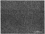
도 3은 ITO 패턴의 광학현미경 사진이다.
도 4는 본 발명에 의한 U형상을 가지는 투명전극의 사진이다.
도 5는 본 발명에 의한 세워진 형태의 투명전극의 사진이다.
발명의 상세한 설명 및 구체적인
구현예
다른 식으로 정의되지 않는 한, 본 명세서에서 사용된 모든 기술적 및 과학적 용어들은 본 발명이 속하는 기술 분야에서 숙련된 전문가에 의해서 통상적으로 이해되는 것과 동일한 의미를 가진다. 일반적으로, 본 명세서에서 사용된 명명법은 본 기술 분야에서 잘 알려져 있고 통상적으로 사용되는 것이다.
본 발명에서는, ITO가 증착된 유리 위에 포토레지스트틀 이용하여 프리패턴을 형성한 다음, 이온밀링을 이용하여 프리패턴의 측면에 ITO를 부착하고 프리패턴을 제거하여 ITO패턴이 형성된 기판을 제작하였으며, 상기 기판을 이용하여 VA모드의 액정표시장치를 제작한 결과, 검은색이 거의 완벽이 구현되며, 배향막 없이 간단한 물리적 방법만으로 액정의 수직배향이 가능한 것을 확인할 수 있었다.
따라서, 본 발명은 일 관점에서, (a) 전도성 물질이 도포된 기판위에 매크로 프리패턴을 형성하는 단계; 및 (b) 상기 매크로 프리패턴이 형성된 기판을 에칭하여 전도성 물질을 매크로 프리패턴의 양 측면에 증착하는 단계를 포함하는 매크로 프리패턴을 이용한 투명전극의 제조방법에 관한 것이다.
본 발명은 다른 관점에서, (a) 매크로 프리패턴이 형성된 기판 위에 전도성 물질을 도포하는 단계; 및 (b) 상기 매크로 프리패턴이 형성된 기판을 에칭하여 전도성 물질을 매크로 프리패턴의 양 측면에 증착하는 단계를 포함하는 매크로 프리패턴을 이용한 투명전극의 제조방법에 관한 것이다.
본 발명에 있어서, 상기 증착된 전도성 물질의 두께는 1nm~100㎛이고 높이는 10nm~1000㎛이며, 증착된 전도성 물질 사이의 간격이 1~100㎛인 것을 특징으로 할 수 있다. 바람직하게는 두께는 1nm~10㎛이고 높이는 10nm~100㎛이며, 증착된 전도성 물질 사이의 간격이 1~50㎛이며, 더욱 바람직하게는 두께는 1nm~100nm이고 높이는 200nm~800nm이며, 증착된 전도성 물질 사이의 간격이 1~10㎛일 수 있다.
본 발명에 있어서, 상기 매크로 프리패턴은 기판 상에 프리패턴 물질을 증착시키고 포토리소그래피 또는 임프린팅 공정을 수행하여 형성하는 것을 특징으로 할 수 있다. 매크로 프리패턴은 전도성 물질이 측면에 증착되어 투명전극을 형성하는 데 사용되므로 기판위에 일정한 모양을 가지는 매크로 프리패턴을 형성하는 공정이면 제한 없이 사용가능 하지만, 바람직하게는 포토리소그래피 또는 임프린팅 공정을 사용할 수 있다.
본 발명에 있어서, 상기 전도성 물질은 금, 백금, 은, 구리, 알루미늄, 징크옥사이드, 크롬, 인듐 틴 옥사이드(ITO), 니켈, 철, 티타늄, 몰리브덴, 실리콘, 징크옥사이드(zinc oxide) 또는 티타늄 옥사이드(titanium oxide)인 것을 특징으로 할 수 있다. 전도성 물질은 에칭에 의하여 매크로 프리패턴의 측면에 증착되며, 기판에 전도성 물질이 도포된 다음 매크로 프리패턴을 형성하거나, 매크로 프리패턴을 형성한 다음 전도성 물질을 도포 가능하다. 이때 전도성 물질을 매크로 프리패턴의 형성 전에 도포하는 경우 매크로 프리패턴의 하부와 기판 사이에 전도성 물질이 존재하므로 애칭 이후, 단면이 U형상을 가지는 투명전극을 수득할 수 있으며(도 4), 매크로 프리패턴의 형성이 후전도성 물질을 도포하는 경우 매크로 프리패턴의 측면에 증착된 전도성 물질 이외의 전도성 물질은 전부 제거되므로, 새워진 형태의 투명전극을 수득할 수 있다(도 5). 또한 세워진 형태의 투명전극 및 U자형 투명전극의 세워진 부분은 기판에 대하여 70~90°의 각도를 가지는 것이 바람직하며, 더욱 바람직하게는 80~90°, 가장 바람직하게는 85~90°의 각도를 가질 수 있다.
또한 상기 전도성 물질은 투명전극이 형성 가능한 물질이면 제한 없이 사용 가능하지만. 바람직하게는 금, 백금, 은, 구리, 알루미늄, 징크옥사이드, 크롬, 또는 인듐 틴 옥사이드(ITO)일 수 있으며, 더욱 바람직하게는 인듐 틴 옥사이드(ITO)를 사용 가능하다.
본 발명에 있어서, 상기 (b)단계 이후; (c) 매크로 프리패턴을 제거하는 단계;를 추가로 포함하는 것을 특징으로 할 수 있다. 상기 매크로 프리패턴은 일반적으로 제거하여 투명전극이 형성된 기판의 투명도를 향상시키지만, 매크로 프리패턴이 특정한 기능을 가지는 경우 필요에 따라 제거하지 않고 사용할 수 있다.
본 발명에 있어서, 상기 기판은 폴리에틸렌테레프탈레이트(polyehtyleneterephthalate), 폴리아크릴레이트(polyacrylate), 폴리에틸렌(polyethylene), 석영, 유리, 실리콘, 실리콘 산화물 및 이들의 혼합물로 구성된 군에서 선택되는 것을 특징으로 할 수 있으며, 바람직하게는 유리를 사용할 수 있다.
본 발명에 있어서, 상기 메크로 프리패턴은 폴리스타일렌, 키토산, 폴리비닐알코올(polyvinylalcohol), 폴리메틸메타아크릴레이트(PMMA), 포토레지스트 화합물(photoresist) 또는 전도성 고분자로 제작되는 것을 특징으로 할 수 있다. 매크로 프리패턴은 리소그래피 또는 임프린팅 공정에 의하여 일정 모양으로 형성되고, 측면에 에칭에 의하여 전도성 물질이 증착된다. 이때, 매크로 프리패턴의 높이와 간격을 조절하여 증착되는 전도성 물질의 높이와 간격을 조절할 수 있다.
본 발명에 있어서, 상기 에칭은 밀링 또는 스퍼터링으로 수행되는 것을 특징으로 할 수 있다. 매크로 프리패턴 사이로 노출된 기판에 도포된 전도성 물질은 에칭에 의하여 매크로 프리패턴의 양측 벽면에 증착된다. 이때 에칭은 밀링 또는 스퍼터링으로 수행하는 것이 바람직하며, 더욱 바람직하게는 이온밀링으로 수행할 수 있다. 상기 밀링은 0.001mTorr~10mTorr의 압력하에서 기체를 이용하여 플라즈마를 형성한 다음 상기 플라즈마를 100V~700V로 가속화하여 수행되며, 시간은 20~200초인 것이 바람직하지만 이에 제한되는 것은 아니다. 또한 상기 이온 밀링에 사용되는 기체는 아르곤, 헬륨, 질소, 산소 및 이들의 혼합기체로 구성된 군에서 선택되는 것이 바람직하다.
한편, 상기의 방법으로 제조된 투명전극을 이용하여 수직배향형 액정 표시소자를 제작하는 경우, 검은색이 거의 완벽하게 구현될 것으로 예측하였다.
따라서, 본 발명은 또 다른 관점에서, 상기 방법으로 제조된 투명전극이 서로 마주보게 하고 패턴이 수직방향이 되도록 배열한 다음, 상기 배열된 기판 사이로 액정을 주입하여 수직배향형 액정표시소자를 수득하는 단계를 포함하는 수직배향형 액정표시소자의 제조방법에 관한 것이다.
또한 본 발명은 또 다른 관점에서, 상기 방법으로 제조된 투명전극이 마주보게 배열하고 패턴이 같은 방향이 되도록 다음, 상기 배열된 기판 사이로 액정을 주입하여 수직배향형 액정표시소자를 수득하는 단계를 포함하는 수직배향형 액정표시소자의 제조방법에 관한 것이다.
상기 방법으로 제조된 투명전극은 기판의 일측면에 수직으로 형성된다. 이러한 기판 두 장을 투명전극이 마주보게 배열한 다음, 기판의 사이에 액정을 주입하여 수직배향형 액정표시소자를 제작할 수 있다. 이때 두 장의 기판은 마주보는 두 개의 수직으로 형성된 투명전극이 동일한 방향으로 배열하거나 서로 교차되도록 배열할 수 있다.
실시예
이하, 실시예를 통하여 본 발명을 더욱 상세히 설명하고자 한다. 이들 실시예는 오로지 본 발명을 예시하기 위한 것으로, 본 발명의 범위가 이들 실시예에 의해 제한되는 것으로 해석되지 않는 것은 당업계에서 통상의 지식을 가진 자에게 있어서 자명할 것이다.
실시예 1: 매크로 프리패턴을 이용한 투명 전극의 제작
도 1과 같이 ITO가 증착된 유리 위에 포토레지스트를 이용하여 매크로 프리패턴을 제작하고, 이온밀링을 통해 매크로 프리패턴 벽면에 ITO를 증착하여 10nm 두께로 만들었다. 마지막으로 매크로 프리패턴을 용매로 제거하여 10nm 두께의 패턴만 남겼다. 증착된 ITO 사이의 폭은 5um이며 높이는 약 400~600nm 정도로 만들었다. 프리패턴을 제작할 때, 포토레지스트로 제작을 해도 되지만, 임프린팅 작업으로 프리패턴을 제작해도 무방하다.
실시예 2: 상기 투명 전극을 이용한 수직배향형 액정표시소자의 제작
도 1의 하단부에 나타난 바와 같이, 실시예 1에서 제작된 투명전극을 양면으로 하여, 패턴이 서로 수직으로 바라보게 액정 셀을 조립하여 액정을 주입한다. 그 결과, 액정이 수직으로 서 있는 VA 모드의 액정디스플레이가 제작된다.
도 2a와 같이 ITO 유리 위에 있는 프리 패턴을 기반으로 패턴을 만들며, 도 2b는 ITO 패턴으로 만든 VA 모드 액정디스플레이다. 도 2b의 작은 사진은 편광판을 수직으로 양면에 넣어 VA 모드가 보이는 검은 화면을 보여준다. 도 2c와 도 2d는 POM 사진으로, 액정분자가 수직으로 서 있는 것을 보여주는 사진이다. 도 2d의 코노스코피(conoscopy)를 보면 정확히 VA 모드임을 알 수 있다. 패턴의 높이/셀 갭 = 0.5 이상일 경우, VA 모드가 나오게 되며, 선폭은 넓을수록 수직배향이 잘 된다.
도 3은 광학현미경으로 관찰한 ITO 패턴이다. 선폭은 5um이며, 높이는 800nm 정도이다.
본 발명에 따른 제조방법으로 제조된 수직배향형 액정표시소자는 검은색이 거의 완벽히 구현되며, 배향막 없이 간단한 물리적 방법만으로 액정의 수직배향이 가능하여 고성능의 디스플레이 제조에 유용하다.
이상으로 본 발명의 특정한 부분을 상세히 기술하였는바, 당업계의 통상의 지식을 가진 자에게 있어서, 이러한 구체적 기술은 단지 바람직한 실시양태일 뿐이며, 이에 의해 본 발명의 범위가 제한되는 것이 아닌 점은 명백할 것이다. 따라서 본 발명의 실질적인 범위는 첨부된 청구항들과 그것들의 등가물에 의하여 정의된다고 할 것이다.
Claims (11)
- 다음 단계를 포함하는 매크로 프리패턴을 이용한 투명전극의 제조방법:(a) 전도성 물질이 도포된 기판위에 매크로 프리패턴을 형성하는 단계; 및(b) 상기 매크로 프리패턴이 형성된 기판을 에칭하여 전도성 물질을 매크로 프리패턴의 양 측면에 증착하는 단계.
- 다음 단계를 포함하는 매크로 프리패턴을 이용한 투명전극의 제조방법:(a) 매크로 프리패턴이 형성된 기판 위에 전도성 물질을 도포하는 단계; 및(b) 상기 매크로 프리패턴이 형성된 기판을 에칭하여 전도성 물질을 매크로 프리패턴의 양 측면에 증착하는 단계.
- 제1항 또는 제2항에 있어서, 상기 (b)단계 이후;(c) 매크로 프리패턴을 제거하는 단계;를 추가로 포함하는 것을 특징으로 하는 투명전극의 제조방법.
- 제1항 또는 제2항에 있어서, 상기 증착된 전도성 물질의 두께는 1nm~100㎛이고 높이는 10nm~1000㎛이며, 증착된 전도성 물질의 간격이 1~100㎛인 것을 특징으로 하는 투명 전극의 제조방법.
- 제1항 또는 제2항에 있어서, 상기 매크로 프리패턴은 기판 상에 프리패턴 물질을 증착시키고 리소그래피 또는 임프린팅 공정을 수행하여 형성하는 것을 특징으로 하는 투명전극의 제조방법.
- 제1항 또는 제2항에 있어서, 상기 에칭은 밀링 또는 스퍼터링으로 수행되는 것을 특징으로 하는 투명전극의 제조방법.
- 제6항에 있어서, 상기 밀링은 0.001mTorr~10mTorr의 압력하에서 기체를 이용하여 플라즈마를 형성한 다음 상기 플라즈마를 100V~700V로 가속화하여 수행되는 것을 특징으로 하는 투명전극의 제조방법.
- 제1항 또는 제2항의 방법으로 제조된 투명전극이 서로 마주보게 하고 패턴이 수직방향이 되도록 배열한 다음, 상기 배열된 기판 사이로 액정을 주입하여 수직배향형 액정표시소자를 수득하는 단계를 포함하는 수직배향형 액정표시소자의 제조방법.
- 제1항 또는 제2항의 방법으로 제조된 투명전극이 마주보게 배열하고 패턴이 같은 방향이 되도록 다음, 상기 배열된 기판 사이로 액정을 주입하여 수직배향형 액정표시소자를 수득하는 단계를 포함하는 수직배향형 액정표시소자의 제조방법.
- 제3항의 방법으로 제조된 투명전극이 서로 마주보게 하고 패턴이 수직방향이 되도록 배열한 다음, 상기 배열된 기판 사이로 액정을 주입하여 수직배향형 액정표시소자를 수득하는 단계를 포함하는 수직배향형 액정표시소자의 제조방법.
- 제3항의 방법으로 제조된 투명전극이 마주보게 배열하고 패턴이 같은 방향이 되도록 다음, 상기 배열된 기판 사이로 액정을 주입하여 수직배향형 액정표시소자를 수득하는 단계를 포함하는 수직배향형 액정표시소자의 제조방법.
Applications Claiming Priority (4)
| Application Number | Priority Date | Filing Date | Title |
|---|---|---|---|
| KR20150021730 | 2015-02-12 | ||
| KR10-2015-0021730 | 2015-02-12 | ||
| KR10-2015-0125410 | 2015-09-04 | ||
| KR1020150125410A KR102362199B1 (ko) | 2015-02-12 | 2015-09-04 | 매크로 프리패턴을 이용한 투명전극 및 수직 배향형 액정표시소자의 제조방법 |
Publications (1)
| Publication Number | Publication Date |
|---|---|
| WO2016129782A1 true WO2016129782A1 (ko) | 2016-08-18 |
Family
ID=56615417
Family Applications (1)
| Application Number | Title | Priority Date | Filing Date |
|---|---|---|---|
| PCT/KR2015/012377 Ceased WO2016129782A1 (ko) | 2015-02-12 | 2015-11-18 | 매크로 프리패턴을 이용한 투명전극 및 수직 배향형 액정표시소자의 제조방법 |
Country Status (1)
| Country | Link |
|---|---|
| WO (1) | WO2016129782A1 (ko) |
Citations (5)
| Publication number | Priority date | Publication date | Assignee | Title |
|---|---|---|---|---|
| KR100767902B1 (ko) * | 2000-12-06 | 2007-10-17 | 닛토덴코 가부시키가이샤 | 호메오트로픽 배향 액정 필름의 제조방법, 호메오트로픽배향 액정성 조성물 및 호메오트로픽 배향 액정 필름 |
| KR101231898B1 (ko) * | 2011-06-20 | 2013-02-08 | 한국과학기술원 | 나노구조 패턴이 형성된 투명전극 및 그 제조방법 |
| WO2013094957A1 (ko) * | 2011-12-19 | 2013-06-27 | 성균관대학교 산학협력단 | 액정 배향 방법, 액정 소자, 액정 표시 장치, 액정 표시 장치 제조 방법 및 액정 셀 기판 제조 방법 |
| KR101356074B1 (ko) * | 2012-02-09 | 2014-01-28 | 한국과학기술원 | 터치패널용 전극의 제조방법 |
| KR20150009864A (ko) * | 2013-07-17 | 2015-01-27 | 동우 화인켐 주식회사 | 위상차 필름 및 이를 구비하는 화상 표시 장치 |
-
2015
- 2015-11-18 WO PCT/KR2015/012377 patent/WO2016129782A1/ko not_active Ceased
Patent Citations (5)
| Publication number | Priority date | Publication date | Assignee | Title |
|---|---|---|---|---|
| KR100767902B1 (ko) * | 2000-12-06 | 2007-10-17 | 닛토덴코 가부시키가이샤 | 호메오트로픽 배향 액정 필름의 제조방법, 호메오트로픽배향 액정성 조성물 및 호메오트로픽 배향 액정 필름 |
| KR101231898B1 (ko) * | 2011-06-20 | 2013-02-08 | 한국과학기술원 | 나노구조 패턴이 형성된 투명전극 및 그 제조방법 |
| WO2013094957A1 (ko) * | 2011-12-19 | 2013-06-27 | 성균관대학교 산학협력단 | 액정 배향 방법, 액정 소자, 액정 표시 장치, 액정 표시 장치 제조 방법 및 액정 셀 기판 제조 방법 |
| KR101356074B1 (ko) * | 2012-02-09 | 2014-01-28 | 한국과학기술원 | 터치패널용 전극의 제조방법 |
| KR20150009864A (ko) * | 2013-07-17 | 2015-01-27 | 동우 화인켐 주식회사 | 위상차 필름 및 이를 구비하는 화상 표시 장치 |
Similar Documents
| Publication | Publication Date | Title |
|---|---|---|
| CN202563217U (zh) | 一种液晶面板以及显示装置 | |
| US7799392B2 (en) | Color filter substrate and fabricating method thereof | |
| EP2713204A1 (en) | Electrochromic color filter substrate, method of fabricating the same, and LCD panel comprising the same | |
| CN104091761B (zh) | 一种图案化薄膜的制备方法、显示基板及显示装置 | |
| CN104849906B (zh) | 偏光片及其制造方法、显示装置 | |
| CN106597728A (zh) | 彩膜基板及液晶显示面板 | |
| WO2012177040A2 (ko) | 나노구조 패턴이 형성된 투명전극 및 그 제조방법 | |
| CN105954943A (zh) | 显示面板、应用其的显示装置及显示面板的制造方法 | |
| CN108983515B (zh) | 一种液晶显示器件及其制备方法和显示装置 | |
| WO2014173140A1 (zh) | 彩色滤光片、彩色滤光片制作方法和显示装置 | |
| CN105974683A (zh) | 液晶显示面板及其制作方法 | |
| WO2013159538A1 (zh) | 有机薄膜晶体管阵列基板及其制备方法以及显示装置 | |
| US20140144875A1 (en) | Method for Manufacturing Reflective Polarizer | |
| KR101251541B1 (ko) | 나노구조 패턴이 형성된 투명전극 및 이를 이용한 수직배향형 액정표시소자 | |
| CN106783893A (zh) | 显示基板及其制作方法、显示装置 | |
| KR102362199B1 (ko) | 매크로 프리패턴을 이용한 투명전극 및 수직 배향형 액정표시소자의 제조방법 | |
| KR20170112310A (ko) | 투명 전극 구조체 및 이의 제조방법 | |
| WO2016129782A1 (ko) | 매크로 프리패턴을 이용한 투명전극 및 수직 배향형 액정표시소자의 제조방법 | |
| CN107632438A (zh) | 一种显示面板的制备方法、显示面板及显示装置 | |
| JP6304952B2 (ja) | 液晶ディスプレイパネル及びその製造方法、並びに液晶表示装置 | |
| CN101750792B (zh) | 共平面开关模式液晶显示装置的滤色器基板及其制造方法 | |
| CN106483720B (zh) | 显示面板及其制造方法 | |
| WO2016078117A1 (zh) | 显示面板及显示装置 | |
| CN103489873A (zh) | 阵列基板及其制作方法、显示装置 | |
| CN114253024B (zh) | 彩膜基板的制备方法及液晶显示面板的制备方法 |
Legal Events
| Date | Code | Title | Description |
|---|---|---|---|
| 121 | Ep: the epo has been informed by wipo that ep was designated in this application |
Ref document number: 15882144 Country of ref document: EP Kind code of ref document: A1 |
|
| NENP | Non-entry into the national phase |
Ref country code: DE |
|
| 122 | Ep: pct application non-entry in european phase |
Ref document number: 15882144 Country of ref document: EP Kind code of ref document: A1 |