WO2016129619A1 - 導波管、無線電力伝送システム、および無線通信システム - Google Patents
導波管、無線電力伝送システム、および無線通信システム Download PDFInfo
- Publication number
- WO2016129619A1 WO2016129619A1 PCT/JP2016/053894 JP2016053894W WO2016129619A1 WO 2016129619 A1 WO2016129619 A1 WO 2016129619A1 JP 2016053894 W JP2016053894 W JP 2016053894W WO 2016129619 A1 WO2016129619 A1 WO 2016129619A1
- Authority
- WO
- WIPO (PCT)
- Prior art keywords
- waveguide
- dielectric
- electromagnetic wave
- wireless
- coated
- Prior art date
- Legal status (The legal status is an assumption and is not a legal conclusion. Google has not performed a legal analysis and makes no representation as to the accuracy of the status listed.)
- Ceased
Links
Images




Classifications
-
- H—ELECTRICITY
- H01—ELECTRIC ELEMENTS
- H01P—WAVEGUIDES; RESONATORS, LINES, OR OTHER DEVICES OF THE WAVEGUIDE TYPE
- H01P3/00—Waveguides; Transmission lines of the waveguide type
- H01P3/12—Hollow waveguides
-
- H—ELECTRICITY
- H02—GENERATION; CONVERSION OR DISTRIBUTION OF ELECTRIC POWER
- H02J—ELECTRIC POWER NETWORKS; CIRCUIT ARRANGEMENTS OR SYSTEMS FOR SUPPLYING OR DISTRIBUTING ELECTRIC POWER; SYSTEMS FOR STORING ELECTRIC ENERGY
- H02J50/00—Circuit arrangements or systems for wireless supply or distribution of electric power
-
- H—ELECTRICITY
- H01—ELECTRIC ELEMENTS
- H01P—WAVEGUIDES; RESONATORS, LINES, OR OTHER DEVICES OF THE WAVEGUIDE TYPE
- H01P11/00—Apparatus or processes specially adapted for manufacturing waveguides or resonators, lines, or other devices of the waveguide type
-
- H—ELECTRICITY
- H01—ELECTRIC ELEMENTS
- H01P—WAVEGUIDES; RESONATORS, LINES, OR OTHER DEVICES OF THE WAVEGUIDE TYPE
- H01P3/00—Waveguides; Transmission lines of the waveguide type
- H01P3/12—Hollow waveguides
- H01P3/127—Hollow waveguides with a circular, elliptic, or parabolic cross-section
-
- H—ELECTRICITY
- H01—ELECTRIC ELEMENTS
- H01P—WAVEGUIDES; RESONATORS, LINES, OR OTHER DEVICES OF THE WAVEGUIDE TYPE
- H01P3/00—Waveguides; Transmission lines of the waveguide type
- H01P3/12—Hollow waveguides
- H01P3/14—Hollow waveguides flexible
Definitions
- Some embodiments of the present invention relate to a waveguide for transmitting power or performing wireless communication, and a wireless power transmission system and a wireless communication system including the waveguide.
- waveguides are mainly used for transmission of electromagnetic waves such as microwaves or millimeter waves.
- an in-vehicle communication system using a waveguide has been proposed (see Patent Document 1).
- some embodiments of the present invention have an object to provide a waveguide considering the frequency and propagation mode of an electromagnetic wave to be transmitted, and a wireless power transmission system and a wireless communication system including the waveguide. To do.
- the waveguide includes a cylindrical body made of a cylindrical dielectric and a covering body made of a conductor covering an outer peripheral side surface of the cylindrical body, and is a waveguide for propagating electromagnetic waves,
- the distance between the inner surfaces of the covering in the orthogonal direction orthogonal to the direction of the electric field vector of the electromagnetic wave It is characterized by being smaller than the standard dimension by an amount determined by the thickness of the dielectric and the dielectric constant of the dielectric in the orthogonal direction.
- the waveguide has a structure in which the side surface of the cylindrical body made of a cylindrical dielectric is covered with a covering made of a conductor, and thus is lighter and more flexible than a metal waveguide.
- the waveguide according to some embodiments of the present invention has a structure in which the outer peripheral side surface is coated with a conductor, and is easier to manufacture than coating the inner peripheral side surface with a conductor.
- the inner peripheral surface side where electromagnetic waves are transmitted among conductors is covered with a dielectric and is not directly exposed to electromagnetic waves, durability is high.
- the substantial distance between the inner surfaces of the covering as viewed from the electromagnetic wave is as described above. It becomes larger than the distance between the inner surfaces of the actual covering. More quantitatively, the substantial distance between the inner surfaces of the covering body as viewed from the electromagnetic wave is greater than the actual distance between the inner surfaces of the covering body and the thickness of the dielectric body in the orthogonal direction and the dielectric body. Increases by an amount determined by the dielectric constant.
- the waveguide in some embodiments of the present invention has a predetermined waveguide standard dimension at the frequency of the transmitted electromagnetic wave, wherein the distance D between the inner surfaces of the covering corresponds to the substantial distance D ′. It is set to the dimension corresponding to. For example, when the cross-sectional shape is circular, the distance D is set so that the substantial distance D ′ corresponds to the frequency of the electromagnetic wave transmitted in the TE11 mode in the EIAJ standard circular waveguide. Therefore, the waveguide in some embodiments of the present invention is a waveguide that takes into account the frequency and propagation mode of the electromagnetic wave to be transmitted.
- the waveguide according to some embodiments of the present invention is such that the distance between the inner surfaces of the covering is in the orthogonal direction rather than the standard dimension of the prescribed waveguide corresponding to the frequency of the electromagnetic wave. It is reduced by an amount determined by the thickness of the dielectric and the dielectric constant of the dielectric, and the frequency and propagation mode of the electromagnetic wave to be transmitted are taken into consideration.
- the present invention it is possible to realize a waveguide taking into account the frequency and propagation mode of an electromagnetic wave to be transmitted, and a wireless power transmission system and a wireless communication system including the waveguide.
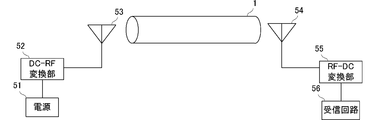
- FIG. 1 is a schematic block diagram showing a configuration of a wireless power transmission system including a waveguide according to the present invention.
- 2A is a perspective view of the waveguide 1
- FIG. 2B is a cross-sectional view of the waveguide 1 orthogonal to the transmission direction of the electromagnetic wave propagating through the waveguide 1.
- FIG. 2C is a diagram showing the direction of the electric field vector in the cross-sectional view.
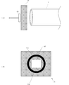
- 3A and 3B are schematic views showing the structure of the fixing jig 71 that connects the waveguide 1 and the transmission antenna 53.
- FIG. FIG. 4A and FIG. 4B are diagrams illustrating ports provided in part of the side surface of the waveguide 1.
- 5A, 5 ⁇ / b> B, and 5 ⁇ / b> C are diagrams illustrating ports provided in part of the side surface of the waveguide 1.
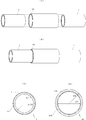
- 6 (A), 6 (B), 6 (C), 6 (D), 6 (E), and 6 (F) are diagrams showing modifications of the cross-sectional shape of the waveguide. is there. 7A, 7B, 7C, and 7D, the waveguide 1 and the inner peripheral side surface of the dielectric (cylindrical body) are conductors (covered bodies). It is a figure which shows the structure in the case of combining the covered waveguide 1A.
- FIG. 8 is a schematic block diagram showing the configuration of the wireless communication system.
- FIG. 1 is a schematic block diagram showing a configuration of a wireless power transmission system including a waveguide according to the present invention.
- the wireless power transmission system includes a power source 51, a DC-RF conversion unit 52, a transmission antenna 53, a waveguide 1, a reception antenna 54, an RF-DC conversion unit 55, and a reception circuit 56.
- the wireless power transmission system is installed, for example, in an automobile and is used to supply power from a battery to various electric devices.
- the power source 51 is, for example, a battery installed in an automobile.
- the DC-RF converter 52 converts the DC power extracted from the power supply 51 into a high-frequency signal (for example, 5.8 GHz) having a predetermined frequency.
- the transmission antenna 53 is, for example, a patch antenna, and radiates electromagnetic waves (microwaves) based on a high frequency signal input from the DC-RF conversion unit 52.
- the microwave radiated from the transmitting antenna 53 is coupled with the waveguide 1 and transmitted in a predetermined propagation mode.
- the receiving antenna 54 receives the electromagnetic wave transmitted through the waveguide 1.
- the RF-DC converter 55 converts the electromagnetic wave received by the receiving antenna 54 into DC power.
- the receiving circuit 56 corresponds to various electric devices installed in the automobile, and receives DC power from the RF-DC converter 55.
- FIG. 2A is a perspective view of the waveguide 1
- FIG. 2B is a cross-sectional view of the waveguide 1 orthogonal to the transmission direction of the electromagnetic wave propagating through the waveguide 1.
- FIG. 2C is a diagram showing the direction of the electric field vector in the cross-sectional view.
- the waveguide 1 includes a cylindrical body made of a cylindrical dielectric 21 and a covering made of a conductor 11 that covers the outer peripheral side surface of the cylindrical body.
- the dielectric 21 has a cylindrical shape, for example, and is made of, for example, ABS resin (acrylonitrile / butadiene / styrene copolymer).
- ABS resin acrylonitrile / butadiene / styrene copolymer
- the conductor 11 consists of a thin film of copper, for example, it is not limited to this, You may consist of other conductors, such as aluminum.
- the conductor (covered body) 11 is coated on the outer peripheral side surface of the dielectric (tubular body) 21 by, for example, plating or vapor deposition.
- the conductor 11 and the dielectric 21 may be made of a material having transparency that allows the inside of the waveguide 1 to be visually recognized from the outside. When a material having transparency is used, it is possible to confirm whether or not a foreign substance has entered the inside of the waveguide 1 without having to disassemble the waveguide 1.
- the waveguide 1 transmits an electromagnetic wave having a predetermined frequency (for example, a microwave of 5.8 GHz) in a tube axis direction in a predetermined propagation mode (for example, the TE11 mode).
- a predetermined frequency for example, a microwave of 5.8 GHz
- a predetermined propagation mode for example, the TE11 mode.
- the outer diameter ⁇ 1 corresponding to the distance D between the inner surfaces of the covering in the direction orthogonal to the direction of the electric field vector of the electromagnetic wave
- the inner diameter ⁇ 2 are set.
- the thickness of the conductor 11 is, for example, 1 ⁇ m.
- the skin depth ⁇ which is the distance at which the electromagnetic wave incident on the material attenuates to 1 / e ( ⁇ 8.7 dB), is ⁇ 0.8 ⁇ m. Therefore, the thickness of the conductor 11 is sufficient. However, the thickness of the conductor 11 may be further increased.
- a cutoff frequency fc of a TE11 mode which is a fundamental mode, can be expressed by the following formula 1 (where v0 is a radio wave transmission speed [m / s] in a vacuum) And ⁇ is the tube diameter [m]).
- the tube diameter ⁇ corresponds to the inner diameter of the conductor 11 and corresponds to the outer diameter ⁇ 1 (distance D) of the dielectric 21.
- the dielectric 21 is disposed inside the conductor 11. Since the wavelength of the electromagnetic wave is shortened when passing through the dielectric 21, the inner diameter is increased when viewed from the electromagnetic wave. That is, the substantial outer diameter ⁇ ′ viewed from the electromagnetic wave (the substantial distance D ′ between the inner surfaces of the covering in a straight line that is orthogonal to the direction of the electric field vector of the electromagnetic wave and passes through the center) is the tube diameter ⁇ . It becomes larger than (distance D between the inner surfaces of the covering).
- the substantial outer diameter ⁇ ′ (D ′) viewed from the electromagnetic wave is greater than the tube diameter ⁇ (D), and the thickness r of the dielectric 21 in the orthogonal direction perpendicular to the direction of the electric field vector of the electromagnetic wave. And an amount determined by the dielectric constant ⁇ of the dielectric 21 (for example, 2r ⁇ ).
- the cutoff frequency fc of the TE11 mode corresponding to the standard inner diameter 47.35 mm is 3.71 GHz. That is, it can be said that the outer diameter ⁇ 1 of the dielectric 11 corresponds to the size of the standard waveguide at the cutoff frequency of 3.71 GHz. Therefore, it can be said that the waveguide 1 can transmit an electromagnetic wave of 5.8 GHz in the TE11 mode.
- the propagation characteristic of the waveguide 1 having the above structure is ⁇ 0.245 dB / m in the simulation and ⁇ 0.72 dB / m in the experiment. Therefore, the waveguide 1 can transmit an electromagnetic wave of 5.8 GHz.
- the main material of the waveguide 1 as described above is a dielectric, it is extremely lightweight compared to a general metal waveguide.
- the weight of a general metal waveguide is 1 kg / m or more, whereas the waveguide 1 of the present embodiment is about 360 g / m.
- the waveguide itself can be flexible.
- the waveguide 1 has a structure in which the outer peripheral side surface is covered with the conductor 11, and is easier to manufacture than the inner peripheral side surface is coated with the conductor 11.
- the inner peripheral surface side where the electromagnetic waves are transmitted among the conductors 11 is covered with the dielectric 21 and is not directly exposed to the electromagnetic waves, the durability is high.
- an example of one type of dielectric material is shown, but a structure in which a plurality of dielectric materials having different dielectric constants are multilayered or mixed may be used.
- a main dielectric having a low dielectric constant but a low strength and a reinforcing dielectric having a high dielectric constant and a high strength can be multilayered or mixed, thereby arranging a single dielectric.
- the strength can be maintained while suppressing the dielectric constant.
- FIGS. 3A and 3B are schematic views showing the structure of a fixing jig 71 that connects the waveguide 1 and the transmission antenna 53.
- 3A is a view from the side
- FIG. 3B is a view from the front.
- the fixing jig 71 is made of a thin rectangular parallelepiped metal (for example, aluminum).
- the fixing jig 71 has a circular hole 711 having a diameter substantially the same as the outer diameter ⁇ 1 of the waveguide 1 at a center position in plan view.
- the waveguide 1 is inserted into the hole 711 and fixed.
- the hole 711 is filled with a dielectric 712. However, in the vicinity of the center, there is a portion that is not filled with the dielectric 712 in a square shape in plan view.
- a transmitting antenna 53 which is a patch antenna, is inserted into a place where the dielectric 712 is not filled and fixed.
- the fixing jig 71 is connected to the ground of the transmission antenna 53.
- the inner side surface of the hole 711 is electrically connected to the conductor 11 of the waveguide 1, so that the ground of the transmission antenna 53 and the ground of the waveguide 1 are It becomes the same potential.
- the waveguide 1 and the transmission antenna 53 are fixed, and the ground of the waveguide 1 and the ground of the transmission antenna 53 become the same potential. Further, the waveguide 1 and the receiving antenna 54 can be fixed by using a fixing jig having the same structure.
- FIG. 4 is a diagram showing ports provided in a part of the side surface of the waveguide 1.
- a port 60 for taking out electromagnetic waves from the waveguide 1 is provided on the side surface of the waveguide 1.
- the port 60 includes a plurality of slots (three slots 61A, 61B, and 61C in this example) provided on the side surface of the waveguide 1.
- the slot 61A, the slot 61B, and the slot 61C are provided on the side surface of the waveguide 1 where the conductor 11 and the dielectric 21 are excluded.
- the slot 61A, the slot 61B, and the slot 61C are slightly inclined from the direction orthogonal to the tube axis direction of the waveguide 1.
- the port 61 may be a single slot, or may be configured by a larger number of slots.
- the slot may be provided at a location where the dielectric 21 exists only by not covering the conductor 11.
- Such a slot can be provided by covering the conductor 11 by masking the slot.
- a location for taking out only the electromagnetic wave is provided. It becomes possible.
- a slot 62A, a slot 62B, and a slot 62C that exclude the conductor 11 and the dielectric 21 are provided on the side surface of the waveguide 1, and an electromagnetic wave shield (for example, By providing a metal mesh, it is possible to provide a port 62 for taking out only liquid (water) or gas while blocking electromagnetic waves.
- the port can have the following structure in addition to the slot shown in FIG.
- FIG. 5 is a diagram illustrating ports provided in a part of the side surface of the waveguide 1.
- the port 75 is formed by a cut provided on the side surface of the waveguide 1.
- an antenna coaxial line 65 in this example
- the tip of the coaxial line 65 reaches the inside of the waveguide 1. . Therefore, electromagnetic waves can be taken out from the waveguide 1 or electromagnetic waves can be taken into the waveguide 1.
- electromagnetic waves do not leak from the waveguide 1 when the coaxial line 65 is not inserted. Therefore, only when the power is desired to be output from the waveguide 1 or when the power is desired to be input to the waveguide 1, by simply inserting the coaxial line 65, the leakage of electromagnetic waves can be prevented while easily inputting / outputting the power. Can do.
- FIG. 6 is a diagram showing a modification of the cross-sectional shape of the waveguide.
- the cross-sectional shape of the waveguide may be circular, square, trapezoidal or elliptical.
- FIG. 6A is a cross-sectional view of a waveguide having an elliptical cross-sectional shape.
- the cross-sectional shape of the waveguide is circular, for example, when slight deformation occurs, the propagation mode may be degenerated and the direction of the electric field vector may not be stable.
- an elliptical shape as shown in FIG. 6A since a strong electric field is generated along the minor axis direction of the ellipse, degeneration can be prevented and the direction of the electric field vector can be stabilized.
- a port is provided at the side surface position where the electric field is strongest (side surface position along the short axis direction). Power can be taken out.
- the direction of the electric field can be stabilized by providing a metal protrusion 15 on a part of the inner peripheral side surface.
- the thickness of the dielectric 21 is partially increased, the space viewed from the electromagnetic wave becomes larger, so that it is spatially equivalent to the elliptical shape shown in FIG. And the direction of the electric field can be stabilized.
- the elliptical shape of FIG. 6A can also be obtained by mixing a dielectric 21A having a relatively low dielectric constant and a dielectric 21B having a relatively high dielectric constant. It can be spatially equivalent and the direction of the electric field can be stabilized.
- the strength is improved as compared with the hollow waveguide.
- the covering in a straight line passing through the center (the center in the height direction) in the direction orthogonal to the direction of the electric field vector of the magnetic wave.
- FIG. 7 is a diagram showing a structure when the waveguide 1 is combined with the waveguide 1A in which the inner peripheral side surface of the dielectric (cylindrical body) is covered with a conductor (cover).
- the waveguide 1 is inserted into the waveguide 1A to form a long waveguide.
- the waveguide 1A is an inner surface coated waveguide in which the inner peripheral side surface of the dielectric 21A is coated with the conductor 11A.
- the waveguide 1 is an outer surface coated waveguide in which the outer peripheral side surface of the dielectric 21 is coated with the conductor 11.
- the waveguide 1 ⁇ / b> A has a circular cross-sectional shape.
- the inner diameter ⁇ 3 of the waveguide 1A is set so as to transmit electromagnetic waves having the same frequency as the waveguide 1 (for example, 5.8 GHz microwave) in the tube axis direction in the same propagation mode (for example, TE11 mode).
- the frequency of electromagnetic waves that can be transmitted by the waveguide 1A is the same as that of a general metal circular waveguide, and is determined by the inner diameter ⁇ 3.
- the inner diameter ⁇ 3 of the waveguide 1A is substantially the same as or slightly larger than the outer diameter ⁇ 1 of the waveguide 1 so that the waveguide 1 can be inserted.
- the dielectric 21 is disposed inside the waveguide 1
- the substantial tube diameter as viewed from the electromagnetic wave is larger than the inner diameter of the conductor 11. Therefore, even when the inner diameter ⁇ 3 of the waveguide 1A is larger than the outer diameter ⁇ 1 of the waveguide 1, the cutoff frequency fc of the TE11 mode does not change greatly.
- the inner diameter ⁇ 3 of the waveguide 1A is preferably substantially equal to the outer diameter ⁇ 1 of the waveguide 1.
- the outer peripheral side surface and the inner peripheral side surface of the conductor 11A are in contact with each other and are electrically connected, and the ground as the waveguide has the same potential.
- the electromagnetic wave is substantially equal to the state of being transmitted through one waveguide.
- the waveguide 1A is preferably provided with an antioxidant layer on the inner peripheral side surface.
- the thickness of the dielectric 21A and the length of the outer diameter ⁇ 4 may be any value. Further, the thickness of the conductor 11A is 1 ⁇ m as in the case of the conductor 11, but it may be thicker.
- the length of the waveguide that can be manufactured may be limited depending on the size of the plating tank or the vapor deposition chamber.
- the waveguide 1 inner surface coated waveguide
- the waveguide 1A outer peripheral side surface of the dielectric 21 is coated with the conductor 11 and the inner peripheral side surface of the dielectric 21A are coated with the conductor 11A.
- a long waveguide can be realized by combining the waveguide 1A (outer surface coated waveguide) with the waveguide.
- a wireless power transmission system including the waveguide 1 has been described.
- the waveguide 1 and a wireless signal for information communication are guided.
- a wireless transmission unit 91 that transmits to the tube 1 a wireless reception unit 92 that receives a wireless signal transmitted from the waveguide 1, and a signal processing unit 93 that performs signal processing on the wireless signal received by the wireless reception unit 92.
- Each of the wireless transmission unit 91 and the wireless reception unit 92 has a built-in antenna. For example, when a patch antenna is used, the waveguide 1, the wireless transmission unit 91, and the wireless reception unit 92 are fixed using the fixing jig 71 shown in FIG.
Landscapes
- Engineering & Computer Science (AREA)
- Computer Networks & Wireless Communication (AREA)
- Power Engineering (AREA)
- Manufacturing & Machinery (AREA)
- Waveguides (AREA)
- Waveguide Aerials (AREA)
Abstract
導波管(1)は、筒形状の誘電体からなる筒状体(21)と、前記筒状体(21)の外周側面を被覆する導電体からなる被覆体(11)とを含み、電磁波を伝搬させる導波管(1)であって、前記電磁波の進行方向に直交する該導波管(1)の断面において、前記電磁波の電界ベクトルの方向と直交する直交方向における前記被覆体(11)の内面間の距離が、前記電磁波の周波数に対応する規定の導波管の規格寸法よりも、該直交方向における前記誘電体の厚みと前記誘電体の誘電率とで定まる量だけ小さいことを特徴とする。
Description
この発明のいくつかの実施形態は、電力の伝送または無線通信を行う導波管、ならびに当該導波管を備えた無線電力伝送システムおよび無線通信システムに関するものである。
従来、導波管は、主にマイクロ波またはミリ波等の電磁波の伝送に用いられている。近年では、例えば、導波管を用いた車載用通信システムが提案されている(特許文献1を参照)。
しかし、金属製の導波管は、重く、屈曲性がないため、利便性に乏しい。そこで、屈曲性を有する円筒形状の部材に金属製の皮膜層を形成して、電磁波を伝送するものが提案されている(例えば特許文献2を参照)。
しかし、特許文献2の導波管は、電磁波を伝送するという概念的な記載はあるものの、実際に伝送する電磁波の周波数、伝搬モード、または必要な効率等が考慮されていない。
そこで、この発明のいくつかの実施形態は、伝送する電磁波の周波数および伝搬モードを考慮した導波管、ならびに当該導波管を備えた無線電力伝送システムおよび無線通信システムを提供することを目的とする。
導波管は、筒形状の誘電体からなる筒状体と、前記筒状体の外周側面を被覆する導電体からなる被覆体とを含み、電磁波を伝搬させる導波管であって、前記電磁波の進行方向に直交する該導波管の断面において、前記電磁波の電界ベクトルの方向と直交する直交方向における前記被覆体の内面間の距離が、前記電磁波の周波数に対応する規定の導波管の規格寸法よりも、該直交方向における前記誘電体の厚みと前記誘電体の誘電率とで定まる量だけ小さいことを特徴とする。
このように、導波管は、筒形状の誘電体からなる筒状体の側面を導電体からなる被覆体で被覆する構造であるため、金属製の導波管よりも軽く、屈曲性を持たせることが可能である。特に、この発明のいくつかの実施形態における導波管は、外周側面が導電体で被覆された構造であり、内周側面を導電体で被膜するよりも製造が容易である。また、導電体のうち電磁波が伝送される内周面側が誘電体で覆われていて、電磁波に直接暴露されていないため、耐久性が高いものとなる。
ここで、電磁波は、誘電体を通過する際に波長が短縮するため、導波管内部に誘電体が配置される場合、電磁波から見た前記被覆体の内面間の実質的な距離は、上記実際の前記被覆体の内面間の距離よりも大きくなる。より定量的に説明すれば、電磁波からみた前記被覆体の内面間の実質的な距離は、実際の前記被覆体の内面間の距離よりも、前記直交方向における前記誘電体の厚みと前記誘電体の誘電率とで定まる量だけ大きくなる。
ここで、電磁波から見た前記被覆体の内面間の実質的な距離をD’、実際の前記被覆体の内面間の距離をDとした場合に、D’とDとは、例えばD=D’-2r√εの関係で表される。
この発明のいくつかの実施形態における導波管は、被覆体の内面間の距離Dが、上記実質的な距離D’に対応して、伝送する電磁波の周波数における既定の導波管の規格寸法に対応した寸法に設定されている。例えば、距離Dは、断面形状が円形である場合、実質的な距離D’がEIAJ規格円形導波管においてTE11モードで伝送する電磁波の周波数に対応するように設定されている。したがって、この発明のいくつかの実施形態における導波管は、伝送する電磁波の周波数および伝搬モードを考慮した導波管となっている。換言すれば、この発明のいくつかの実施形態における導波管は、前記被覆体の内面間の距離が、前記電磁波の周波数に対応する規定の導波管の規格寸法よりも、該直交方向における前記誘電体の厚みと前記誘電体の誘電率とで定まる量だけ小さくなっており、伝送する電磁波の周波数および伝搬モードが考慮されている。
この発明によれば、伝送する電磁波の周波数および伝搬モードを考慮した導波管、ならびに当該導波管を備えた無線電力伝送システムおよび無線通信システムを実現することができる。
図1は、本発明の導波管を備えた無線電力伝送システムの構成を示す概略ブロック図である。
無線電力伝送システムは、電源51、DC-RF変換部52、送信アンテナ53、導波管1、受信アンテナ54、RF-DC変換部55、および受信回路56を備えている。無線電力伝送システムは、例えば自動車内に設置され、バッテリから各種電気機器への電力を供給するために用いられる。
電源51は、例えば自動車内に設置されたバッテリである。DC-RF変換部52は、電源51から取り出した直流電力を所定周波数の高周波信号(例えば5.8GHz)に変換する。
送信アンテナ53は、例えばパッチアンテナであり、DC-RF変換部52から入力される高周波信号に基づいて、電磁波(マイクロ波)を放射する。送信アンテナ53から放射されたマイクロ波は、導波管1と結合して所定の伝搬モードで伝送される。受信アンテナ54は、導波管1で伝送された電磁波を受信する。RF-DC変換部55は、受信アンテナ54で受信された電磁波を直流電力に変換する。受信回路56は、自動車内に設置された各種電気機器に相当し、RF-DC変換部55から直流電力の供給を受ける。
図2(A)は、導波管1の斜視図であり、図2(B)は、導波管1内を伝搬する電磁波の伝送方向に直交する該導波管1の断面図であり、図2(C)は、当該断面図における電界ベクトルの方向を示した図である。
導波管1は、筒形状の誘電体21からなる筒状体と、筒状体の外周側面を被覆する導電体11からなる被覆体と、を備えている。誘電体21は、例えば円筒形状であり、例えばABS樹脂(アクリロニトリル/ブタジエン/スチレン共重合体)からなる。導電体11は、例えば銅の薄膜からなるが、これに限定されるものではなく、アルミニウム等の他の導電体からなっていてもよい。
導電体(被覆体)11は、例えばめっきまたは蒸着により、誘電体(筒状体)21の外周側面に被覆されている。ただし、導電体11および誘電体21は、導波管1の内部を外部から視認可能な程度の透明性を有する材料を用いてもよい。透明性を有する材料を用いる場合、導波管1を分解する必要なく、導波管1の内部に異物が混入したか否か等を確認することができる。
導波管1は、図2(C)の電界ベクトルに示すように、所定周波数の電磁波(例えば5.8GHzのマイクロ波)を所定の伝搬モード(例えばTE11モード)で管軸方向に伝送するように外径φ1(電磁波の電界ベクトルの方向と直交する方向における被覆体の内面間の距離Dに対応する。)および内径φ2が設定されている。
一例として、本実施形態の導波管1は、誘電体21の厚みrが2.45mmとなっていて、外径φ1=44.5mmであり、内径φ2=39.6mmとなっている。
また、導電体11の厚みは、例えば1μmとなっている。電磁波の周波数5.8GHzにおいては、材質に入射した電磁波が1/e(≒-8.7dB)に減衰する距離である表皮深さδがδ≒0.8μmである。したがって、導電体11の厚みは、十分となっている。ただし、導電体11の厚みは、さらに厚くなっていてもよい。
一般に、円形導波管の伝搬モードとして、基本モードであるTE11モードの遮断周波数fcは、以下の式1で表すことができる(ただし、v0は、真空中における電波の伝送速度[m/s]であり、φは管径[m]である)。

ここで、管径φは、円形導波管である導波管1の場合、導電体11の内径に相当し、誘電体21の外径φ1(距離D)に相当する。しかし、導波管1は、導電体11の内側に誘電体21が配置されている。電磁波は、誘電体21を通過する際に波長が短縮するため、電磁波から見ると内径が大きくなる。すなわち、電磁波から見た実質的な外径φ’(電磁波の電界ベクトルの方向と直交する方向でかつ中心を通る直線における被覆体の内面間の実質的な距離D’)は、上記管径φ(被覆体の内面間の距離D)よりも大きくなる。より詳細には、電磁波から見た実質的な外径φ’(D’)は、上記管径φ(D)よりも、電磁波の電界ベクトルの方向と直交する直交方向における誘電体21の厚みrと誘電体21の誘電率εとで定まる量(例えば、2r√ε)だけ、大きくなる。
ここで、誘電体21の誘電率εをε=2.5とすると、実質的な外径φ’は、例えば距離Dと実質的な距離D’との関係がD=D’-2r√εで表されるとすると、外径φ’=47.35mmとなる。
そして、規格導波管(例えばEIAJ規格円形導波管)では、規格内径47.35mmに対応するTE11モードの遮断周波数fcは、3.71GHzとなる。すなわち、誘電体11の外径φ1は、遮断周波数3.71GHzの周波数における規格導波管の寸法に対応していると言える。したがって、導波管1は、5.8GHzの電磁波をTE11モードで伝送することが可能であると言える。
また、以上のような構造を有する導波管1の伝搬特性は、シミュレーションでは-0.245dB/mとなり、実験では-0.72dB/mであることが確認されている。したがって、導波管1は、5.8GHzの電磁波を伝送可能である。
以上のような導波管1は、主たる材料が誘電体であるため、一般的な金属製の導波管に比べて極めて軽量である。例えば、一般的な金属製の導波管の重量が1kg/m以上であるのに対して、本実施形態の導波管1は、360g/m程度である。また、誘電体の材質または厚みによっては、導波管自体に屈曲性を持たせることも可能である。さらに、導波管1は、外周側面が導電体11で被覆された構造であり、内周側面を導電体11で被膜するよりも製造が容易である。また、導電体11のうち電磁波が伝送される内周面側が誘電体21で覆われていて、電磁波に直接暴露されていないため、耐久性が高いものとなる。
なお、この例では1種類の誘電体からなる例を示しているが、誘電率の異なる複数の誘電体が多層化または混在化された構造としてもよい。この場合、例えば誘電率は低いが強度が低い主たる誘電体と、誘電率は高いが強度が高い補強用誘電体と、を多層化または混在化させることで、単一の誘電体を配置するよりも誘電率を抑えながら強度を保つことができる。
次に、図3(A)および図3(B)は、導波管1と送信アンテナ53とを接続する固定治具71の構造を示す概略図である。図3(A)は、側面から見た図であり、図3(B)は正面から見た図である。
固定治具71は、厚みが薄い直方体形状の金属(例えばアルミニウム)からなる。固定治具71は、平面視した中心位置に、導波管1の外径φ1と略同じ径の円形状の孔711が開けられている。この孔711に導波管1が挿入され、固定される。
また、孔711には、誘電体712が充填されている。ただし、中心付近は、平面視して四角形状に、誘電体712が充填されていない箇所が存在する。誘電体712が充填されていない箇所にパッチアンテナである送信アンテナ53が挿入され、固定される。
なお、固定治具71は、送信アンテナ53のグランドに接続されている。孔711に導波管1が挿入されると、孔711の内側側面は、導波管1の導電体11と電気的に接続されるため、送信アンテナ53のグランドと導波管1のグランドは同電位となる。
これにより、導波管1と送信アンテナ53が固定されるとともに、導波管1のグランドと送信アンテナ53のグランドが同電位となる。また、導波管1と受信アンテナ54についても同じ構造の固定治具を用いることにより、固定することができる。
次に、図4は、導波管1の側面の一部に設けられたポートを示す図である。図4(A)に示すように、導波管1の側面には、電磁波を導波管1から取り出すためのポート60が設けられている。ポート60は、導波管1の側面に設けられた複数のスロット(この例では3つのスロット61A、スロット61B、およびスロット61C)からなる。スロット61A、スロット61B、およびスロット61Cは、導波管1の側面のうち、導電体11および誘電体21を排除した箇所に設けられている。スロット61A、スロット61B、およびスロット61Cは、導波管1の管軸方向に直交する方向からわずかに傾斜している。スロットの傾斜を強くすれば放出される電磁波が強くなる。また、スロットの大きさを変更すれば、放出される電磁波の周波数が変化する。なお、ポート61は、単一のスロットであってもよいし、さらに多数のスロットからなる態様であってもよい。
なお、スロットは、導電体11が被覆されていないだけで、誘電体21が存在する箇所に設けられていてもよい。この様なスロットは、当該スロットの箇所をマスキングして導電体11を被覆することで設けることができる。この場合、導波管1の内部は、外部と遮断された状態となるため、例えば液体(水)またはガスと電磁波とを導波管1で同時に伝送しながらも、電磁波だけを取り出す箇所を設けることが可能となる。
また、図4(B)に示すように、導波管1の側面のうち、導電体11および誘電体21を排除したスロット62A、スロット62B、およびスロット62Cを設け、各スロットに電磁波シールド(例えば金属メッシュ)を設けることで、電磁波を遮断しながら液体(水)またはガスだけを取り出すためのポート62を設けることも可能である。
なお、ポートは、図4に示したようなスロット以外にも、例えば以下の様な構造とすることも可能である。図5は、導波管1の側面の一部に設けられたポートを示す図である。図5(A)に示すように、ポート75は、導波管1の側面に設けられた切り込みからなる。図5(B)および図5(C)に示すように、この切り込みにアンテナ(この例では同軸線65)が挿入され、当該同軸線65の先端が導波管1の内部に達することになる。したがって、電磁波を導波管1から取り出す、または電磁波を導波管1に取り込むことができる。この場合、同軸線65が挿入されていないときには導波管1から電磁波が漏れることがない。したがって、電力を導波管1から出力したい、または電力を導波管1に入力したい時だけ、同軸線65を挿入するだけで、容易に電力を入出力しながら、電磁波の漏洩を防止することができる。
次に、図6は、導波管の断面形状の変形例を示す図である。導波管の断面形状は、円形、方形、台形、または楕円形等が考えられる。例えば、図6(A)は、断面形状が楕円形である導波管の断面図である。導波管の断面形状が円形である場合、例えばわずかな変形が生じた場合、伝搬モードが縮退し、電界ベクトルの方向が安定しない可能性がある。しかし、図6(A)に示すような楕円形状の場合、楕円の短軸方向に沿って強い電界が発生するため、縮退を防止して、電界ベクトルの方向を安定させることができる。この場合、図4または図5で示したように導波管の側面から電力を取り出す場合に、最も電界が強い側面位置(短軸方向に沿った側面位置)にポートを設けることで、安定的に電力を取り出すことができる。
また、図6(B)に示すように、断面形状が円形の導波管においても、内周側面の一部に金属の突起15を設けることでも、電界の方向を安定化させることができる。
また、図6(C)に示すように、誘電体21の厚みを一部厚くすれば、電磁波から見た空間が大きくなることで、図6(A)に示した楕円形状と空間的に等価とすることができ、電界の方向を安定化させることができる。
また、図6(D)に示すように、相対的に誘電率の低い誘電体21Aと相対的に誘電率の高い誘電体21Bとを混在化させることでも、図6(A)の楕円形状と空間的に等価とすることができ、電界の方向を安定化させることができる。また、図6(D)の例では、導波管の内部が誘電体で満たされているため、中空の導波管と比べて強度も向上する。
なお、図6(E)に示すように、導波管の断面形状が方形である場合も、磁波の電界ベクトルの方向と直交する方向でかつ中心(高さ方向の中心)を通る直線における被覆体の内面間の距離Dを、誘電体21の厚みrおよび誘電率εを考慮した寸法(例えば距離Dと実質的な距離D’が、D=D’-2r√εの関係を満たす寸法とする。)とすることで、目的の周波数の電磁波を伝送することが可能となる。
また、図6(F)に示すように、導波管の断面形状が台形である場合も同様に、電磁波の電界ベクトルの方向と直交する方向でかつ中心(高さ方向の中心)を通る直線における被覆体の内面間の距離Dを、誘電体21の厚みrおよび誘電率εを考慮した寸法とすることで、目的の周波数の電磁波を伝送することが可能となる。
次に、図7は、導波管1と、誘電体(筒状体)の内周側面が導電体(被覆体)で被覆された導波管1Aを組み合わせる場合の構造を示す図である。
図7(A)および図7(B)に示すように、この例では、導波管1Aに導波管1を差し込み、長い導波管を構成する。
図7(D)に示すように、導波管1Aは、誘電体21Aの内周側面が導電体11Aで被覆された内面被覆導波管となっている。導波管1は、上述したように、誘電体21の外周側面が導電体11で被覆された外面被覆導波管となっている。
導波管1Aは、導波管1と同様に、断面形状が円形である。導波管1Aは、導波管1と同じ周波数の電磁波(例えば5.8GHzのマイクロ波)を同じ伝搬モード(例えばTE11モード)で管軸方向に伝送するように内径φ3が設定されている。導波管1Aが伝送可能な電磁波の周波数は、一般的な金属製の円形導波管と同様であり、内径φ3によって決まる。
導波管1Aの内径φ3は、導波管1を差し込むことが可能なように、導波管1の外径φ1とほぼ同じか、わずかに大きくなっている。上述したように、導波管1は、内部に誘電体21が配置されているため、電磁波から見た実質的な管径が導電体11の内径よりも大きくなっている。したがって、導波管1Aの内径φ3が導波管1の外径φ1よりも大きくなっている場合であっても、TE11モードの遮断周波数fcが大きく変化することはない。
ただし、導波管1Aの内径φ3は、導波管1の外径φ1と略等しいことが好ましい。導波管1Aの内径(被覆体11Aの内面間の距離)φ3と、導波管1の外径(被覆体11の内面間の距離)φ1と、を略等しくすることで、導電体11の外周側面と導電体11Aの内周側面が接触し、電気的に接続された状態となって、導波管としてのグランドが同電位となる。これにより、電磁波としては1つの導波管の内部を伝送される状態とほぼ等しくなる。
なお、導波管1Aは、導電体11Aが電磁波に直接暴露されることになるため、内周側面に酸化防止層が設けられていることが好ましい。
なお、誘電体21Aの厚みおよび外径φ4の長さは、どの様な値であってもよい。また、導電体11Aの厚みは、導電体11と同様に、1μmとなっているが、さらに厚くなっていてもよい。
上述したように、誘電体に導電体を被覆するためには、例えばめっきまたは蒸着を用いる。この場合、めっき槽または蒸着チャンバの大きさによっては、製造可能な導波管の長さが限られる可能性がある。特に、内周側面を導電体で被覆する場合、製造が困難となる。そこで、図7に示すように、誘電体21の外周側面が導電体11で被覆された導波管1(内面被覆導波管)と誘電体21Aの内周側面が導電体11Aで被覆された導波管1A(外面被覆導波管)とを組み合わせた導波管とすることで、長い導波管を実現することができる。
なお、本実施形態では、導波管1を備えた無線電力伝送システムの例を示したが、例えば図8に示すように、上記の導波管1と、情報通信用の無線信号を導波管1に送信する無線送信部91と、導波管1から送信される無線信号を受信する無線受信部92と、無線受信部92で受信した無線信号を信号処理する信号処理部93と、を備えた無線通信システムを実現することも可能である。なお、無線送信部91および無線受信部92は、それぞれアンテナを内蔵している。例えばパッチアンテナを用いる場合、導波管1と、無線送信部91および無線受信部92とは、図3に示した固定治具71を用いて固定される。
なお、上述の実施形態の説明は、すべての点で例示であって、制限的なものではないと考えられるべきである。本発明の範囲は、上述の実施形態ではなく、特許請求の範囲によって示される。さらに、本発明の範囲には、特許請求の範囲と均等の意味および特許請求の範囲内でのすべての変更が含まれることが意図される。
1,1A…導波管
11,11A…導電体
15…突起
21,21A,21B…誘電体
51…電源
52…DC-RF変換部
53…送信アンテナ
54…受信アンテナ
55…RF-DC変換部
56…受信回路
60…ポート
65…同軸線
61A,61B,61C…スロット
62A、62B,62C…スロット
75…ポート
71…固定治具
711…孔
712…誘電体
11,11A…導電体
15…突起
21,21A,21B…誘電体
51…電源
52…DC-RF変換部
53…送信アンテナ
54…受信アンテナ
55…RF-DC変換部
56…受信回路
60…ポート
65…同軸線
61A,61B,61C…スロット
62A、62B,62C…スロット
75…ポート
71…固定治具
711…孔
712…誘電体
Claims (20)
- 筒形状の誘電体からなる筒状体と、
前記筒状体の外周側面を被覆する導電体からなる被覆体と、を含み、電磁波を伝搬させる導波管であって、
前記電磁波の進行方向に直交する該導波管の断面において、前記電磁波の電界ベクトルの方向と直交する直交方向における前記被覆体の内面間の距離が、前記電磁波の周波数に対応する規定の導波管の規格寸法よりも、該直交方向における前記誘電体の厚みと前記誘電体の誘電率とで定まる量だけ小さいことを特徴とする導波管。 - 請求項1に記載の導波管において、
前記被覆体の内面間の距離をD、前記規定の導波管の規格寸法をD’とした場合に、前記被覆体の内面間の距離と前記規定の導波管の規格寸法とは、
D=D’-2r√ε
の関係で表されることを特徴とする導波管。 - 請求項1または請求項2に記載の導波管において、
前記断面の形状が円形、楕円形、方形および台形のうちいずれかである導波管。 - 請求項1乃至請求項3のいずれかに記載の導波管において、
前記直交方向における前記誘電体の厚みは、当該直交方向以外の他の方向における該誘電体の厚みより小さくなっている導波管。 - 請求項1乃至請求項4のいずれかに記載の導波管において、
前記誘電体は、誘電率の異なる多層化または混在化された少なくとも2つ以上の誘電体からなる導波管。 - 請求項5に記載の導波管において、
前記2つ以上の誘電体の1つは、前記導波管を補強する補強用誘電体である導波管。 - 請求項1乃至請求項6のいずれかに記載の導波管において、
側面の一部に、前記電磁波が取り出されるポート、または前記電磁波が取り込まれるポートが設けられている導波管。 - 請求項7に記載の導波管において、
前記ポートは、切り込みであり、アンテナが挿入可能となっている導波管。 - 請求項7に記載の導波管において、
前記ポートは、側面の一部に設けられたスロット部からなる導波管。 - 請求項9に記載の導波管において、
前記スロット部は、前記導電体が被膜されておらず、前記誘電体が存在する箇所に設けられている導波管。 - 請求項9に記載の導波管において、
前記スロット部は、前記導電体および前記誘電体が存在しない箇所に設けられている導波管。 - 請求項11に記載の導波管において、
前記スロット部に電磁波シールドが設けられている導波管。 - 請求項1乃至請求項12のいずれかに記載の導波管において、
前記筒状体および前記被覆体が、前記導波管の内部を外部から視認可能な程度の透明性を有している導波管。 - 請求項1乃至請求項13のいずれかに記載の導波管からなる外面被覆導波管と、
筒形状の誘電体からなる筒状体、および、該筒状体の内周側面を被覆する導電体からなる被覆体を含み、電磁波を伝搬させる導波管からなる内面被覆導波管と、
からなり、
前記外面被覆導波管の被覆体の内面間の距離と、前記内面被覆導波管の被覆体の内面間の距離とが略等しくなっている導波管。 - 請求項14に記載の導波管において、
前記内面被覆導波管と前記外面被覆導波管は、互いの導電体が電気的に接続されている導波管。 - 請求項14または請求項15に記載の導波管において、
前記内面被覆導波管は、内周側面に酸化防止層が設けられている導波管。 - 請求項1乃至請求項16のいずれかに記載の導波管と、
電源と、
前記電源からの直流電力を高周波信号に変換するDC-RF変換部と、
前記DC-RF変換部で変換された前記高周波信号を前記導波管に送信する送信アンテナと、
前記導波管から送信される前記高周波信号を受信する受信アンテナと、
前記受信アンテナで受信した前記高周波信号を直流電力に変換するRF-DC変換部と、
を備えた無線電力伝送システム。 - 請求項17に記載の無線電力伝送システムにおいて、
前記導波管と、前記送信アンテナおよび前記受信アンテナと、を固定する固定治具を備えた無線電力伝送システム。 - 請求項1乃至請求項16のいずれかに記載の導波管と、
情報通信用の無線信号を前記導波管に送信する無線送信部と、
前記導波管から送信される前記無線信号を受信する無線受信部と、
前記無線受信部で受信した前記無線信号を信号処理する信号処理部と、
を備えた無線通信システム。 - 請求項19に記載の無線通信システムにおいて、
前記導波管と、前記無線送信部および前記無線受信部と、を固定する固定治具を備えた無線通信システム。
Applications Claiming Priority (2)
| Application Number | Priority Date | Filing Date | Title |
|---|---|---|---|
| JP2015025677A JP2016149650A (ja) | 2015-02-12 | 2015-02-12 | 導波管、無線電力伝送システム、および無線通信システム |
| JP2015-025677 | 2015-02-12 |
Publications (1)
| Publication Number | Publication Date |
|---|---|
| WO2016129619A1 true WO2016129619A1 (ja) | 2016-08-18 |
Family
ID=56615332
Family Applications (1)
| Application Number | Title | Priority Date | Filing Date |
|---|---|---|---|
| PCT/JP2016/053894 Ceased WO2016129619A1 (ja) | 2015-02-12 | 2016-02-10 | 導波管、無線電力伝送システム、および無線通信システム |
Country Status (2)
| Country | Link |
|---|---|
| JP (1) | JP2016149650A (ja) |
| WO (1) | WO2016129619A1 (ja) |
Cited By (1)
| Publication number | Priority date | Publication date | Assignee | Title |
|---|---|---|---|---|
| JPWO2021192967A1 (ja) * | 2020-03-27 | 2021-09-30 |
Families Citing this family (5)
| Publication number | Priority date | Publication date | Assignee | Title |
|---|---|---|---|---|
| CN106451666B (zh) * | 2016-11-21 | 2019-05-14 | 宇龙计算机通信科技(深圳)有限公司 | 毫米电波无线充电的装置及方法 |
| JP6815848B2 (ja) * | 2016-11-25 | 2021-01-20 | パイオニア株式会社 | 電磁波伝送ケーブル |
| US11539348B1 (en) | 2019-10-03 | 2022-12-27 | Glowolt Inc. | Open loop reactance matching circuitry |
| JP7800352B2 (ja) * | 2022-09-07 | 2026-01-16 | 株式会社プロテリアル | 中空導波管の製造方法 |
| WO2025084031A1 (ja) * | 2023-10-17 | 2025-04-24 | 住友電気工業株式会社 | ダイヤモンドセンサ |
Citations (4)
| Publication number | Priority date | Publication date | Assignee | Title |
|---|---|---|---|---|
| JPS4819470B1 (ja) * | 1969-09-27 | 1973-06-13 | ||
| JPS5030073A (ja) * | 1973-07-18 | 1975-03-26 | ||
| GB2248974A (en) * | 1990-09-07 | 1992-04-22 | Quasar Microwave Tech | Flexible electromagnetic transmission line components |
| US5528208A (en) * | 1993-05-12 | 1996-06-18 | Nec Corporation | Flexible waveguide tube having a dielectric body thereon |
-
2015
- 2015-02-12 JP JP2015025677A patent/JP2016149650A/ja active Pending
-
2016
- 2016-02-10 WO PCT/JP2016/053894 patent/WO2016129619A1/ja not_active Ceased
Patent Citations (4)
| Publication number | Priority date | Publication date | Assignee | Title |
|---|---|---|---|---|
| JPS4819470B1 (ja) * | 1969-09-27 | 1973-06-13 | ||
| JPS5030073A (ja) * | 1973-07-18 | 1975-03-26 | ||
| GB2248974A (en) * | 1990-09-07 | 1992-04-22 | Quasar Microwave Tech | Flexible electromagnetic transmission line components |
| US5528208A (en) * | 1993-05-12 | 1996-06-18 | Nec Corporation | Flexible waveguide tube having a dielectric body thereon |
Non-Patent Citations (1)
| Title |
|---|
| M. A. K. HAMID: "Reflection coefficient of dielectric-loaded waveguide bends", ELECTRONICS LETTERS, vol. 9, no. 2, January 1973 (1973-01-01), pages 37 - 38, XP001401189 * |
Cited By (3)
| Publication number | Priority date | Publication date | Assignee | Title |
|---|---|---|---|---|
| JPWO2021192967A1 (ja) * | 2020-03-27 | 2021-09-30 | ||
| WO2021192967A1 (ja) * | 2020-03-27 | 2021-09-30 | Agc株式会社 | 導波管用閉止部材及び閉止部材付き導波管 |
| JP7593394B2 (ja) | 2020-03-27 | 2024-12-03 | Agc株式会社 | 導波管用閉止部材及び閉止部材付き導波管 |
Also Published As
| Publication number | Publication date |
|---|---|
| JP2016149650A (ja) | 2016-08-18 |
Similar Documents
| Publication | Publication Date | Title |
|---|---|---|
| WO2016129619A1 (ja) | 導波管、無線電力伝送システム、および無線通信システム | |
| US20230352842A1 (en) | Dual-polarized planar ultra-wideband antenna | |
| JP6337378B2 (ja) | デュアルバンドスプラッシュプレートサポートを含むリフレクタアンテナ | |
| JP5616103B2 (ja) | アンテナ装置およびレーダ装置 | |
| US20010033207A1 (en) | Reconfigurable electromagnetic waveguide | |
| JP6649110B2 (ja) | 可撓導波管、コネクタ、および電磁波伝送システム | |
| CN103975484B (zh) | 具有电介质插入件的定向狭缝天线 | |
| CN113363732A (zh) | 双频带抛物面反射器微波天线系统 | |
| JP2013141251A (ja) | 低雑音指数開口アンテナ | |
| GB2627948A (en) | Hybrid coupler with dielectric substrate and waveguide transition | |
| US7852277B2 (en) | Circularly polarized horn antenna | |
| JP2019201197A (ja) | 層間伝送線路 | |
| JP2010206319A (ja) | 通信体及びカプラ | |
| CN109786970B (zh) | 一种X/Ka多频宽带多模馈源 | |
| CN106910990A (zh) | 渐变槽线天线装置 | |
| JP4178265B2 (ja) | 導波管ホーンアンテナ、アンテナ装置、および、レーダ装置 | |
| RU2819745C1 (ru) | Моноимпульсный облучатель круговой поляризации | |
| JP6476262B1 (ja) | 漏洩同軸ケーブル | |
| JP7147536B2 (ja) | 電波伝送ケーブル | |
| JP6913586B2 (ja) | アンテナ装置 | |
| CN121484430A (zh) | 车载天线以及车辆 | |
| EP2863475B1 (en) | Radar wave guiding arrangement | |
| JP2007312029A (ja) | 電力分配合成回路 |
Legal Events
| Date | Code | Title | Description |
|---|---|---|---|
| 121 | Ep: the epo has been informed by wipo that ep was designated in this application |
Ref document number: 16749262 Country of ref document: EP Kind code of ref document: A1 |
|
| NENP | Non-entry into the national phase |
Ref country code: DE |
|
| 122 | Ep: pct application non-entry in european phase |
Ref document number: 16749262 Country of ref document: EP Kind code of ref document: A1 |