WO2016129559A1 - ガラス部材及びガラス - Google Patents
ガラス部材及びガラス Download PDFInfo
- Publication number
- WO2016129559A1 WO2016129559A1 PCT/JP2016/053687 JP2016053687W WO2016129559A1 WO 2016129559 A1 WO2016129559 A1 WO 2016129559A1 JP 2016053687 W JP2016053687 W JP 2016053687W WO 2016129559 A1 WO2016129559 A1 WO 2016129559A1
- Authority
- WO
- WIPO (PCT)
- Prior art keywords
- light
- glass
- face
- incident end
- surface roughness
- Prior art date
- Legal status (The legal status is an assumption and is not a legal conclusion. Google has not performed a legal analysis and makes no representation as to the accuracy of the status listed.)
- Ceased
Links
Images





Classifications
-
- B—PERFORMING OPERATIONS; TRANSPORTING
- B32—LAYERED PRODUCTS
- B32B—LAYERED PRODUCTS, i.e. PRODUCTS BUILT-UP OF STRATA OF FLAT OR NON-FLAT, e.g. CELLULAR OR HONEYCOMB, FORM
- B32B17/00—Layered products essentially comprising sheet glass, or glass, slag, or like fibres
- B32B17/06—Layered products essentially comprising sheet glass, or glass, slag, or like fibres comprising glass as the main or only constituent of a layer, next to another layer of a specific material
-
- C—CHEMISTRY; METALLURGY
- C03—GLASS; MINERAL OR SLAG WOOL
- C03C—CHEMICAL COMPOSITION OF GLASSES, GLAZES OR VITREOUS ENAMELS; SURFACE TREATMENT OF GLASS; SURFACE TREATMENT OF FIBRES OR FILAMENTS MADE FROM GLASS, MINERALS OR SLAGS; JOINING GLASS TO GLASS OR OTHER MATERIALS
- C03C17/00—Surface treatment of glass, not in the form of fibres or filaments, by coating
- C03C17/28—Surface treatment of glass, not in the form of fibres or filaments, by coating with organic material
- C03C17/32—Surface treatment of glass, not in the form of fibres or filaments, by coating with organic material with synthetic or natural resins
-
- B—PERFORMING OPERATIONS; TRANSPORTING
- B32—LAYERED PRODUCTS
- B32B—LAYERED PRODUCTS, i.e. PRODUCTS BUILT-UP OF STRATA OF FLAT OR NON-FLAT, e.g. CELLULAR OR HONEYCOMB, FORM
- B32B17/00—Layered products essentially comprising sheet glass, or glass, slag, or like fibres
- B32B17/06—Layered products essentially comprising sheet glass, or glass, slag, or like fibres comprising glass as the main or only constituent of a layer, next to another layer of a specific material
- B32B17/10—Layered products essentially comprising sheet glass, or glass, slag, or like fibres comprising glass as the main or only constituent of a layer, next to another layer of a specific material of synthetic resin
- B32B17/10005—Layered products essentially comprising sheet glass, or glass, slag, or like fibres comprising glass as the main or only constituent of a layer, next to another layer of a specific material of synthetic resin laminated safety glass or glazing
- B32B17/1055—Layered products essentially comprising sheet glass, or glass, slag, or like fibres comprising glass as the main or only constituent of a layer, next to another layer of a specific material of synthetic resin laminated safety glass or glazing characterized by the resin layer, i.e. interlayer
- B32B17/10743—Layered products essentially comprising sheet glass, or glass, slag, or like fibres comprising glass as the main or only constituent of a layer, next to another layer of a specific material of synthetic resin laminated safety glass or glazing characterized by the resin layer, i.e. interlayer containing acrylate (co)polymers or salts thereof
-
- B—PERFORMING OPERATIONS; TRANSPORTING
- B32—LAYERED PRODUCTS
- B32B—LAYERED PRODUCTS, i.e. PRODUCTS BUILT-UP OF STRATA OF FLAT OR NON-FLAT, e.g. CELLULAR OR HONEYCOMB, FORM
- B32B17/00—Layered products essentially comprising sheet glass, or glass, slag, or like fibres
- B32B17/06—Layered products essentially comprising sheet glass, or glass, slag, or like fibres comprising glass as the main or only constituent of a layer, next to another layer of a specific material
- B32B17/10—Layered products essentially comprising sheet glass, or glass, slag, or like fibres comprising glass as the main or only constituent of a layer, next to another layer of a specific material of synthetic resin
- B32B17/10005—Layered products essentially comprising sheet glass, or glass, slag, or like fibres comprising glass as the main or only constituent of a layer, next to another layer of a specific material of synthetic resin laminated safety glass or glazing
- B32B17/1055—Layered products essentially comprising sheet glass, or glass, slag, or like fibres comprising glass as the main or only constituent of a layer, next to another layer of a specific material of synthetic resin laminated safety glass or glazing characterized by the resin layer, i.e. interlayer
- B32B17/1077—Layered products essentially comprising sheet glass, or glass, slag, or like fibres comprising glass as the main or only constituent of a layer, next to another layer of a specific material of synthetic resin laminated safety glass or glazing characterized by the resin layer, i.e. interlayer containing polyurethane
-
- B—PERFORMING OPERATIONS; TRANSPORTING
- B32—LAYERED PRODUCTS
- B32B—LAYERED PRODUCTS, i.e. PRODUCTS BUILT-UP OF STRATA OF FLAT OR NON-FLAT, e.g. CELLULAR OR HONEYCOMB, FORM
- B32B17/00—Layered products essentially comprising sheet glass, or glass, slag, or like fibres
- B32B17/06—Layered products essentially comprising sheet glass, or glass, slag, or like fibres comprising glass as the main or only constituent of a layer, next to another layer of a specific material
- B32B17/10—Layered products essentially comprising sheet glass, or glass, slag, or like fibres comprising glass as the main or only constituent of a layer, next to another layer of a specific material of synthetic resin
- B32B17/10005—Layered products essentially comprising sheet glass, or glass, slag, or like fibres comprising glass as the main or only constituent of a layer, next to another layer of a specific material of synthetic resin laminated safety glass or glazing
- B32B17/1055—Layered products essentially comprising sheet glass, or glass, slag, or like fibres comprising glass as the main or only constituent of a layer, next to another layer of a specific material of synthetic resin laminated safety glass or glazing characterized by the resin layer, i.e. interlayer
- B32B17/10779—Layered products essentially comprising sheet glass, or glass, slag, or like fibres comprising glass as the main or only constituent of a layer, next to another layer of a specific material of synthetic resin laminated safety glass or glazing characterized by the resin layer, i.e. interlayer containing polyester
-
- B—PERFORMING OPERATIONS; TRANSPORTING
- B32—LAYERED PRODUCTS
- B32B—LAYERED PRODUCTS, i.e. PRODUCTS BUILT-UP OF STRATA OF FLAT OR NON-FLAT, e.g. CELLULAR OR HONEYCOMB, FORM
- B32B7/00—Layered products characterised by the relation between layers; Layered products characterised by the relative orientation of features between layers, or by the relative values of a measurable parameter between layers, i.e. products comprising layers having different physical, chemical or physicochemical properties; Layered products characterised by the interconnection of layers
- B32B7/02—Physical, chemical or physicochemical properties
-
- C—CHEMISTRY; METALLURGY
- C03—GLASS; MINERAL OR SLAG WOOL
- C03C—CHEMICAL COMPOSITION OF GLASSES, GLAZES OR VITREOUS ENAMELS; SURFACE TREATMENT OF GLASS; SURFACE TREATMENT OF FIBRES OR FILAMENTS MADE FROM GLASS, MINERALS OR SLAGS; JOINING GLASS TO GLASS OR OTHER MATERIALS
- C03C17/00—Surface treatment of glass, not in the form of fibres or filaments, by coating
- C03C17/34—Surface treatment of glass, not in the form of fibres or filaments, by coating with at least two coatings having different compositions
- C03C17/36—Surface treatment of glass, not in the form of fibres or filaments, by coating with at least two coatings having different compositions at least one coating being a metal
- C03C17/3602—Surface treatment of glass, not in the form of fibres or filaments, by coating with at least two coatings having different compositions at least one coating being a metal the metal being present as a layer
- C03C17/3657—Surface treatment of glass, not in the form of fibres or filaments, by coating with at least two coatings having different compositions at least one coating being a metal the metal being present as a layer the multilayer coating having optical properties
-
- F—MECHANICAL ENGINEERING; LIGHTING; HEATING; WEAPONS; BLASTING
- F21—LIGHTING
- F21S—NON-PORTABLE LIGHTING DEVICES; SYSTEMS THEREOF; VEHICLE LIGHTING DEVICES SPECIALLY ADAPTED FOR VEHICLE EXTERIORS
- F21S2/00—Systems of lighting devices, not provided for in main groups F21S4/00 - F21S10/00 or F21S19/00, e.g. of modular construction
-
- G—PHYSICS
- G02—OPTICS
- G02B—OPTICAL ELEMENTS, SYSTEMS OR APPARATUS
- G02B6/00—Light guides; Structural details of arrangements comprising light guides and other optical elements, e.g. couplings
-
- G—PHYSICS
- G02—OPTICS
- G02B—OPTICAL ELEMENTS, SYSTEMS OR APPARATUS
- G02B6/00—Light guides; Structural details of arrangements comprising light guides and other optical elements, e.g. couplings
- G02B6/0001—Light guides; Structural details of arrangements comprising light guides and other optical elements, e.g. couplings specially adapted for lighting devices or systems
- G02B6/0011—Light guides; Structural details of arrangements comprising light guides and other optical elements, e.g. couplings specially adapted for lighting devices or systems the light guides being planar or of plate-like form
-
- G—PHYSICS
- G02—OPTICS
- G02B—OPTICAL ELEMENTS, SYSTEMS OR APPARATUS
- G02B6/00—Light guides; Structural details of arrangements comprising light guides and other optical elements, e.g. couplings
- G02B6/0001—Light guides; Structural details of arrangements comprising light guides and other optical elements, e.g. couplings specially adapted for lighting devices or systems
- G02B6/0011—Light guides; Structural details of arrangements comprising light guides and other optical elements, e.g. couplings specially adapted for lighting devices or systems the light guides being planar or of plate-like form
- G02B6/0013—Means for improving the coupling-in of light from the light source into the light guide
- G02B6/0023—Means for improving the coupling-in of light from the light source into the light guide provided by one optical element, or plurality thereof, placed between the light guide and the light source, or around the light source
- G02B6/0031—Reflecting element, sheet or layer
-
- G—PHYSICS
- G02—OPTICS
- G02B—OPTICAL ELEMENTS, SYSTEMS OR APPARATUS
- G02B6/00—Light guides; Structural details of arrangements comprising light guides and other optical elements, e.g. couplings
- G02B6/0001—Light guides; Structural details of arrangements comprising light guides and other optical elements, e.g. couplings specially adapted for lighting devices or systems
- G02B6/0011—Light guides; Structural details of arrangements comprising light guides and other optical elements, e.g. couplings specially adapted for lighting devices or systems the light guides being planar or of plate-like form
- G02B6/0033—Means for improving the coupling-out of light from the light guide
- G02B6/005—Means for improving the coupling-out of light from the light guide provided by one optical element, or plurality thereof, placed on the light output side of the light guide
- G02B6/0055—Reflecting element, sheet or layer
-
- G—PHYSICS
- G02—OPTICS
- G02B—OPTICAL ELEMENTS, SYSTEMS OR APPARATUS
- G02B6/00—Light guides; Structural details of arrangements comprising light guides and other optical elements, e.g. couplings
- G02B6/0001—Light guides; Structural details of arrangements comprising light guides and other optical elements, e.g. couplings specially adapted for lighting devices or systems
- G02B6/0011—Light guides; Structural details of arrangements comprising light guides and other optical elements, e.g. couplings specially adapted for lighting devices or systems the light guides being planar or of plate-like form
- G02B6/0033—Means for improving the coupling-out of light from the light guide
- G02B6/0058—Means for improving the coupling-out of light from the light guide varying in density, size, shape or depth along the light guide
- G02B6/0061—Means for improving the coupling-out of light from the light guide varying in density, size, shape or depth along the light guide to provide homogeneous light output intensity
-
- B—PERFORMING OPERATIONS; TRANSPORTING
- B32—LAYERED PRODUCTS
- B32B—LAYERED PRODUCTS, i.e. PRODUCTS BUILT-UP OF STRATA OF FLAT OR NON-FLAT, e.g. CELLULAR OR HONEYCOMB, FORM
- B32B2307/00—Properties of the layers or laminate
- B32B2307/40—Properties of the layers or laminate having particular optical properties
- B32B2307/416—Reflective
-
- C—CHEMISTRY; METALLURGY
- C03—GLASS; MINERAL OR SLAG WOOL
- C03C—CHEMICAL COMPOSITION OF GLASSES, GLAZES OR VITREOUS ENAMELS; SURFACE TREATMENT OF GLASS; SURFACE TREATMENT OF FIBRES OR FILAMENTS MADE FROM GLASS, MINERALS OR SLAGS; JOINING GLASS TO GLASS OR OTHER MATERIALS
- C03C2204/00—Glasses, glazes or enamels with special properties
- C03C2204/08—Glass having a rough surface
-
- C—CHEMISTRY; METALLURGY
- C09—DYES; PAINTS; POLISHES; NATURAL RESINS; ADHESIVES; COMPOSITIONS NOT OTHERWISE PROVIDED FOR; APPLICATIONS OF MATERIALS NOT OTHERWISE PROVIDED FOR
- C09K—MATERIALS FOR MISCELLANEOUS APPLICATIONS, NOT PROVIDED FOR ELSEWHERE
- C09K2323/00—Functional layers of liquid crystal optical display excluding electroactive liquid crystal layer characterised by chemical composition
-
- C—CHEMISTRY; METALLURGY
- C09—DYES; PAINTS; POLISHES; NATURAL RESINS; ADHESIVES; COMPOSITIONS NOT OTHERWISE PROVIDED FOR; APPLICATIONS OF MATERIALS NOT OTHERWISE PROVIDED FOR
- C09K—MATERIALS FOR MISCELLANEOUS APPLICATIONS, NOT PROVIDED FOR ELSEWHERE
- C09K2323/00—Functional layers of liquid crystal optical display excluding electroactive liquid crystal layer characterised by chemical composition
- C09K2323/03—Viewing layer characterised by chemical composition
-
- G—PHYSICS
- G02—OPTICS
- G02B—OPTICAL ELEMENTS, SYSTEMS OR APPARATUS
- G02B6/00—Light guides; Structural details of arrangements comprising light guides and other optical elements, e.g. couplings
- G02B6/0001—Light guides; Structural details of arrangements comprising light guides and other optical elements, e.g. couplings specially adapted for lighting devices or systems
- G02B6/0011—Light guides; Structural details of arrangements comprising light guides and other optical elements, e.g. couplings specially adapted for lighting devices or systems the light guides being planar or of plate-like form
- G02B6/0033—Means for improving the coupling-out of light from the light guide
- G02B6/005—Means for improving the coupling-out of light from the light guide provided by one optical element, or plurality thereof, placed on the light output side of the light guide
- G02B6/0051—Diffusing sheet or layer
Definitions
- the present invention relates to a glass member and glass.
- liquid crystal display devices are provided in portable information terminals such as liquid crystal televisions, tablet terminals, and smartphones.
- the liquid crystal display device has a planar light emitting device as a backlight and a liquid crystal panel disposed on the light emitting surface side of the planar light emitting device.
- planar light emitting devices There are two types of planar light emitting devices: a direct type and an edge light type, but an edge light type that can reduce the size of the light source is often used.
- the edge light type planar light emitting device includes a light source, a light guide plate, a reflection sheet, a diffusion sheet, and the like.
- the light from the light source enters the light guide plate from the light incident end surface formed on the side surface of the light guide plate.
- a plurality of reflective dots are formed on a light reflecting surface which is a surface opposite to the light emitting surface facing the liquid crystal panel.
- the reflection sheet is arranged to face the light reflection surface, and the diffusion sheet is arranged to face the light emission surface.
- the light incident on the light guide plate from the light source travels while being reflected by the reflective dots and the reflective sheet, and is emitted from the light exit surface.
- the light emitted from the light exit surface is diffused by the diffusion sheet and then enters the liquid crystal panel.
- glass having high transmittance and excellent heat resistance can be used (see Patent Documents 1 and 2).
- the above-described reflection sheet is also disposed on a side surface (non-light-incident end surface) other than the light incident end surface of glass used as a light guide plate. Thereby, after light from the light source is incident from the light incident end surface, it is suppressed from being emitted from the non-light incident end surface, and light is efficiently emitted from the light emitting surface.
- One of the exemplary purposes of an aspect of the present invention is to provide a glass member in which the adhesiveness of the reflection sheet to the non-light-incident end face is improved, and glass used for the glass member.
- the present invention provides: A glass member having glass and a reflective sheet,
- the glass has a first surface; A second surface facing the first surface; At least one first end surface provided between the first surface and the second surface; Having at least one second end surface provided between the first surface and the second surface and different from the first end surface;
- the effective optical path length of the glass is 5 to 200 cm;
- the average internal transmittance in the visible light region at the effective optical path length of the glass is 80% or more,
- the surface roughness Ra of the second end face is 0.8 ⁇ m or less,
- a glass member is provided in which the reflection sheet is disposed on the second end surface.
- the present invention also provides: The first side, A second surface facing the first surface; At least one first end surface provided between the first surface and the second surface; A glass having at least one second end face that is provided between the first face and the second face and is different from the first end face;
- the effective optical path length of the glass is 5 to 200 cm;
- the average internal transmittance in the visible light region at the effective optical path length of the glass is 80% or more,
- a glass member having a surface roughness Ra of the second end face of 0.8 ⁇ m or less is also provided.
- a glass member with improved adhesion of the reflection sheet to the non-light-incident end surface is provided, and the use of the glass member as a light guide plate can prevent luminance from decreasing. it can.
- FIG. 1 is a schematic configuration diagram illustrating a liquid crystal display device using a glass member according to an embodiment as a light guide plate.
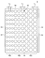
- FIG. 2 is a diagram illustrating a light reflecting surface of the light guide plate.
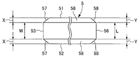
- FIG. 3 is a perspective view of the light guide plate.
- FIG. 4 is a diagram for explaining chamfering formed on the light guide plate.
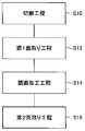
- Drawing 5 is a flowchart of a manufacturing method of a glass member which is a certain embodiment.
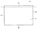
- Drawing 6 is a figure for explaining the cutting composition of the manufacturing method of the glass member which is a certain embodiment.
- FIG. 7 is a diagram for explaining the mirror surface processing step.
- FIGS. 8A to 8B are diagrams for explaining the relationship between the surface roughness Ra of the samples according to Examples 1 to 6 and the transmittance difference.
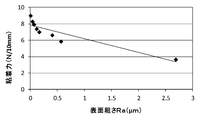
- FIG. 9 is a diagram for explaining the relationship between the surface roughness Ra and the adhesive force P of the samples according to Examples 7 to 14.
- FIG. 10 is a diagram for explaining the relationship between the surface rough
- FIG. 1 shows a liquid crystal display device 1 using a glass member according to an embodiment of the present invention.
- the liquid crystal display device 1 is mounted on an electronic device that is reduced in size and thickness, such as a portable information terminal.
- the liquid crystal display device 1 has a liquid crystal panel 2 and a planar light emitting device 3.
- the liquid crystal panel 2 includes an alignment layer, a transparent electrode, a glass substrate, and a polarizing filter so as to sandwich a liquid crystal layer disposed in the center.
- a color filter is disposed on one side of the liquid crystal layer.
- the molecules of the liquid crystal layer rotate around the light distribution axis by applying a driving voltage to the transparent electrode, thereby performing a predetermined display.
- the planar light emitting device 3 adopts an edge light type in order to reduce the size and thickness.
- the planar light emitting device 3 includes a light source 4, a light guide plate 5, a reflection sheet 6, a diffusion sheet 7, and reflection dots 10A to 10C.
- the light incident on the light guide plate 5 from the light source 4 travels while being reflected by the reflection dots 10A to 10C and the reflection sheet 6, and is emitted from the light emission surface 51 of the light guide plate 5 facing the liquid crystal panel 2.
- the light emitted from the light emitting surface 51 is diffused by the diffusion sheet 7 and then enters the liquid crystal panel 2.
- the light source 4 is not particularly limited, and a hot cathode tube, a cold cathode tube, or an LED (Light Emitting Diode) can be used.
- the light source 4 is disposed to face the light incident end surface 53 of the light guide plate 5.
- a reflector 8 is provided on the back side of the light source 4 in order to increase the incident efficiency of the light emitted radially from the light source 4 to the light guide plate 5.
- the reflection sheet 6 is configured such that a light reflection member is coated on the surface of a resin sheet such as an acrylic resin.
- the reflection sheet 6 is disposed on the light reflection surface 52 and the non-light-incident end surfaces 54 to 56 of the light guide plate 5.
- the light reflecting surface 52 is a surface facing the light emitting surface 51 of the light guide plate 5.
- the non-light-incident end surfaces 54 to 56 are surfaces other than the light incident end surface 53 at the end surfaces of the light guide plate 5.
- the glass member has a light guide plate 5 and a reflection sheet 6, and the reflection sheet 6 is disposed at least on the non-light-incident end face 56 facing the light-incident end face 53.
- the reflection sheet 6 can reflect the light again into the light guide plate 5.
- the reflection sheet 6 is more preferably disposed also on the non-light-incident end surfaces 54 and 55.
- the material of the resin sheet constituting the reflection sheet 6 is not limited to an acrylic resin, and for example, a polyester resin such as a PET resin, a urethane resin, and a material formed by combining them can be used.
- the light reflecting member constituting the reflecting sheet 6 for example, a metal vapor deposition film or the like can be used.
- the reflective sheet 6 disposed on the non-light-incident end surfaces 54 to 56 is provided with an adhesive.
- an adhesive provided in the reflection sheet 6 for example, an acrylic resin, a silicone resin, a urethane resin, a synthetic rubber, or the like can be used.
- the reflection sheet 6 is disposed on the non-light-incident end surfaces 54 to 56 via an adhesive.
- the thickness of the reflection sheet 6 is not particularly limited, but for example, a thickness of 0.01 to 0.50 mm can be used.
- the diffusion sheet 7 can be a milky white acrylic resin film or the like. Since the diffusion sheet 7 diffuses the light emitted from the light emitting surface 51 of the light guide plate 5, the back side of the liquid crystal panel 2 can be irradiated with uniform light without uneven brightness.
- the reflection sheet 6 and the diffusion sheet 7 are fixed to predetermined positions of the light guide plate 5 by, for example, adhesion.
- the light guide plate 5 is made of highly transparent glass.
- multi-component oxide glass is used as the glass material used for the light guide plate 5.
- the light guide plate 5 is made of glass having an effective optical path length of 5 to 200 cm and an average internal transmittance of 80% or more in the visible light region (wavelength 380 nm to 800 nm) at the effective optical path length. .
- the average internal transmittance in the visible light region of the glass is preferably 82% or more, more preferably 85% or more, and still more preferably 90% or more in terms of effective optical path length.
- the effective optical path length of glass refers to the distance from the light incident end surface where light enters when the light guide plate is used, to the opposite non-light incident end surface. In the case of the light guide plate 5 shown in FIG. Corresponds to the length of the direction.
- the average internal transmittance T ave in the visible light region of the glass can be calculated by an evaluation method described later.
- the Y value of the tristimulus value in the XYZ color system in JIS Z8701 (Appendix) of the glass used as the light guide plate 5 in an effective optical path length is 90% or more.
- S ( ⁇ ) is a transmittance at each wavelength
- y ( ⁇ ) is a weighting coefficient for each wavelength. Therefore, ⁇ (S ( ⁇ ) ⁇ y ( ⁇ )) is the sum of the product of the weighting coefficient of each wavelength and its transmittance.
- y ( ⁇ ) corresponds to the M cone (G cone / green) among the retinal cells of the eye, and is most responsive to light having a wavelength of 535 nm.
- the Y value is more preferably 91% or more, more preferably 92% or more, and particularly preferably 93% or more in terms of effective optical path length.
- a method for evaluating the internal transmittance T in and the average internal transmittance T ave in the visible light region of glass will be described. First, a sample A having a size of 50 mm in length and 50 mm in width is collected by cleaving from a substantially central portion of a target glass plate in a direction perpendicular to the first main surface of the glass plate. Next, it is confirmed that the arithmetic average roughness Ra of the first and second fractured surfaces facing each other of the sample A is 0.03 ⁇ m or less.
- the first and second fractured surfaces are polished with free abrasive grains of colloidal silica or cerium oxide.
- the first fractured face, the normal direction of the first split section, at 50mm length measuring the transmittance T A in the wavelength range of 400 nm ⁇ 800 nm.
- 50 mm spectrometer capable of measuring in length e.g., UH4150: Hitachi High-Technologies Corporation
- the slit or the like smaller than the thickness of the beam width of the incident light And measure.
- ⁇ is a wavelength.
- T in [ ⁇ (1-R A ) 2 + ⁇ (1-R A ) 4 + 4T A 2 R A 2 ⁇ 0.5 ] / (2T A R A 2 ) (3)
- the average internal transmittance of the glass plate T ave is calculated.
- the total amount A of iron in the glass used as the light guide plate 5 is preferably 150 ppm or less in order to satisfy the above-described average internal transmittance and Y value in the visible light region with the effective optical path length, and 80 ppm or less. More preferably, it is more preferably 50 ppm or less.
- the total amount A of the iron content of the glass used as the light guide plate 5 is preferably 5 ppm or more in order to improve the meltability of the glass during the production of multi-component oxide glass. More preferably, it is more preferably 20 ppm or more.
- the total amount A of the iron content of the glass used as the light guide plate 5 can be adjusted by the amount of iron added at the time of glass production.
- the total iron content A of the glass is expressed as the content of Fe 2 O 3 , but all the iron present in the glass exists as Fe 3+ (trivalent iron). I don't mean.
- Fe 3+ and Fe 2+ are simultaneously present in the glass.
- Fe 2+ and Fe 3+ which is absorbed in the visible light region is present, an order of magnitude than the absorption coefficient of the absorption coefficient of the Fe 2+ (11cm -1 Mol -1) is Fe 3+ (0.96cm -1 Mol -1) Since it is large, the internal transmittance in the visible light region is further reduced. Therefore, it is preferable that the Fe 2+ content is small in order to increase the internal transmittance in the visible light region.
- the glass used as the light guide plate 5 can suppress the absorption of light at a wavelength of 600 nm to 780 nm when the content of Fe 2+ of the glass satisfies the conditions described later, and depends on the size of the display such as an edge light type. Even when the effective optical path length changes, it can be used effectively.
- the glass used as the light guide plate 5 is 2.5 (cm ⁇ ppm) when the effective optical path length is L (cm) and the Fe 2+ content is B (ppm, converted to Fe 2 O 3 ). ⁇ L ⁇ B ⁇ 3000 (cm ⁇ ppm) is preferably satisfied. If L ⁇ B ⁇ 2.5 (cm ⁇ ppm), the content of Fe 2+ of glass used as a light guide plate 5 to be used in planar light emitting device of a size effective optical path length is 25 ⁇ 200 cm B 0 .05-0.1 ppm, making mass production at low cost difficult.
- the content of Fe 2+ in the glass used as the light guide plate 5 increases, so that the absorption of light at a wavelength of 600 nm to 780 nm increases, and the internal transmittance in the visible light range. May decrease, and the average internal transmittance and Y value of the visible light region described above may not be satisfied with the effective optical path length.
- the glass used as the light guide plate 5 more preferably satisfies the relationship of 10 (cm ⁇ ppm) ⁇ L ⁇ B ⁇ 2400 (cm ⁇ ppm), and 25 (cm ⁇ ppm) ⁇ L ⁇ B ⁇ 1850 ( More preferably, the relationship cm ⁇ ppm) is satisfied.
- the Fe 2+ content B of the glass used as the light guide plate 5 is preferably 30 ppm or less in order to satisfy the above-described average internal transmittance and Y value in the visible light region with the effective optical path length, and is 20 ppm or less. More preferred is 10 ppm or less.
- the Fe 2+ content B of the glass used as the light guide plate 5 is preferably 0.02 ppm or more from the viewpoint of improving the meltability of the glass during the production of multi-component oxide glass. It is more preferably 0.05 ppm or more, and further preferably 0.1 ppm or more.
- content of Fe ⁇ 2+> of the glass used as the light-guide plate 5 can be adjusted with the quantity of the oxidizing agent added at the time of glass manufacture. Specific types of oxidizers added during glass production and their addition amounts will be described later.
- the content A of Fe 2 O 3 is determined by the fluorescent X-ray measurement, a content of total iron as calculated as Fe 2 O 3 (mass ppm).
- the Fe 2+ content B is measured according to ASTM C169-92. The measured Fe 2+ content is expressed in terms of Fe 2 O 3 .
- the multi-component oxide glass used as the light guide plate 5 has a low content of components having absorption in the visible light region, and the average internal transmittance and Y value in the visible light region described above in terms of the effective optical path length. It is preferable in satisfying.
- components having absorption in the visible light region include MnO 2 , TiO 2 , NiO, CoO, V 2 O 5 , CuO, and Cr 2 O 3 .
- the glass used as the light guide plate 5 has a total content of these components (at least one selected from the group consisting of MnO 2 , TiO 2 , NiO, CoO, V 2 O 5 , CuO and Cr 2 O 3 ) oxidized.
- It is preferably 0.1% or less (1000 ppm or less) in terms of mass percentage on an object basis in order to satisfy the above-described average internal transmittance and Y value in the visible light region with the effective optical path length. More preferably, it is 0.08% or less (800 ppm or less), More preferably, it is 0.05% or less (500 ppm or less).
- composition of the glass used as the light guide plate 5 are shown below. However, the composition of the glass used as the light guide plate 5 is not limited to these.
- the composition of the glass excluding iron is expressed in terms of mass percentage on an oxide basis, SiO 2 : 60 to 80%, Al 2 O 3 : 0 to 7%, MgO: 0 to 10%, CaO: 4 to 20%, Na 2 O: 7 to 20%, K 2 O: 0 to 10%.
- composition of the glass excluding iron is expressed in terms of mass percentage on the basis of oxide, SiO 2 : 45 to 80%, Al 2 O 3 : More than 7% and 30% or less, B 2 O 3 : 0 to 15%, MgO: 0 to 15%, CaO: 0 to 6%, Na 2 O: 7 to 20%, K 2 O: 0 to 10% , ZrO 2 : 0 to 10%.
- Still another structural example (Structural Example C) of the glass used as the light guide plate 5 is that the composition of the glass excluding iron is expressed in terms of mass percentage on the basis of oxide, SiO 2 : 45 to 70%, Al 2 O 3 : 10 to 30%, B 2 O 3 : 0 to 15%, at least one selected from the group consisting of MgO, CaO, SrO and BaO: 5 to 30%, Li 2 O, Na 2 O and K 2 At least one selected from the group consisting of O: 0% or more and less than 7%.
- the glass used as the light guide plate 5 is not limited to these.
- the light guide plate 5 includes a light emitting surface 51 (first surface), a light reflecting surface 52 (second surface), and a light incident end surface 53 (first end surface). , Non-light-incident end surfaces 54 to 56 (second end surface), light-incident side chamfered surfaces 57 (first chamfered surfaces), and non-light-incident side chamfered surfaces 58 (second chamfered surfaces).
- the light emitting surface 51 is a surface facing the liquid crystal panel 2.
- the light emitting surface 51 has a rectangular shape in a plan view (a state in which the light emitting surface 51 is viewed from above).
- the shape of the light emission surface 51 is not limited to this.
- the size of the light emitting surface 51 is not particularly limited because it is determined corresponding to the liquid crystal panel 2.
- the size of the light emitting surface 51 is, for example, 1200 mm ⁇ 700 mm.
- the light reflecting surface 52 is a surface facing the light emitting surface 51.
- the light reflecting surface 52 is configured to be parallel to the light emitting surface 51.
- the shape and size of the light reflecting surface 52 are configured to be the same as those of the light emitting surface 51.
- the light reflecting surface 52 does not necessarily have to be parallel to the light emitting surface 51, and may have a stepped or inclined structure. Further, the size of the light reflecting surface 52 may be different from that of the light emitting surface 51.
- reflective dots 10A to 10C are formed on the light reflecting surface 52.
- the reflective dots 10A to 10C are obtained by printing white ink in dots.
- the luminance of the light incident from the light incident end surface 53 is strong, and the luminance is lowered by reflecting and proceeding in the light guide plate 5.
- the size of the reflective dots 10A to 10C is varied from the light incident end face 53 toward the light traveling direction (to the right in FIGS. 1 and 2). Specifically, the diameter (L A ) of the reflective dot 10A in the region close to the light incident end face 53 is set to be small, and the diameter (L B ) of the reflective dot 10B and the reflective dot are gradually increased in the light traveling direction. radius of 10C diameter (L C) are set so that the larger (L a ⁇ L B ⁇ L C).
- each reflective dot 10A by changing the size of each reflective dot 10A toward the traveling direction of the light in the light guide plate 5, the brightness of the emitted light emitted from the light emitting surface 51 can be made uniform, and uneven brightness is generated. Can be suppressed.
- the same effect can also be obtained by changing the number density of each reflective dot 10A in the light traveling direction in the light guide plate 5 instead of the size of each reflective dot 10A. Further, the same effect can be obtained by forming a groove on the light reflecting surface 52 to reflect the incident light instead of the reflecting dot 10A.
- the light incident end surface 53 that is the first end surface is a surface on which light is incident from the light source 4 described above.
- the non-light incident end surfaces 54 to 56 that are the second end surfaces are surfaces on which light is not incident from the light source 4.
- the surface roughness Ra of the non-light-incident end surfaces 54 to 56 is set to 0.8 ⁇ m or less.
- the reason why the surface roughness Ra of the non-light-incident end faces 54 to 56 is set to 0.8 ⁇ m or less is as follows. In the following description, when the surface roughness Ra is described, it means the arithmetic average roughness (centerline average roughness) according to JIS B 0601 to JIS B 0031.
- the reflection sheet 6 is adhered to the non-light-incident end surfaces 54 to 56.
- the surface roughness Ra of the non-light-incident end surfaces 54 to 56 is in a rough state exceeding 0.8 ⁇ m, the reflection sheet 6 cannot properly adhere to the non-light-incident end surfaces 54 to 56.
- the surface roughness Ra of the non-light-incident end surfaces 54 to 56 is 0.8 ⁇ m or less, the adhesiveness of the reflective sheet 6 to the non-light-incident end surfaces 54 to 56 becomes good.
- the peeling of the reflective sheet 6 is prevented, and the reliability of the planar light emitting device 3 can be increased.
- the surface roughness Ra of the non-light-incident end faces 54 to 56 is preferably 0.4 ⁇ m or less, more preferably 0.2 ⁇ m or less, further preferably 0.1 ⁇ m or less, and particularly preferably 0.04 ⁇ m or less. is there.
- the non-light-incident end surfaces 54 to 56 are not subjected to grinding or polishing. Therefore, the surface roughness Ra of the non-light-incident end surfaces 54 to 56 is set to be larger than the surface roughness Ra of the light-incident end surface 53, and preferably the surface roughness Ra of the non-light-incident end surfaces 54 to 56. Is 0.01 ⁇ m or more, more preferably 0.03 ⁇ m or more. As a result, the processing of the non-light-incident end surfaces 54 to 56 is easier or unnecessary than the light-incident end surface 53, and the productivity is improved.
- the non-light-incident end surfaces 54 to 56 may be ground or polished, and the surface roughness Ra of the non-light-incident end surfaces 54 to 56 is equal to the surface roughness Ra of the light-incident end surface 53. May be. That is, the surface roughness Ra of the non-light-incident end surfaces 54 to 56 is preferably equal to or greater than the surface roughness Ra of the light-incident end surface 53, and the surface roughness Ra of the non-light-incident end surfaces 54 to 56 is the surface of the light-incident end surface 53. More preferably, it is larger than the roughness Ra.
- the width dimension of the non-light-incident end surfaces 54 to 56 (that is, of the surfaces provided between the first surface and the second surface, excluding the non-light-incident side chamfering surface 58 described later).
- the dimension of the portion in the plate thickness direction is L (mm)
- the average value L ave in the longitudinal direction of the chamfered surface (hereinafter simply referred to as the longitudinal direction) of the width dimension L is 0.25 to 9.8 mm. Is preferred.
- L ave is more preferably 0.50 to 9.8 mm. If L ave is 9.8 mm or less, the width dimension Y of the non-light-incident side chamfer 58 can be sufficiently secured. If L ave is 0.25 mm or more, an error of L described later can be reduced.
- the error relative to L ave in the longitudinal direction of L is preferably within 50% of L ave . That is, when the maximum value in the longitudinal direction of L is L max (mm) and the minimum value is L min (mm), L max ⁇ 1.5 ⁇ L ave and L min ⁇ 0.5 ⁇ L ave are satisfied. preferable.
- the error is more preferably within 40%, still more preferably within 30%, and particularly preferably within 20%.
- the reflection sheet 6 is disposed on the non-light-incident end surfaces 54 to 56 as described above, but a gap due to adhesion failure occurs at the interface between the non-light-incident end surfaces 54 to 56 and the reflective sheet 6.
- the ratio of the area occupied by the gap per unit area at the interface between the non-light-incident end face and the reflective sheet (hereinafter also simply referred to as area void ratio) is the surface roughness Ra and shape of the non-light-incident end faces 54 to 56, the reflective sheet 6 can be made small by appropriately selecting the pressure-sensitive adhesive contained in 6.
- the area porosity at the interface between the non-light-incident end surfaces 54 to 56 and the reflection sheet 6 is preferably 40% or less, more preferably 30% or less, and further preferably 20% or less.
- the area porosity is 40% or less, it is possible to suppress a decrease in luminance that occurs due to the gap when light is reflected on the reflection sheet 6 by the light guide plate 5.
- the area porosity can be calculated by the following method. First, the peel strength P (N / 10 mm) of the reflective sheet with respect to the non-light-incident end face at the interface between the non-light-incident end face and the reflective sheet to be calculated is measured.
- the peeling adhesive strength P (N / 10 mm) can be measured by a peeling adhesive strength test defined in JIS Z 0237. Thereafter, non have light incident face the same glass composition and shape, the surface against the end face of the roughness glass Ra of less 0.0050Myuemu, peel adhesion of the reflective sheet against the end face P 0 (N / 10 mm) is measured in the same manner.
- the area porosity of the end face having a surface roughness Ra of 0.0050 ⁇ m or less is 0%
- the light incident end face 53 is preferably mirror-finished when the glass that is the light guide plate 5 is manufactured. Specifically, it is preferable that the arithmetic average roughness (centerline average roughness) Ra of the surface of the light incident end face 53 is 0.03 ⁇ m or less. Thereby, the light incident efficiency of the light which enters into the light-guide plate 5 from the light source 4 is improved.
- the width dimension W (see FIG. 4) of the light incident end face 53 is set to a width dimension required from the liquid crystal display device 1 on which the planar light emitting device 3 is mounted.
- the surface roughness Ra of the light incident end face 53 is preferably 0.01 ⁇ m or less, and more preferably 0.005 ⁇ m or less.
- a light incident side surface 57 is formed between the light emitting surface 51 and the light incident end surface 53 and between the light reflecting surface 52 and the light incident end surface 53.
- the thickness t of the light guide plate 5 according to the present embodiment is 10 mm or less.
- the light guide plate 5 according to the present embodiment preferably has a thickness t of 0.5 mm or more, and a light incident side chamfer 57 is formed on the upper and lower edges of the light incident end surface 53. .
- the area of the light incident end face 53 needs to be increased. For this reason, it is desirable that the light incident side chamfered surface 57 be small. For this reason, in this embodiment, the light incident side chamfered surface 57 is chamfered.
- the width dimension of the light incident side chamfered surface 57 is X (mm)
- the average of the width dimension X in the longitudinal direction of the chamfered surface (hereinafter simply referred to as the longitudinal direction).
- the value X ave is preferably from 0.01 mm to 0.5 mm, more preferably from 0.05 mm to 0.5 mm, and particularly preferably from 0.1 mm to 0.5 mm. If X ave is 0.5 mm or less, the width dimension W of the light incident end face 53 can be increased. If X ave is 0.1 mm or more, the error of X described later can be reduced. When X ave is 0.01 mm or more, breakage starting from a chamfered surface can be suppressed, and handling properties can be improved.
- the error in the longitudinal direction of X is preferably within 50% of X ave . That is, X preferably satisfies 0.5X ave ⁇ X ⁇ 1.5X ave .
- the error is more preferably within 40%, still more preferably within 30%, and particularly preferably within 20%.
- the surface roughness Ra of the light incident side chamfer 57 is preferably 0.4 ⁇ m or less.
- the surface roughness Ra of the light incident side chamfering surface 57 is more preferably 0.3 ⁇ m or less, and further preferably 0.1 ⁇ m. Or less, particularly preferably 0.03 ⁇ m or less.
- the width dimension of the non-light-incident side chamfer 58 is Y (mm)
- the average value Y ave in the longitudinal direction of the width dimension Y is 0.1 to 0.6 (mm). ) Is preferable. If Y ave is 0.6 mm or less, the width L of the non-light-incident end surfaces 54 to 56 can be increased. If Y ave is 0.1 mm or more, the error of Y described later can be reduced.
- the error in the longitudinal direction of Y is preferably within 50% of Y ave . That is, Y preferably satisfies 0.5Y ave ⁇ Y ⁇ 1.5Y ave .
- the error is more preferably within 40%, still more preferably within 30%, and particularly preferably within 20%.
- the surface roughness Ra of the non-light-incident side chamfered surface 58 is larger than the surface roughness Ra of the light-incident side chamfered surface 57 from the viewpoint of improving productivity, preferably 0.03 ⁇ m or more, more preferably 0.1 ⁇ m or more. More preferably, it is 0.3 ⁇ m or more, and particularly preferably 0.4 ⁇ m or more. Further, the surface roughness Ra of the non-light-incident side chamfered surface 58 is preferably 1.0 ⁇ m or less.
- the surface roughness Ra of the non-light-incident side chamfering surface 58 is 0.4 ⁇ m or more and 1.0 ⁇ m or less, when the reflective sheet 6 is adhered to the non-light-incident side chamfering surface 58, the adhesiveness between the two is reduced. Becomes better. In addition, luminance unevenness generated in the light guide plate 5 can be reduced.
- FIG. 5 to 7 are diagrams for explaining a method of manufacturing the light guide plate 5.
- FIG. 5 is a process diagram showing a method for manufacturing the light guide plate 5.
- a glass material 12 is prepared. As described above, this glass material has an effective optical path length of 5 to 200 cm, a thickness of preferably 0.5 to 10 mm, and an average internal transmittance in the visible light region with an effective optical path length of 80% or more.
- the Y value of the tristimulus value in the XYZ color system in JIS Z8701 (Appendix) is preferably 90% or more.
- the glass material 12 has a shape larger than the predetermined shape of the light guide plate 5.
- the glass material 12 is first subjected to a cutting process shown in step 10 in FIG. 5 (step is abbreviated as S in the figure).
- a cutting process is performed at each position (one incident light end face side position and three non-light incident end face side positions) indicated by broken lines in FIG. 6 using a cutting device. Note that the cutting process does not necessarily have to be performed on the three non-light-incident end face side positions, and only one non-light-incident end face side position facing the one light incident end face-side position is cut. May be.
- the glass substrate 14 is cut from the glass material 12 by performing a cutting process.
- the light guide plate 5 since the light guide plate 5 has a rectangular shape in plan view, cutting processing is performed on one light incident end surface side position and three non-light incident end surface side positions. However, the cutting position is appropriately selected according to the shape of the light guide plate 5.
- the first chamfering step (step 12) is performed.
- a non-light-incident side chamfer 58 is provided between the light-emitting surface 51 and the non-light-incident end surface 56 and between the light-reflecting surface 52 and the non-light-incident end surface 56 using a grinding device.
- chamfering may be performed between the light emitting surface 51 and the light incident end surface 53 or between the light reflecting surface 52 and the light incident end surface 53.
- the surface roughness Ra of the chamfered surface obtained is larger than the surface roughness Ra of the light incident side chamfered surface 57 obtained in the second chamfering step described later.
- the non-light-incident end surfaces 54 to 56 are ground or polished in the first chamfering step.
- the grinding process or the polishing process for the non-light-incident end surfaces 54 to 56 may be performed before or after the above-described non-light-incident side chamfering surface 58 is formed, or may be performed simultaneously.
- the first chamfering step (step 12) can be performed at the same time as or after the mirror chamfering step (step 14) and the second chamfering step (step 16), which will be described later, but is preferably performed before them.
- the processing according to the shape of the light guide plate 5 can be performed at a relatively fast rate in step 12, so that productivity is improved and a relatively large cullet generated in step 12
- the light chamfered surface 57 is hardly damaged.
- the mirror finishing process is then performed (step 14).
- the light incident end surface 53 is formed by performing mirror surface processing on the light incident end surface side of the glass substrate 14.
- the light incident end surface 53 is a surface on which light is incident from the light source 4. Therefore, the light incident end face 53 is mirror-finished so that the surface roughness Ra is 0.03 ⁇ m or less.
- step 16 When the light incident end face 53 is formed on the glass base material 14 in the mirror finishing process (step 14), the second chamfering process (step 16) is subsequently performed, so that the light emitting face 51 and the light incident end face 53 are separated.
- a light incident side chamfered surface 57 (chamfered surface) is formed by grinding or polishing between the light reflecting surface 52 and the light incident end surface 53. Note that step 16 can be performed before step 14 or can be performed simultaneously with step 14.
- a grindstone When forming the light incident side chamfered surface 57, a grindstone may be used as a tool for performing grinding treatment or polishing treatment. In addition to a grindstone, a buff or brush made of cloth, leather, rubber or the like is used. Also good. At that time, an abrasive such as cerium oxide, alumina, carborundum, colloidal silica or the like may be used.
- the light guide plate 5 is manufactured by carrying out the steps shown in steps 10 to 16 above.
- the reflective dots 10A to 10C are printed on the light reflecting surface 52 after the light guide plate 5 is manufactured.
- the 2 O 13.9%, 0.05% and K 2 O was used a glass plate comprising Fe 2 O 3 0.005% (vertical 50 mm, lateral 50 mm, thickness 2.5 mm).
- the glass plate was cut out from a glass plate produced by the float process in a cutting process (when the glass was cut, the corner portion of the glass was cut to prevent breakage).
- the glass has four end surfaces between the light emitting surface and the light reflecting surface, and among the four end surfaces, one end surface is a light incident end surface and three end surfaces are non-light incident end surfaces. .
- the first chamfering process was performed after the cutting process.
- the three non-light-incident end surfaces were ground. Furthermore, using a grinding device, between the light emitting surface and the non-light-receiving end surface of the glass, between the light reflecting surface and the non-light-receiving end surface, between the light emitting surface and the light-receiving end surface, or light reflection Chamfering was performed between the surface and the light incident end surface.
- Example 1 First, an experiment was conducted to examine the relationship between Ra on the non-light-incident end face and light transmittance.
- Table 1 shows the surface roughness Ra of the non-light-incident end surfaces of the samples according to Examples 1 to 6, respectively.
- a mirror finishing process was performed.
- mirror surface processing was performed on the light incident end surface.
- the surface roughness Ra of the light incident end face of each of the obtained samples according to Examples 1 to 6 was 0.01 ⁇ m.
- a second chamfering process is performed following the mirror finishing process, and a grinding process is performed between the light emitting surface and the light incident end surface and between the light reflecting surface and the light incident end surface to form a light incident side chamfered surface. did.
- the transmittance of the non-light-incident end face was measured for the samples according to Examples 1 to 6.
- light having a wavelength of 400 nm to 800 nm was incident from the light incident end face side toward the non-light incident end face opposed to the light incident end face, and the average transmittance was calculated from the measured values of the transmittance.
- the same measurement was performed on a reference sample in which the non-light-incident end face was optically polished, and the average transmittance at wavelengths of 400 nm to 800 nm was calculated.
- Table 1 shows the difference values (hereinafter also simply referred to as transmittance differences) obtained by subtracting the average transmittance of the reference samples at wavelengths of 400 nm to 800 nm from the average transmittance of the samples according to Examples 1 to 6 at wavelengths of 400 nm to 800 nm. It shows together with.
- FIGS. 8 (a) to 8 (b) Both FIG. 8A and FIG. 8B are obtained by plotting the surface roughness Ra and the transmittance difference shown in Table 1, and only the range showing the approximate straight line is changed.
- the transmittance difference cannot be ignored.
- the transmittance difference is less than ⁇ 50%, so that most of the incident light that does not pass through the non-light-incident end face is diffusely reflected (diffuse reflection) at the non-light-incident end face. This causes a decrease in luminance.
- Example 2 Next, an experiment was conducted to examine the relationship between the adhesive area between the non-light-incident end face and the reflective sheet and the adhesive force.
- a reflective sheet manufactured by Teraoka Seisakusho, product name: light-shielding polyester film adhesive tape, product number: No. 6370
- the surface roughness Ra is 0.0044 ⁇ m.
- Each was placed on a glass surface.
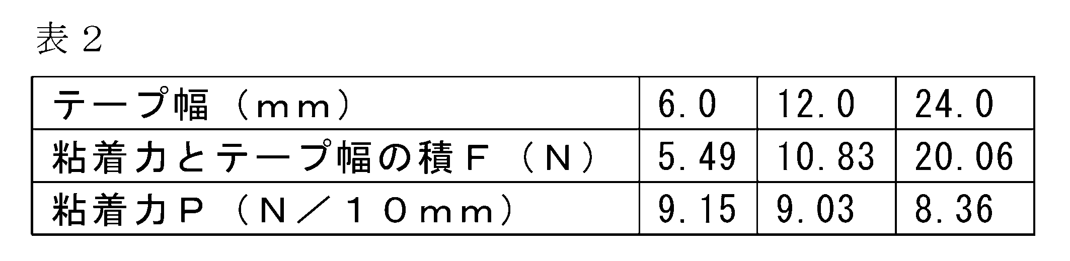
- a testing machine As a testing machine, a desktop precision universal testing machine (manufactured by Shimadzu Corporation, model name: AGS-5kNX) was used. The peel adhesion test was performed five times for each sample, and the average value of adhesive strength P (N / 10 mm) (hereinafter referred to as the product F (N) of the measured adhesive strength and tape width) , Also simply referred to as adhesive strength). These are shown in Table 2.
- the adhesive area and the area void ratio are relatively calculated by performing a peel adhesion test using a reflective sheet having the same material and the same area on a sample having a plurality of surface roughness Ra. Can do.
- the adhesive tape / adhesive sheet peeling adhesive strength test defined in JIS Z 0237 was conducted in the same manner as in Experiment 2, and the peeling adhesive strength test was conducted 5 times for each sample.
- the average value of the measured adhesive strength P (N / 10 mm) (hereinafter also simply referred to as adhesive strength) was calculated.
- Table 3 shows the adhesive strength P at the interface between the non-light-incident end face and the reflective sheet of the samples according to Examples 7 to 22, respectively.
- Table 3 also shows the area porosity calculated from the adhesive force P when the area porosity in Example 7 and Example 15 is 0%.
- FIG. 9 shows the relationship between the surface roughness Ra of the samples according to Examples 7 to 14 and the adhesive strength P
- FIG. 10 shows the relationship between the surface roughness Ra of the samples according to Examples 15 to 22 and the adhesive strength P. Respectively.
Landscapes
- Physics & Mathematics (AREA)
- General Physics & Mathematics (AREA)
- Optics & Photonics (AREA)
- Chemical & Material Sciences (AREA)
- Engineering & Computer Science (AREA)
- Chemical Kinetics & Catalysis (AREA)
- Life Sciences & Earth Sciences (AREA)
- General Chemical & Material Sciences (AREA)
- Geochemistry & Mineralogy (AREA)
- Materials Engineering (AREA)
- Organic Chemistry (AREA)
- General Engineering & Computer Science (AREA)
- Planar Illumination Modules (AREA)
- Surface Treatment Of Glass (AREA)
- Liquid Crystal (AREA)
Abstract
Description
ガラスと反射シートを有するガラス部材であって、
前記ガラスは、第1面と、
前記第1面に対向する第2面と、
前記第1面と前記第2面の間に設けられる少なくとも1つの第1端面と、
前記第1面と前記第2面の間に設けられ前記第1端面とは異なる少なくとも1つの第2端面を有し、
前記ガラスの有効光路長が5~200cmであり、
前記ガラスの有効光路長での可視光域の平均内部透過率が80%以上であり、
前記第2端面の表面粗さRaが0.8μm以下であり、
前記第2端面には前記反射シートが配設される、ガラス部材を提供する。
第1面と、
前記第1面に対向する第2面と、
前記第1面と前記第2面の間に設けられる少なくとも1つの第1端面と、
前記第1面と前記第2面の間に設けられ前記第1端面とは異なる少なくとも1つの第2端面を有するガラスであって、
前記ガラスの有効光路長が5~200cmであり、
前記ガラスの有効光路長での可視光域の平均内部透過率が80%以上であり、
前記第2端面の表面粗さRaが0.8μm以下であるガラス部材をも提供する。
また、導光板5として用いられるガラスの、有効光路長でのJIS Z8701(附属書)でのXYZ表色系における三刺激値のY値が90%以上であることが好ましい。Y値は、Y=Σ(S(λ)×y(λ))により求められる。ここで、S(λ)は、各波長における透過率であり、y(λ)は各波長の重みづけ係数である。従って、Σ(S(λ)×y(λ))は、各波長の重みづけ係数と、その透過率と、を掛け合わせたものの総和を取ったものである。なお、y(λ)は、眼の網膜細胞のうち、M錐体(G錐体/緑)に対応し、波長535nmの光に最も反応する。Y値は、有効光路長で91%以上がより好ましく、92%以上がさらに好ましく、93%以上が特に好ましい。
ガラスの可視光域の内部透過率Tinおよび平均内部透過率Taveの評価方法について説明する。
まず、対象となるガラス板の略中央部分から、ガラス板の第1の主表面に垂直な方向で割断することにより、縦50mm×横50mmの寸法のサンプルAを採取する。次に、このサンプルAの相互に対向する第1および第2の割断面の算術平均粗さRaが、0.03μm以下となっていることを確認する。もし、算術平均粗さRaが0.03μmより大きい場合、第1および第2の割断面をコロイダルシリカまたは酸化セリウムの遊離砥粒で研磨する。次に、このサンプルAにおいて、第1の割断面に対して、該第1の割断面の法線方向で、50mm長での、波長400nm~800nmの範囲における透過率TAを測定する。透過率TAの測定においては、50mm長での測定が可能な分光測定装置(たとえば、UH4150:日立ハイテクノロジーズ社製)を使用し、スリット等によって、入射光のビーム幅を板厚よりも狭くして測定する。
nA=[1+{B1λ2/(λ2-C1)}+{B2λ2/(λ2-C2)}+{B3λ2/(λ2-C3)}]0.5 (1)
なお、式(1)において、λは波長である。
RA=(1-nA)2/(1+nA)2 (2)
Tin=[-(1-RA)2+{(1-RA)4+4TA 2RA 2}0.5]/(2TARA 2) (3)
V=100×(1-P/P0) (式1)
まず、非入光端面のRaと光の透過率の関係を調べるための実験を行った。
例1~6に係るサンプルの非入光端面の表面粗さRaをそれぞれ表1に示す。

次に、非入光端面と反射シートとの粘着面積と、粘着力との関係を調べるための実験を行った。まず、テープ幅がそれぞれ6mm、12mm、24mmである反射シート(寺岡製作所社製、製品名:遮光用ポリエステルフィルム粘着テープ、品番:No.6370)を用意し、表面粗さRaが0.0044μmであるガラス表面の上にそれぞれ配設した。これらのサンプルに対し、JIS Z 0237に定められる粘着テープ・粘着シートの180°引きはがし粘着力試験を行った。試験機としては、卓上型精密万能試験機(島津製作所社製、型名:AGS-5kNX)を使用した。該引きはがし粘着力試験を、1つのサンプルに対して5回ずつ行い、測定された粘着力とテープ幅の積F(N)の値から、粘着力P(N/10mm)の平均値(以下、単に粘着力ともいう)を算出した。これらを表2に示す。
続いて、非入光端面の表面粗さRaが該非入光端面と反射シートとの粘着力に与える影響を調べるための実験を行った。まず、テープ幅が12mmである反射シート(寺岡製作所社製、製品名:遮光用ポリエステルフィルム粘着テープ、品番:No.6370)を用意し、表面粗さRaがそれぞれ0.0044μm、0.0395μm、0.0677μm、0.1170μm、0.1640μm、0.4040μm、0.5670μm、2.686μmであるガラス表面の上にそれぞれ配設した。これらのサンプルをそれぞれ例7~14とする。また、テープ幅が24mmである反射シートについても同様に、表面粗さRaがそれぞれ0.0044μm、0.0395μm、0.0677μm、0.117μm、0.164μm、0.404μm、0.567μm、2.686μmであるガラス表面の上にそれぞれ配設した。これらのサンプルをそれぞれ例15~22とする。

なお、本出願は、2015年2月12日付けで出願された日本特許出願(特願2015-025339)に基づいており、その全体が引用により援用される。
2 液晶パネル
3 面状発光装置
4 光源
5 導光板(ガラス)
6 反射シート
7 拡散シート
8 リフレクタ
10A~10C 反射ドット
12 ガラス素材
14 ガラス基材
51 光出射面(第1面)
52 光反射面(第2面)
53 入光端面(第1端面)
54,55,56 非入光端面(第2端面)
57 入光側面取り面(第1面取り面)
58 非入光側面取り面(第2面取り面)
Claims (12)
- ガラスと反射シートを有するガラス部材であって、
前記ガラスは、第1面と、
前記第1面に対向する第2面と、
前記第1面と前記第2面の間に設けられる少なくとも1つの第1端面と、
前記第1面と前記第2面の間に設けられ、前記第1端面とは異なる少なくとも1つの第2端面を有し、
前記ガラスの有効光路長が5~200cmであり、
前記ガラスの有効光路長での可視光域の平均内部透過率が80%以上であり、
前記第2端面の表面粗さRaが0.8μm以下であり、
前記第2端面には前記反射シートが配設される、ガラス部材。 - 前記第1面は矩形状であり、
前記ガラスは少なくとも3つの前記第2端面を有し、
前記第2端面の表面粗さRaがいずれも0.8μm以下である請求項1に記載のガラス部材。 - 前記第2端面の表面粗さRaが前記第1端面の表面粗さRa以上である請求項1または2に記載のガラス部材。
- 前記第2端面の表面粗さRaが前記第1端面の表面粗さRaよりも大きい請求項3に記載のガラス部材。
- 前記ガラスは、前記第1面または前記第2面と前記第2端面との間に少なくとも1つの面取り面を有し、
前記第2端面の幅寸法Lの長手方向における平均値をLave(mm)、最大値をLmax(mm)、最小値をLmin(mm)とするとき、Lmax≦1.5×LaveかつLmin≧0.5×Laveを満たす請求項1~4のいずれか1項に記載のガラス部材。 - 前記第2端面と前記反射シートの界面における次式にて求められる面積空隙率Vが40%以下である請求項1~5のいずれか1項に記載のガラス部材。
V=100×(1-P/P0)
P:JIS Z 0237に定められる引きはがし粘着力試験により測定される、前記第2端面に対する前記反射シートの引きはがし粘着力(N/10mm)
P0:JIS Z 0237に定められる引きはがし粘着力試験により測定される、表面粗さRaが0.0050μm以下であるガラスの端面に対する前記反射シートの引きはがし粘着力(N/10mm) - 前記反射シートはポリエステル樹脂、アクリル樹脂及びウレタン樹脂からなる群より選ばれる少なくとも1つを有する請求項1~6のいずれか1項に記載のガラス部材。
- 第1面と、
前記第1面に対向する第2面と、
前記第1面と前記第2面の間に設けられる少なくとも1つの第1端面と、
前記第1面と前記第2面の間に設けられ前記第1端面とは異なる少なくとも1つの第2端面を有するガラスであって、
前記ガラスの有効光路長が5~200cmであり、
前記ガラスの有効光路長での可視光域の平均内部透過率が80%以上であり、
前記第2端面の表面粗さRaが0.8μm以下であるガラス部材。 - 前記第1面は矩形状であり、
前記ガラスは少なくとも3つの前記第2端面を有し、
前記第2端面の表面粗さRaがいずれも0.8μm以下である請求項8に記載のガラス部材。 - 前記第2端面の表面粗さRaが前記第1端面の表面粗さRa以上である請求項8または9に記載のガラス部材。
- 前記第2端面の表面粗さRaが前記第1端面の表面粗さRaよりも大きい請求項10に記載のガラス部材。
- 前記ガラスは、前記第1面または前記第2面と前記第2端面との間に少なくとも1つの面取り面を有し、
前記第2端面の幅寸法Lの長手方向における平均値をLave(mm)、最大値をLmax(mm)、最小値をLmin(mm)とするとき、Lmax≦1.5×LaveかつLmin≧0.5×Laveを満たす請求項8~11のいずれか1項に記載のガラス部材。
Priority Applications (4)
| Application Number | Priority Date | Filing Date | Title |
|---|---|---|---|
| KR1020177022049A KR20170117053A (ko) | 2015-02-12 | 2016-02-08 | 유리 부재 및 유리 |
| CN201690000186.3U CN206338646U (zh) | 2015-02-12 | 2016-02-08 | 玻璃构件及玻璃 |
| JP2016574794A JPWO2016129559A1 (ja) | 2015-02-12 | 2016-02-08 | ガラス部材及びガラス |
| US15/665,780 US20170327417A1 (en) | 2015-02-12 | 2017-08-01 | Glass member and glass |
Applications Claiming Priority (2)
| Application Number | Priority Date | Filing Date | Title |
|---|---|---|---|
| JP2015-025339 | 2015-02-12 | ||
| JP2015025339 | 2015-02-12 |
Related Child Applications (1)
| Application Number | Title | Priority Date | Filing Date |
|---|---|---|---|
| US15/665,780 Continuation US20170327417A1 (en) | 2015-02-12 | 2017-08-01 | Glass member and glass |
Publications (1)
| Publication Number | Publication Date |
|---|---|
| WO2016129559A1 true WO2016129559A1 (ja) | 2016-08-18 |
Family
ID=56615580
Family Applications (1)
| Application Number | Title | Priority Date | Filing Date |
|---|---|---|---|
| PCT/JP2016/053687 Ceased WO2016129559A1 (ja) | 2015-02-12 | 2016-02-08 | ガラス部材及びガラス |
Country Status (5)
| Country | Link |
|---|---|
| US (1) | US20170327417A1 (ja) |
| JP (1) | JPWO2016129559A1 (ja) |
| KR (1) | KR20170117053A (ja) |
| TW (1) | TW201634274A (ja) |
| WO (1) | WO2016129559A1 (ja) |
Families Citing this family (5)
| Publication number | Priority date | Publication date | Assignee | Title |
|---|---|---|---|---|
| US10539732B2 (en) | 2017-06-22 | 2020-01-21 | Xerox Corporation | System and method for image specific illumination of image printed on optical waveguide |
| US20180372630A1 (en) * | 2017-06-22 | 2018-12-27 | Xerox Corporation | System and method for image specific illumination of image printed on optical waveguide |
| US11249240B2 (en) | 2017-06-22 | 2022-02-15 | Xerox Corporation | System and method for image specific illumination of image printed on optical waveguide |
| US10168279B1 (en) | 2017-06-22 | 2019-01-01 | Xerox Corporation | System and method for image specific illumination of image printed on optical waveguide |
| US11119263B2 (en) | 2017-06-22 | 2021-09-14 | Xerox Corporation | System and method for image specific illumination of image printed on optical waveguide |
Citations (4)
| Publication number | Priority date | Publication date | Assignee | Title |
|---|---|---|---|---|
| JPH05196940A (ja) * | 1991-02-01 | 1993-08-06 | Tosoh Corp | パネル用バックライト |
| JP2006066338A (ja) * | 2004-08-30 | 2006-03-09 | Harison Toshiba Lighting Corp | バックライト装置 |
| JP2009199875A (ja) * | 2008-02-21 | 2009-09-03 | Fujiwara Kogyo Kk | 面状発光装置 |
| JP2012027176A (ja) * | 2010-07-22 | 2012-02-09 | Tosoh Corp | フォトマスク用基板 |
Family Cites Families (4)
| Publication number | Priority date | Publication date | Assignee | Title |
|---|---|---|---|---|
| JP2011221197A (ja) * | 2010-04-08 | 2011-11-04 | Suntechopt Co Ltd | アンチグレア拡散フィルム |
| JP2011227251A (ja) * | 2010-04-19 | 2011-11-10 | Hitachi Consumer Electronics Co Ltd | 液晶表示装置 |
| US20130088664A1 (en) * | 2010-06-21 | 2013-04-11 | Sharp Kabushiki Kaisha | Liquid crystal display device |
| TW201305668A (zh) * | 2011-04-15 | 2013-02-01 | Semiconductor Energy Lab | 導光元件,背光單元,及顯示裝置 |
-
2016
- 2016-02-05 TW TW105104194A patent/TW201634274A/zh unknown
- 2016-02-08 KR KR1020177022049A patent/KR20170117053A/ko not_active Withdrawn
- 2016-02-08 JP JP2016574794A patent/JPWO2016129559A1/ja not_active Withdrawn
- 2016-02-08 WO PCT/JP2016/053687 patent/WO2016129559A1/ja not_active Ceased
-
2017
- 2017-08-01 US US15/665,780 patent/US20170327417A1/en not_active Abandoned
Patent Citations (4)
| Publication number | Priority date | Publication date | Assignee | Title |
|---|---|---|---|---|
| JPH05196940A (ja) * | 1991-02-01 | 1993-08-06 | Tosoh Corp | パネル用バックライト |
| JP2006066338A (ja) * | 2004-08-30 | 2006-03-09 | Harison Toshiba Lighting Corp | バックライト装置 |
| JP2009199875A (ja) * | 2008-02-21 | 2009-09-03 | Fujiwara Kogyo Kk | 面状発光装置 |
| JP2012027176A (ja) * | 2010-07-22 | 2012-02-09 | Tosoh Corp | フォトマスク用基板 |
Also Published As
| Publication number | Publication date |
|---|---|
| KR20170117053A (ko) | 2017-10-20 |
| US20170327417A1 (en) | 2017-11-16 |
| TW201634274A (zh) | 2016-10-01 |
| JPWO2016129559A1 (ja) | 2018-02-08 |
Similar Documents
| Publication | Publication Date | Title |
|---|---|---|
| JP6288365B1 (ja) | ガラス導光板 | |
| CN206377498U (zh) | 玻璃导光板 | |
| JP7266584B2 (ja) | 2dローカルディミングを備えた直接発光バックライトユニット | |
| TWI772501B (zh) | 用於直接發光的背光的多層反射器 | |
| JPWO2016129559A1 (ja) | ガラス部材及びガラス | |
| JP6319534B1 (ja) | 面状発光装置 | |
| CN206538347U (zh) | 玻璃板 | |
| KR20180034303A (ko) | 도광판용 유리판 | |
| JP2019530162A (ja) | エッジライト式導光板、および、それを備えた装置 | |
| TWI707835B (zh) | 玻璃及玻璃構件 | |
| CN206692565U (zh) | 玻璃导光板 | |
| KR20180126597A (ko) | 얇은 도광판 및 광 커플링 유닛을 포함하는 백라이트 유닛들 | |
| CN206955905U (zh) | 玻璃导光板 | |
| CN110325792A (zh) | 包含集成背光单元和显示面板的装置 | |
| CN206338646U (zh) | 玻璃构件及玻璃 | |
| JP2019106287A (ja) | 光学部材、面状発光装置およびディスプレイ装置 | |
| JP2018145016A (ja) | ガラス板 |
Legal Events
| Date | Code | Title | Description |
|---|---|---|---|
| 121 | Ep: the epo has been informed by wipo that ep was designated in this application |
Ref document number: 16749203 Country of ref document: EP Kind code of ref document: A1 |
|
| ENP | Entry into the national phase |
Ref document number: 20177022049 Country of ref document: KR Kind code of ref document: A |
|
| ENP | Entry into the national phase |
Ref document number: 2016574794 Country of ref document: JP Kind code of ref document: A |
|
| NENP | Non-entry into the national phase |
Ref country code: DE |
|
| 122 | Ep: pct application non-entry in european phase |
Ref document number: 16749203 Country of ref document: EP Kind code of ref document: A1 |