WO2016121698A1 - 表示装置 - Google Patents
表示装置 Download PDFInfo
- Publication number
- WO2016121698A1 WO2016121698A1 PCT/JP2016/052029 JP2016052029W WO2016121698A1 WO 2016121698 A1 WO2016121698 A1 WO 2016121698A1 JP 2016052029 W JP2016052029 W JP 2016052029W WO 2016121698 A1 WO2016121698 A1 WO 2016121698A1
- Authority
- WO
- WIPO (PCT)
- Prior art keywords
- electrode
- pixel
- channel layer
- light emitting
- gate electrode
- Prior art date
- Legal status (The legal status is an assumption and is not a legal conclusion. Google has not performed a legal analysis and makes no representation as to the accuracy of the status listed.)
- Ceased
Links
Images









Classifications
-
- H—ELECTRICITY
- H05—ELECTRIC TECHNIQUES NOT OTHERWISE PROVIDED FOR
- H05B—ELECTRIC HEATING; ELECTRIC LIGHT SOURCES NOT OTHERWISE PROVIDED FOR; CIRCUIT ARRANGEMENTS FOR ELECTRIC LIGHT SOURCES, IN GENERAL
- H05B33/00—Electroluminescent light sources
- H05B33/12—Light sources with substantially two-dimensional [2D] radiating surfaces
- H05B33/14—Light sources with substantially two-dimensional [2D] radiating surfaces characterised by the chemical or physical composition or the arrangement of the electroluminescent material, or by the simultaneous addition of the electroluminescent material in or onto the light source
-
- H—ELECTRICITY
- H10—SEMICONDUCTOR DEVICES; ELECTRIC SOLID-STATE DEVICES NOT OTHERWISE PROVIDED FOR
- H10D—INORGANIC ELECTRIC SEMICONDUCTOR DEVICES
- H10D30/00—Field-effect transistors [FET]
- H10D30/60—Insulated-gate field-effect transistors [IGFET]
- H10D30/67—Thin-film transistors [TFT]
-
- H—ELECTRICITY
- H10—SEMICONDUCTOR DEVICES; ELECTRIC SOLID-STATE DEVICES NOT OTHERWISE PROVIDED FOR
- H10D—INORGANIC ELECTRIC SEMICONDUCTOR DEVICES
- H10D62/00—Semiconductor bodies, or regions thereof, of devices having potential barriers
- H10D62/10—Shapes, relative sizes or dispositions of the regions of the semiconductor bodies; Shapes of the semiconductor bodies
-
- H—ELECTRICITY
- H10—SEMICONDUCTOR DEVICES; ELECTRIC SOLID-STATE DEVICES NOT OTHERWISE PROVIDED FOR
- H10H—INORGANIC LIGHT-EMITTING SEMICONDUCTOR DEVICES HAVING POTENTIAL BARRIERS
- H10H20/00—Individual inorganic light-emitting semiconductor devices having potential barriers, e.g. light-emitting diodes [LED]
- H10H20/80—Constructional details
- H10H20/81—Bodies
- H10H20/811—Bodies having quantum effect structures or superlattices, e.g. tunnel junctions
- H10H20/812—Bodies having quantum effect structures or superlattices, e.g. tunnel junctions within the light-emitting regions, e.g. having quantum confinement structures
-
- H—ELECTRICITY
- H10—SEMICONDUCTOR DEVICES; ELECTRIC SOLID-STATE DEVICES NOT OTHERWISE PROVIDED FOR
- H10H—INORGANIC LIGHT-EMITTING SEMICONDUCTOR DEVICES HAVING POTENTIAL BARRIERS
- H10H29/00—Integrated devices, or assemblies of multiple devices, comprising at least one light-emitting semiconductor element covered by group H10H20/00
- H10H29/10—Integrated devices comprising at least one light-emitting semiconductor component covered by group H10H20/00
-
- H—ELECTRICITY
- H10—SEMICONDUCTOR DEVICES; ELECTRIC SOLID-STATE DEVICES NOT OTHERWISE PROVIDED FOR
- H10K—ORGANIC ELECTRIC SOLID-STATE DEVICES
- H10K50/00—Organic light-emitting devices
- H10K50/10—OLEDs or polymer light-emitting diodes [PLED]
- H10K50/11—OLEDs or polymer light-emitting diodes [PLED] characterised by the electroluminescent [EL] layers
- H10K50/115—OLEDs or polymer light-emitting diodes [PLED] characterised by the electroluminescent [EL] layers comprising active inorganic nanostructures, e.g. luminescent quantum dots
-
- H—ELECTRICITY
- H10—SEMICONDUCTOR DEVICES; ELECTRIC SOLID-STATE DEVICES NOT OTHERWISE PROVIDED FOR
- H10K—ORGANIC ELECTRIC SOLID-STATE DEVICES
- H10K50/00—Organic light-emitting devices
- H10K50/30—Organic light-emitting transistors
-
- H—ELECTRICITY
- H10—SEMICONDUCTOR DEVICES; ELECTRIC SOLID-STATE DEVICES NOT OTHERWISE PROVIDED FOR
- H10K—ORGANIC ELECTRIC SOLID-STATE DEVICES
- H10K59/00—Integrated devices, or assemblies of multiple devices, comprising at least one organic light-emitting element covered by group H10K50/00
- H10K59/10—OLED displays
- H10K59/12—Active-matrix OLED [AMOLED] displays
- H10K59/125—Active-matrix OLED [AMOLED] displays including organic TFTs [OTFT]
-
- H—ELECTRICITY
- H10—SEMICONDUCTOR DEVICES; ELECTRIC SOLID-STATE DEVICES NOT OTHERWISE PROVIDED FOR
- H10K—ORGANIC ELECTRIC SOLID-STATE DEVICES
- H10K10/00—Organic devices specially adapted for rectifying, amplifying, oscillating or switching; Organic capacitors or resistors having potential barriers
- H10K10/40—Organic transistors
- H10K10/46—Field-effect transistors, e.g. organic thin-film transistors [OTFT]
- H10K10/462—Insulated gate field-effect transistors [IGFETs]
- H10K10/481—Insulated gate field-effect transistors [IGFETs] characterised by the gate conductors
- H10K10/482—Insulated gate field-effect transistors [IGFETs] characterised by the gate conductors the IGFET comprising multiple separately-addressable gate electrodes
-
- H—ELECTRICITY
- H10—SEMICONDUCTOR DEVICES; ELECTRIC SOLID-STATE DEVICES NOT OTHERWISE PROVIDED FOR
- H10K—ORGANIC ELECTRIC SOLID-STATE DEVICES
- H10K19/00—Integrated devices, or assemblies of multiple devices, comprising at least one organic element specially adapted for rectifying, amplifying, oscillating or switching, covered by group H10K10/00
- H10K19/20—Integrated devices, or assemblies of multiple devices, comprising at least one organic element specially adapted for rectifying, amplifying, oscillating or switching, covered by group H10K10/00 comprising components having an active region that includes an inorganic semiconductor
-
- H—ELECTRICITY
- H10—SEMICONDUCTOR DEVICES; ELECTRIC SOLID-STATE DEVICES NOT OTHERWISE PROVIDED FOR
- H10K—ORGANIC ELECTRIC SOLID-STATE DEVICES
- H10K59/00—Integrated devices, or assemblies of multiple devices, comprising at least one organic light-emitting element covered by group H10K50/00
- H10K59/30—Devices specially adapted for multicolour light emission
- H10K59/38—Devices specially adapted for multicolour light emission comprising colour filters or colour changing media [CCM]
Definitions
- the present invention relates to a display device using quantum dots.
- Quantum dots capable of trapping charge in dot-like regions are known. Quantum dots are generally fine particles composed of hundreds to thousands of atoms.
- Document 1 discloses an active matrix display device using quantum dots. This display device includes, in each pixel, an inorganic light emitting diode in which a light emitting layer including a quantum dot is sandwiched between two electrodes. Further, the display device of Document 1 includes a power transistor, a selection transistor, and a storage capacitor (storage capacitor in Document 1) in each pixel. The power transistor controls the current supplied to the inorganic light emitting diode.
- the selection transistor is connected to the scanning line (select line in reference 1) and the signal line (data line in reference 1), and applies a voltage corresponding to the signal received from the signal line to the gate of the power transistor.
- the holding capacitance maintains the voltage of the gate of the power transistor.
- An object of the present invention is to provide a display device using quantum dots and capable of reducing the number of circuit elements provided in each pixel.
- a display device includes a plurality of pixels, a scanning line, a signal line, a first wiring, and a second wiring. At least one of the plurality of pixels includes a gate electrode connected to the scanning line, a first source / drain electrode connected to the signal line, and a second source / drain electrode. And a gate electrode to which a voltage corresponding to the gradation value of the at least one pixel is applied through the second source / drain electrode of the selection transistor, and the first wiring. Light emission having the first electrode, the second electrode connected to the second wiring, and a channel layer containing quantum dots, and the quantum dots are caused to emit light by carriers flowing through the channel layer And a transistor.
- FIG. 5 is a view showing a manufacturing process of the light emitting transistor shown in FIG. 4.
- FIG. 7 is a diagram showing a manufacturing process of the light emitting transistor shown in FIG.
- FIG. 7 is a figure which shows another modification of a light emission transistor.
- FIG. 7 shows another modification of a light emission transistor.
- FIG. 11 is a cross-sectional view taken along line XI-XI shown in FIG. It is sectional drawing which shows the modification of a TFT board
- FIG. 14 is a cross-sectional view taken along line XIV-XIV shown in FIG. It is sectional drawing which shows another modification of a TFT board
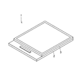
- FIG. 1 is a perspective view of a display device 1 according to an embodiment of the present invention.
- the display device 1 has a TFT (Thin Film Transistor) substrate 2.
- the display device 1 may have an opposing substrate 3 facing the TFT substrate 2.
- the opposing substrate 3 may not be provided.
- the display device 1 has a plurality of pixels arranged in the vertical direction and the horizontal direction.
- the display device 1 preferably includes a plurality of pixels that respectively emit light in different colors.
- the color of the pixel is, for example, three colors of red, green and blue, and four colors of red, green, blue and white.
- the color of the pixel may include cyan, magenta and yellow.
- FIG. 2 is a view showing an example of a circuit formed in each pixel. This circuit is formed on the TFT substrate 2.
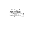
- 3A and 3B schematically show an example of the light emitting transistor 20 described later, FIG. 3A is a plan view, and FIG. 3B is a cross-sectional view taken along line bb of FIG. 3A.
- the display device 1 has a plurality of scanning lines 51 and a plurality of signal lines 52.
- the scanning line 51 and the signal line 52 are orthogonal to each other.
- the scan line 51 is connected to a scan line drive circuit (not shown), and a scan signal is applied from the scan line drive circuit.
- the signal line 52 is connected to a signal line drive circuit (not shown), and a signal (voltage) corresponding to the gradation value of each pixel is applied from the signal line drive circuit.
- the display device 1 includes a first wiring 53 and a second wiring 54 which is set to a potential different from that of the first wiring 53. In one example, the potential of the first wiring 53 and the potential of the second wiring 54 are constant. Although the first wiring 53 and the second wiring 54 in FIG. 2 extend in the direction along the scanning line 51, the extending direction of the wirings 53 and 54 is not limited thereto.
- Each pixel has a selection transistor 10 and a light emitting transistor 20.
- the selection transistor 10 has a gate electrode 14 connected to the scanning line 51, a first source / drain electrode 12 connected to the signal line 52, and a second source / drain electrode 13.
- the light emitting transistor 20 has a gate electrode 21 connected to the second source / drain electrode 13 of the selection transistor 10. A voltage corresponding to the gradation value of the pixel is applied to the gate electrode 21 through the second source / drain electrode 13.
- the gate electrode 21 may be directly connected to the second source / drain electrode 13 or may be indirectly connected to the second source / drain electrode 13 through another circuit element.
- the light emitting transistor 20 includes a first electrode 22 electrically connected to the first wiring 53 and a second electrode 23 electrically connected to the second wiring 54.
- the first wiring 53 and the first electrode 22 may be formed in different conductive layers, or the first wiring 53 and the first electrode 22 may be formed in the same conductive layer.
- first wiring 53 and the first electrode 22 are formed in the same conductive layer, a part of the first wiring 53 may function as the first electrode 22.
- the second wiring 54 and the second electrode 23 may be formed in different conductive layers, and the second wiring 54 and the second electrode 23 may be formed in the same conductive layer.
- a part of the second wiring 54 may function as the second electrode 23.
- the light emitting transistor 20 has a channel layer 24 containing quantum dots, and the carriers flowing in the channel layer 24 cause the quantum dots to emit light.
- Quantum dots are semiconductor particles capable of confining charge in dot-like regions.
- the quantum dot generally has a particle diameter of about several nm to about 20 nm, which is composed of about several hundreds to several thousands of atoms.
- the quantum dot has, for example, a core-shell structure having semiconductor particles (core portion) and a shell portion covering the surface of the core portion and having a band gap energy larger than that of the core portion.
- the fine particles in the core portion those that emit visible light by recombination of electrons and holes are used.
- the material of the core portion include II-VI group semiconductor compounds (for example, MgS, MgSe, MgTe, CaS, CaSe, CaTe, SrS, SrSe, SrTe, BaS, BaSe, BaTe, ZnS, ZnSe, ZnTe , CdS, CdSe, CdTe, HgS, HgSe and HgTe) and III-V semiconductor compounds (eg, AlN, AlP, AlAs, AlSb, GaAs, GaP, GaN, GaSb, InN, InAs, InP, InSb, TiN, Semiconductor crystals containing TiP, TiAs and TiSb), Group IV semiconductors (eg, Si, Ge and Pb) semiconductor compounds or semiconductors can be used.
- II-VI group semiconductor compounds for example, MgS, MgS
- a semiconductor crystal containing a semiconductor compound containing three or more elements such as InGaP may be used as a material of the core portion.
- a semiconductor material having a band gap energy larger than that of the core portion it is desirable to use a semiconductor material having a band gap energy larger than that of the core portion. By using such a material, charge can be effectively confined in the core portion of the quantum dot.
- core-shell structure for example, CdSe / ZnS, CdSe / ZnSe, CdSe / CdS, CdTe / CdS, InP / ZnS, Gap / ZnS, Si / ZnS, InN / GaN, InP / CdSSe InP / ZnSeTe, InGaP / ZnSe, InGaP / ZnS, Si / AlP, InP / ZnSTe, InGaP / ZnSTe, InGaP / ZnSSe, and the like.
- a well-known method can be used as a preparation method of a quantum dot.
- a gas phase synthesis method a liquid phase synthesis method, a solid phase synthesis method, a vacuum synthesis method or the like can be used.
- synthesis methods such as hot soap method, reverse micelle method, solvothermal method, hydrothermal method, coprecipitation method and the like can be used.
- Quantum dots emit light of a color (wavelength) according to their size (particle diameter). Therefore, the size of the quantum dot contained in the channel layer 24 is controlled such that the quantum dot emits visible light. Specifically, the size of the quantum dot of the channel layer 24 is controlled to emit, for example, red light, green light, and blue light.
- the channel layer 24 may have a host material in which quantum dots are mixed.
- a host material the organic host material used by organic EL can be utilized.
- triphenylamine derivatives, arylamine dielectrics, oxadiazole derivatives, anthracene derivatives, carbazole derivatives, phenanthrolines and the like can be used as the host material.
- the triphenylamine derivative is, for example, N, N′-bis- (3-methylphenyl) -N, N′-bis- (phenyl) -benzidine (TPD), 4,4 ′, 4 ′ ′-tris (3-Methylphenylphenylamino) triphenylamine (MTDATA)
- the arylamine dielectric is, for example, bis (N- (1-naphthyl-N-phenyl) benzidine) ( ⁇ -NPD).
- the azole derivative is, for example, (2- (4-biphenylyl) -5- (4-tert-butylphenyl) -1,3,4-oxadiazole) (PBD)
- Anthracene derivative is, for example, 9, 9, 10-di-2-naphthylanthracene (DNA) is a carbazole derivative such as 4,4-N, N'-dicarbazole-biphenyl (CBP), 1,4-bis 2, 2-Diphenylvinyl) benzene (DPVBi)
- Phenanthrolines are, for example, vasocuproin, bathophenanthroline etc.
- electron transport materials such as phthalocyanine derivatives, polythiophene derivatives and porphyrin derivatives are used as host materials It is also good.
- the gate electrode 21 is formed on the opposite side to the electrodes 22 and 23 across the channel layer 24.
- the gate electrode 21 is formed below the channel layer 24, and the first electrode 22 and the second electrode 23 are formed below the channel layer 24.
- the first electrode 22 is connected to one edge of the channel layer 24 and the second electrode 23 is connected to the opposite edge of the channel layer 24.
- the channel layer 24 is a rectangle elongated in the channel width direction (Dw direction in FIG. 3A).
- the channel width of the channel layer 24 corresponds to the size of the pixel (S in FIG. 3A).
- the gate electrode 21 is formed on the insulating layer 31.
- the selection transistor 10 is formed in a layer lower than the insulating layer 31.
- the insulating layer 31 is formed of, for example, an acrylic resin, as described later, and functions as a planarizing film having a flat surface.
- the gate electrode 21 is covered with an insulating layer 32.
- the insulating layer 32 is formed of, for example, SiO2.
- the channel layer 24 is formed on the insulating layer 32.
- the channel layer 24 may be covered by an insulating layer 33, as shown in FIGS. 3A and 3B.
- the first electrode 22 and the second electrode 23 may be connected to the channel layer 24 through through holes.
- the first electrode 22 and the second electrode 23 may be formed directly on the channel layer 24.
- the gate electrode 21 As materials of the gate electrode 21, the first electrode 22, and the second electrode 23, metals such as aluminum, silver, copper, and nickel can be used. A transparent conductive material such as ITO or IZO may be used as the material of these electrodes.
- the gate electrode 21 When the display device 1 is a top emission type, the gate electrode 21 has a reflective surface that reflects light. The reflective surface is formed of, for example, a metal such as aluminum or silver.
- the gate electrode 21 is formed of the above-described transparent conductive material.
- the gate electrode 21 may have a plurality of conductive layers.
- the material of the first electrode 22 and the material of the second electrode 23 may be different from each other. By using different materials for the first electrode 22 and the second electrode 23, the work function of the first electrode 22 and the work function of the second electrode 23 can be made different, and as a result, carrier injection into the channel layer 24 can be achieved. Efficiency can be improved.
- the channel layer 24 is composed of the above-described quantum dots and a host material.
- the channel layer 24 includes a region (first region 24 a) in contact with the first electrode 22, a region (second region 24 b) in contact with the second electrode 23, and the first region 24 a and And a third area 24c which is an area between the second areas 24b.
- At least one of the first region 24a and the second region 24b may have a composition different from that of the third region 24c.
- the first region 24a and the second region 24b may be doped with ions (eg, lithium ion, potassium ion, argon ion, nitrogen ion or hydrogen ion) as impurities. By doing this, the carrier injection efficiency from the first electrode 22 or the second electrode 23 can be increased.
- the impurities do not necessarily have to be such ions.
- each pixel may be provided with a storage capacitor 26 connected to the second source / drain electrode 13 of the selection transistor 10.
- a voltage corresponding to the gradation value of the pixel is applied to the signal line 52 when the selection transistor 10 is in the on state, charges are stored in the storage capacitor 26.
- the other electrode of the storage capacitor 26 is connected to, for example, the first wiring 53.
- the storage capacitor 26 is formed, for example, in a layer lower than the insulating layer 31 shown in FIGS. 3A and 3B.
- the light emitting transistor 20 can operate as follows. Due to the potential difference between the first electrode 22 and the second electrode 23, for example, electrons are injected from the first electrode 22 to the channel layer 24, and holes are injected from the second electrode 23 to the channel layer 24.
- the potential of the gate electrode 21 is set so that the injected carriers (electrons and holes) move toward the vicinity of the center of the channel layer 24 (near the center of the channel). Carriers are considered to move in the host material or move between adjacent quantum dots by tunneling phenomenon or hopping phenomenon. Electrons and holes are taken into the quantum dot near the center of the channel layer 24 and recombined to generate excitons.
- the quantum dots emit light.
- the carrier transport amount of the channel layer 24 is considered to depend not only on the potential difference between the first electrode 22 and the second electrode 23, but also on the potential of the gate electrode 21. That is, the channel layer 24 has high insulation when no voltage is applied to the gate electrode 21. By applying a voltage to the gate electrode 21, it is considered that the electrical conductivity of the channel layer 24 can be increased.
- the electron density of the quantum dot depends on the potential of the gate electrode 21.
- the movement of electrons between quantum dots is considered to depend on the electron density of quantum dots. For example, when the electron density in each quantum dot is high, the electron is confined in the quantum dot by the interaction with the electron of the next quantum dot and can not move between the quantum dots. For these reasons, the recombination probability of electrons and holes can be controlled by the potential of the gate electrode 21, and the emission luminance can be controlled.
- the concentration of quantum dots in the host material may not necessarily be uniform in the channel layer 24. That is, the concentration of quantum dots in the host material may have a slope in the direction of the channel length. For example, the concentration of the quantum dots may be thinner in the vicinity of the center of the channel layer 24 than in other portions (a portion near the first electrode 22 and a portion near the second electrode 23). This can suppress the localization of the light emitting region in the channel layer 24 near the center.
- the light emitting transistor 20 can operate as follows.
- the channel layer 24 has, for example, an electron transporting property and the first electrode 22 is set to a potential lower than that of the second electrode 23
- electrons are injected from the first electrode 22 into the channel layer 24.
- the injected electrons are transported toward the second electrode 23. It is thought that the quantum dot is excited by the collision between the electron and the quantum dot in the transport process of the electron, or the electron enters the high energy level in the quantum dot in the transport process of the electron. Therefore, the quantum dot emits light due to deactivation.
- the quantum dots can emit light. Electrons and holes are taken into the quantum dot near the center of the channel layer 24 and recombined to generate excitons. As a result, the quantum dots emit light.
- the carrier transport amount of the channel layer 24 is considered to depend not only on the potential difference between the first electrode 22 and the second electrode 23, but also on the potential of the gate electrode 21. That is, the channel layer 24 has high insulation when no voltage is applied to the gate electrode 21.
- the electrical conductivity of the channel layer 24 can be increased.
- the electron density of the quantum dot depends on the potential of the gate electrode 21.
- the movement of electrons between quantum dots is considered to depend on the electron density of quantum dots. For example, when the electron density in each quantum dot is high, the electron is confined in the quantum dot by the interaction with the electron of the next quantum dot and can not move between the quantum dots. For these reasons, the recombination probability of electrons and holes can be controlled by the potential of the gate electrode 21, and the emission luminance can be controlled.
- the selection transistor 10 When an on voltage (scan signal) is applied to the scan line from the scan line drive circuit, the selection transistor 10 is turned on. At this time, a voltage (gradation signal) corresponding to the gradation value of the pixel is applied to the signal line from the signal line driver circuit. As a result, a voltage corresponding to the gradation value is applied to the gate electrode 21 of the light emitting transistor 20 through the selection transistor 10. As a result, carriers according to the gradation value flow in the channel layer 24.
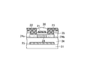
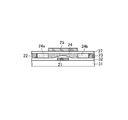
- FIG. 4 is a cross-sectional view showing a modification of the light emitting transistor 20.
- the light emitting transistor 20 may have the auxiliary electrode 25 on the opposite side to the gate electrode 21 with the channel layer 24 interposed therebetween.
- the auxiliary electrode 25 is set to the same potential as the gate electrode 21.
- the transport amount of carriers and the carrier density in the channel layer 24 can be easily controlled, and the operation of the light emitting transistor 20 can be stabilized or the temporal change in the operation of the light emitting transistor 20 can be suppressed. it can.
- metals such as aluminum, silver, copper, nickel and the like can be used.
- a transparent conductive material such as ITO or IZO may be used.
- the auxiliary electrode 25 is formed of a transparent conductive material.
- the auxiliary electrode 25 has a reflective surface that reflects light.
- the reflective surface is formed of, for example, a metal such as aluminum or silver.
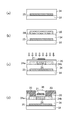
- FIG. 5 is a view showing an example of a manufacturing process of the light emitting transistor 20.
- the gate electrode 21 is formed on the insulating layer 31.
- the gate electrode 21 can be formed by a sputtering method, an evaporation method, or the like.
- the gate electrode 21 is covered with an insulating layer 32.
- the channel layer 24 is formed on the insulating layer 32.
- the channel layer 24 is formed of the above-described material.
- the channel layer 24 can be formed by, for example, a coating method or a transfer method. In the coating method, a coating solution containing quantum dots and a host material is coated on the insulating layer 32.
- a channel layer formed on a film by a coating method or a vapor deposition method is attached on the insulating layer 32, and the channel layer is transferred to the insulating layer 32. Then, the channel layer 24 is covered with the insulating layer 33.
- the auxiliary electrode 25 is formed on the insulating layer 33.
- the auxiliary electrode 25 can also be formed by sputtering, evaporation, or the like.
- nitrogen ions or hydrogen ions are implanted into the first region 24 a and the second region 24 b of the channel layer 24.
- the auxiliary electrode 25 may function as a mask, or a dedicated mask may be used.
- through holes are formed in the insulating layer 33.
- the through holes are formed at positions corresponding to the first region 24 a of the channel layer 24 and at positions corresponding to the second region 24 b.
- the first electrode 22 and the second electrode 23 are formed on the insulating layer 33, and these electrodes 22 and 23 are connected to the channel layer 24 through the through holes.
- the electrodes 22 and 23 can be formed, for example, by sputtering or vapor deposition.
- a mask is disposed on the insulating layer 33 in the process of FIG. Nitrogen ions or hydrogen ions are implanted into the channel layer 24.
- FIG. 6 is a cross-sectional view showing a modification of the light emitting transistor 20.
- the gate electrode 21 may be formed on the same side as the first electrode 22 and the second electrode 23 with respect to the channel layer 24.
- the channel layer 24 is covered by the insulating layer 35, and the gate electrode 21 is formed on the insulating layer 35.
- the insulating layer 35 is formed of, for example, SiO2.
- the gate electrode 21 is covered by an insulating layer 36.
- the insulating layer 36 is formed of SiO 2 or SiN.
- the first electrode 22 and the second electrode 23 are formed on the insulating layer 36.
- the first electrode 22 and the second electrode 23 are connected to the channel layer 24 through through holes formed in the insulating layers 35 and 36.
- the auxiliary electrode 25 is provided on the opposite side of the channel layer 24 to the gate electrode 21. That is, the auxiliary electrode 25 may be formed below the channel layer 24, and the insulating layer 34 may be formed between the channel layer 24 and the auxiliary electrode 25.
- the insulating layer 34 is also formed of, for example, SiO2.
- the auxiliary electrode 25 is formed on the above-described insulating layer 31 which functions as a planarization film. The auxiliary electrode 25 may not necessarily be formed. Also in the example of FIG. 6, at least one of the first region 24a (the region in which the first electrode 22 is in contact) and the second region 24b (the region in which the second electrode 23 is in contact) of the channel layer 24.
- the region of may have a different composition than the third region 24c, which is the region between them.
- ions for example, nitrogen ions or hydrogen ions
- the impurities do not necessarily have to be such ions.
- FIG. 7 is a view showing an example of a manufacturing process of the light emitting transistor 20 shown in FIG.
- the auxiliary electrode 25 is formed on the insulating layer 31.
- the auxiliary electrode 25 can also be formed by a sputtering method, a vapor deposition method, or the like. Then, the auxiliary electrode 25 is covered with the insulating layer 34.
- the channel layer 24 is formed on the insulating layer 34.
- the channel layer 24 can be formed by, for example, a coating method, a transfer method, or the like, as in the example of FIG. Then, the channel layer 24 is covered with the insulating layer 35.
- FIG. 7A the auxiliary electrode 25 is formed on the insulating layer 31.
- the auxiliary electrode 25 can also be formed by a sputtering method, a vapor deposition method, or the like. Then, the auxiliary electrode 25 is covered with the insulating layer 34.
- the channel layer 24 is formed on the insulating layer 34.
- the gate electrode 21 is formed on the insulating layer 35.
- the gate electrode 21 can be formed by, for example, a sputtering method, a vapor deposition method, or the like. Thereafter, nitrogen ions or hydrogen ions are implanted into the first region 24 a and the second region 24 b of the channel layer 24. In this step, the gate electrode 21 may function as a mask or a dedicated mask may be used.
- the gate electrode 21 is covered with the insulating layer 36. Then, through holes are formed in the insulating layers 35 and 36. The through holes are formed at positions corresponding to the first region 24 a of the channel layer 24 and at positions corresponding to the second region 24 b.
- the first electrode 22 and the second electrode 23 are formed on the insulating layer 36, and these electrodes 22 and 23 are connected to the channel layer 24 through the through holes.
- the electrodes 22 and 23 can be formed by a sputtering method, a vapor deposition method, or the like.
- the channel layer 24 is formed on the insulating layer 31, and then the steps shown in FIGS. 7 (c) and 7 (d) are performed.
- FIG. 8 is a cross-sectional view showing still another modified example of the light emitting transistor 20.
- the gate electrode 21, the first electrode 22, and the second electrode 23 may be formed below the channel layer 24.
- the gate electrode 21 is formed on the insulating layer 31 and covered with the above-described insulating layer 32.
- the first electrode 22 and the second electrode 23 are formed on the insulating layer 32.
- the channel layer 24 is formed on the insulating layer 32.
- One edge of the channel layer 24 is formed on the first electrode 22, and the opposite edge of the channel layer 24 is formed on the second electrode 23.
- Channel layer 24 is covered with insulating layer 37.
- the auxiliary electrode 25 may be formed on the insulating layer 37.
- the auxiliary electrode 25 may not necessarily be formed.
- FIG. 9 is a cross-sectional view showing still another modified example of the light emitting transistor 20.
- the gate electrode 21, the first electrode 22, and the second electrode 23 are formed below the channel layer 24 as in FIG. 8.
- the first region 24a (the region in which the first electrode 22 is in contact) and the second region 24b (the region in which the second electrode 23 is in contact) of the channel layer 24 are
- the third region 24c which is an intermediate region, has a different composition.
- ions for example, nitrogen ions or hydrogen ions
- the impurities do not necessarily have to be such ions.
- each of the electrodes 22 and 23 may be provided with a taper angle. That is, a slope may be provided on the contact surface between the electrodes 22 and 23 and the channel layer 24. By doing this, the contact area can be further expanded, and the light emission efficiency can be improved by surface reflection.
- the edge of the channel layer 24 may be disposed on the upper side of the electrodes 22 and 23 according to FIG.
- FIG. 10 and 11 are diagrams showing an example of the TFT substrate 2 provided in the display device 1.
- FIG. 10A is a plan view.
- FIG. 10B is an enlarged view of FIG. 10A.
- FIG. 11 is a cross-sectional view taken along line XI-XI shown in FIG. 10B.
- the TFT substrate 2 has a substrate 40 formed of glass, resin or the like.
- the substrate 40 may be transparent or opaque.
- the substrate 40 is a transparent substrate.
- the select transistor 10 is formed on the substrate 40.
- the semiconductor layer 11 is formed on the substrate 40.
- the semiconductor layer 11 is, for example, amorphous silicon, but polycrystalline silicon, an organic semiconductor, a metal oxide semiconductor, or the like may be used as the semiconductor layer 11.
- the base layer 41 of SiO 2 or SiN may be formed on the substrate 40, and the semiconductor layer 11 may be formed on the base layer 41.
- the semiconductor layer 11 is covered with the insulating layer 42, and the gate electrode 14 is formed on the insulating layer 42.
- the scan line 51 may be formed on the same conductive layer as the semiconductor layer 11.
- the gate electrode 14 is covered with an interlayer insulating layer 43, and the first source / drain electrode 12 and the second source / drain electrode 13 are formed on the interlayer insulating layer 43.
- the source / drain electrodes 12 and 13 are connected to the semiconductor layer 11 through through holes.
- the source / drain electrodes 12 and 13 are covered by a passivation film 44.
- the laminated structure of the selection transistor 10 is not limited to that shown in FIG.
- the semiconductor layer 11 may be formed on the upper side of the gate electrode 14.
- the insulating layer 31 described above is formed on the passivation film 44.
- the insulating layer 31 functions as, for example, a planarizing film having a planarized surface.
- the planarization film is formed of, for example, an acrylic resin.
- the light emitting transistor 20 is formed on the insulating layer 31.
- the gate electrode 21 is formed on the insulating layer 31 as in the example of FIGS. 3A and 3B.
- the gate electrode 21 is connected to the second source / drain electrode 13 of the selection transistor 10 through the through hole. Through holes are formed in the insulating layer 31 and the passivation film 44.
- a channel layer 24 including quantum dots is formed on the upper side of the gate electrode 21.
- the gate electrode 21 is covered by the insulating layer 32, and the channel layer 24 is formed on the insulating layer 32.
- the channel layer 24 is separated between two adjacent pixels. That is, the channel layer 24 of one pixel and the channel layer 24 of the other pixel are not connected. As shown in FIG. 11, the gate electrode 21 may have a size larger than that of the channel layer 24.
- the channel layer 24 may be present inside the outer peripheral edge of the gate electrode 21 in plan view. This can suppress the occurrence of irregularities in the channel layer 24.
- the display device 1 is, for example, a top emission type.
- the gate electrode 21 has a reflective surface as described above.
- the entire gate electrode 21 may be formed of a material that reflects light, or the gate electrode 21 may be formed of a plurality of conductive layers, and a portion of the conductive layer may be formed of a material that reflects light.
- the display device 1 has a plurality of pixels that emit light in different colors.
- the display device 1 includes three pixels of red pixel (R), green pixel (G), and blue pixel (B).
- the emission wavelength (color) of the quantum dot depends on the size of the quantum dot. Therefore, in the example of the display device 1, the channel layers 24 of the plurality of pixels each include the plurality of types of quantum dots having different sizes.
- the channel layer 24 of the first color pixel for example, red pixel (R)
- the channel layer 24 of the second color pixel for example, green pixel (G)
- the third color pixel The channel layer 24 of (for example, the blue pixel (B)) includes three types of quantum dots having different sizes.
- the size of the quantum dot may be the same for multiple pixels of different colors.
- quantum dots of a first color pixel eg, red pixel (R)
- quantum dots of a second color pixel eg, green pixel (G)
- a third color pixel eg, Blue pixels (B)
- a color filter or a color conversion filter may be used to realize the color of each pixel.
- the color filter or the color conversion filter may be formed on the counter substrate 3 or may be formed on the TFT substrate 2.
- the channel layer 24 of each pixel may include multiple types of quantum dots of different sizes.
- the channel layer 24 may have a plurality of layers formed of quantum dots of different sizes. That is, the channel layer 24 may have a layer of quantum dots having a first size, a layer of quantum dots having a second size, and a layer of quantum dots having a third size.
- the number of layers of quantum dots may be more or less than three.
- the first electrode 22 and the second electrode 23 are formed on the channel layer 24.
- the first electrode 22 is electrically connected to one edge of the channel layer 24 and the second electrode 23 is electrically connected to the opposite edge of the channel layer 24.
- the first electrode 22, the second electrode 23, and the channel layer 24 may be covered by a protective film 49 as shown in FIG. 11.
- the counter substrate 3 (FIG. 1) may be disposed on the upper side of the protective film 49.
- an insulating layer 38 having an opening in each pixel may be formed on the insulating layer 32.
- the position of the opening of the insulating layer 38 corresponds to the position of the gate electrode 21.
- the channel layer 24 is formed inside the opening of the insulating layer 38, and faces the gate electrode 21 with the insulating layer 32 interposed therebetween.
- an acrylic resin may be used as the material of the insulating layer 38.
- the first electrode 22 and the second electrode 23 are formed on the insulating layer 38. A portion of the electrodes 22, 23 is located on the channel layer 24 and connected to the channel layer 24.
- the first wiring 53 and the second wiring 54 are formed on the TFT substrate 2.
- the wires 53 and 54 are formed on the insulating layer 38.
- a part of the first wiring 53 is the first electrode 22, and a part of the second wiring 54 is the second electrode 23.
- the layers in which the wires 53 and 54 are formed are not limited to those shown in FIG.
- the first wire 53 and the second wire 54 may be formed in a layer below the channel layer 24 as described later.
- a plurality of pixels of different colors are regularly arranged in the horizontal direction.
- Each pixel is rectangular, and the width of the pixel in the vertical direction is larger than the width of the pixel in the horizontal direction (in FIG. 10A and FIG. 10B, the V direction is the vertical direction and the H direction is the horizontal direction).
- the channel layer 24 is also rectangular according to the shape of the pixel.
- the first electrode 22 is connected to one edge of the channel layer 24 in the vertical direction, and the second electrode 23 is connected to the opposite edge of the channel layer 24 in the vertical direction.
- first electrode 22 and the second electrode 23 are provided are not limited to the examples of FIGS. 10A and 10B.
- the first electrode 22 may be connected to one edge of the channel layer 24 in the horizontal direction
- the second electrode 23 may be connected to the opposite edge of the channel layer 24 in the horizontal direction. That is, when the width of the channel layer 24 in the first direction is larger than the width in the second direction orthogonal to the first direction, the first electrode 22 and the second electrode 23 are opposite to each other in the second direction. It may be located at
- the TFT substrate 2 has a plurality of pixel rows L (in FIG. 10A and FIG. 10B, subscripts n to n + 3 are attached to each pixel row L).
- the plurality of pixels are aligned in one direction in each pixel row L.
- Each pixel row L is composed of a plurality of pixels arranged in the horizontal direction.
- the plurality of pixel rows L are arranged in the vertical direction.
- a plurality of pixels of different colors in the example of FIGS. 10A and 10B, red pixels (R), green pixels (G), and blue pixels (B)
- pixels of the same color may be arranged in each pixel row.
- the first wiring 53 includes a first extending portion 53a which is formed between two adjacent pixel rows L and extends in the horizontal direction.
- the first extending portion 53 a of the first wiring 53 is connected to the channel layers 24 of a plurality of pixels included in two adjacent pixel rows L. That is, the first extending portion 53 a of the first wiring 53 configures the first electrode 22 of the pixel included in the two adjacent pixel rows L.
- the first wiring 53 includes a plurality of first extending portions 53a. Further, the first wiring 53 includes a second extending portion 53 b extending in the vertical direction and connecting the plurality of first extending portions 53 a.
- the second wiring 54 also includes a first extending portion 54a formed between two adjacent pixel rows L.
- the first extending portion 54 a of the second wiring 54 is connected to the channel layer 24 of the pixel included in the two adjacent pixel rows L. That is, the first extending portion 54 a of the second wiring 54 configures the second electrodes 23 of a plurality of pixels included in two adjacent pixel rows L.
- the second wiring 54 includes a plurality of first extending portions 54 a.
- the second wiring 54 includes a second extending portion 54 b extending in the vertical direction and connecting the plurality of first extending portions 54 a.
- the first extending portions 53 a of the first wires 53 and the first extending portions 54 a of the second wires 54 are alternately arranged in the vertical direction.
- the second extending portion 53 b of the first wiring 53 and the second extending portion 54 b of the second wiring 54 are located on the opposite side to each other across the plurality of pixels aligned in the horizontal direction.
- the layouts of the wires 53 and 54 are not necessarily limited to those shown in FIGS. 10A and 10B.
- the voltage may not be applied simultaneously to the plurality of first extending portions 53a and 54a aligned in the vertical direction.
- voltages may be sequentially applied to the plurality of first extending portions 53a and 54a in a predetermined method for each pixel row. In this case, each of the wires 53 and 54 may not include the second extending portions 53 b and 54 b.
- the storage capacitor 26 is formed in each pixel.
- the storage capacitor 26 has two opposing electrodes 26a, 26b.
- the first electrode 26 a is formed, for example, in the same layer as the semiconductor layer 11 of the selection transistor 10, as shown in FIG. 11.
- the second electrode 26 b is formed, for example, on the insulating layer 42.
- the second electrode 26 b may be formed on the interlayer insulating layer 42 in the same manner as the source / drain electrodes 12 and 13.
- One of the electrodes 26a and 26b is connected to the second source / drain electrode 13 of the selection transistor 10, and the other electrode is connected to, for example, the first wiring 53 via a through hole.
- FIG. 12 is a cross-sectional view showing a modification of the TFT substrate 2.
- the same reference numerals are given to the same parts as those described above.
- the light emitting transistor 20 of each pixel may have an auxiliary electrode 25 located on the opposite side of the channel layer 24 to the gate electrode 21.
- the insulating layer 39 is formed on the channel layer 24.
- the auxiliary electrode 25 is formed on the insulating layer 39.
- the auxiliary electrode 25 is connected to the gate electrode 21 via, for example, a through hole (not shown).
- FIG. 13 and 14 are cross-sectional views showing still another modified example of the TFT substrate 2.
- FIG. 13A is a plan view.
- FIG. 13B is an enlarged view of FIG. 13A.
- FIG. 14 is a cross-sectional view taken along line XIV-XIV shown in FIG. 13B.
- the same reference numerals are given to the same parts as those described above.
- the first wiring 53 and the second wiring 54 are formed in a layer below the channel layer 24. Specifically, the first wiring 53 and the second wiring 54 are formed on the passivation film 44 and covered by the insulating layer 31. The first electrode 22 and the second electrode 23 are respectively connected to the first wiring 53 and the second wiring 54 through the through holes.
- the first wiring 53 includes the first extending portion 53 a formed between two adjacent pixel rows L. The first extending portion 53 a is connected to the first electrode 22 through through holes formed in the insulating layers 31, 32 and 38.
- the second wiring 54 has a first extending portion 54 a formed between two adjacent pixel rows L.
- the first extending portion 54 a is connected to the second electrode 23 through through holes formed in the insulating layers 31, 32 and 38. Also in the examples of FIGS. 13A, 13B, and 14, the auxiliary electrode 25 may be formed on the opposite side to the gate electrode 21 with the channel layer 24 interposed therebetween.
- FIG. 15 is a cross-sectional view showing still another modified example of the TFT substrate 2.
- the same reference numerals are given to the same parts as those described above.
- the insulating layer 38 is formed on the insulating layer 31.
- the insulating layer 38 has an opening at each pixel as described above.
- the gate electrode 21 and the channel layer 24 are formed inside the opening of the insulating layer 38.
- the insulating layer 32 is formed on the gate electrode 21, and the channel layer 24 is formed on the insulating layer 32.
- the insulating layer 38 has an inclined surface 38 a on the inner peripheral surface of the opening.
- the outer peripheral portion 21 a of the gate electrode 21 is formed on the inclined surface 38 a of the insulating layer 38. Therefore, the outer peripheral portion 21a of the gate electrode 21 is inclined obliquely upward toward the center of each pixel.
- the gate electrode 21 has a reflective surface which reflects the light from the channel layer 24. According to the outer peripheral portion 21 a of the gate electrode 21, light exiting from the channel layer 24 and traveling in the direction along the substrate 40 is reflected by the outer peripheral portion 21 a of the gate electrode 21 and exits from the surface of the display device 1.
- each pixel includes an auxiliary electrode 25 located on the opposite side of the channel layer 24 to the gate electrode 21.
- the auxiliary electrode 25 may not necessarily be formed.
- the laminated structure of the light emitting transistor 20 is not limited to that shown in FIG. 11, FIG. 12, FIG. 14, and FIG.
- the gate electrode 21, the first electrode 22, and the second electrode 23 may be formed on the same side with respect to the channel layer 24.
- the gate electrode 21 may be formed on the upper side of the channel layer 24.
- the gate electrode 21 may be covered by an insulating layer, and the first electrode 22 and the second electrode 23 may be formed on the upper side of the insulating layer.
Landscapes
- Engineering & Computer Science (AREA)
- Physics & Mathematics (AREA)
- Optics & Photonics (AREA)
- Chemical & Material Sciences (AREA)
- Crystallography & Structural Chemistry (AREA)
- Inorganic Chemistry (AREA)
- Nanotechnology (AREA)
- Microelectronics & Electronic Packaging (AREA)
- Electroluminescent Light Sources (AREA)
- Devices For Indicating Variable Information By Combining Individual Elements (AREA)
- Thin Film Transistor (AREA)
- Led Devices (AREA)
Abstract
画素には、選択トランジスタ(10)と発光トランジスタ(20)とが設けられる。選択トランジスタ(10)は、走査線(51)に接続されているゲート電極(14)と、信号線(52)に接続されている第1のソース・ドレイン電極(12)と、第2のソース・ドレイン電極(13)とを有している。発光トランジスタ(20)は、選択トランジスタ(10)の第2のソース・ドレイン電極(13)に接続されているゲート電極(21)と、第1の配線(53)に接続されている第1の電極(22)と、第2の配線(54)に接続されている第2の電極(23)と、量子ドットを含んでいるチャネル層(24)とを有している。発光トランジスタ(20)は、チャネル層(24)を流れるキャリアにより量子ドットを発光させる。
Description
本発明は量子ドットを利用する表示装置に関する。
ドット状の領域に電荷を閉じ込めることのできる量子ドット(量子箱)が知られている。量子ドットは、一般的に、数百~数千個程度の原子から構成された微粒子である。特表2010-520603号公報(以下において文献1と称する)は、量子ドットを用いたアクティブマトリックス型表示装置を開示している。この表示装置は、各画素に、量子ドットを含む発光層を2つの電極で挟む無機発光ダイオードを有している。また、文献1の表示装置は、パワートランジスタと、選択トランジスタと、保持容量(文献1においてストレージキャパシタ)とを各画素に有している。パワートランジスタは無機発光ダイオードに供給する電流を制御する。選択トランジスタは、走査線(文献1においてセレクトライン)と信号線(文献1においてデータライン)とに接続され、信号線から受ける信号に応じた電圧をパワートランジスタのゲートに加える。保持容量はパワートランジスタのゲートの電圧を維持する。特開2010-209141号公報には、量子ドットを含む発光層を2つの電極で挟む発光デバイスが開示されている。
近年、表示装置の高精細化が進んでいる。表示装置をさらに高精細化しようとすると、1つの画素のサイズがますます小さくなるので、多くの回路素子(上述のトランジスタやキャパシタ)を各画素に設けることが難しくなる。
本発明の目的は、量子ドットを利用し、且つ、各画素に設けられる回路素子の数を低減できる表示装置を提供することにある。
本発明に係る表示装置は、複数の画素と、走査線と、信号線と、第1の配線と、第2の配線と、を有している。前記複数の画素のうち少なくとも1つの画素は、前記走査線に接続されているゲート電極と、前記信号線に接続されている第1のソース・ドレイン電極と、第2のソース・ドレイン電極とを有している選択トランジスタと、前記選択トランジスタの前記第2のソース・ドレイン電極を通して前記少なくとも1つの画素の階調値に応じた電圧が加えられるゲート電極と、前記第1の配線に接続されている第1の電極と、前記第2の配線に接続されている第2の電極と、量子ドットを含んでいるチャネル層とを有し、前記チャネル層を流れるキャリアにより前記量子ドットを発光させる発光トランジスタとを有している。
以下、本発明の一実施形態について説明する。本明細書の開示は本発明の一例にすぎず、本発明の主旨を保った適宜変更であって当業者が容易に想到し得るものは本発明の範囲に含まれる。また、図で示す各部の幅、厚さ及び形状等は模式的に表される場合があり、それらは本発明の解釈を限定するものではない。
図1は本発明の実施形態に係る表示装置1の斜視図である。表示装置1はTFT(Thin Film Transistor)基板2を有している。表示装置1はTFT基板2と対向する対向基板3を有してもよい。対向基板3は設けられていなくてもよい。表示装置1は、垂直方向と水平方向に並んでいる複数の画素を有している。表示装置1は、互いに異なる色でそれぞれ発光する複数の画素を含んでいることが好ましい。画素の色は、例えば赤、緑、及び青の3色や、赤、緑、青、白の4色などである。画素の色として、シアン、マゼンタ、イエローが含まれてもよい。
図2は各画素に形成される回路の例を示す図である。この回路はTFT基板2に形成されている。図3A及び図3Bは、後述する発光トランジスタ20の一例の概略を示す図であり、図3Aは平面図であり、図3Bは図3Aのb-b線での断面図である。
図2に示すように、表示装置1は、複数の走査線51と複数の信号線52とを有している。走査線51と信号線52は互いに直交している。走査線51は図示しない走査線駆動回路に接続され、走査線駆動回路から走査信号が加えられる。信号線52は図示しない信号線駆動回路に接続され、信号線駆動回路から各画素の階調値に応じた信号(電圧)が加えられる。表示装置1は、第1配線53と、第1配線53とは異なる電位に設定されている第2配線54とを有している。一例では、第1配線53の電位と第2配線54の電位は一定である。図2の第1配線53と第2配線54は、走査線51に沿った方向に伸びているが、これらの配線53、54の延伸方向はこれに限られない。
各画素は選択トランジスタ10と発光トランジスタ20とを有している。選択トランジスタ10は、走査線51に接続されているゲート電極14と、信号線52に接続されている第1ソース・ドレイン電極12と、第2ソース・ドレイン電極13とを有している。
発光トランジスタ20は、選択トランジスタ10の第2ソース・ドレイン電極13に接続されているゲート電極21を有している。ゲート電極21には、第2ソース・ドレイン電極13を通して画素の階調値に応じた電圧が加えられる。ゲート電極21は直接的に第2ソース・ドレイン電極13に接続されてもよいし、他の回路素子を通して間接的に第2ソース・ドレイン電極13に接続されてもよい。また、発光トランジスタ20は、第1配線53に電気的に接続されている第1電極22と、第2配線54に電気的に接続されている第2電極23とを有している。TFT基板2の積層構造において、第1配線53と第1電極22は互いに異なる導電層に形成されてもよいし、第1配線53と第1電極22は同じ導電層に形成されてもよい。第1配線53と第1電極22が同じ導電層に形成される場合、第1配線53の一部が第1電極22として機能してもよい。同様に、第2配線54と第2電極23は互いに異なる導電層に形成されてもよいし、第2配線54と第2電極23は同じ導電層に形成されてもよい。第2配線54と第2電極23が同じ導電層に形成される場合、第2配線54の一部が第2電極23として機能してもよい。
図3A及び図3Bに示すように、発光トランジスタ20は量子ドットを含んでいるチャネル層24を有し、チャネル層24を流れるキャリアによって量子ドットを発光させる。量子ドットは、ドット状の領域に電荷を閉じ込めることのできる半導体微粒子である。量子ドットは、一般的に、数百~数千個程度の原子から構成された数nm~20nm程度の粒径を有する。量子ドットは、例えば、半導体粒子(コア部)と、このコア部の表面を覆う、コア部よりもバンドギャップエネルギーの大きいシェル部とを有するコアシェル型構造を有する。
コア部の微粒子としては、電子とホールの再結合により可視光を発するものが用いられる。コア部の材料には、具体的には、II-VI族半導体化合物(例えば、MgS、MgSe、MgTe、CaS、CaSe、CaTe、SrS、SrSe、SrTe、BaS、BaSe、BaTe、ZnS、ZnSe、ZnTe、CdS、CdSe、CdTe、HgS、HgSe及びHgTe)や、III-V族半導体化合物(例えば、AlN、AlP、AlAs、AlSb、GaAs、GaP、GaN、GaSb、InN、InAs、InP、InSb、TiN、TiP、TiAs及びTiSb)、IV族半導体(例えば、Si、Ge及びPb)半導体化合物又は半導体を含有する半導体結晶を用いることができる。また、コア部の材料には、InGaPのような3元素以上を含んだ半導体化合物を含む半導体結晶を用いてもよい。シェル部の材料としては、コア部の材料よりも大きなバンドギャップエネルギーを有する半導体材料を用いることが望ましい。このような材料を用いることにより、量子ドットのコア部に電荷を効果的に閉じ込めることができる。このようなコアシェル構造(コア/シェル)としては、例えば、CdSe/ZnS、CdSe/ZnSe、CdSe/CdS、CdTe/CdS、InP/ZnS、Gap/ZnS、Si/ZnS、InN/GaN、InP/CdSSe、InP/ZnSeTe、InGaP/ZnSe、InGaP/ZnS、Si/AlP、InP/ZnSTe、InGaP/ZnSTe、InGaP/ZnSSe等を例示できる。
量子ドットの作成方法としては公知の方法を用いることができる。例えば、気相合成法や液相合成法、固相合成法、真空合成法等を用いることができる。液相合成法においては、ホットソープ法、逆ミセル法、ソルボサーマル法、ハイドロサーマル法、共沈法等の合成方法を利用することができる。
量子ドットはそのサイズ(粒径)に応じた色(波長)の光を発する。したがって、チャネル層24に含まれる量子ドットのサイズは、量子ドットが可視光を発するように制御されている。具体的には、チャネル層24の量子ドットのサイズは、例えば、赤色光や、緑色光、青色光を発するように制御される。
チャネル層24は、量子ドットが混合されているホスト材料を有してもよい。ホスト材料としては、有機ELで用いられている有機ホスト材料が利用できる。例えば、トリフェニルアミン誘導体や、アリールアミン誘電体、オキサジアゾール誘導体、アントラセン誘導体、カルバゾール誘導体、フェナントロリン類などをホスト材料として用いることができる。ここで、トリフェニルアミン誘導体は、例えば、N,N’-ビス-(3-メチルフェニル)-N,N’-ビス-(フェニル)-ベンジジン(TPD)、4,4’,4”-トリス(3-メチルフェニルフェニルアミノ)トリフェニルアミン(MTDATA)である。アリールアミン誘電体は、例えば、ビス(N-(1-ナフチル-N-フェニル)ベンジジン)(α-NPD)である。オキサジアゾール誘導体は、例えば、(2-(4-ビフェニリル)-5-(4-tert-ブチルフェニル)-1,3,4-オキサジアゾール)(PBD)である。アントラセン誘導体は、例えば、9,10-ジ-2-ナフチルアントラセン(DNA)である。カルバゾール誘導体は、4,4-N,N’-ジカルバゾール-ビフェニル(CBP)、1,4-ビス(2,2-ジフェニルビニル)ベンゼン(DPVBi)である。フェナントロリン類は、例えば、バソキュプロイン、バソフェナントロリン等である。また、電子輸送性材料であるフタロシアニン誘導体、ポリチオフェン誘導体、ポリフィリン誘導体がホスト材料として利用されてもよい。
表示装置1の一例では、ゲート電極21は、チャネル層24を挟んで、電極22、23とは反対側に形成される。図3A及び図3Bにおいては、チャネル層24の下側にゲート電極21が形成され、第1電極22と第2電極23はチャネル層24の下側に形成されている。第1電極22はチャネル層24の一方の縁に接続し、第2電極23は、チャネル層24の反対側の縁に接続している。チャネル層24は、チャネル幅の方向(図3AにおいてDw方向)に細長い矩形である。チャネル層24のチャネル幅は画素のサイズ(図3AにおいてS)に対応していることが望ましい。ゲート電極21は絶縁層31上に形成されている。絶縁層31よりも低い層に選択トランジスタ10が形成される。絶縁層31は、後において説明するように、例えばアクリル樹脂で形成され、平坦な表面を有する平坦化膜として機能する。ゲート電極21は絶縁層32で覆われている。絶縁層32は、例えば、SiO2によって形成される。チャネル層24は絶縁層32上に形成されている。チャネル層24は、図3A及び図3Bに示すように、絶縁層33によって覆われてもよい。この場合、第1電極22と第2電極23は、スルーホールを介して、チャネル層24に接続してもよい。図3A及び図3Bの例とは異なり、第1電極22と第2電極23は、チャネル層24上に直接形成されてもよい。
ゲート電極21、第1の電極22、及び第2の電極23の材料としては、アルミニウム、銀、銅、ニッケルなどの金属を用いることができる。これらの電極の材料として、ITOやIZOなどの透明導電材料が用いられてもよい。表示装置1がトップエミッション型である場合には、ゲート電極21は光を反射する反射面を有する。反射面は、例えば、アルミニウムや、銀などの金属によって形成される。表示装置1がボトムエミッション型である場合には、ゲート電極21は上述の透明導電材料によって形成される。ゲート電極21は複数の導電層を有してもよい。第1電極22の材料と第2電極23の材料は互いに異なっていてもよい。第1電極22と第2電極23として異なる材料を用いることにより、第1電極22の仕事関数と第2電極23の仕事関数とを異ならせることができ、その結果、チャネル層24へのキャリア注入効率を向上できる。
チャネル層24は上述した量子ドットとホスト材料とによって構成される。チャネル層24は、第1電極22に接触している領域(第1の領域24a)と、第2の電極23に接触している領域(第2の領域24b)と、第1の領域24aと第2の領域24bの間の領域である第3の領域24cとを有している。第1の領域24aと第2の領域24bのうち少なくとも一方の領域は、第3の領域24cとは異なる組成を有してもよい。例えば、第1の領域24aと第2の領域24bとには、イオン(例えば、リチウムイオン、カリウムイオン、アルゴンイオン、窒素イオンや水素イオン)が不純物としてドープされていてもよい。こうすることにより、第1電極22又は第2電極23からのキャリア注入効率を増すことができる。不純物は必ずしもこのようなイオンでなくてもよい。
図2に示すように、各画素には、選択トランジスタ10の第2ソース・ドレイン電極13に接続される保持容量26が設けられてもよい。選択トランジスタ10がオン状態にあるときに画素の階調値に応じた電圧が信号線52に加えられると、保持容量26に電荷が蓄えられる。その結果、選択トランジスタ10がオフ状態になったのちも、発光トランジスタ20のゲート電極21の電位が維持される。保持容量26の他方の電極は、例えば第1配線53に接続される。保持容量26は、例えば、図3A及び図3Bに示す絶縁層31よりも低い層に形成される。
チャネル層24が両極性を有する場合、すなわちチャネル層24がホール輸送性と電子輸送性とを有する場合、発光トランジスタ20は次のように動作し得る。第1電極22と第2電極23との間の電位差により、例えば、第1電極22からチャネル層24に電子が注入され、第2電極23からチャネル層24にホールが注入される。ゲート電極21の電位は、注入されたキャリア(電子とホール)がチャネル層24の中央付近(チャネルの中央付近)に向かって移動するように設定される。キャリアはホスト材料を移動したり、隣接する量子ドット間をトンネリング現象やホッピング現象などによって移動すると考えられる。電子とホールは、チャネル層24の中央付近において量子ドットに取り込まれ再結合し、励起子を生成する。その結果、量子ドットは発光する。チャネル層24のキャリア輸送量は、第1電極22と第2電極23間の電位差だけでなく、ゲート電極21の電位にも依存すると考えられる。すなわち、ゲート電極21に電圧が印加されていない状態ではチャネル層24は高い絶縁性を有する。ゲート電極21に電圧を印加することにより、チャネル層24の電気伝導度を上昇できると考えられる。また、量子ドットの電子密度はゲート電極21の電位に依存する。量子ドット間の電子の移動は、量子ドットの電子密度に依存すると考えられる。例えば、各量子ドットにおける電子密度が高い場合には、電子は隣の量子ドットの電子との相互作用により量子ドットに閉じ込められ、量子ドット間を移動することができなくなる。これらの理由から、ゲート電極21の電位によって電子とホールの再結合確率を制御でき、発光輝度を制御できる。
ホスト材料における量子ドットの濃度はチャネル層24において必ずしも均一でなくてもよい。すなわち、ホスト材料における量子ドットの濃度はチャネル長の方向に勾配を有してもよい。例えば、量子ドットの濃度はチャネル層24の中央付近ではその他の部分(第1電極22に近い部分、及び第2電極23に近い部分)よりも薄くてもよい。こうすることにより、チャネル層24における発光領域が中央付近に局在化することを抑えることができる。
チャネル層24が単極性を有する場合、すなわち、チャネル層24がホール輸送性と電子輸送性のうち一方だけを有する場合、発光トランジスタ20は次のように動作し得る。チャネル層24が例えば電子輸送性を有し、第1電極22が第2電極23よりも低電位に設定されている場合、第1電極22からチャネル層24に電子が注入される。注入された電子は、第2電極23に向けて輸送される。電子の輸送過程における電子と量子ドットとの衝突により量子ドットが励起されたり、電子の輸送過程において電子が量子ドット内の高エネルギー準位に入ると考えられる。そのため、量子ドットは失活により発光する。また、ホールが第2電極23からチャネル層24に僅かに注入される場合、第2電極23との接触領域でホールと電子とが量子ドットに取り込まれ、再結合して励起子を生成する。その結果、量子ドットは発光し得る。電子とホールは、チャネル層24の中央付近において量子ドットに取り込まれ再結合し、励起子を生成する。その結果、量子ドットは発光する。チャネル層24のキャリア輸送量は、第1電極22と第2電極23間の電位差だけでなく、ゲート電極21の電位にも依存すると考えられる。すなわち、ゲート電極21に電圧が印加されていない状態ではチャネル層24は高い絶縁性を有する。ゲート電極21に電圧を印加することにより、チャネル層24の電気伝導度を上昇できると考えられる。また、量子ドットの電子密度はゲート電極21の電位に依存する。量子ドット間の電子の移動は、量子ドットの電子密度に依存すると考えられる。例えば、各量子ドットにおける電子密度が高い場合には、電子は隣の量子ドットの電子との相互作用により量子ドットに閉じ込められ、量子ドット間を移動することができなくなる。これらの理由から、ゲート電極21の電位によって電子とホールの再結合確率を制御でき、発光輝度を制御できる。
走査線駆動回路から走査線にオン電圧(走査信号)が加えられると、選択トランジスタ10がオン状態となる。このとき、信号線には画素の階調値に応じた電圧(階調信号)が信号線駆動回路から加えられる。その結果、選択トランジスタ10を通して発光トランジスタ20のゲート電極21に階調値に応じた電圧が加えられる。その結果、チャネル層24に階調値に応じたキャリアが流れる。
図4は発光トランジスタ20の変形例を示す断面図である。この図に示すように、発光トランジスタ20は、チャネル層24を挟んでゲート電極21とは反対側に補助電極25を有してもよい。一例では、補助電極25はゲート電極21と同電位に設定される。補助電極25を設けることにより、チャネル層24におけるキャリアの輸送量やキャリア密度が制御し易くなり、発光トランジスタ20の動作の安定化を図ったり、発光トランジスタ20の動作の経時的変化を抑えることができる。補助電極25の材料には、アルミニウム、銀、銅、ニッケルなどの金属を用いることができる。補助電極25の材料には、ITOやIZOなどの透明導電材料が用いられてもよい。表示装置1がトップエミッション型である場合には、補助電極25は透明導電材料によって形成される。表示装置1がボトムエミッション型である場合には、補助電極25は、光を反射する反射面を有する。反射面は、例えば、アルミニウムや、銀などの金属によって形成される。
図5は発光トランジスタ20の製造工程の一例を示す図である。図5(a)に示すように、まず、絶縁層31上にゲート電極21を形成する。ゲート電極21は、スパッタリング法や、蒸着法などによって形成できる。ゲート電極21を絶縁層32で覆う。次に、図5(b)に示すように、チャネル層24を絶縁層32上に形成する。チャネル層24は上述した材料によって形成される。チャネル層24は、例えば、塗布法や転写法などによって形成できる。塗布法では、量子ドットとホスト材料とを含む塗布溶液を絶縁層32上に塗布する。転写法では、フィルム上に塗布法又は蒸着法で形成したチャネル層を絶縁層32上に貼り合わせ、チャネル層を絶縁層32に転写する。そして、チャネル層24を絶縁層33で覆う。次に、図5(c)に示すように、絶縁層33上に補助電極25を形成する。補助電極25も、スパッタリング法や、蒸着法などによって形成できる。そして、図5(d)に示すように、窒素イオンや水素イオンをチャネル層24の第1の領域24aと第2の領域24bとに打ち込む。図5(d)の工程では、補助電極25がマスクとして機能してもよいし、専用のマスクが利用されてもよい。次に、絶縁層33にスルーホールを形成する。スルーホールは、チャネル層24の第1の領域24aに対応する位置及び第2の領域24bに対応する位置に形成される。そして、図5(e)に示すように、第1電極22及び第2電極23を絶縁層33上に形成し、これらの電極22、23をスルーホールを介してチャネル層24に接続する。電極22、23は例えばスパッタリング法や蒸着法などによって形成できる。補助電極25を有していない発光トランジスタ20、すなわち図3A及び図3Bに示す発光トランジスタ20を形成する場合には、図5(d)の工程において、絶縁層33上にマスクを配置して、窒素イオンや水素イオンをチャネル層24に打ち込む。
図6は発光トランジスタ20の変形例を示す断面図である。この図に示すように、ゲート電極21は、チャネル層24に対して、第1電極22及び第2電極23と同じ側に形成されてもよい。図6においては、チャネル層24は絶縁層35によって覆われ、ゲート電極21は絶縁層35上に形成されている。絶縁層35は、例えば、SiO2によって形成される。ゲート電極21は絶縁層36によって覆われている。絶縁層36はSiO2やSiNによって形成される。絶縁層36上に第1電極22及び第2電極23が形成されている。第1電極22及び第2電極23は、絶縁層35、36に形成されているスルーホールを介して、チャネル層24に接続されている。図6に示すように、チャネル層24を挟んでゲート電極21とは反対側に補助電極25が設けられている。すなわち、チャネル層24の下側に補助電極25が形成され、チャネル層24と補助電極25との間に絶縁層34が形成されてもよい。絶縁層34も、例えば、SiO2によって形成される。図6の例では、補助電極25は、平坦化膜として機能する上述の絶縁層31上に形成されている。補助電極25は必ずしも形成されていなくてもよい。図6の例においても、チャネル層24の第1の領域24a(第1電極22が接触している領域)と第2の領域24b(第2電極23が接触している領域)のうち少なくとも一方の領域は、それらの間の領域である第3の領域24cとは異なる組成を有してもよい。例えば、第1の領域24aと第2の領域24bとには、イオン(例えば、窒素イオンや水素イオン)が不純物としてドープされていてもよい。不純物は必ずしもこのようなイオンでなくてもよい。
図7は図6に示す発光トランジスタ20の製造工程の一例を示す図である。図7(a)に示すように、絶縁層31上に補助電極25を形成する。補助電極25は、補助電極25も、スパッタリング法や、蒸着法などによって形成できる。そして、補助電極25を絶縁層34で覆う。次に、図7(b)に示すように、絶縁層34上にチャネル層24を形成する。チャネル層24は、図5の例と同様に、例えば塗布法や転写法などによって形成できる。そして、チャネル層24を絶縁層35で覆う。次に、図7(c)に示すように、絶縁層35上にゲート電極21を形成する。ゲート電極21は、例えば、スパッタリング法や蒸着法などによって形成できる。その後、窒素イオンや水素イオンをチャネル層24の第1の領域24aと第2の領域24bとに打ち込む。この工程では、ゲート電極21がマスクとして機能してもよいし、専用のマスクが利用されてもよい。次に、図7(d)に示すように、ゲート電極21を絶縁層36で覆う。そして、絶縁層35、36にスルーホールを形成する。スルーホールは、チャネル層24の第1の領域24aに対応する位置及び第2の領域24bに対応する位置に形成される。その後、第1電極22及び第2電極23を絶縁層36上に形成し、これらの電極22、23をスルーホールを介してチャネル層24に接続する。電極22、23は、スパッタリング法や蒸着法などによって形成できる。補助電極25を有していない発光トランジスタ20を形成する場合には、絶縁層31上にチャネル層24を形成し、その後、図7(c)及び(d)に示す工程を行う。
図8は発光トランジスタ20のさらに別の変形例を示す断面図である。この図に示すように、ゲート電極21、第1電極22、及び第2電極23はチャネル層24の下側に形成されてもよい。ゲート電極21は絶縁層31上に形成され、上述の絶縁層32で覆われている。絶縁層32上に第1電極22及び第2電極23が形成されている。また、絶縁層32上にチャネル層24が形成されている。チャネル層24の一方の縁部は第1電極22上に形成され、チャネル層24の反対側の縁部は第2電極23上に形成されている。チャネル層24は絶縁層37で覆われている。絶縁層37上には補助電極25が形成されてもよい。補助電極25は必ずしも形成されなくてもよい。
図9は発光トランジスタ20のさらに別の変形例を示す断面図である。この図の例では、図8と同様に、ゲート電極21、第1電極22、及び第2電極23はチャネル層24の下側に形成されている。この図9の例では、チャネル層24の第1の領域24a(第1電極22が接触している領域)と第2の領域24b(第2電極23が接触している領域)は、それらの間の領域である第3の領域24cとは異なる組成を有している。例えば、第1の領域24aと第2の領域24bとには、イオン(例えば、窒素イオンや水素イオン)が不純物としてドープされる。不純物は必ずしもこのようなイオンでなくてもよい。図9で示すチャネル層24は、チャネル層24の縁部が第1電極22と第2電極23の間に位置するように形成されている。こうすることにより、コンタクトホールを通して電極22、23とチャネル層24とを接続するよりも接触面積を拡大できる。その結果、電極22、23とチャネル層24との間の電気抵抗が低減し、確実な電気的接続が確保され得る。各電極22、23の断面形状にはテーパ角が設けられてもよい。すなわち、電極22、23とチャネル層24との接触面には斜面が設けられてもよい。こうすることにより、接触面積をさらに拡大でき、また表面反射により発光効率を向上できる。なお、図9によって、チャネル層24の縁部は電極22、23の上側には配置されていてもよい。
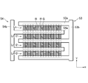
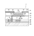
図10及び図11は表示装置1が備えるTFT基板2の一例を示す図である。図10Aは平面図である。図10Bは図10Aの拡大図である。図11は図10Bに示すXI-XI線で得られる断面図である。
図11に示すように、TFT基板2はガラスや樹脂などで形成される基板40を有している。表示装置1がトップエミッション型である場合には、基板40は透明でもよいし、不透明でもよい。表示装置1がボトムエミッション型である場合には、基板40は透明基板である。基板40上に選択トランジスタ10が形成される。一例では、基板40上に半導体層11が形成される。半導体層11は、例えば非晶質シリコンであるが、多結晶シリコンや、有機半導体、金属酸化物半導体などが半導体層11として用いられてもよい。基板40上にSiO2やSiNの下地層41が形成され、下地層41上に半導体層11が形成されてもよい。半導体層11は絶縁層42で覆われ、絶縁層42上にゲート電極14が形成される。走査線51は半導体層11と同じ導電層に形成されてもよい。ゲート電極14は層間絶縁層43で覆われ、層間絶縁層43上に第1ソース・ドレイン電極12と第2ソース・ドレイン電極13とが形成される。ソース・ドレイン電極12、13はスルーホールを介して半導体層11に接続される。ソース・ドレイン電極12、13はパッシベーション膜44によって覆われる。選択トランジスタ10の積層構造は図11に示すものに限られない。例えば、選択トランジスタ10はゲート電極14の上側に半導体層11が形成されてもよい。
パッシベーション膜44上に上述の絶縁層31が形成されている。絶縁層31は、例えば平坦化された表面を有する平坦化膜として機能する。平坦化膜は例えばアクリル樹脂で形成される。絶縁層31上に発光トランジスタ20が形成される。
一例では、図3A及び図3Bの例と同様に、絶縁層31上にゲート電極21が形成される。ゲート電極21はスルーホールを介して選択トランジスタ10の第2ソース・ドレイン電極13に接続される。スルーホールは絶縁層31とパッシベーション膜44とに形成される。ゲート電極21の上側に、量子ドットを含むチャネル層24が形成される。ゲート電極21は絶縁層32によって覆われ、絶縁層32上にチャネル層24が形成される。チャネル層24は、隣接する2つの画素の間で分離している。すなわち、一方の画素のチャネル層24と他方の画素のチャネル層24は接続していない。図11に示すように、ゲート電極21はチャネル層24よりも大きなサイズを有してもよい。すなわち、チャネル層24は、平面視において、ゲート電極21の外周縁の内側に存在してもよい。こうすることにより、チャネル層24に凹凸が生じることを抑えることができる。表示装置1は例えばトップエミッション型である。この場合、ゲート電極21は上述したように反射面を有する。ゲート電極21の全体が光を反射する材料で形成されてもよいし、ゲート電極21が複数の導電層によって構成され、その一部が光を反射する材料で形成されてもよい。
表示装置1は、上述したように、互いに異なる色で発光する複数の画素を有している。例えば、表示装置1は、図10A及び図10Bに示すように、赤画素(R)、緑画素(G)、及び青画素(B)の3つの画素を有する。量子ドットの発光波長(色)は、量子ドットのサイズに依存する。したがって、表示装置1の一例では、複数の画素のチャネル層24はサイズの異なる複数種類の量子ドットをそれぞれ含んでいる。すなわち、第1の色の画素(例えば、赤画素(R))のチャネル層24と、第2の色の画素(例えば、緑画素(G))のチャネル層24と、第3の色の画素(例えば、青画素(B))のチャネル層24は、互いにサイズが異なる3種類の量子ドットをそれぞれ含んでいる。
量子ドットのサイズは、色が異なる複数の画素において同じでもよい。例えば、第1の色の画素(例えば、赤画素(R))の量子ドットと、第2の色の画素(例えば、緑画素(G))の量子ドットと、第3の色の画素(例えば、青画素(B))の量子ドットは、同じサイズを有してもよい。この場合、カラーフィルター又は色変換フィルターを利用して、各画素の色を実現してもよい。カラーフィルターや色変換フィルターは、対向基板3に形成されてもよいし、TFT基板2に形成されてもよい。この場合、各画素のチャネル層24は、サイズの異なる複数種類の量子ドットを含んでもよい。例えば、チャネル層24は、サイズの異なる量子ドットでそれぞれ形成される複数の層を有してもよい。すなわち、チャネル層24は、第1のサイズを有する量子ドットの層と、第2のサイズを有する量子ドットの層と、第3のサイズを有する量子ドットの層を有してもよい。量子ドットの層の数は3つより多くてもよいし、3つより少なくてもよい。
チャネル層24上に第1電極22と第2電極23とが形成される。第1電極22はチャネル層24の一方の縁部に電気的に接続し、第2電極23はチャネル層24の反対側の縁部に電気的に接続している。第1電極22、第2電極23、及びチャネル層24は、図11に示すように、保護膜49によって覆われてもよい。そして、保護膜49の上側に対向基板3(図1)が配置されてもよい。
図11に示すように、絶縁層32上に、各画素に開口を有する絶縁層38が形成されてもよい。絶縁層38の開口の位置はゲート電極21の位置に対応している。チャネル層24は絶縁層38の開口の内側に形成され、絶縁層32を挟んでゲート電極21と対向している。絶縁層38の材料としては例えばアクリル樹脂が利用されてよい。第1電極22と第2電極23は絶縁層38上に形成さている。電極22、23の一部はチャネル層24上に位置し、チャネル層24に接続している。
TFT基板2には、上述したように、第1配線53と第2配線54とが形成される。一例では、図11に示すように、配線53、54は絶縁層38上に形成される。この場合、第1配線53の一部が第1電極22となり、第2配線54の一部が第2電極23となる。配線53、54が形成される層は、図11に示すものに限られない。後において説明するように、第1配線53と第2配線54はチャネル層24よりも下の層に形成されてもよい。
図10Bに示すように、互いに色が異なる複数の画素(図10A及び図10Bの例では、赤画素(R)、緑画素(G)、青画素(B))は、水平方向において規則的に並んでいる。各画素は矩形であり、垂直方向における画素の幅は、水平方向における画素の幅よりも大きい(図10A及び図10BではV方向が垂直方向であり、H方向が水平方向である)。チャネル層24も画素の形状に合わせて矩形である。第1電極22はチャネル層24の垂直方向における一方の縁部に接続し、第2電極23はチャネル層24の垂直方向における反対側の縁部に接続している。第1電極22と第2電極23が設けられる位置は図10A及び図10Bの例に限られない。例えば、第1電極22はチャネル層24の水平方向における一方の縁部に接続し、第2電極23はチャネル層24の水平方向における反対側の縁部に接続してもよい。すなわち、第1の方向におけるチャネル層24の幅が、第1の方向に直交する第2の方向における幅よりも大きい場合、第1電極22と第2電極23は第2の方向において互いに反対側に位置してもよい。
TFT基板2は複数の画素行Lを有している(図10A及び図10Bにおいては、各画素行Lに添字n~n+3が付されている)。複数の画素は各画素行Lにおいて一方向に並んでいる。各画素行Lは水平方向に並ぶ複数の画素によって構成されている。複数の画素行Lは垂直方向に並んでいる。図10A及び図10Bに示すように、色が異なる複数の画素(図10A及び図10Bの例では、赤画素(R))、緑画素(G)、及び青画素(B))が各画素行において規則的に並んでもよいし、図10A及び図10Bの例とは異なり、同じ色の画素が各画素行において並んでもよい。
第1配線53は、隣接する2つの画素行Lの間に形成され、水平方向に伸びている第1延伸部53aを含んでいる。そして、第1配線53の第1延伸部53aは、隣接する2つの画素行Lに含まれる複数の画素のチャネル層24に接続している。すなわち、第1配線53の第1延伸部53aは、隣接する2つの画素行Lに含まれる画素の第1電極22を構成している。第1配線53は複数の第1延伸部53aを含んでいる。また、第1配線53は、垂直方向に伸び且つ複数の第1延伸部53aを繋ぐ第2延伸部53bを含んでいる。
第1配線53と同様に、第2配線54も、隣接する2つの画素行Lの間に形成されている第1延伸部54aを含んでいる。そして、第2配線54の第1延伸部54aは、隣接する2つの画素行Lに含まれる画素のチャネル層24に接続している。すなわち、第2配線54の第1延伸部54aは、隣接する2つの画素行Lに含まれる複数の画素の第2電極23を構成している。第2配線54は複数の第1延伸部54aを含んでいる。また、第2配線54は、垂直方向に伸び且つ複数の第1延伸部54aを繋ぐ第2延伸部54bを含んでいる。第1配線53の第1延伸部53aと第2配線54の第1延伸部54aは垂直方向に交互に並んでいる。第1配線53の第2延伸部53bと第2配線54の第2延伸部54bは、水平方向に並ぶ複数の画素を挟んで互いに反対側に位置している。配線53、54のレイアウトは必ずしも図10A及び図10Bに示すものに限られない。垂直方向に並ぶ複数の第1延伸部53a、54aには一斉に電圧が加えられなくてもよい。例えば、複数の第1延伸部53a、54aには、画素行ごとに所定の方式で順番に電圧が加えられてよい。この場合、配線53、54のそれぞれは第2延伸部53b、54bを含んでいなくてもよい。
上述したように、各画素には保持容量26が形成されている。保持容量26は対向する2つの電極26a、26bを有している。第1電極26aは、図11に示すように、例えば選択トランジスタ10の半導体層11と同じ層に形成される。第2電極26bは、例えば絶縁層42上に形成される。第2電極26bは、ソース・ドレイン電極12、13と同様に、層間絶縁層42上に形成されてもよい。電極26a、26bのうち一方の電極は、選択トランジスタ10の第2ソース・ドレイン電極13に接続され、他方の電極は例えば第1配線53にスルーホールを介して接続される。
図12はTFT基板2の変形例を示す断面図である。この図では、これまで説明した箇所と同一箇所には同一符号を付している。この図に示すように、各画素の発光トランジスタ20は、チャネル層24を挟んでゲート電極21とは反対側に位置する補助電極25を有してもよい。この図の例では、チャネル層24上に絶縁層39が形成されている。そして、補助電極25は絶縁層39上に形成されている。補助電極25は例えばスルーホール(不図示)を介してゲート電極21に接続される。
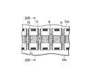
図13及び図14はTFT基板2のさらに別の変形例を示す断面図である。図13Aは平面図である。図13Bは図13Aの拡大図である。図14は図13Bに示すXIV-XIV線で得られる断面図である。この図では、これまで説明した箇所と同一箇所には同一符号を付している。
この図の例では、第1配線53と第2配線54はチャネル層24よりも下の層に形成されている。具体的には、第1配線53と第2配線54はパッシベーション膜44上に形成され、絶縁層31によって覆われている。第1電極22と第2電極23は、スルーホールを介して、第1配線53と第2配線54とにそれぞれ接続されている。第1配線53は、上述したように、隣接する2つの画素行Lの間に形成されている第1延伸部53aを有している。第1延伸部53aは絶縁層31、32、38に形成されているスルーホールを介して、第1電極22に接続されている。同様に、第2配線54は、隣接する2つの画素行Lの間に形成されている第1延伸部54aを有している。第1延伸部54aは絶縁層31、32、38に形成されているスルーホールを介して、第2電極23に接続されている。図13A、図13B、及び図14の例においても、補助電極25が、チャネル層24を挟んで、ゲート電極21とは反対側に位置する形成されてもよい。
図15はTFT基板2のさらに別の変形例を示す断面図である。この図では、これまで説明した箇所と同一箇所には同一符号を付している。
この図の例では、絶縁層31上に絶縁層38が形成されている。絶縁層38は、上述したように、各画素に開口を有している。ゲート電極21とチャネル層24は絶縁層38の開口の内側に形成されている。具体的には、ゲート電極21上に絶縁層32が形成され、絶縁層32上にチャネル層24が形成されている。絶縁層38は、開口の内周面に、傾斜面38aを有している。ゲート電極21の外周部21aは絶縁層38の傾斜面38a上に形成されている。このため、ゲート電極21の外周部21aは、各画素の中心に向かって斜め上方に傾斜している。また、この図の例では、ゲート電極21はチャネル層24からの光を反射する反射面を有している。ゲート電極21の外周部21aによると、チャネル層24から出て基板40に沿った方向に進む光がゲート電極21の外周部21aで反射され、表示装置1の表面から出る。図15の例では、各画素は、チャネル層24を挟んでゲート電極21とは反対側に位置する補助電極25を含んでいる。補助電極25は必ずしも形成されていなくてもよい。
発光トランジスタ20の積層構造は図11、図12、図14、及び図15に示すものに限られない。例えば、ゲート電極21、第1電極22、及び第2電極23は、チャネル層24に対して同じ側に形成されてもよい。例えば、図11、図12、及び図14に示す積層構造において、ゲート電極21は、チャネル層24の上側に形成されてもよい。この場合、ゲート電極21は絶縁層によって覆われ、この絶縁層の上側に第1電極22、及び第2電極23とが形成されてもよい。
Claims (11)
- 複数の画素と、
走査線と、
信号線と、
第1の配線と、
第2の配線と、を有し、
前記複数の画素のうち少なくとも1つの画素は、
前記走査線に接続されているゲート電極と、前記信号線に接続されている第1のソース・ドレイン電極と、第2のソース・ドレイン電極とを有している選択トランジスタと、
前記選択トランジスタの前記第2のソース・ドレイン電極を通して前記少なくとも1つの画素の階調値に応じた電圧が加えられるゲート電極と、前記第1の配線に接続されている第1の電極と、前記第2の配線に接続されている第2の電極と、量子ドットを含んでいるチャネル層とを有し、前記チャネル層を流れるキャリアにより前記量子ドットを発光させる発光トランジスタと、
を有している表示装置。 - 前記発光トランジスタの前記チャネル層は前記発光トランジスタの前記ゲート電極の上側に形成され、
前記発光トランジスタの前記第1の電極と前記第2の電極は前記チャネル層の上側に形成されている
請求項1に記載の表示装置。 - 前記発光トランジスタの前記ゲート電極は、前記量子ドットからの光を反射する反射面を有している
請求項2に記載の表示装置。 - 前記発光トランジスタの前記ゲート電極と前記第1の電極と前記第2の電極は、前記チャネル層の上側に形成されている
請求項1に記載の表示装置。 - 前記複数の画素のそれぞれに開口を有している絶縁層をさらに備え
前記発光トランジスタの前記チャネル層は前記絶縁層の前記開口の内側に配置され、
前記発光トランジスタの前記第1の電極と前記第2の電極は前記チャネル層と前記絶縁層の上側に形成されている
請求項1に記載の表示装置。 - 前記絶縁層の前記開口は、その内周面に、傾斜面を有し、
前記発光トランジスタの前記チャネル層と前記発光トランジスタの前記ゲート電極は前記絶縁層の前記開口の内側に形成され、
前記発光トランジスタの前記ゲート電極の外周部は前記絶縁層の前記開口の傾斜面に形成されている
請求項5に記載の表示装置。 - 前記発光トランジスタは、前記チャネル層を挟んで前記ゲート電極とは反対側に形成されている補助電極を有している
請求項1に記載の表示装置。 - 前記複数の画素は、前記少なくとも1つの画素として、第1の画素と前記第1の画素に隣接する第2の画素とを含み、
前記第1の画素の量子ドットのサイズと、前記第2の画素の量子ドットのサイズは互いに異なっている
請求項1に記載の表示装置。 - 前記複数の画素は、前記少なくとも1つの画素として、第1の画素と第2の画素と第3の画素と第4の画素とを有し、
前記第1の画素と前記第2の画素は第1の行を構成し、
前記第3の画素と前記第4の画素は第2の行を構成し、
前記第1の配線と前記第2の配線のうちの一方の配線は、前記第1の行と前記第2の行との間に位置し、前記第1の画素と前記第2の画素と第3の画素と第4の画素の前記チャネル層に接続している
請求項1に記載の表示装置。 - 前記第1の配線と前記第2の配線は交互に並んでいる
請求項9に記載の表示装置。 - 前記発光トランジスタの前記チャネル層は、前記第1の電極に接触している第1の領域と、前記第2の電極に接触している第2の領域と、前記第1の領域と前記第2の領域との間の領域である第3の領域とを有し、
前記第1の領域と前記第2の領域のうち少なくとも一方の領域には、不純物が添加されている
請求項1に記載の表示装置。
Priority Applications (1)
| Application Number | Priority Date | Filing Date | Title |
|---|---|---|---|
| US15/661,514 US10243032B2 (en) | 2015-01-28 | 2017-07-27 | Display device |
Applications Claiming Priority (2)
| Application Number | Priority Date | Filing Date | Title |
|---|---|---|---|
| JP2015014573A JP2016139560A (ja) | 2015-01-28 | 2015-01-28 | 表示装置 |
| JP2015-014573 | 2015-01-28 |
Related Child Applications (1)
| Application Number | Title | Priority Date | Filing Date |
|---|---|---|---|
| US15/661,514 Continuation US10243032B2 (en) | 2015-01-28 | 2017-07-27 | Display device |
Publications (1)
| Publication Number | Publication Date |
|---|---|
| WO2016121698A1 true WO2016121698A1 (ja) | 2016-08-04 |
Family
ID=56543311
Family Applications (1)
| Application Number | Title | Priority Date | Filing Date |
|---|---|---|---|
| PCT/JP2016/052029 Ceased WO2016121698A1 (ja) | 2015-01-28 | 2016-01-25 | 表示装置 |
Country Status (3)
| Country | Link |
|---|---|
| US (1) | US10243032B2 (ja) |
| JP (1) | JP2016139560A (ja) |
| WO (1) | WO2016121698A1 (ja) |
Cited By (3)
| Publication number | Priority date | Publication date | Assignee | Title |
|---|---|---|---|---|
| US12211883B2 (en) | 2019-07-30 | 2025-01-28 | Nichia Corporation | Method for manufacturing image display device and image display device |
| US12543419B2 (en) | 2019-10-01 | 2026-02-03 | Nichia Corporation | Image display device manufacturing method including providing substrate including circuit and insulating film, forming conductive layer on insulating film, and forming semiconductor layer on conductive layer |
| JP2026028202A (ja) * | 2024-08-06 | 2026-02-19 | ポステック・リサーチ・アンド・ビジネス・ディベロップメント・ファウンデーション | 低周波ノイズが除去された素子 |
Families Citing this family (4)
| Publication number | Priority date | Publication date | Assignee | Title |
|---|---|---|---|---|
| JP7432845B2 (ja) | 2019-05-10 | 2024-02-19 | 日亜化学工業株式会社 | 画像表示装置の製造方法および画像表示装置 |
| KR102459943B1 (ko) * | 2019-12-19 | 2022-10-26 | 한양대학교 산학협력단 | 단백질을 포함하는 나노복합체 기반의 전자 시냅스 소자 및 이의 제조 방법 |
| JP2021157934A (ja) * | 2020-03-26 | 2021-10-07 | 株式会社ジャパンディスプレイ | 表示装置及び表示装置 |
| WO2022079817A1 (ja) * | 2020-10-14 | 2022-04-21 | シャープ株式会社 | 発光素子 |
Citations (5)
| Publication number | Priority date | Publication date | Assignee | Title |
|---|---|---|---|---|
| JPH09260611A (ja) * | 1996-03-19 | 1997-10-03 | Toshiba Corp | 電子デバイス |
| JP2008053293A (ja) * | 2006-08-22 | 2008-03-06 | Sony Corp | 電子デバイス及びその製造方法 |
| JP2009206505A (ja) * | 2008-01-29 | 2009-09-10 | Semiconductor Energy Lab Co Ltd | 発光装置 |
| US20120280208A1 (en) * | 2011-05-06 | 2012-11-08 | Faquir Chand Jain | Quantum dot channel (qdc) quantum dot gate transistors, memories and other devices |
| JP2014078381A (ja) * | 2012-10-10 | 2014-05-01 | Konica Minolta Inc | 白色エレクトロルミネッセンスデバイス及び白色エレクトロルミネッセンスデバイスの製造方法 |
Family Cites Families (2)
| Publication number | Priority date | Publication date | Assignee | Title |
|---|---|---|---|---|
| US7888700B2 (en) | 2007-03-08 | 2011-02-15 | Eastman Kodak Company | Quantum dot light emitting device |
| JP5572968B2 (ja) | 2009-03-06 | 2014-08-20 | 大日本印刷株式会社 | 量子ドット発光材料、及び発光デバイス |
-
2015
- 2015-01-28 JP JP2015014573A patent/JP2016139560A/ja active Pending
-
2016
- 2016-01-25 WO PCT/JP2016/052029 patent/WO2016121698A1/ja not_active Ceased
-
2017
- 2017-07-27 US US15/661,514 patent/US10243032B2/en active Active
Patent Citations (5)
| Publication number | Priority date | Publication date | Assignee | Title |
|---|---|---|---|---|
| JPH09260611A (ja) * | 1996-03-19 | 1997-10-03 | Toshiba Corp | 電子デバイス |
| JP2008053293A (ja) * | 2006-08-22 | 2008-03-06 | Sony Corp | 電子デバイス及びその製造方法 |
| JP2009206505A (ja) * | 2008-01-29 | 2009-09-10 | Semiconductor Energy Lab Co Ltd | 発光装置 |
| US20120280208A1 (en) * | 2011-05-06 | 2012-11-08 | Faquir Chand Jain | Quantum dot channel (qdc) quantum dot gate transistors, memories and other devices |
| JP2014078381A (ja) * | 2012-10-10 | 2014-05-01 | Konica Minolta Inc | 白色エレクトロルミネッセンスデバイス及び白色エレクトロルミネッセンスデバイスの製造方法 |
Cited By (3)
| Publication number | Priority date | Publication date | Assignee | Title |
|---|---|---|---|---|
| US12211883B2 (en) | 2019-07-30 | 2025-01-28 | Nichia Corporation | Method for manufacturing image display device and image display device |
| US12543419B2 (en) | 2019-10-01 | 2026-02-03 | Nichia Corporation | Image display device manufacturing method including providing substrate including circuit and insulating film, forming conductive layer on insulating film, and forming semiconductor layer on conductive layer |
| JP2026028202A (ja) * | 2024-08-06 | 2026-02-19 | ポステック・リサーチ・アンド・ビジネス・ディベロップメント・ファウンデーション | 低周波ノイズが除去された素子 |
Also Published As
| Publication number | Publication date |
|---|---|
| US20180012951A1 (en) | 2018-01-11 |
| JP2016139560A (ja) | 2016-08-04 |
| US10243032B2 (en) | 2019-03-26 |
Similar Documents
| Publication | Publication Date | Title |
|---|---|---|
| US10243032B2 (en) | Display device | |
| TWI702455B (zh) | 電致發光顯示裝置 | |
| US12232390B2 (en) | Display apparatus with organic light-emitting diodes | |
| CN114391187B (zh) | 场致发光元件以及场致发光装置 | |
| JP7465074B2 (ja) | ディスプレイ装置 | |
| JP7190740B2 (ja) | エレクトロルミネセンス素子を有する表示装置 | |
| CN109698259B (zh) | 应用各向异性纳米棒的发光二极管及包括其的发光装置 | |
| US7456431B2 (en) | Organic light emitting display | |
| KR20190029470A (ko) | 양자점 발광다이오드 및 이를 포함하는 양자점 발광표시장치 | |
| KR20190029353A (ko) | 유기 발광 소자 및 이를 포함하는 유기 발광 표시 장치 | |
| CN108023024A (zh) | 量子点发光二极管和包括其的量子点显示装置 | |
| CN112369123B (zh) | 光电子元件、使用该元件的平面显示器及光电子元件的制造方法 | |
| US20230255039A1 (en) | Light-emitting device | |
| US10205113B2 (en) | Organic electroluminescence device including an emissive layer including an assistant dopant layer and light-emitting dopant layer | |
| KR101182268B1 (ko) | 유기 발광 장치 | |
| US9692002B2 (en) | Organic light emitting display device | |
| KR102672009B1 (ko) | 유기 발광 소자 및 이를 포함하는 유기 발광 표시 장치 | |
| KR20220155794A (ko) | 표시 장치 | |
| CN113545168A (zh) | 发光元件及使用了该发光元件的显示装置 | |
| US20120007501A1 (en) | Display device | |
| US20250107314A1 (en) | Display device and method for manufacturing the same | |
| JP5536349B2 (ja) | 画像表示装置 | |
| KR20240006102A (ko) | 표시 장치 및 이의 제조 방법 | |
| KR20230173263A (ko) | 표시 장치 및 이의 제조 방법 | |
| KR20230173259A (ko) | 표시 장치 및 이의 제조 방법 |
Legal Events
| Date | Code | Title | Description |
|---|---|---|---|
| 121 | Ep: the epo has been informed by wipo that ep was designated in this application |
Ref document number: 16743301 Country of ref document: EP Kind code of ref document: A1 |
|
| NENP | Non-entry into the national phase |
Ref country code: DE |
|
| 122 | Ep: pct application non-entry in european phase |
Ref document number: 16743301 Country of ref document: EP Kind code of ref document: A1 |