WO2016121131A1 - High-frequency-isolation gate driver circuit and gate circuit driving method - Google Patents
High-frequency-isolation gate driver circuit and gate circuit driving method Download PDFInfo
- Publication number
- WO2016121131A1 WO2016121131A1 PCT/JP2015/054726 JP2015054726W WO2016121131A1 WO 2016121131 A1 WO2016121131 A1 WO 2016121131A1 JP 2015054726 W JP2015054726 W JP 2015054726W WO 2016121131 A1 WO2016121131 A1 WO 2016121131A1
- Authority
- WO
- WIPO (PCT)
- Prior art keywords
- circuit
- gate driver
- voltage
- gate
- current
- Prior art date
Links
- 238000002955 isolation Methods 0.000 title claims abstract description 30
- 238000000034 method Methods 0.000 title claims description 19
- 230000005284 excitation Effects 0.000 claims abstract description 52
- 238000009413 insulation Methods 0.000 claims description 54
- 238000006243 chemical reaction Methods 0.000 claims description 51
- 230000000295 complement effect Effects 0.000 claims description 32
- 238000004804 winding Methods 0.000 claims description 13
- 230000005540 biological transmission Effects 0.000 claims description 8
- 230000015572 biosynthetic process Effects 0.000 claims description 4
- 239000003990 capacitor Substances 0.000 claims description 4
- 230000005415 magnetization Effects 0.000 description 20
- 230000007257 malfunction Effects 0.000 description 5
- 230000003071 parasitic effect Effects 0.000 description 5
- 238000010586 diagram Methods 0.000 description 3
- 238000006073 displacement reaction Methods 0.000 description 3
- 230000000694 effects Effects 0.000 description 3
- 230000004907 flux Effects 0.000 description 3
- 230000000630 rising effect Effects 0.000 description 3
- 230000003321 amplification Effects 0.000 description 2
- 239000000470 constituent Substances 0.000 description 2
- 230000007423 decrease Effects 0.000 description 2
- 230000004048 modification Effects 0.000 description 2
- 238000012986 modification Methods 0.000 description 2
- 238000003199 nucleic acid amplification method Methods 0.000 description 2
- 239000004020 conductor Substances 0.000 description 1
- 230000003111 delayed effect Effects 0.000 description 1
- ORQBXQOJMQIAOY-UHFFFAOYSA-N nobelium Chemical compound [No] ORQBXQOJMQIAOY-UHFFFAOYSA-N 0.000 description 1
- 239000004065 semiconductor Substances 0.000 description 1
- 230000002269 spontaneous effect Effects 0.000 description 1
Images


Classifications
-
- H—ELECTRICITY
- H02—GENERATION; CONVERSION OR DISTRIBUTION OF ELECTRIC POWER
- H02M—APPARATUS FOR CONVERSION BETWEEN AC AND AC, BETWEEN AC AND DC, OR BETWEEN DC AND DC, AND FOR USE WITH MAINS OR SIMILAR POWER SUPPLY SYSTEMS; CONVERSION OF DC OR AC INPUT POWER INTO SURGE OUTPUT POWER; CONTROL OR REGULATION THEREOF
- H02M1/00—Details of apparatus for conversion
- H02M1/08—Circuits specially adapted for the generation of control voltages for semiconductor devices incorporated in static converters
-
- H—ELECTRICITY
- H03—ELECTRONIC CIRCUITRY
- H03K—PULSE TECHNIQUE
- H03K17/00—Electronic switching or gating, i.e. not by contact-making and –breaking
- H03K17/16—Modifications for eliminating interference voltages or currents
- H03K17/161—Modifications for eliminating interference voltages or currents in field-effect transistor switches
- H03K17/162—Modifications for eliminating interference voltages or currents in field-effect transistor switches without feedback from the output circuit to the control circuit
-
- H—ELECTRICITY
- H03—ELECTRONIC CIRCUITRY
- H03K—PULSE TECHNIQUE
- H03K17/00—Electronic switching or gating, i.e. not by contact-making and –breaking
- H03K17/51—Electronic switching or gating, i.e. not by contact-making and –breaking characterised by the components used
- H03K17/56—Electronic switching or gating, i.e. not by contact-making and –breaking characterised by the components used by the use, as active elements, of semiconductor devices
- H03K17/567—Circuits characterised by the use of more than one type of semiconductor device, e.g. BIMOS, composite devices such as IGBT
-
- H—ELECTRICITY
- H03—ELECTRONIC CIRCUITRY
- H03K—PULSE TECHNIQUE
- H03K17/00—Electronic switching or gating, i.e. not by contact-making and –breaking
- H03K17/51—Electronic switching or gating, i.e. not by contact-making and –breaking characterised by the components used
- H03K17/56—Electronic switching or gating, i.e. not by contact-making and –breaking characterised by the components used by the use, as active elements, of semiconductor devices
- H03K17/687—Electronic switching or gating, i.e. not by contact-making and –breaking characterised by the components used by the use, as active elements, of semiconductor devices the devices being field-effect transistors
- H03K17/6871—Electronic switching or gating, i.e. not by contact-making and –breaking characterised by the components used by the use, as active elements, of semiconductor devices the devices being field-effect transistors the output circuit comprising more than one controlled field-effect transistor
-
- H—ELECTRICITY
- H03—ELECTRONIC CIRCUITRY
- H03K—PULSE TECHNIQUE
- H03K7/00—Modulating pulses with a continuously-variable modulating signal
- H03K7/08—Duration or width modulation ; Duty cycle modulation
Definitions
- the present invention relates to a gate driver circuit for driving a gate circuit of a semiconductor switching element and a method for driving the gate circuit, and is applied to a high frequency amplification apparatus for outputting high frequency power of 1 MHz to 100 MHz.
- a gate circuit of a switching element for driving a load is connected in series with a main power supply, and the current direction of the load is switched by a bridge circuit or the like.
- FIG. 9A shows a configuration example of the power conversion device.
- a full bridge is configured by the switching elements 101A to 101D and the connection between the drive power supply 103 and the load 104 is switched is shown.
- the switching elements 101A to 101D are controlled on / off by the gate driver circuits 102A to 102D, respectively.
- the gate driver circuit 102A and the gate driver circuit 102C control ON / OFF of the switching element 101A and the switching element 101C by the high-voltage side input signals SA and SC, and the gate driver circuit 102B and the gate driver circuit 102D are on the low voltage side.
- the on / off control of the switching element 101B and the switching element 101D is controlled by the input signals S-B and S-D of FIG.
- FIG. 9B shows a configuration example of a power conversion device using an insulation element.
- a half bridge is configured by the switching elements 101A and 101B and the connection between the drive power supply 103 and the load 104 is switched is shown.
- the insulating elements 105A and 105B are connected to the input side of the gate driver circuits 102A and 102B, and the input signals S-A and S-B are electrically isolated from the insulating drive signal Siso by the insulating elements 105A and 105B.
- a photocoupler and a pulse transformer are known as an insulating element which electrically isolates an input signal of a gate driver circuit. (Patent publication 1, 2)
- the pulse transformer is used as a transformer for driving a gate circuit and is also called a gate driver transformer.
- FIG. 10 shows an example of a circuit using a photocoupler.
- the drive circuit shown in FIG. 10A by connecting the photocouplers 105A and 105B to the gate driver circuits 102A and 102B for driving the switching elements 101A and 101B, an input signal SA and an insulation drive signal Siso-A and And the isolation between the input signal SB and the isolation drive signal Siso-B.
- a driver built-in RF-MOS module can be configured by combining a switching element 101 such as a high frequency MOS-FET and a gate driver circuit 102 such as an FET driver.
- FIG. 10 shows drive signal waveforms.
- B-1) shows an input signal SA on the high voltage side
- (b-3) shows an insulation drive signal Siso-A on the high voltage side obtained by insulation with a photocoupler.
- (b-2) shows the low-voltage side input signal S-B
- (b-4) shows the low-voltage side insulation drive signal Siso-B obtained by insulation with a photocoupler.
- FIG. 11 shows an example of a circuit that performs insulation using a gate driver transformer (pulse transformer).
- a gate driver transformer pulse transformer
- FIG. 11A by connecting free magnetization transformer circuits 106A and 106B to gate driver circuits 102A and 102B for driving switching elements 101A and 101B, an input signal SA and an insulation drive signal Siso- The insulation with A and the insulation between the input signal S-B and the insulation drive signal Siso-B are performed.
- the switching elements 101A and 101B such as high frequency MOS-FETs and the gate driver circuits 102A and 120B such as FET drivers are combined.
- a driver built-in RF-MOS module can be configured.
- Free magnetization transformer circuits 106A and 106B shown in FIG. 11 are insulating circuits in which gate driver transformers (pulse transformers) are configured in a forward system, and FET 106b is connected in series to the primary side coil of gate driver transformers (pulse transformers) 106a.
- a series circuit of a rectifying diode and a resistor is connected in parallel to the primary side coil, and a rectifying circuit 106d is connected to the output end on the secondary coil side.
- the transformer In the free magnetization transformer circuit 106, the transformer is excited in only one direction, and the magnetization state is reset by releasing energy stored in the coil while the switching element is in the off state.
- a series circuit of a rectifier diode and a resistor connected in parallel to the primary coil constitutes a reset circuit (snubber circuit) 106c.
- FIG. 11 shows drive signal waveforms.
- (B-1) shows the input signal S-A on the high voltage side
- (b-2) shows the input signal S-B on the low voltage side
- (b-3) shows the high voltage obtained by insulation with the gate driver transformer
- the isolation drive signal Siso-A on the side is shown
- (b-4) shows the isolation drive signal Siso-B on the low voltage side obtained by isolation with the gate driver transformer.
- the circuit configuration using a photocoupler as the insulating element has the following problems. (1) When a photocoupler is used, there is a problem that a phase difference occurs in the signal before and after the insulation.
- the isolation drive signal Siso-A has a phase difference with respect to the input signal SA before isolation.
- the insulation drive signal after insulation due to the variation of the threshold inside the photocoupler The pulse width of Siso-B increases or decreases as compared to the input signal S-B before isolation.
- the dead time between the high voltage side isolation drive signal Siso-A and the low voltage side isolation drive signal Siso-B becomes short like Td-2, and the switching element 101A And a short circuit occurs between the RF-MOS FETs of the switching element 101B.
- FIG. 11 (c) shows the drive signal waveform after insulation.
- an excitation current flowing in a primary coil of the gate driver transformer is always flowed without alternately interrupting in both directions. This eliminates the need for a reset period caused by the excitation current flowing only in one direction, and eliminates the occurrence of the self-resonance phenomenon after the reset. By not generating the self-resonance phenomenon, it is possible to suppress the generation of the noise current due to the self-resonance phenomenon and to suppress the malfunction of the switching element due to the noise.
- the present invention can be an aspect of an apparatus and an aspect of a method. The following description will be made based on the reference numerals shown in FIGS. 1 to 3.
- the high frequency insulated gate driver circuit of the present invention drives multiple gate circuits with high frequency signals isolated from one another.
- the high frequency insulated gate driver circuit includes an input signal forming circuit, a gate driver transformer, and a current-voltage conversion circuit.
- the input signal forming circuit outputs two input signals (S) of complementary voltage signals which are out of phase with each other at the same duty ratio.
- the two input signals have complementary potential periods in which the voltages of the respective phases are in a complementary relationship between the high potential and the low potential, and the same potential periods in which the voltages of the respective phases are the same.
- Each potential of the two input signals alternates between high and low potentials in time series.
- One form of the input signal forming circuit outputs a high potential or low potential input signal (S) based on a pulse signal forming circuit (11) forming a high frequency pulse signal (PS) and a binary value of the high frequency pulse signal And two gate driver transformer drive elements (12).
- Another form of the input forming signal circuit comprises a control circuit (13) for forming a high frequency pulse signal, and based on a binary signal of the high frequency pulse signal formed by the control circuit (13), a high potential or low potential input It comprises two gate driver transformer drive elements (12) for outputting a signal (S).
- the high side gate driver transformer drive element forms a high potential input signal based on the power supply voltage
- the low side gate driver transformer drive element is the ground voltage or zero.
- a low potential input signal is formed based on a reference voltage including a voltage.
- a voltage obtained by subtracting the voltage drop is formed as an input signal.
- the high side gate driver transformer drive element forms a high potential input signal based on a positive power supply voltage
- the low side gate driver transformer drive element Forms a low potential input signal based on the negative power supply voltage
- Gate driver transformer In the gate driver transformer (20), the output terminal of each phase of the input signal forming circuit is connected to each input terminal at both ends of the primary side coil.
- the gate driver transformer receives an input signal (S) and forms a signal isolated from the input signal.
- the gate driver transformer included in the present invention has two input signals (S) applied to both ends of the primary side coil, as well as complementary potential periods in which the voltages of the phases are complementary between high and low potentials. It has the same potential period in which the voltages of the phases have the same potential.
- An excitation current (im) and a load current (iL) flow in the complementary potential period in the primary side coil of the gate driver transformer (20), and an excitation current (im) flows in the same potential period.
- the excitation current (im) always flows through the primary coil for the entire period.
- the reset period for resetting the excitation current can be eliminated. it can.
- the generation of the noise current due to the self-resonance phenomenon can be suppressed by the excitation current flowing through the primary side coil in the same potential period.
- the excitation current (im) always flows through the primary coil for the entire period, so the coil is always kept magnetized.
- a free magnetization transformer used in a conventional insulating circuit there is a period in which no excitation current flows after the excitation current is reset, and in this period, the flux state of the coil is in a free state not controlled by the gate driver transformer circuit. In a period, a noise current may occur due to a self-resonance phenomenon.
- the gate driver transformer included in the present invention is referred to as a constrained magnetization transformer with respect to a conventional free magnetization transformer.
- the output terminal of the gate driver transformer (20) is connected to the input terminal, and the secondary current flowing to the secondary side coil of the gate driver transformer is current-voltage converted to obtain the isolated The drive signal (Siso) is output to the gate circuit.
- the current-voltage conversion circuit (30) of the present invention can be configured by connecting in parallel a first parallel circuit formed by connecting a resistor and a rectifying diode in parallel and a second parallel circuit.
- the rectifying diodes are connected in series such that the forward direction is in the direction of the gate circuit on the winding start side of the secondary coil of the gate driver transformer.
- the rectifying diodes are connected in parallel between the winding start side and the winding end side of the secondary coil of the gate driver transformer so that the forward direction is in the direction of the input end of the gate circuit.
- the current-to-voltage conversion circuit of the present invention uses the resistor connected in series in the first parallel circuit and the resistor connected in parallel in the second parallel circuit to convert the current flowing in the secondary coil of the gate driver transformer into a voltage -It is possible to rectify in the current direction toward the gate driver circuit side by voltage conversion and the rectifying action of a rectifying diode connected in parallel to each resistor.
- the first parallel circuit and / or the second parallel circuit may be configured to connect capacitors in parallel.
- the current-voltage conversion circuit of the present invention can be in a plurality of forms.
- the input impedance viewed from the gate driver transformer is adjusted to a predetermined value by the resistance value of the resistance of the first parallel circuit and the resistance value of the resistance of the second parallel circuit.
- the resistance value of the resistance of the first parallel circuit and the resistance value of the resistance of the second parallel circuit equal, the impedance seen from the gate driver transformer on the output side can always be made constant.
- the equivalent resistance value is not limited to the same resistance value but includes an allowance.
- the resistance value of the resistance of the first parallel circuit and the resistance value of the resistance of the second parallel circuit are transmitted between the gate driver transformer and the current-voltage conversion circuit. It is selected to be the same as the characteristic impedance of. According to the second aspect, the input signal input to the primary side of the gate driver transformer can be transmitted to the gate driver circuit as an isolation drive signal without distortion.
- a common mode transformer is provided on the primary side or the secondary side of the gate driver transformer, and the characteristic impedance of the common mode transformer is set between the gate driver transformer and the current-voltage conversion circuit. Match the characteristic impedance of the transmission line.
- the common mode transformer prevents the common mode noise current flowing in the same direction through the parasitic capacitance between the primary coil and the secondary coil of the gate driver transformer, thereby reducing the influence of the displacement voltage. It can be done.
- the gate circuit of this invention can comprise a high frequency switching module with a switching element and the gate driver circuit which drives a switching element.
- the gate driver circuit performs on / off control of the switching element by the isolation drive signal (Siso) output from the current-voltage conversion circuit.
- isolation drive signal Siso
- high frequency switching modules may be controlled as a unit.
- the high frequency insulated gate driver circuit of the present invention can be configured as a full bridge or a half bridge.
- the unit which comprises a bridge can be made into a high frequency switching module other than a gate circuit.
- a high frequency insulated gate driver circuit is connected to each of the high voltage gate circuit applying high voltage to the load and the input terminal of the low voltage gate circuit applying low voltage to the load.
- the gate circuit driving method of the present invention is a method of driving a plurality of gate circuits by a plurality of high frequency signals insulated from each other, and the same duty ratio is applied to each input terminal at both ends of the primary side coil of the gate driver transformer (20). And complementary voltage periods in which the voltages of the respective phases are complementary between the high voltage and the low voltage, and the same voltage periods in which the voltages of the respective phases are the same voltage.
- the two input signals (S) comprising switching each potential alternately in high and low potentials in time series are applied, and in the primary side coil of the gate driver transformer (20), excitation current and load are applied in complementary potential periods.
- An isolation drive signal obtained by current-voltage conversion of the secondary current flowing in the secondary side coil of the gate driver transformer (20) by flowing current and flowing excitation current in the same potential period. Enter the iso) to the gate circuit, to drive the gate circuit by an insulating drive signal (Siso).
- the two input signals (S) applied to both ends of the primary side coil have complementary potential periods in which the voltages of the phases are complementary to each other.
- Excitation current (im) and load current (iL) are supplied to the primary side coil of the gate driver transformer (20) in the complementary electric potential period with the same electric potential period in which the voltages of the respective phases are the same electric potential. Pass an exciting current (im). Due to the flow of the excitation current, the excitation current (im) flows through the primary coil for the entire period.
- the reset period for resetting the excitation current can be eliminated. it can.
- the generation of the noise current due to the self-resonance phenomenon can be suppressed by the excitation current flowing through the primary side coil in the same potential period.
- current-voltage conversion is performed by the current-voltage conversion circuit (30) connected to the secondary coil of the gate driver transformer (20).
- the current-voltage conversion circuit is configured by connecting in parallel a first parallel circuit formed by connecting a resistor and a rectification diode in parallel and a second parallel circuit, and the winding of the secondary side coil of the gate driver transformer
- a parallel circuit of a resistor and a rectifier diode wherein the first parallel circuit is connected in series with the forward direction of the rectifier diode directed to the gate circuit, and the winding of the secondary coil of the gate driver transformer
- the potential of the isolation drive signal (Siso) is forward directed by the rectifier diode of the second parallel circuit. Reverse bias by voltage.
- the differential voltage of the input signal (S) is a negative voltage with respect to the forward direction of the rectifier diode of the first parallel circuit
- the input side of the first parallel circuit has a low potential
- the second parallel circuit The output side of the connected first parallel circuit is at a high potential, which corresponds to a negative voltage period in which a negative voltage is applied to the current-voltage conversion circuit.
- generation of two input signals can be performed using two gate driver transformer driving elements, and one of the gate driver transformer driving elements is a binary high frequency pulse signal (PS).
- a high potential signal is applied to generate a high potential input signal (S)
- a low potential signal of a binary high frequency pulse signal (PS) is applied to the other gate driver transformer drive element to generate a low potential.
- S Generate an input signal
- An isolation drive signal (Siso) obtained from the input signal (S) by the insulating function of the gate driver transformer and current-voltage conversion is input to the gate driver circuit, and the drive voltage is generated by the gate driver circuit, and the generated drive voltage Control the on / off of the switching element of the gate circuit.
- the duty of the isolated drive signal can be adjusted by changing the phase difference between the two input signals (S). This duty adjustment can be performed while maintaining the impedance at low impedance for the entire period.
- the reset period of the excitation current can be made unnecessary, and the occurrence of the self-resonance phenomenon after the reset can be prevented.
- the generation of noise due to the self-resonance phenomenon can be suppressed by constantly flowing the excitation current, and the malfunction of the switching element can be suppressed.
- the high frequency insulated gate driver circuit and the gate circuit driving method according to the present invention are suitable for high frequencies in the 1 MHz to 100 MHz band that are difficult to cope with photocouplers and free magnetization transformers, and high frequency amplification that outputs high frequency power from 1 MHz to 100 MHz. It can be adapted to the device.
- FIG. 7 is a diagram for explaining the reverse bias effect of the current-voltage conversion circuit, and the pulse width adjustment of the isolated drive signal. It is a figure for demonstrating the other structural example of the high frequency insulation gate driver circuit of this invention.
- FIG. 1 the schematic configuration of the high frequency insulated gate driver circuit of the present invention will be described with reference to FIG. 1, and one structural example and operation example of the high frequency insulated gate driver circuit of the present invention will be described with reference to FIGS.
- FIG. 8 Another structural example of the high frequency insulated gate driver circuit of the present invention will be described using FIG. 8, and a structural example of a gate driver transformer drive element included in the high frequency insulated gate driver circuit of the present invention will be described using FIG.
- FIG. 1 is a view for explaining a schematic configuration of a high frequency insulated gate driver circuit of the present invention
- FIG. 1 (a) shows a configuration for generating a pulse signal for forming an input signal in an input signal forming circuit.
- FIG. 1 (b) shows a configuration in which a pulse signal for forming an input signal is introduced from outside the input signal forming circuit.
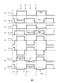
- FIG. 1 shows a configuration example of a half bridge circuit having two switching elements
- the present invention can also be applied to a configuration example of a full bridge circuit having four switching elements.
- the switching circuit in the half bridge configuration connects the switching elements 50A and 50B in series to form a series circuit, and connects the load power supply 70 to both ends of the series circuit.
- a series circuit of two capacitors is connected in parallel to the series circuit of switching elements, and a load 60 is connected between the middle point of the series circuit of switching elements and the middle point of the series circuit of capacitors.
- the switching element 50 (50A, 50B) and the gate driver circuit 40 (40A, 40B) can be configured as one circuit as the high frequency switching module 2 (2A, 2B).
- FIG. 1 shows an example in which the high frequency switching module 2 is configured by a half bridge, it may be configured by a full bridge.
- the high frequency insulated gate driver circuit 1 (1A, 1B) is connected to the gate driver circuit 40 (40A, 40B) or the high frequency switching module 2 (2A, 2B).
- the high frequency insulated gate driver circuit 1 (1A, 1B) inputs the insulated drive signal (Siso (Siso-A, Siso-B)) to the gate driver circuit 40 (40A, 40B), and switches the switching element 50 (50A, 50B). ) Control on / off.
- the input signal formation circuit 10, the gate driver transformer 20, the current-voltage conversion circuit 30, and the gate driver circuit 40 constitute a switching element drive circuit 3 (3A, 3B).
- the on / off control of the switching element 50 switches the connection state between the load power supply 70 and the load 60, and switches the voltage state applied to the load 60.
- the high frequency switching module 2A applies a high voltage to the load 60
- the high frequency switching module 2B applies a low voltage to the load 60.
- the high frequency insulation gate driver circuit 1A inputs the insulation drive signal (Siso-A) to the high frequency side high frequency switching module 2A, and the high frequency insulation gate driver circuit 1B inputs the insulation drive signal (Siso-B) to the low frequency side high frequency switching module 2B. Enter
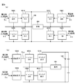
- Each high frequency insulated gate driver circuit 1 (1A, 1B) includes a gate driver transformer drive element 12 (12A, 12B), a gate driver transformer 20 (20A, 20B), and a current-voltage conversion circuit 30 (30A, 30B). .
- the gate driver transformer drive element 12 (12A, 12B) generates two input signals (S-1, S-2) based on the two pulse signals (PS-1, PS-2).
- the two generated input signals (S-1, S-2) are applied to the gate driver transformer 20 (20A, 20B).
- the input signal (S) is complementary voltage signals having the same duty ratio and phase-shifted to each other, and complementary voltage periods in which the voltages of the phases are complementary to each other, and the voltages of the phases Are alternately switched between the high potential and the low potential in time series.
- the input signal (S) comprises an input signal (S-1) and an input signal (S-2) of two voltage signals of different potentials, and the input signal (S) is input to each end of the primary side coil of the gate driver transformer 20 Be done.
- the gate driver transformer 20 (20A, 20B) is an insulating element for insulating the input signal (S) and the insulation drive signal (Siso), and is constituted by a high frequency transformer also called a pulse transformer.
- the gate driver transformer 20 changes the current state of the primary coil according to the voltage signals of the input signals (S-1) and (S-2), and the secondary current isolated from the secondary coil with the primary current Flows.
- an input signal (S-1) and an input signal (S-2) are input to each end of both ends of the primary side coil, and the input signals (S-1) and (S-) are input.
- the excitation current of the primary coil is inverted every cycle, and the reset of the excitation current becomes unnecessary.
- both ends of the primary coil are always kept in a predetermined voltage state.
- the exciting current of the primary side coil is always supplied to suppress the generation of the free resonance current.
- the pulse signal (PS) can be input from an external control circuit 13 in addition to being formed by the pulse signal forming circuit 11.
- FIG. 1 (a) shows an example in which the pulse signal (PS) is formed by the pulse signal forming circuit 11
- FIG. 1 (b) shows an example in which it is inputted from the external control circuit 13.
- the input signal forming circuit 10 can be configured by the pulse signal forming circuit and the gate driver transformer driving element 12.
- the pulse signal forming circuit 11A on the high voltage side of FIG. 1A forms two pulse signals of the pulse signal PS-A1 and the pulse signal PS-A2, and two gate driver transformer driving elements 12A1 and gate driver transformer driving elements Input to 12A2 respectively.
- the low voltage side pulse signal forming circuit 11B forms two pulse signals of the pulse signal PS-B1 and the pulse signal PS-B2, and drives two gate driver transformer drive elements 12B1 and gate driver transformers. Input to the elements 12B2 respectively.
- control circuit 13 inputs pulse signals PS-A1 and PS-A2 to the gate driver transformer drive elements 12A1 and 12A2 on the high voltage side, respectively, and pulse signals PS-B1 and PS-B2 Are input to the low-voltage gate driver transformer drive elements 12B1 and 12B2.
- the current-voltage conversion circuit 30 (30A, 30B) converts the current of the secondary coil of the gate driver transformer 20 (20A, 20B) into a voltage signal, and the voltage signal of the isolation drive signal Siso (Siso-A, Siso-B) Are output to the gate driver circuit 40 (40A, 40B).
- FIG. 2 is a view for explaining one configuration example of the high frequency insulated gate driver circuit of the present invention
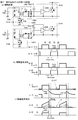
- FIG. 3 is a view for explaining current and voltage states of the high frequency insulated gate driver circuit of the present invention.
- the configuration example of FIG. 2 shows a configuration of a half bridge circuit including two switching elements on the high voltage side and the low voltage side.
- the configuration on the high voltage side for driving the switching device 50Aa on the high voltage side and the configuration on the low voltage side for driving the switching device 50Ba on the low voltage side are the same, so here the configuration for mainly driving the switching device 50Aa on the high voltage side Will be explained.
- the on / off control of the switching element 50Aa is performed by the gate driver circuit 40Aa.
- the switching element 50Aa can be configured by, for example, an RF-MOSFET, and the gate driver circuit 40Aa can be configured by an FET and a transistor in a push-pull configuration.
- the gate driver circuit 40Aa and the switching element 50Aa may be configured by a circuit in which each element is connected, in addition to being configured by one element as the high frequency switching module 2A.
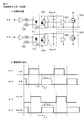
- the gate driver transformer drive element 12A constituting the input signal forming circuit 10A includes two drive elements (12A1 and 12A2).
- the gate driver transformer drive elements 12A1 and 12A2 are formed by a CMOS or TTL element having an output stage constituted by two switching elements as shown in FIG. 8A, or a circuit of a Drive IC.
- the switching element is formed of a MOS (FIG. 8 (b)) or a transistor (FIG. 8 (c)). In two switching elements connected in series, one end of each switching element is connected to power supply voltage Vcc or ground voltage, and positive and negative power supply voltages Vcc and -Vcc, and the connection point connecting both switching elements is an output stage Output the input signal S as
- the pulse signal PS-A1 (FIG. 3A) and the pulse signal PS-A2 (FIG. 3B) are input from the pulse signal forming circuit 11 to the input terminals of the gate driver transformer drive elements 12A1 and 12A2. .
- the pulse signal PS-A1 and the pulse signal PS-A2 are signals corresponding to control signals "1" and "0" of the logic element, and the gate driver transformer drive elements 12A1 and 12A2 have binary values of the pulse signal PS.
- the power supply voltage Vcc, the ground voltage, the reference voltage or the zero voltage, or the positive power supply voltage Vcc or the negative power supply voltage -Vcc is selected from the output stage and output as the input signal S.
- the pulse signals PS are complementary signals having the same duty ratio and being mutually phase shifted, and when the high potential is “1” and the low potential is “0”, the values of the mutual phases are, for example, one. “0” and the other being complementary as “1”, and “0” when the values of the respective phases are the same value, for example, both have the same value of “0” or “1”
- the values of “1” and “1” are alternately switched in time series.
- the input signal S has a voltage value corresponding to the value of the pulse signal PS. Therefore, two input signals (S) formed based on the value of pulse signal PS are complementary voltage signals having the same signal waveform as pulse signal PS and mutually shifted in phase with the same duty ratio. Phase potentials are complementary between high and low potentials, and the same potential periods where the phases have the same potential are alternated between the high and low potentials in time series. Switch to and prepare.
- One of the two outputs from the gate driver transformer drive elements 12A1 and 12A2 is input to one end of the primary side coil of the gate driver transformer 20A as an input signal S-A1 (FIG. 3 (g))
- the other output is input to the other end of the primary coil of the gate driver transformer 20A as an input signal S-A2 (FIG. 3 (h)).
- the output end of the gate driver transformer drive element 12A1 is connected to one end of both ends of the primary coil 20Aa of the gate driver transformer 20A, and the output end of the gate driver transformer drive element 12A2 is connected to the other end Be done.
- both ends of primary coil 20Aa are Vcc, -Vcc, 0
- a voltage or a voltage VT-A (FIG. 3C) at both ends of 2Vcc, -2Vcc, 0 is applied.
- the voltage VT-A across the primary side coil 20Aa can be set to Vcc, -Vcc or 0.
- the current-voltage conversion circuit 30A connects the first parallel circuit of the resistor 30Aa and the rectifying diode 30Ab and the second parallel circuit of the resistor 30Ac and the rectifying diode 30Ad in series and parallel with the secondary coil 20Ab. It consists of an impedance circuit.
- the current-voltage conversion circuit 30A converts the secondary current I2 into a positive voltage or a negative voltage according to the current direction of the secondary current I2, and performs high frequency switching as the isolated drive signal (Siso-A). Input to the gate driver circuit 40Aa of the module 2A.
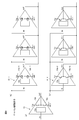
- FIG. 3D shows the primary current I1 of the exciting current im and the load current iL
- FIGS. 4 and 5 show an example of the flow of the exciting current im.
- 4 shows an example in which the voltage Vcc and the ground voltage are applied to the primary coil of the gate driver transformer
- FIG. 5 shows an example in which the positive voltage Vcc and the negative voltage -Vcc are applied to the primary coil of the gate driver transformer. Is shown.
- the solid line indicates the primary current I1 in which the excitation current im is superimposed on the load current iL
- the broken line indicates the excitation current im
- the hatched portion indicates the load current iL.
- “A”, “B”, “C”, and “D” in FIG. 3 indicate periods in which the pulse signal PS-A1 is “1” and the pulse signal PS-A2 is “0”, respectively.
- the pulse signal PS-A1 indicates “1” and the pulse signal PS-A2 indicates “1” while the pulse signal PS-A1 indicates "0” and the pulse signal PS-A2 indicates “1".
- a period in which PS-A1 is "0” and pulse signal PS-A2 is "0” is shown.
- (a) to (d) in FIG. 4 and FIG. 5 are shown corresponding to the respective periods “A” to “D”.
- Period “A” During the period “A", a positive voltage Vcc (2 Vcc in FIG. 5) is applied across the primary coil of the gate driver transformer, and a load current iL and an excitation current im flow.
- the exciting current im flows in the negative direction in the previous period “D”, and fluctuates behind the applied voltage, so in this period “A", it rises from -im to + im and flows in the positive direction.
- the load current iL flows while the voltage across the primary side coil is positive Vcc.
- the primary current I1 flowing through the primary coil is a current indicated by a solid line, and is a current obtained by combining the load current iL and the excitation current im indicated by a broken line.
- the secondary current I2 flows through the secondary coil in the direction of the arrow, and the voltage is converted by the resistor Rg2 connected in parallel, and the voltage converted is output as the insulating drive signal Siso.
- Period “B” In the period “B", the power supply voltage is applied to both terminals of the primary coil of the gate driver transformer. In this period, the load current iL does not flow because there is no voltage difference between both terminals of the primary side coil. On the other hand, since the exciting current im flows in the positive direction in the previous period “A” and there is no voltage difference between both terminals of the primary side coil, the restriction that the magnetization state of the coil is held in this period “B” The magnetization state is achieved, and the excitation current is held at the current + im at the end of the period "A".
- the primary current I1 of the primary coil is only the excitation current im indicated by the broken line.
- the secondary current I2 does not flow in the secondary side coil, and the output of the insulation drive signal Siso is zero voltage.
- Period “C” In a period “C”, a negative voltage -Vcc (-2 Vcc in FIG. 5) is applied across the primary coil of the gate driver transformer, and a load current iL and an excitation current im flow.
- the exciting current im is held in the previous period “B”, and in this period “C", it decreases from + im in the holding state and flows in the negative direction.
- the load current iL flows while the voltage across the primary side coil is negative ⁇ Vcc ( ⁇ 2 Vcc in FIG. 5).
- the primary current I1 flowing through the primary side coil is a current obtained by combining the load current iL indicated by the solid line and the excitation current im indicated by the broken line.
- the secondary current I2 flows in the direction of the arrow opposite to the period "A", and voltage conversion is performed by the resistor Rg1 connected in series.
- the isolation drive signal Siso is reverse biased by the forward voltage of the rectification diode d2 connected in parallel, and -VF for the reverse bias voltage is output.
- Period “D” In the period “D", the ground voltage (negative voltage in FIG. 5) is applied to both terminals of the primary coil of the gate driver transformer. In this period, the load current iL does not flow because there is no voltage difference between both terminals of the primary side coil. On the other hand, since the exciting current im flows in the negative direction in the previous period “C” and there is no voltage difference between both terminals of the primary side coil, the restriction that the magnetization state of the coil is held in this period “D” The magnetization state is achieved, and the excitation current is held at the current -im at the end of the period "C".
- the primary current I1 of the primary side coil is only the excitation current im indicated by the broken line.
- the secondary current I2 does not flow in the secondary side coil, and the output of the insulation drive signal Siso is zero voltage.
- the fluctuation of the load current and the excitation current is repeated with one period "A" to "D” as described above, and the excitation current always flows in the primary side coil.
- the magnetic flux state of the coil of the gate driver transformer is maintained in the constrained magnetization state controlled by the excitation current, and the gate driver transformer is always driven over the entire period in the low impedance state.
- Table 1 shows an example in which the input signals S-1 and S-2 are Vcc and the ground voltage
- Table 2 shows an example in which the input signals S-1 and S-2 are Vcc and -Vcc.
- the high frequency insulated gate driver circuit comprises the action of reverse bias effect by current-voltage conversion circuit, the action of pulse width adjustment of insulated drive signal by signal delay (phase difference) between two input signals (S), switching element Function to prevent short circuit between them and impedance matching.
- 6A and 6B show the pulse signal PS-A1 and the pulse signal PS-A2 on the high voltage side.
- the pulse signal PS-A1 and the pulse signal PS-A2 are complementary signals which have the same duty ratio and are mutually shifted in phase, and when the high potential is “1” and the low potential is “0”, one is Switch “1” and “0” alternately in a time series by switching “1” and “0” in a complementary manner that is “0” and the other is “1”. ing.
- the duty ratio shows an example of 50%, the duty ratio is not limited to 50%.
- the pulse signal PS-A1 and the pulse signal PS-A2 have a phase difference due to a delay of delay D-A with respect to the pulse signal PS-A1. Due to this phase difference, the pulse signal PS-A1 and the pulse signal PS-A2 have complementary periods in which one is “0” and the other is “1”, and both are “0” or “1”. And a certain equivalence period.
- the voltage VT-A of the primary coil of the gate driver transformer on the high voltage side has the waveform shown in FIG. -A has a voltage waveform shown in FIG.
- 6 (c) and 6 (d) show the pulse signal PS-B1 and the pulse signal PS-B2 on the low voltage side.
- the pulse signal PS-B1 and the pulse signal PS-B2 have the same relationship as the pulse signal PS-A1 and the pulse signal PS-A2, and the pulse signal PS-B2 is delayed D-B relative to the pulse signal PS-B1.
- the signal level for driving the gate driver circuit 40 is biased in the negative direction. Ru.
- the signal level for driving the gate driver circuit 40 fluctuates, Since the voltage can be prevented from rising before the gate driver circuit 4 is turned on, malfunction of the gate driver circuit 40 can be prevented.
- FIG. 6 (g) shows an insulation drive signal (Siso-A) on the high voltage side
- FIG. 6 (h) shows an insulation drive signal (Siso-B) on the low voltage side.
- the pulse width PW-A of the insulation drive signal (Siso-A) on the high voltage side is the delay between the pulse signal PS-A1 (FIG. 6 (a)) on the high voltage side and the pulse signal PS-A2 (FIG. 6 (b)) This corresponds to the phase difference due to the delay D ⁇ A. Therefore, the pulse width PW-A can be adjusted by changing the width (delay D-A) of the phase difference between the pulse signal PS-A1 on the high voltage side and the pulse signal PS-A2.
- the width (delayD-A) of the phase difference between pulse signal PS-A1 on the high voltage side and pulse signal PS-A2 is the duty ratio of pulse signal PS-A1 and pulse signal PS-A2, and pulse signal PS- on the low voltage side.
- the adjustment of the pulse width PW-A can be performed without changing the duty ratios of the pulse signals PS-A1 to PS-B2 because the parameters are independent of the duty ratio of B1 and the pulse signal PS-B2.
- the pulse width PW-B of the low voltage side isolation drive signal is the pulse signal PS-B1 (FIG. 6 (c)) and the pulse signal PS-B2 (FIG. 6 (d)) on the low voltage side.
- the pulse width PW-B by changing the width (delayD-B) of the phase difference between the pulse signal PS-B1 on the low voltage side and the pulse signal PS-B2. Can be adjusted.
- the width (delayD-B) of the phase difference between pulse signal PS-B1 on the low voltage side and pulse signal PS-B2 is the duty ratio of pulse signal PS-B1 and pulse signal PS-B2, and pulse signal PS- on the high voltage side.
- the adjustment of the pulse width PW-B can be performed without changing the duty ratios of the pulse signals PS-A1 to PS-B2 because the parameters are independent of the duty ratio of A1 and the pulse signal PS-A2.
- the period of dead time T1 corresponds to the switching time point from the conduction state of the switching element on the low voltage side to the conduction state of the switching element on the high voltage side. It is possible to prevent a short circuit.
- the high voltage side A dead time T2 is provided between the insulation drive signal (Siso-A) (FIG. 6 (g)) and the insulation drive signal (Siso-B) (FIG. 6 (h)) on the low voltage side.
- both the high voltage side isolated drive signal (Siso-A) and the low voltage side isolated drive signal (Siso-B) are in the low signal state, and the high voltage side switching element and the low voltage side Any switching element of the switching element is in a non-conductive state.
- the period of dead time T2 corresponds to the switching time point of the switching element on the high voltage side from the conducting state of the switching element on the low voltage side to the conducting state of the switching element on the low voltage side. It is possible to prevent a short circuit.
- the period of the dead time corresponds to a section in which the excitation current is held and the current is continuously supplied.
- FIG. 7 is a diagram for explaining impedance matching in the high frequency insulated gate driver circuit of the present invention.
- the impedance matching can be performed in a mode by resistance adjustment of the current-voltage conversion circuit or a mode by a common mode transformer.
- the current-voltage conversion circuits 30A and 30B include a second parallel circuit connected in parallel with the first parallel circuit connected in series.
- the primary of the gate driver transformer The input signal (S) input to the side can be transmitted as an isolation drive signal (Siso) without distortion.
- common mode transformers 81A and 81B are provided on two transmission lines 80 connected to both ends of the secondary side coil of the gate driver transformer of the high frequency insulated gate driver circuit.
- the common mode transformers 81A and 81B operate as inductors for common mode currents and do not act as inductors for differential mode currents, with the winding direction of the conductors being the same for the two transmission lines 80. , Acts as a noise filter for common mode noise current.
- the influence of the displacement voltage passed from the primary side to the secondary side can be reduced through the parasitic capacitance between the primary side and the secondary side of the gate driver transformer.
- the common mode transformers 81A and 81B are provided not only on the secondary side of the gate driver transformer as in the configuration example shown in FIG. 7, but also on the primary side of the gate driver transformer, and on the primary side and secondary side of the gate driver transformer. It is good also as composition provided in both.
- a configuration example of a gate driver transformer drive element provided in the high frequency insulated gate driver circuit of the present invention will be described with reference to FIG.
- a COMS, a TTL, and a Drive IC are formed by connecting two switching elements such as a MOS-FET and a transistor in series.
- a plurality of drive gate driver transformer drive elements can be connected in parallel.
- the switching element is not limited to the MOS-FET, and a J-FET (junction FET) can be used.
- FIG. 8 (b) and 8 (c) show a configuration in which gate driver transformer drive elements are connected in parallel, and FIG. 8 (b) shows a configuration using a MOS-FET as a gate driver transformer drive element. Shows a circuit configuration example using a transistor as a switching element.
- the high frequency insulated gate driver circuit and the gate circuit driving method of the present invention can be applied to a power conversion device such as an inverter.
Abstract
Description
(1)フォトカプラを用いた場合には、絶縁の前後で信号に位相差が生じるという問題がある。 The circuit configuration using a photocoupler as the insulating element has the following problems.
(1) When a photocoupler is used, there is a problem that a phase difference occurs in the signal before and after the insulation.
装置の態様において、本願発明の高周波絶縁ゲートドライバ回路は、互いに絶縁した高周波信号によって複数のゲート回路を駆動する。 [Aspect of device]
In the device aspect, the high frequency insulated gate driver circuit of the present invention drives multiple gate circuits with high frequency signals isolated from one another.
入力信号形成回路は、同じデューティー比で互いに位相ずれした相補の電圧信号の二つの入力信号(S)を出力する。二つの入力信号は、互いの相の電圧が高電位と低電位との相補関係である相補電位期間と、互いの相の電圧が同電位である同電位期間とを備える。二つの入力信号の各電位は、時系列で高電位と低電位とを交互に切り換わる。 (Input signal formation circuit)
The input signal forming circuit outputs two input signals (S) of complementary voltage signals which are out of phase with each other at the same duty ratio. The two input signals have complementary potential periods in which the voltages of the respective phases are in a complementary relationship between the high potential and the low potential, and the same potential periods in which the voltages of the respective phases are the same. Each potential of the two input signals alternates between high and low potentials in time series.
ゲートドライバトランス(20)は、一次側コイルの両端の各入力端子に、入力信号形成回路の各相の出力端子が接続される。ゲートドライバトランスは、入力信号(S)を入力し、この入力信号と絶縁した信号を形成する。 (Gate driver transformer)
In the gate driver transformer (20), the output terminal of each phase of the input signal forming circuit is connected to each input terminal at both ends of the primary side coil. The gate driver transformer receives an input signal (S) and forms a signal isolated from the input signal.
電流-電圧変換回路(30)は、入力端子にゲートドライバトランス(20)の出力端子が接続され、ゲートドライバトランスの二次側コイルに流れる二次電流を電流-電圧変換し、得られた絶縁駆動信号(Siso)をゲート回路に出力する。 (Current-voltage conversion circuit)
In the current-voltage conversion circuit (30), the output terminal of the gate driver transformer (20) is connected to the input terminal, and the secondary current flowing to the secondary side coil of the gate driver transformer is current-voltage converted to obtain the isolated The drive signal (Siso) is output to the gate circuit.
本願発明のゲート回路は、スイッチング素子と、スイッチング素子を駆動するゲートドライバ回路とにより高周波スイッチングモジュールを構成することができる。 (Aspect of circuit configuration)
The gate circuit of this invention can comprise a high frequency switching module with a switching element and the gate driver circuit which drives a switching element.
本願発明のゲート回路駆動方法は、複数のゲート回路を、互いに絶縁した複数の高周波信号で駆動する方法であり、ゲートドライバトランス(20)の一次側コイルの両端の各入力端子に、同じデューティー比で互いに位相ずれした相補の電圧信号であって、互いの相の電圧が高電位と低電位との相補関係である相補電位期間と、互いの相の電圧が同電位である同電位期間とを、各電位を時系列で高電位と低電位とで交互に切り換えて備える二つの入力信号(S)を印加し、ゲートドライバトランス(20)の一次側コイルにおいて、相補電位期間において励磁電流および負荷電流を流し、同電位期間において励磁電流を流し、ゲートドライバトランス(20)の二次側コイルに流れる二次電流を電流-電圧変換して得られる絶縁駆動信号(Siso)をゲート回路に入力し、絶縁駆動信号(Siso)によってゲート回路を駆動する。 [Aspect of method]
The gate circuit driving method of the present invention is a method of driving a plurality of gate circuits by a plurality of high frequency signals insulated from each other, and the same duty ratio is applied to each input terminal at both ends of the primary side coil of the gate driver transformer (20). And complementary voltage periods in which the voltages of the respective phases are complementary between the high voltage and the low voltage, and the same voltage periods in which the voltages of the respective phases are the same voltage. The two input signals (S) comprising switching each potential alternately in high and low potentials in time series are applied, and in the primary side coil of the gate driver transformer (20), excitation current and load are applied in complementary potential periods. An isolation drive signal obtained by current-voltage conversion of the secondary current flowing in the secondary side coil of the gate driver transformer (20) by flowing current and flowing excitation current in the same potential period. Enter the iso) to the gate circuit, to drive the gate circuit by an insulating drive signal (Siso).
図1は本願発明の高周波絶縁ゲートドライバ回路の概略構成を説明するための図であり、図1(a)は入力信号を形成するためのパルス信号を入力信号形成回路内で生成する構成を示し、図1(b)は入力信号を形成するためのパルス信号を入力信号形成回路外から導入する構成を示している。なお、図1は2つのスイッチング素子を備えたハーフブリッジ回路の構成例を示しているが、4つのスイッチング素子を備えたフルブリッジ回路の構成例に適応することもできる。 (Configuration of the present invention)
FIG. 1 is a view for explaining a schematic configuration of a high frequency insulated gate driver circuit of the present invention, and FIG. 1 (a) shows a configuration for generating a pulse signal for forming an input signal in an input signal forming circuit. FIG. 1 (b) shows a configuration in which a pulse signal for forming an input signal is introduced from outside the input signal forming circuit. Although FIG. 1 shows a configuration example of a half bridge circuit having two switching elements, the present invention can also be applied to a configuration example of a full bridge circuit having four switching elements.
本願発明の高周波絶縁ゲートドライバ回路の一構成例、及び本願発明の高周波絶縁ゲートドライバ回路の動作例を図2,3を用いて説明する。 (Configuration Example and Operation Example of High Frequency Insulated Gate Driver Circuit)
One configuration example of the high frequency insulated gate driver circuit of the present invention and an operation example of the high frequency insulated gate driver circuit of the present invention will be described with reference to FIGS.
次に、ゲートドライバトランスの励磁電流について、図3~5を用いて説明する。図3(d)は励磁電流im及び負荷電流iLの一次電流I1を示し、図4,5は励磁電流imの流れの一例を示している。なお、図4はゲートドライバトランスの一次側コイルに電圧Vccと接地電圧を印加した例を示し、図5はゲートドライバトランスの一次側コイルに正の電圧Vcc及び負の電圧-Vccを印加した例を示している。 (Excitation current of gate driver transformer)
Next, the excitation current of the gate driver transformer will be described with reference to FIGS. FIG. 3D shows the primary current I1 of the exciting current im and the load current iL, and FIGS. 4 and 5 show an example of the flow of the exciting current im. 4 shows an example in which the voltage Vcc and the ground voltage are applied to the primary coil of the gate driver transformer, and FIG. 5 shows an example in which the positive voltage Vcc and the negative voltage -Vcc are applied to the primary coil of the gate driver transformer. Is shown.
期間“A”では、ゲートドライバトランスの一次側コイルの両端間に正のVcc(図5では2Vcc)の電圧が印加され、負荷電流iLと励磁電流imが流れる。励磁電流imは前の期間“D”において負方向に流れており、印加電圧に対して遅れて変動するため、この期間“A”では-imから+imに上昇して正方向に流れる。負荷電流iLは、一次側コイルの両端電圧が正のVccである間流れる。 Period "A":
During the period "A", a positive voltage Vcc (2 Vcc in FIG. 5) is applied across the primary coil of the gate driver transformer, and a load current iL and an excitation current im flow. The exciting current im flows in the negative direction in the previous period "D", and fluctuates behind the applied voltage, so in this period "A", it rises from -im to + im and flows in the positive direction. The load current iL flows while the voltage across the primary side coil is positive Vcc.
期間“B”では、ゲートドライバトランスの一次側コイルの両方の端子に電源電圧が印加される。この期間では、一次側コイルの両端子間の電圧差がないため負荷電流iLは流れない。一方、励磁電流imは前の期間“A”において正の方向に流れており、一次側コイルの両端子間の電圧差がないため、この期間“B”ではコイルの磁化状態が保持される拘束磁化状態となり、励磁電流は期間“A”の終了時点の電流+imに保持される。 Period "B":
In the period "B", the power supply voltage is applied to both terminals of the primary coil of the gate driver transformer. In this period, the load current iL does not flow because there is no voltage difference between both terminals of the primary side coil. On the other hand, since the exciting current im flows in the positive direction in the previous period "A" and there is no voltage difference between both terminals of the primary side coil, the restriction that the magnetization state of the coil is held in this period "B" The magnetization state is achieved, and the excitation current is held at the current + im at the end of the period "A".
期間“C”では、ゲートドライバトランスの一次側コイルの両端間に負の-Vcc(図5では-2Vcc)の電圧が印加され、負荷電流iLと励磁電流imが流れる。励磁電流imは前の期間“B”において保持されており、この期間“C”では保持状態の+imから減少して負方向に流れる。負荷電流iLは、一次側コイルの両端電圧が負の-Vcc(図5では-2Vcc)である間流れる。 Period "C":
In a period "C", a negative voltage -Vcc (-2 Vcc in FIG. 5) is applied across the primary coil of the gate driver transformer, and a load current iL and an excitation current im flow. The exciting current im is held in the previous period "B", and in this period "C", it decreases from + im in the holding state and flows in the negative direction. The load current iL flows while the voltage across the primary side coil is negative −Vcc (−2 Vcc in FIG. 5).
期間“D”では、ゲートドライバトランスの一次側コイルの両方の端子に接地電圧が(図5では負電圧)が印加される。この期間では、一次側コイルの両端子間の電圧差がないため負荷電流iLは流れない。一方、励磁電流imは前の期間“C”において負の方向に流れており、一次側コイルの両端子間の電圧差がないため、この期間“D”ではコイルの磁化状態が保持される拘束磁化状態となり、励磁電流は期間“C”の終了時点の電流-imに保持される。 Period "D":
In the period "D", the ground voltage (negative voltage in FIG. 5) is applied to both terminals of the primary coil of the gate driver transformer. In this period, the load current iL does not flow because there is no voltage difference between both terminals of the primary side coil. On the other hand, since the exciting current im flows in the negative direction in the previous period "C" and there is no voltage difference between both terminals of the primary side coil, the restriction that the magnetization state of the coil is held in this period "D" The magnetization state is achieved, and the excitation current is held at the current -im at the end of the period "C".

次に、図6及び図7を用いて本願発明の高周波絶縁ゲートドライバ回路の作用について説明する。本願発明の高周波絶縁ゲートドライバ回路は、電流-電圧変換回路による逆バイアス効果の作用、2つの入力信号(S)間の信号遅れ(位相差)による絶縁駆動信号のパルス幅調整の作用、スイッチング素子間の短絡防止、及びインピーダンス整合の作用を奏する。 (Function of high frequency insulated gate driver circuit)
Next, the operation of the high frequency insulated gate driver circuit of the present invention will be described with reference to FIGS. 6 and 7. The high frequency insulated gate driver circuit according to the present invention comprises the action of reverse bias effect by current-voltage conversion circuit, the action of pulse width adjustment of insulated drive signal by signal delay (phase difference) between two input signals (S), switching element Function to prevent short circuit between them and impedance matching.
図6(g)に示す高圧側の絶縁駆動信号Siso-Aは、期間Cにおいて電流-電圧変換回路の整流ダイオードの順方向電圧によって逆バイアスされ負電圧-VFとなる。一方、図6(h)に示す低圧側の絶縁駆動信号Siso-Bは、期間Aにおいて電流-電圧変換回路の整流ダイオードの順方向電圧によって逆バイアスされ負電圧-VFとなる ・ Reverse bias effect of current-voltage conversion circuit:
The isolated drive signal Siso-A on the high voltage side shown in FIG. 6 (g) is reverse biased by the forward voltage of the rectifying diode of the current-voltage conversion circuit in the period C and becomes a negative voltage -VF. On the other hand, the insulation drive signal Siso-B on the low voltage side shown in FIG. 6 (h) is reverse biased by the forward voltage of the rectification diode of the current-voltage conversion circuit in period A and becomes negative voltage -VF.
図6(g)は高圧側の絶縁駆動信号(Siso-A)を示し、図6(h)は低圧側の絶縁駆動信号(Siso-B)を示している。 ・ Pulse width adjustment of isolated drive signal:
FIG. 6 (g) shows an insulation drive signal (Siso-A) on the high voltage side, and FIG. 6 (h) shows an insulation drive signal (Siso-B) on the low voltage side.
図6(a)~図6(d)において、パルス信号PS-A2の立ち下がりとパルス信号PS-A1の立ち上がりの間、及びパルス信号PS-B2の立ち上がりとパルスPS-B1の立ち下がりの間に時間幅を設けることによって、高圧側の絶縁駆動信号(Siso-A)(図6(g))と低圧側の絶縁駆動信号(Siso-B)(図6(h))との間にデットタイムT1を設ける。このデットタイムT1の期間では、高圧側の絶縁駆動信号(Siso-A)と低圧側の絶縁駆動信号(Siso-B)は共に信号レベルが低い状態にあり、高圧側のスイッチング素子及び低圧側のスイッチング素子の何れのスイッチング素子も非導通状態となる。 ・ Short circuit between switching elements:
6A to 6D, between the falling of pulse signal PS-A2 and the rising of pulse signal PS-A1, and between the rising of pulse signal PS-B2 and the falling of pulse PS-B1. By setting a time width between the high voltage side isolated drive signal (Siso-A) (FIG. 6 (g)) and the low voltage side isolated drive signal (Siso-B) (FIG. 6 (h)). A time T1 is provided. During this dead time T1, both the high voltage side insulation drive signal (Siso-A) and the low voltage side insulation drive signal (Siso-B) are in a low signal level, and the high voltage side switching element and low voltage side Any switching element of the switching element is in a non-conductive state.
図7は本願発明の高周波絶縁ゲートドライバ回路におけるインピーダンス整合を説明するための図である。 Impedance matching:
FIG. 7 is a diagram for explaining impedance matching in the high frequency insulated gate driver circuit of the present invention.
2,2A,2B 高周波スイッチングモジュール
3,3A,3B スイッチング素子駆動回路
10,10A,10B 入力信号形成回路
11,11A,11B パルス信号形成回路
12 ゲートドライバトランス駆動素子
12A,12B ゲートドライバトランス駆動素子
12A1,12A2,12B1,12B2 ゲートドライバトランス駆動素子
13 制御回路
20,20A,20B ゲートドライバトランス
20Aa 一次側コイル
20Ab 二次側コイル
30,30A,30B 電流-電圧変換回路
30Aa 抵抗
30Ab 整流ダイオード
30Ac 抵抗
30Ad 整流ダイオード
40,40A,40B,40Aa,40Ba ゲートドライバ回路
50,50A,50B,50Aa,50Ba スイッチング素子
60 負荷
70 負荷電源
80 伝送線路
81A,81B コモンモードトランス
101,101A,101B,101C,101D スイッチング素子
102,102A,102B,102C,102D ゲートドライバ回路
103 駆動電源
104 負荷
105 絶縁素子
105A,105B フォトカプラ
106,106A,106B 自由磁化トランス回路
106a トランス
106b FET
106c リセット回路
106d 整流回路
Ciso 寄生容量
I1 一次電流
I2 二次電流
iL 負荷電流
im 励磁電流
PS パルス信号
PS-A1,PS-A2,PS-B1,PS-B2 パルス信号
PW-A,PW-B パルス幅
Rg1 抵抗
Rg2 抵抗
Rline 特性インピーダンス
S,S-A,S-B,S-A1,S-A2,S-B1,S-B2 入力信号
Siso,Siso-A,Siso-B 絶縁駆動信号
T1,T2 デットタイム
Vcc 電源電圧
Vds 両端電圧
VT-A,VT-B, 両端電圧 1, 1A, 1B high frequency insulated
106c
Claims (18)
- 複数のゲート回路を、互いに絶縁した高周波信号で駆動する回路であって、
同じデューティー比で互いに位相ずれした相補の電圧信号であって、互いの相の電圧が高電位と低電位との相補関係である相補電位期間と、互いの相の電圧が同電位である同電位期間とを、各電位を時系列で高電位と低電位とで交互に切り換えて備える二つの入力信号を出力する入力信号形成回路と、
一次側コイルの両端の各入力端子に、前記入力信号形成回路10の各相の出力端子が接続されたゲートドライバトランスと、
入力端子に前記ゲートドライバトランスの出力端子が接続され、前記ゲートドライバトランスの二次側コイルに流れる二次電流を電流-電圧変換して得られる絶縁駆動信号を前記ゲート回路に出力する電流-電圧変換回路とを備え、
前記ゲートドライバトランスの一次側コイルには、前記相補電位期間において励磁電流および負荷電流が流れ、前記同電位期間において励磁電流が流れることを特徴とする、高周波絶縁ゲートドライバ回路。 A circuit for driving a plurality of gate circuits with high frequency signals isolated from one another,
Complementary voltage signals that are phase-shifted with each other at the same duty ratio, and are complementary potential periods in which the voltages of the phases are in a complementary relationship between the high and low potentials, and the same potentials where the voltages of the phases are the same. An input signal formation circuit for outputting two input signals, each of which has a period alternately switched between high potential and low potential in time series;
A gate driver transformer in which an output terminal of each phase of the input signal forming circuit 10 is connected to each input terminal at both ends of the primary coil;
An output terminal of the gate driver transformer is connected to an input terminal, and a current-voltage outputs an insulated drive signal obtained by current-voltage conversion of a secondary current flowing in a secondary coil of the gate driver transformer to the gate circuit. Equipped with a converter circuit,
An excitation current and a load current flow through the primary side coil of the gate driver transformer in the complementary potential period, and an excitation current flows in the same potential period. - 前記電流-電圧変換回路は、それぞれ抵抗と整流ダイオードとを並列接続してなる第1の並列回路と第2の並列回路とを直並列接続して構成され、
前記第1の並列回路は、前記ゲートドライバトランスの二次側コイルの巻始め側において、整流ダイオードの順方向を前記ゲート回路に向けて直列接続され、
前記第2の並列回路は、前記ゲートドライバトランスの二次側コイルの巻始め側と巻き終わり側の間において、整流ダイオードの順方向を前記ゲート回路の入力端に向けて並列接続されることを特徴とする、請求項1に記載の高周波絶縁ゲートドライバ回路。 The current-voltage conversion circuit is configured by series-parallel connection of a first parallel circuit formed by connecting a resistor and a rectification diode in parallel and a second parallel circuit.
The first parallel circuit is connected in series with the forward direction of the rectifying diode directed to the gate circuit on the winding start side of the secondary coil of the gate driver transformer.
The second parallel circuit may be connected in parallel with the forward direction of the rectifying diode toward the input end of the gate circuit between the winding start side and the winding end side of the secondary coil of the gate driver transformer. A high frequency insulated gate driver circuit according to claim 1, characterized in that. - 前記第1の並列回路及び/又は第2の並列回路は、コンデンサを並列接続することを特徴とする、請求項2に記載の高周波絶縁ゲートドライバ回路。 The high frequency insulated gate driver circuit according to claim 2, wherein the first parallel circuit and / or the second parallel circuit connect capacitors in parallel.
- 前記電流-電圧変換回路において、前記第1の並列回路の抵抗の抵抗値と前記第2の並列回路の抵抗の抵抗値は、前記ゲートドライバトランスから見た入力インピーダンスを所定値に調整することを特徴とする、請求項2に記載の高周波絶縁ゲートドライバ回路。 In the current-voltage conversion circuit, the resistance value of the resistance of the first parallel circuit and the resistance value of the resistance of the second parallel circuit adjust the input impedance viewed from the gate driver transformer to a predetermined value. A high frequency insulated gate driver circuit according to claim 2, characterized in that.
- 前記第1の並列回路の抵抗の抵抗値と前記第2の並列回路の抵抗の抵抗値は同一抵抗及び許容分を含む同等の抵抗値であることを特徴とする、請求項4に記載の高周波絶縁ゲートドライバ回路。 5. The high frequency wave according to claim 4, wherein the resistance value of the resistance of the first parallel circuit and the resistance value of the resistance of the second parallel circuit are equal resistance values including the same resistance and an allowance. Isolated gate driver circuit.
- 前記第1の並列回路の抵抗の抵抗値と前記第2の並列回路の抵抗の抵抗値は、ゲートドライバトランスと電流-電圧変換回路との間の伝送線路の特性インピーダンスと同じであることを特徴とする、請求項4に記載の高周波絶縁ゲートドライバ回路。 The resistance value of the resistance of the first parallel circuit and the resistance value of the resistance of the second parallel circuit are the same as the characteristic impedance of the transmission line between the gate driver transformer and the current-voltage conversion circuit. The high frequency insulated gate driver circuit according to claim 4, wherein
- 前記ゲートドライバトランスの一次側又は二次側にコモンモードトランスを備え、前記コモンモードトランスの特性インピーダンスは、ゲートドライバトランスと電流-電圧変換回路との間の伝送線路の特性インピーダンスと同じであることを特徴とする、1から6の何れか一つの記載の高周波絶縁ゲートドライバ回路。 A common mode transformer is provided on the primary side or secondary side of the gate driver transformer, and the characteristic impedance of the common mode transformer is the same as the characteristic impedance of the transmission line between the gate driver transformer and the current-voltage conversion circuit. 7. The high frequency insulated gate driver circuit according to any one of 1 to 6, characterized in that
- 前記入力信号形成回路は、
高周波パルス信号を形成するパルス信号形成回路と、
前記高周波パルス信号の二値に基づいて、高電位又は低電位の入力信号を出力する二つのゲートドライバトランス駆動素子を備えることを特徴とする、請求項1から7の何れか一つに記載の高周波絶縁ゲートドライバ回路。 The input signal forming circuit is
A pulse signal forming circuit for forming a high frequency pulse signal;
8. The gate driver according to claim 1, further comprising two gate driver transformer drive elements for outputting an input signal of high potential or low potential based on the binary value of the high frequency pulse signal. High frequency isolated gate driver circuit. - 高周波パルス信号を形成する制御回路を備え、
前記入力信号形成回路は、
前記制御回路が形成する高周波パルス信号の二値信号に基づいて、高電位又は低電位の入力信号を出力する二つのゲートドライバトランス駆動素子を備えることを特徴とする、請求項1から8の何れか一つに記載の高周波絶縁ゲートドライバ回路。 A control circuit for forming a high frequency pulse signal,
The input signal forming circuit is
9. The gate driver according to any one of claims 1 to 8, further comprising two gate driver transformer drive elements for outputting an input signal of high potential or low potential based on a binary signal of the high frequency pulse signal formed by the control circuit. High frequency insulated gate driver circuit according to any one. - 前記ゲート回路は、スイッチング素子と、当該スイッチング素子を駆動するゲートドライバ回路との高周波スイッチングモジュールで構成され、
前記ゲートドライバ回路は、前記電流-電圧変換回路から出力された絶縁駆動信号によって前記スイッチング素子のオン/オフ制御を行うことを特徴とする、請求項1から9の何れか一つに記載の高周波絶縁ゲートドライバ回路。 The gate circuit includes a high frequency switching module including a switching element and a gate driver circuit for driving the switching element.
10. The high frequency according to any one of claims 1 to 9, wherein the gate driver circuit performs on / off control of the switching element according to an isolation drive signal output from the current-voltage conversion circuit. Isolated gate driver circuit. - 前記複数のゲート回路は、負荷に高電位を印加する高圧側ゲート回路と負荷に低電位を印加する低圧側ゲート回路とのフルブリッジ又はハーフブリッジで構成され、
高圧側ゲート回路および低圧側ゲート回路の各入力端にそれぞれ高周波絶縁ゲートドライバ回路が接続されることを特徴とする、請求項1から10の何れか一つに記載の高周波絶縁ゲートドライバ回路。 The plurality of gate circuits are configured by a full bridge or a half bridge of a high voltage side gate circuit applying a high potential to a load and a low voltage side gate circuit applying a low potential to the load.
The high frequency insulated gate driver circuit according to any one of claims 1 to 10, wherein a high frequency insulated gate driver circuit is connected to each input terminal of the high voltage side gate circuit and the low voltage side gate circuit. - 高圧側のゲートドライバトランス駆動素子は電源電圧に基づいた前記高電位又は低電位の入力信号を形成し、
低圧側のゲートドライバトランス駆動素子は接地電圧、又は零電圧を含む基準電圧に基づいた前記高電位又は低電位の入力信号を形成することを特徴とする、請求項8又は9に記載の高周波絶縁ゲートドライバ回路。 The high side gate driver transformer drive element forms the high potential or low potential input signal based on the power supply voltage,
The high frequency insulation according to claim 8 or 9, characterized in that the low side gate driver transformer drive element forms the high potential or low potential input signal based on a ground voltage or a reference voltage including zero voltage. Gate driver circuit. - 高圧側のゲートドライバトランス駆動素子は正の電源電圧に基づいた前記高電位又は低電位の入力信号を形成し、
低圧側のゲートドライバトランス駆動素子は負の電源電圧に基づいた前記高電位又は低電位の入力信号を形成することを特徴とする、請求項8又は9に記載の高周波絶縁ゲートドライバ回路。 The high side gate driver transformer drive element forms the high or low potential input signal based on a positive power supply voltage,
10. The high frequency insulated gate driver circuit according to claim 8, wherein the low side gate driver transformer drive element forms the high potential or low potential input signal based on a negative power supply voltage. - 複数のゲート回路を、互いに絶縁した複数の高周波信号で駆動する方法であって、
ゲートドライバトランスの一次側コイルの両端の各入力端子に、同じデューティー比で互いに位相ずれした相補の電圧信号であって、互いの相の電圧が高電位と低電位との相補関係である相補電位期間と、互いの相の電圧が同電位である同電位期間とを、各電位を時系列で高電位と低電位とで交互に切り換えて備える二つの入力信号を印加し、
前記ゲートドライバトランスの一次側コイルにおいて、前記相補電位期間において励磁電流および負荷電流を流し、前記同電位期間において励磁電流を流し、
前記ゲートドライバトランスの二次側コイルに流れる二次電流を電流-電圧変換して得られる絶縁駆動信号を前記ゲート回路に入力し、
前記絶縁駆動信号によって前記ゲート回路を駆動することを特徴とする、ゲート回路駆動方法。 A method of driving a plurality of gate circuits with a plurality of high frequency signals isolated from each other,
Complementary voltage signals that are complementary in phase with each other with the same duty ratio and are complementary to each other at high voltage and low voltage at each input terminal at both ends of the primary coil of the gate driver transformer. Applying two input signals comprising a period and an equal potential period in which the voltage of each phase is the same potential by alternately switching each potential between the high potential and the low potential in time series;
In the primary side coil of the gate driver transformer, an excitation current and a load current flow in the complementary potential period, and an excitation current flows in the same potential period,
An insulation drive signal obtained by current-voltage conversion of the secondary current flowing to the secondary side coil of the gate driver transformer is input to the gate circuit,
A gate circuit driving method, comprising: driving the gate circuit by the insulation driving signal. - それぞれ抵抗と整流ダイオードとを並列接続してなる第1の並列回路と第2の並列回路とを直並列接続して構成され、
前記ゲートドライバトランスの二次側コイルの巻始め側において、抵抗と整流ダイオードとを並列接続回路であって、整流ダイオードの順方向を前記ゲート回路に向けて直列接続される第1の並列回路と、
前記ゲートドライバトランスの二次側コイルの巻始め側と巻き終わり側の間において、抵抗と整流ダイオードとを並列接続回路であって、整流ダイオードの順方向を前記ゲート回路の入力端に向けて並列接続される第2の並列回路とを直並列接続して構成され、前記ゲートドライバトランスの二次側コイルに接続された電流-電圧変換回路によって前記電流-電圧変換を行い、
前記入力信号の差電圧が前記第1の並列回路の整流ダイオードの順方向に対して負電圧である期間において、前記絶縁駆動信号の電位を前記第2の並列回路の整流ダイオードによって順方向電圧分だけ逆方向にバイアスすることを特徴とする、請求項14に記載のゲート回路駆動方法。 A first parallel circuit formed by connecting a resistor and a rectifier diode in parallel, and a second parallel circuit connected in series and in parallel;
A resistor and a rectifying diode connected in parallel on the winding start side of the secondary coil of the gate driver transformer, the first parallel circuit in which the forward direction of the rectifying diode is connected in series to the gate circuit; ,
A resistor and a rectifier diode are connected in parallel between the winding start side and the winding end side of the secondary side coil of the gate driver transformer, and the forward direction of the rectifier diode is parallel to the input end of the gate circuit. Performing the current-voltage conversion by a current-voltage conversion circuit connected in series and in parallel with a second parallel circuit to be connected, and connected to a secondary coil of the gate driver transformer;
During a period in which the differential voltage of the input signal is a negative voltage with respect to the forward direction of the rectifying diode of the first parallel circuit, the potential of the insulating drive signal is divided by the rectifying diode of the second parallel circuit. The method for driving a gate circuit according to claim 14, characterized in that only reverse bias is performed. - 二つのゲートドライバトランス駆動素子を備え、
一方のゲートドライバトランス駆動素子に、二値の高周波パルス信号の高電位の信号を印加して高電位の入力信号を生成し、
他方のゲートドライバトランス駆動素子に、二値の高周波パルス信号の低電位の信号を印加して低電位の入力信号を生成することを特徴とする、請求項14又は15に記載のゲート回路駆動方法。 Equipped with two gate driver transformer drive elements,
A high potential signal of a binary high frequency pulse signal is applied to one of the gate driver transformer drive elements to generate a high potential input signal,
The gate circuit driving method according to claim 14 or 15, wherein a low potential signal of a binary high frequency pulse signal is applied to the other gate driver transformer driving element to generate a low potential input signal. . - 前記電流-電圧変換回路から出力された絶縁駆動信号は、前記ゲート回路が備えるゲートドライバ回路により駆動電圧を生成し、当該駆動電圧によって前記ゲート回路が備えるスイッチング素子のオン/オフ制御を行うことを特徴とする、請求項14から16の何れか一つに記載のゲート回路駆動方法。 The insulated drive signal output from the current-voltage conversion circuit generates a drive voltage by a gate driver circuit included in the gate circuit, and performs on / off control of a switching element included in the gate circuit by the drive voltage. The gate circuit driving method according to any one of claims 14 to 16, characterized by:
- 前記二つの入力信号間の位相差によって絶縁駆動信号のデューティーを調整することを特徴とする、請求項14から17の何れか一つに記載のゲート回路駆動方法。 The gate circuit driving method according to any one of claims 14 to 17, wherein the duty of the insulating drive signal is adjusted by the phase difference between the two input signals.
Priority Applications (6)
| Application Number | Priority Date | Filing Date | Title |
|---|---|---|---|
| EP15880026.8A EP3220522B1 (en) | 2015-01-30 | 2015-02-20 | High-frequency-isolation gate driver circuit and gate circuit driving method |
| CN201580074222.0A CN107210667B (en) | 2015-01-30 | 2015-02-20 | High-frequency insulation gate driving circuit and grid circuit driving method |
| PL15880026T PL3220522T3 (en) | 2015-01-30 | 2015-02-20 | High-frequency-isolation gate driver circuit and gate circuit driving method |
| KR1020177021906A KR101860693B1 (en) | 2015-01-30 | 2015-02-20 | High frequency insulated gate driver circuit, and gate circuit driving method |
| US15/528,858 US10038435B2 (en) | 2015-01-30 | 2015-02-20 | High-frequency-isolation gate driver circuit and gate circuit driving method |
| TW104119273A TWI597942B (en) | 2015-01-30 | 2015-06-15 | High-frequency insulated gate driver circuit, and method for driving gate circuit |
Applications Claiming Priority (2)
| Application Number | Priority Date | Filing Date | Title |
|---|---|---|---|
| JP2015016741A JP5930560B1 (en) | 2015-01-30 | 2015-01-30 | High frequency insulated gate driver circuit and gate circuit driving method |
| JP2015-016741 | 2015-01-30 |
Publications (1)
| Publication Number | Publication Date |
|---|---|
| WO2016121131A1 true WO2016121131A1 (en) | 2016-08-04 |
Family
ID=56102904
Family Applications (1)
| Application Number | Title | Priority Date | Filing Date |
|---|---|---|---|
| PCT/JP2015/054726 WO2016121131A1 (en) | 2015-01-30 | 2015-02-20 | High-frequency-isolation gate driver circuit and gate circuit driving method |
Country Status (8)
| Country | Link |
|---|---|
| US (1) | US10038435B2 (en) |
| EP (1) | EP3220522B1 (en) |
| JP (1) | JP5930560B1 (en) |
| KR (1) | KR101860693B1 (en) |
| CN (1) | CN107210667B (en) |
| PL (1) | PL3220522T3 (en) |
| TW (1) | TWI597942B (en) |
| WO (1) | WO2016121131A1 (en) |
Families Citing this family (16)
| Publication number | Priority date | Publication date | Assignee | Title |
|---|---|---|---|---|
| JP6863337B2 (en) * | 2018-05-30 | 2021-04-21 | 横河電機株式会社 | Pulse signal output circuit |
| US10720913B1 (en) | 2019-05-28 | 2020-07-21 | Infineon Technologies Austria Ag | Integrated failsafe pulldown circuit for GaN switch |
| TWI692194B (en) * | 2019-06-27 | 2020-04-21 | 朋程科技股份有限公司 | Alternator and rectifier thereof |
| CN110545611B (en) * | 2019-08-09 | 2021-01-08 | 北京纳米维景科技有限公司 | Method for realizing grid control isolation and grid control circuit |
| US10958268B1 (en) | 2019-09-04 | 2021-03-23 | Infineon Technologies Austria Ag | Transformer-based driver for power switches |
| CN112542897B (en) * | 2019-09-23 | 2023-03-28 | 伏达半导体(合肥)股份有限公司 | H-bridge grid control equipment |
| US10979032B1 (en) | 2020-01-08 | 2021-04-13 | Infineon Technologies Austria Ag | Time-programmable failsafe pulldown circuit for GaN switch |
| CN111509954A (en) * | 2020-05-26 | 2020-08-07 | 深圳市雷能混合集成电路有限公司 | Correction control method and device for pulse width modulation signal and switching power supply |
| US20220140826A1 (en) * | 2020-10-29 | 2022-05-05 | Texas Instruments Incorporated | Temperature control for power devices |
| CN116491056A (en) * | 2020-11-06 | 2023-07-25 | 日产自动车株式会社 | Resonance type power conversion device |
| TWI792175B (en) * | 2021-02-04 | 2023-02-11 | 康舒科技股份有限公司 | Power supply device and control method thereof |
| US11264985B1 (en) * | 2021-03-04 | 2022-03-01 | Aes Global Holdings Pte Ltd. | Bipolar pulsed-voltage gate driver |
| KR20230023316A (en) * | 2021-08-10 | 2023-02-17 | 한국전기연구원 | Circuit and system for high-speed driving power semiconductor device |
| CN113794469B (en) * | 2021-09-03 | 2023-09-22 | 中国科学院电工研究所 | Frequency multiplication gate driving circuit and frequency multiplication control method thereof |
| DE102022103550B4 (en) * | 2022-02-15 | 2024-01-04 | Woco Gmbh & Co. Kg | Control circuit for an electrical separator |
| US20230268858A1 (en) * | 2022-02-23 | 2023-08-24 | Hamilton Sundstrand Corporation | Parasitic immune isolated drive |
Citations (7)
| Publication number | Priority date | Publication date | Assignee | Title |
|---|---|---|---|---|
| JPH0253279U (en) * | 1988-10-12 | 1990-04-17 | ||
| US5912810A (en) * | 1996-12-18 | 1999-06-15 | Lucent Technologies Inc. | Controller for a power switch and method of operation thereof |
| JP2002064339A (en) * | 2000-08-17 | 2002-02-28 | Taiyo Yuden Co Ltd | High frequency power amplifier |
| JP2004153882A (en) * | 2002-10-29 | 2004-05-27 | Toyota Industries Corp | Drive circuit of switching circuit |
| JP2009278863A (en) * | 2005-08-01 | 2009-11-26 | Monolithic Power Systems Inc | Insulated gate driver circuit for power switching devices |
| JP2011244615A (en) * | 2010-05-19 | 2011-12-01 | Sanken Electric Co Ltd | Driving circuit |
| JP2014200133A (en) * | 2013-03-29 | 2014-10-23 | 日本信号株式会社 | Switching power-supply device and switching semiconductor device |
Family Cites Families (16)
| Publication number | Priority date | Publication date | Assignee | Title |
|---|---|---|---|---|
| JPH0275823U (en) * | 1988-11-29 | 1990-06-11 | ||
| JP2621498B2 (en) * | 1989-08-24 | 1997-06-18 | 富士電機株式会社 | Gate drive circuit |
| JPH04114232U (en) * | 1991-03-25 | 1992-10-07 | 新神戸電機株式会社 | Gate drive circuit for insulated gate voltage-driven semiconductor devices |
| JPH04128435U (en) * | 1991-05-16 | 1992-11-24 | 三菱電機株式会社 | Isolated drive circuit for power MOS FET |
| JP2583562Y2 (en) * | 1992-06-03 | 1998-10-22 | 新電元工業株式会社 | Inverter circuit |
| JP3641785B2 (en) * | 2002-08-09 | 2005-04-27 | 株式会社京三製作所 | Power supply for plasma generation |
| US6906502B2 (en) * | 2002-11-14 | 2005-06-14 | Fyre Storm, Inc. | Method for regulating an output voltage of a power coverter |
| US7502240B2 (en) * | 2004-07-27 | 2009-03-10 | Silicon Laboratories Inc. | Distributed power supply system with separate SYNC control for controlling remote digital DC/DC converters |
| TW200717979A (en) | 2005-10-17 | 2007-05-01 | Fsp Technology Inc | Gate-driving circuit of self-driven synchronous rectifier |
| JP2008270548A (en) | 2007-04-20 | 2008-11-06 | Fuji Electric Device Technology Co Ltd | Driving unit for photocoupler, power converting device, and driving method for photocoupler |
| US9118259B2 (en) * | 2007-12-03 | 2015-08-25 | Texas Instruments Incorporated | Phase-shifted dual-bridge DC/DC converter with wide-range ZVS and zero circulating current |
| JP4790826B2 (en) * | 2009-03-10 | 2011-10-12 | 株式会社日立製作所 | Power supply device and hard disk device |
| JP5416673B2 (en) | 2010-09-30 | 2014-02-12 | 株式会社日立製作所 | Signal transmission circuit, switching element drive circuit, and power conversion device |
| EP2763307A4 (en) | 2011-09-30 | 2015-11-25 | Hitachi Ltd | Semiconductor drive circuit and power conversion apparatus using same |
| EP2712082B1 (en) | 2012-09-21 | 2015-01-07 | Ferroamp Elektronik AB | Power switch circuit with planar transformer drive |
| US9252674B2 (en) | 2012-11-26 | 2016-02-02 | System General Corp. | Transistor gate driver with charge pump circuit for offline power converters |
-
2015
- 2015-01-30 JP JP2015016741A patent/JP5930560B1/en active Active
- 2015-02-20 PL PL15880026T patent/PL3220522T3/en unknown
- 2015-02-20 US US15/528,858 patent/US10038435B2/en active Active
- 2015-02-20 KR KR1020177021906A patent/KR101860693B1/en active IP Right Grant
- 2015-02-20 CN CN201580074222.0A patent/CN107210667B/en active Active
- 2015-02-20 EP EP15880026.8A patent/EP3220522B1/en active Active
- 2015-02-20 WO PCT/JP2015/054726 patent/WO2016121131A1/en active Application Filing
- 2015-06-15 TW TW104119273A patent/TWI597942B/en active
Patent Citations (7)
| Publication number | Priority date | Publication date | Assignee | Title |
|---|---|---|---|---|
| JPH0253279U (en) * | 1988-10-12 | 1990-04-17 | ||
| US5912810A (en) * | 1996-12-18 | 1999-06-15 | Lucent Technologies Inc. | Controller for a power switch and method of operation thereof |
| JP2002064339A (en) * | 2000-08-17 | 2002-02-28 | Taiyo Yuden Co Ltd | High frequency power amplifier |
| JP2004153882A (en) * | 2002-10-29 | 2004-05-27 | Toyota Industries Corp | Drive circuit of switching circuit |
| JP2009278863A (en) * | 2005-08-01 | 2009-11-26 | Monolithic Power Systems Inc | Insulated gate driver circuit for power switching devices |
| JP2011244615A (en) * | 2010-05-19 | 2011-12-01 | Sanken Electric Co Ltd | Driving circuit |
| JP2014200133A (en) * | 2013-03-29 | 2014-10-23 | 日本信号株式会社 | Switching power-supply device and switching semiconductor device |
Also Published As
| Publication number | Publication date |
|---|---|
| TWI597942B (en) | 2017-09-01 |
| EP3220522A4 (en) | 2018-09-26 |
| US10038435B2 (en) | 2018-07-31 |
| JP2016144258A (en) | 2016-08-08 |
| US20170331471A1 (en) | 2017-11-16 |
| KR101860693B1 (en) | 2018-05-23 |
| EP3220522B1 (en) | 2019-05-01 |
| CN107210667A (en) | 2017-09-26 |
| EP3220522A1 (en) | 2017-09-20 |
| TW201628338A (en) | 2016-08-01 |
| KR20170097216A (en) | 2017-08-25 |
| PL3220522T3 (en) | 2019-08-30 |
| JP5930560B1 (en) | 2016-06-08 |
| CN107210667B (en) | 2018-05-04 |
Similar Documents
| Publication | Publication Date | Title |
|---|---|---|
| WO2016121131A1 (en) | High-frequency-isolation gate driver circuit and gate circuit driving method | |
| EP2107674A1 (en) | Half-bridge LLC resonant converter with self-driven synchronous rectifiers | |
| WO2018159437A1 (en) | Dc-dc converter | |
| US7154763B2 (en) | Push-pull switching power converter | |
| US20120320637A1 (en) | Switching power source apparatus | |
| JP2019115186A (en) | Power conversion device | |
| JP6241334B2 (en) | Current resonance type DCDC converter | |
| US20110051475A1 (en) | Regulator circuitry for reducing ripple resulted from line voltage transmitting to secondary side of power transformer | |
| JP4253650B2 (en) | Switching power supply circuit and transformer | |
| WO2014033804A1 (en) | Switching control circuit and switching power device | |
| JP4276086B2 (en) | AC-DC converter with low ripple output | |
| CN110752739B (en) | Power equipment driving device | |
| WO2016103819A1 (en) | Power conversion device | |
| US6856523B2 (en) | Level shifted drive for clamp device | |
| JP2003259644A (en) | Switching converter circuit | |
| JP2009261117A (en) | Switching power supply unit | |
| JPH07213057A (en) | Insulated element for transmission of signal | |
| WO2019187484A1 (en) | Gate drive circuit and switching device using same | |
| TWI600264B (en) | Single-switch double-group flyback converter with leakage inductance energy recovery function | |
| CN107112888B (en) | Power conversion device and method | |
| JP5544879B2 (en) | Power supply | |
| JP2001238445A (en) | Multiple-output switching power supply | |
| JP2012249441A (en) | Power conversion device | |
| JP5484818B2 (en) | Power supply | |
| JP2019110659A (en) | Multi-output insulation power supply device |
Legal Events
| Date | Code | Title | Description |
|---|---|---|---|
| 121 | Ep: the epo has been informed by wipo that ep was designated in this application |
Ref document number: 15880026 Country of ref document: EP Kind code of ref document: A1 |
|
| WWE | Wipo information: entry into national phase |
Ref document number: 15528858 Country of ref document: US |
|
| REEP | Request for entry into the european phase |
Ref document number: 2015880026 Country of ref document: EP |
|
| NENP | Non-entry into the national phase |
Ref country code: DE |
|
| ENP | Entry into the national phase |
Ref document number: 20177021906 Country of ref document: KR Kind code of ref document: A |