WO2016114232A1 - プラズマ処理装置 - Google Patents
プラズマ処理装置 Download PDFInfo
- Publication number
- WO2016114232A1 WO2016114232A1 PCT/JP2016/050510 JP2016050510W WO2016114232A1 WO 2016114232 A1 WO2016114232 A1 WO 2016114232A1 JP 2016050510 W JP2016050510 W JP 2016050510W WO 2016114232 A1 WO2016114232 A1 WO 2016114232A1
- Authority
- WO
- WIPO (PCT)
- Prior art keywords
- electrode
- frequency
- plasma processing
- power source
- chamber
- Prior art date
- Legal status (The legal status is an assumption and is not a legal conclusion. Google has not performed a legal analysis and makes no representation as to the accuracy of the status listed.)
- Ceased
Links
Images





Classifications
-
- H—ELECTRICITY
- H01—ELECTRIC ELEMENTS
- H01J—ELECTRIC DISCHARGE TUBES OR DISCHARGE LAMPS
- H01J37/00—Discharge tubes with provision for introducing objects or material to be exposed to the discharge, e.g. for the purpose of examination or processing thereof
- H01J37/32—Gas-filled discharge tubes
- H01J37/32009—Arrangements for generation of plasma specially adapted for examination or treatment of objects, e.g. plasma sources
- H01J37/32082—Radio frequency generated discharge
- H01J37/321—Radio frequency generated discharge the radio frequency energy being inductively coupled to the plasma
-
- H—ELECTRICITY
- H01—ELECTRIC ELEMENTS
- H01J—ELECTRIC DISCHARGE TUBES OR DISCHARGE LAMPS
- H01J17/00—Gas-filled discharge tubes with solid cathode
- H01J17/02—Details
- H01J17/04—Electrodes; Screens
-
- H—ELECTRICITY
- H01—ELECTRIC ELEMENTS
- H01J—ELECTRIC DISCHARGE TUBES OR DISCHARGE LAMPS
- H01J37/00—Discharge tubes with provision for introducing objects or material to be exposed to the discharge, e.g. for the purpose of examination or processing thereof
- H01J37/32—Gas-filled discharge tubes
- H01J37/32431—Constructional details of the reactor
- H01J37/32532—Electrodes
- H01J37/32568—Relative arrangement or disposition of electrodes; moving means
-
- H—ELECTRICITY
- H05—ELECTRIC TECHNIQUES NOT OTHERWISE PROVIDED FOR
- H05H—PLASMA TECHNIQUE; PRODUCTION OF ACCELERATED ELECTRICALLY-CHARGED PARTICLES OR OF NEUTRONS; PRODUCTION OR ACCELERATION OF NEUTRAL MOLECULAR OR ATOMIC BEAMS
- H05H1/00—Generating plasma; Handling plasma
- H05H1/24—Generating plasma
- H05H1/26—Plasma torches
- H05H1/32—Plasma torches using an arc
- H05H1/34—Details, e.g. electrodes, nozzles
- H05H1/38—Guiding or centering of electrodes
-
- H—ELECTRICITY
- H05—ELECTRIC TECHNIQUES NOT OTHERWISE PROVIDED FOR
- H05H—PLASMA TECHNIQUE; PRODUCTION OF ACCELERATED ELECTRICALLY-CHARGED PARTICLES OR OF NEUTRONS; PRODUCTION OR ACCELERATION OF NEUTRAL MOLECULAR OR ATOMIC BEAMS
- H05H1/00—Generating plasma; Handling plasma
- H05H1/24—Generating plasma
- H05H1/46—Generating plasma using applied electromagnetic fields, e.g. high frequency or microwave energy
-
- H—ELECTRICITY
- H10—SEMICONDUCTOR DEVICES; ELECTRIC SOLID-STATE DEVICES NOT OTHERWISE PROVIDED FOR
- H10P—GENERIC PROCESSES OR APPARATUS FOR THE MANUFACTURE OR TREATMENT OF DEVICES COVERED BY CLASS H10
- H10P14/00—Formation of materials, e.g. in the shape of layers or pillars
- H10P14/60—Formation of materials, e.g. in the shape of layers or pillars of insulating materials
- H10P14/65—Formation of materials, e.g. in the shape of layers or pillars of insulating materials characterised by treatments performed before or after the formation of the materials
- H10P14/6502—Formation of materials, e.g. in the shape of layers or pillars of insulating materials characterised by treatments performed before or after the formation of the materials of treatments performed before formation of the materials
- H10P14/6512—Formation of materials, e.g. in the shape of layers or pillars of insulating materials characterised by treatments performed before or after the formation of the materials of treatments performed before formation of the materials by exposure to a gas or vapour
- H10P14/6514—Formation of materials, e.g. in the shape of layers or pillars of insulating materials characterised by treatments performed before or after the formation of the materials of treatments performed before formation of the materials by exposure to a gas or vapour by exposure to a plasma
-
- H—ELECTRICITY
- H10—SEMICONDUCTOR DEVICES; ELECTRIC SOLID-STATE DEVICES NOT OTHERWISE PROVIDED FOR
- H10P—GENERIC PROCESSES OR APPARATUS FOR THE MANUFACTURE OR TREATMENT OF DEVICES COVERED BY CLASS H10
- H10P14/00—Formation of materials, e.g. in the shape of layers or pillars
- H10P14/60—Formation of materials, e.g. in the shape of layers or pillars of insulating materials
- H10P14/65—Formation of materials, e.g. in the shape of layers or pillars of insulating materials characterised by treatments performed before or after the formation of the materials
- H10P14/6516—Formation of materials, e.g. in the shape of layers or pillars of insulating materials characterised by treatments performed before or after the formation of the materials of treatments performed after formation of the materials
- H10P14/6529—Formation of materials, e.g. in the shape of layers or pillars of insulating materials characterised by treatments performed before or after the formation of the materials of treatments performed after formation of the materials by exposure to a gas or vapour
- H10P14/6532—Formation of materials, e.g. in the shape of layers or pillars of insulating materials characterised by treatments performed before or after the formation of the materials of treatments performed after formation of the materials by exposure to a gas or vapour by exposure to a plasma
-
- H—ELECTRICITY
- H10—SEMICONDUCTOR DEVICES; ELECTRIC SOLID-STATE DEVICES NOT OTHERWISE PROVIDED FOR
- H10P—GENERIC PROCESSES OR APPARATUS FOR THE MANUFACTURE OR TREATMENT OF DEVICES COVERED BY CLASS H10
- H10P50/00—Etching of wafers, substrates or parts of devices
- H10P50/20—Dry etching; Plasma etching; Reactive-ion etching
- H10P50/24—Dry etching; Plasma etching; Reactive-ion etching of semiconductor materials
- H10P50/242—Dry etching; Plasma etching; Reactive-ion etching of semiconductor materials of Group IV materials
-
- H—ELECTRICITY
- H10—SEMICONDUCTOR DEVICES; ELECTRIC SOLID-STATE DEVICES NOT OTHERWISE PROVIDED FOR
- H10P—GENERIC PROCESSES OR APPARATUS FOR THE MANUFACTURE OR TREATMENT OF DEVICES COVERED BY CLASS H10
- H10P50/00—Etching of wafers, substrates or parts of devices
- H10P50/20—Dry etching; Plasma etching; Reactive-ion etching
- H10P50/26—Dry etching; Plasma etching; Reactive-ion etching of conductive or resistive materials
- H10P50/264—Dry etching; Plasma etching; Reactive-ion etching of conductive or resistive materials by chemical means
- H10P50/266—Dry etching; Plasma etching; Reactive-ion etching of conductive or resistive materials by chemical means by vapour etching only
- H10P50/267—Dry etching; Plasma etching; Reactive-ion etching of conductive or resistive materials by chemical means by vapour etching only using plasmas
-
- H—ELECTRICITY
- H01—ELECTRIC ELEMENTS
- H01J—ELECTRIC DISCHARGE TUBES OR DISCHARGE LAMPS
- H01J2237/00—Discharge tubes exposing object to beam, e.g. for analysis treatment, etching, imaging
- H01J2237/02—Details
- H01J2237/0203—Protection arrangements
- H01J2237/0206—Extinguishing, preventing or controlling unwanted discharges
-
- H—ELECTRICITY
- H05—ELECTRIC TECHNIQUES NOT OTHERWISE PROVIDED FOR
- H05H—PLASMA TECHNIQUE; PRODUCTION OF ACCELERATED ELECTRICALLY-CHARGED PARTICLES OR OF NEUTRONS; PRODUCTION OR ACCELERATION OF NEUTRAL MOLECULAR OR ATOMIC BEAMS
- H05H1/00—Generating plasma; Handling plasma
- H05H1/24—Generating plasma
- H05H1/2406—Generating plasma using dielectric barrier discharges, i.e. with a dielectric interposed between the electrodes
- H05H1/2443—Generating plasma using dielectric barrier discharges, i.e. with a dielectric interposed between the electrodes the plasma fluid flowing through a dielectric tube
- H05H1/2465—Generating plasma using dielectric barrier discharges, i.e. with a dielectric interposed between the electrodes the plasma fluid flowing through a dielectric tube the plasma being activated by inductive coupling, e.g. using coiled electrodes
-
- H—ELECTRICITY
- H05—ELECTRIC TECHNIQUES NOT OTHERWISE PROVIDED FOR
- H05H—PLASMA TECHNIQUE; PRODUCTION OF ACCELERATED ELECTRICALLY-CHARGED PARTICLES OR OF NEUTRONS; PRODUCTION OR ACCELERATION OF NEUTRAL MOLECULAR OR ATOMIC BEAMS
- H05H1/00—Generating plasma; Handling plasma
- H05H1/24—Generating plasma
- H05H1/46—Generating plasma using applied electromagnetic fields, e.g. high frequency or microwave energy
- H05H1/4645—Radiofrequency discharges
- H05H1/4652—Radiofrequency discharges using inductive coupling means, e.g. coils
Definitions
- the present invention relates to a plasma processing apparatus capable of stabilizing in low frequency discharge.
- a trench structure with a deep groove or a through hole with a large aspect ratio is formed on a semiconductor substrate by a dry etching method.
- a plasma processing apparatus having a counter electrode is widely used (for example, Patent Document 1).
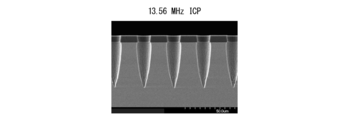
- FIG. 5A and 5B are SEM photographs showing cross-sectional shapes of non-through holes formed by applying AC voltages of different frequencies to the counter electrode.
- FIG. 5A is a SEM photograph showing a case where the frequency is 13.56 MHz
- FIG. 5B is a case where the frequency is 2 MHz.
- Both FIG. 5A and FIG. 5B are the results of etching processing so that the diameter of the hole is 10 ⁇ m.
- the case where the frequency is 13.56 MHz (FIG. 5A)
- the case where the frequency is 2 MHz enables deeper etching, and the variation in the inner diameter in the vicinity of the opening is small, and the favorable hole shape It can be seen that
- FIG. 6 is a graph showing a result of spectroscopic measurement of light emission of plasma generated when alternating voltages of different frequencies are applied to the counter electrode, where the horizontal axis represents applied power [W] and the vertical axis represents F radical emission. It is strength.
- F radicals are particles observed in plasma generated by using a process gas containing fluorine (F).
- FIG. 7 shows a configuration example in which the frequency of the AC power source is 2 MHz. However, when an AC power source having a frequency of 13.56 MHz is used, the result of FIG. 6 can be obtained by replacing the AC power source at the same position. Obtained.
- the discharge region ranges from a region where the F radical emission intensity is low (glow discharge region) to a region where the F radical emission intensity is high (inductive discharge region). Migrate to At that time, a mode jump region where the discharge is switched exists between the two regions. Due to the presence of this mode jump region, the induction discharge region has a problem of requiring a manual adjustment time of about 1 minute until the discharge is stabilized.
- the present invention has been devised in view of such conventional circumstances, and provides a plasma processing apparatus that can stably use excellent etching characteristics in an induction discharge region without being affected by a mode jump region.
- the purpose is to do.
- a plasma processing apparatus is capable of decompressing an inside thereof, and is configured to be plasma-processed on an object to be processed therein, and is disposed in the chamber.
- a spiral second electrode arranged to face the first electrode across a quartz plate forming an upper lid of the chamber, and a gas inlet arranged in the upper lid or in the vicinity thereof
- Gas introduction means for introducing a process gas containing fluorine into the chamber, a second high-frequency power source for applying an alternating voltage of a second frequency to the second electrode, and the second frequency Higher third frequency
- a third high-frequency power source for applying an alternating voltage are electrically connected, two kinds of alternating voltages is configured to be applied at the same time.
- the second electrode is disposed at a spiral center end, disposed at a spiral outer peripheral end, and a first portion that applies a high frequency from the second power source, and is grounded to ground.
- the third portion may be disposed in an outermost peripheral region forming a spiral shape in the intermediate region of the second electrode.
- the spiral second electrode includes a first circumference having a specific radius, a second circumference having a radius larger than the specific radius, the first circumference, and the A spiral shape may be formed by repeatedly arranging a connection portion connecting the second circulation portion.
- the second frequency of the second power source connected to the second electrode may be 2 MHz
- the third frequency of the third power source may be 13.56 MHz.
- the high-frequency power source B that applies an alternating voltage of the frequency ⁇ b to the second electrode disposed to face the first electrode on which the object is placed, and the frequency ⁇ c higher than the ⁇ b.
- a high-frequency power source C for applying an alternating voltage is electrically connected to the second electrode, and two kinds of alternating voltages can be applied simultaneously.
- the second electrode is always in a state where AC voltages of different frequencies ⁇ b and ⁇ c are superimposed. Therefore, even if one frequency ⁇ b is an AC voltage having a frequency that generates a mode jump region, an AC voltage having a frequency that does not generate a mode jump region is selected as the other frequency ⁇ c, and a combination of both is selected. It becomes possible to eliminate the influence of. Therefore, the above aspect of the present invention provides a plasma processing apparatus that can stably use excellent etching characteristics in the induction discharge region without being affected by the mode jump region.
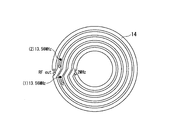
- FIG. 1 It is sectional drawing which shows an example of the plasma processing apparatus which concerns on one Embodiment of this invention. It is a top view which shows an example of the connection position of the power supply B and the power supply C with respect to a 2nd electrode. It is a top view which shows another example of the connection position of the power supply B and the power supply C with respect to a 2nd electrode. It is a top view which shows another example of the connection position of the power supply B and the power supply C with respect to a 2nd electrode. It is a cross-sectional SEM photograph of the non-through-hole produced with the plasma processing apparatus of FIG. It is a cross-sectional SEM photograph of the non-through-hole produced with the conventional plasma processing apparatus.
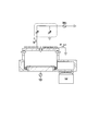
- the plasma processing apparatus 10 in FIG. 1 is an apparatus that performs plasma processing on the workpiece S in a chamber 11 that can be depressurized by, for example, the exhaust means TMP.
- the plasma processing apparatus 10 of this embodiment includes a chamber 11, a flat plate-like first electrode (support means) 12, a high-frequency power source A, an upper lid 13, a spiral second electrode (antenna) 14, and gas introduction. It has a mouth (15a, 15b, 15c) and a gas introduction means (not shown).
- the first electrode (support means) 12 is disposed in the chamber 11 and places the object S to be processed.
- the high frequency power source (first high frequency power source) A can apply a bias voltage having a frequency (first frequency) ⁇ a to the first electrode 12.
- the spiral second electrode (antenna) 14 is disposed outside the chamber 11 and is disposed so as to face the first electrode 12 with a quartz plate forming the upper lid 13 of the chamber 11 interposed therebetween.
- the gas introduction means introduces a process gas G containing fluorine (F) into the chamber 11 from the gas introduction port 15 (15a, 15b, 15c) arranged in the upper lid 13 or the vicinity thereof (upper part of the chamber 11). To do.
- a high frequency power source (second high frequency power source) B that applies an AC voltage having a frequency (second frequency) ⁇ b (2 MHz) to the second electrode 14, and a frequency higher than the ⁇ b.
- a high-frequency power source (third high-frequency power source) C that applies an AC voltage of (third frequency) ⁇ c (13.56 MHz) is electrically connected.
- the high frequency power source B applies an AC voltage having a frequency ⁇ b (2 MHz) to the second electrode 14.
- the high frequency power supply C applies an AC voltage having a frequency ⁇ c (13.56 MHz) higher than ⁇ b to the second electrode 14. That is, the plasma processing apparatus 10 of the present embodiment is configured such that two types of alternating voltages can be applied simultaneously to the second electrode 14. And as shown in FIG. 1, after passing through a matching box (M / B) and a filter (Filter), the structure by which each alternating voltage is applied with respect to the 2nd electrode 14 is preferable.
- the second electrode 14 can always have a state in which alternating voltages of different frequencies ⁇ b and ⁇ c are superimposed. Therefore, even if one frequency ⁇ b is an AC voltage having a frequency that generates a mode jump region, an AC voltage having a frequency that does not generate a mode jump region can be selected as the other frequency ⁇ c. By combining both, it is possible to eliminate the influence of the mode jump area. Therefore, the plasma processing apparatus 10 according to the present embodiment can stably use the excellent etching characteristics in the induction discharge region without being affected by the mode jump region.
- Examples of the “target object S” in the present embodiment include silicon and silicon dioxide.
- Examples of the “process gas G containing fluorine (F)” in the present embodiment include SF 6 , C 4 F 8 , C 3 F 8 , CF 4 , CHF 3 , BF 3 , NF 3 , and SiF 4. It is done.
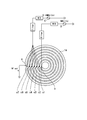
- FIG. 2 is a plan view illustrating an example of a connection position of the power source B and the power source C to the second electrode.
- a portion (third portion) c (c1 to c7) is arranged in an intermediate region located between the outer peripheral edge and the outer peripheral end.
- the part b applies a high-frequency AC voltage from the power source B to the second electrode 14.
- the part e is grounded to the ground.
- the part c applies a high-frequency AC voltage from the power source C to the second electrode 14.
- the part c is disposed in the outermost peripheral region (region extending from c7 to e) forming a spiral shape in the intermediate region of the second electrode 14.
- the process plasma generation by the low frequency ⁇ b that determines the etching process characteristics can be performed on most of the second electrode 14 from c7 to c1 (part b).
- the plasma generation region by the high frequency ⁇ c which only generates auxiliary plasma in the process, can be retained at the outer edge of the second electrode 14 from c7 to e.
- the spiral second electrode 14 is formed in a spiral shape by repeatedly arranging a circumferential portion (first circumferential portion) ⁇ , a circumferential portion (second circumferential portion) ⁇ , and a connection portion S. It is preferable to have the structure to do.
- the circular portion ⁇ has a specific radius.
- the circular portion ⁇ has a radius larger than the specific radius.
- the connecting portion S connects the circulating portion ⁇ and the circulating portion ⁇ . According to this configuration, it is possible to suppress the current flowing through the inner line (circular portion ⁇ ) from being concentrated on the connection portion S. Therefore, in the plasma processing apparatus including the second electrode 14 functioning as a high-frequency antenna as shown in FIG. 2, the second electrode 14 is locally heated to damage a part of the second electrode 14.
- the number in which the circulation part ⁇ , the circulation part ⁇ , and the connection part S are repeatedly arranged is not particularly limited.
- the frequency ⁇ b of the power source B connected to the second electrode 14 is 2 [MHz] and the frequency ⁇ c of the power source C is 13.56 [MHz]. According to this configuration, by using ⁇ c, it is possible to obtain a configuration that ensures a function capable of stable discharge without any mode jump.
- the second electrode in the present embodiment may have a configuration in which a region where the second electrode 14 does not exist occupies a large area at the center of the spiral second electrode 14. According to this configuration, when optimization of the etching in-plane distribution is not desired, if it is not desirable that process plasma generation exists in the central portion, the RF loss is reduced particularly by shortening the length of the second electrode. More efficient ICP discharge can be realized.
- the second electrode in the present embodiment may have a configuration in which a region where the second electrode 14 does not exist occupies a small area at the center of the spiral second electrode 14. According to this configuration, when the etching in-plane distribution is optimized, it is possible to cope with the case where it is desirable that process plasma generation exists in the central portion.
- FIG. 4 is a cross-sectional SEM photograph of a non-through hole produced by the plasma processing apparatus of FIG. It was confirmed that by using the plasma processing apparatus of the present embodiment, a sharp deep digging non-through hole can be produced without being affected by the mode jump region, as in the conventional plasma processing apparatus. Therefore, according to the plasma processing apparatus of the present embodiment, excellent etching characteristics in the induction discharge region can be stably used without being affected by the mode jump region. Therefore, this embodiment contributes to construction of a production line having high mass productivity.
- the present invention is widely applicable to plasma processing apparatuses.
- a high frequency power supply (first high frequency power supply), B high frequency power supply (second high frequency power supply), C high frequency power supply (third high frequency power supply), G process gas, M / B matching box, S workpiece, TMP exhaust Means, ⁇ a frequency (first frequency), ⁇ b frequency (second frequency), ⁇ c frequency (third frequency), 10 plasma processing apparatus, 11 chamber, 12 first electrode (support means), 13 upper lid, 14 Second electrode (antenna), 15 (15a, 15b, 15c) gas inlet, b part (first part), e part (second part), c part (third part), ⁇ circulating part ( (First circuit part), ⁇ circuit part (second circuit part), S connection part.
Landscapes
- Physics & Mathematics (AREA)
- Engineering & Computer Science (AREA)
- Plasma & Fusion (AREA)
- Spectroscopy & Molecular Physics (AREA)
- Chemical & Material Sciences (AREA)
- Analytical Chemistry (AREA)
- Electromagnetism (AREA)
- Plasma Technology (AREA)
- Drying Of Semiconductors (AREA)
Abstract
Description
本願は、2015年1月16日に日本に出願された特願2015-006728号に基づき優先権を主張し、その内容をここに援用する。
上記一態様において、前記第二電極は、螺旋状の中心端に配置され、前記第二の電源から高周波を印加する第一の部位と、螺旋状の外周端に配置され、アースに接地される第二の部位と、螺旋状の前記中心端と前記外周端との間に位置する中間領域に配置され、前記第三の電源から高周波を印加する第三の部位と、を有してもよい。
上記一態様において、前記第三の部位が、前記第二電極の前記中間領域のうち、螺旋状を形成する最外周領域に配置されていてもよい。
上記一態様において、前記螺旋状の第二電極が、特定の半径を有する第一の周回部と、前記特定の半径より大きな半径を有する第二の周回部と、前記第一の周回部と前記第二の周回部とを繋ぐ接続部とを繰り返し配置することにより、螺旋状を形成していてもよい。
上記一態様において、前記第二電極に接続される、前記第二の電源の前記第二の周波数が2MHz、前記第三の電源の前記第三の周波数が13.56MHzであってもよい。
したがって、本発明の上記態様は、モードジャンプ領域の影響を受けることなく、誘導放電領域における優れたエッチング特性を安定して利用できる、プラズマ処理装置をもたらす。
本実施形態のプラズマ処理装置10は、チャンバ11と、平板状の第一電極(支持手段)12と、高周波電源Aと、上蓋13と、螺旋状の第二電極(アンテナ)14と、ガス導入口(15a、15b、15c)と、ガス導入手段(不図示)と、を備えている。第一電極(支持手段)12は、チャンバ11内に配され、被処理体Sを載置する。高周波電源(第一の高周波電源)Aは、第一電極12に対して、周波数(第一の周波数)λaのバイアス電圧を印加可能である。螺旋状の第二電極(アンテナ)14は、チャンバ11外に配され、チャンバ11の上蓋13を形成する石英板を挟んで、第一電極12と対向するように配置される。ガス導入手段は、前記上蓋13あるいはその近傍(チャンバ11の上部)に配されたガス導入口15(15a、15b、15c)から、チャンバ11内にフッ素(F)を含有するプロセスガスGを導入する。
本実施形態における「フッ素(F)を含有するプロセスガスG」としては、たとえば、SF6、C4F8、C3F8、CF4、CHF3、BF3、NF3、SiF4が挙げられる。
図2に示すように、前記第二電極14において、螺旋状の中心端に部位(第一の部位)b、螺旋状の外周端に部位(第二の部位)e、螺旋状の該中心端と該外周端との間に位置する中間領域に、部位(第三の部位)c(c1~c7)が配置されている。部位bは、前記電源Bから高周波の交流電圧を第二電極14に印加する。部位eは、アースに接地される。部位cは、前記電源Cから高周波の交流電圧を第二電極14に印加する。
本実施形態における第二電極は、図3Aに示すように、前記螺旋状の第二電極14の中央部に、第二電極14が存在しない領域が大きな面積を占める構成を有しても良い。この構成によれば、エッチング面内分布の最適化を行う際に、中央部にプロセスプラズマ生成が存在することが望ましくない場合は、特に第二電極の長さが短くなることでRF損失の少ないより高効率なICP放電を実現できる。
本実施形態のプラズマ処理装置を用いることにより、モードジャンプ領域の影響を受けること無く、従来のプラズマ処理装置と同様に、シャープな深掘り形状の非貫通孔を作製できることが確認された。
したがって、本実施形態のプラズマ処理装置によれば、モードジャンプ領域の影響を受けることなく、誘導放電領域における優れたエッチング特性を安定して利用できる。ゆえに、本実施形態は、高い量産性をもった製造ラインの構築に寄与する。
Claims (5)
- プラズマ処理装置であって、
その内部の減圧が可能で、前記内部で被処理体に対してプラズマ処理されるように構成されるチャンバと、
前記チャンバ内に配され、前記被処理体を載置する平板状の第一電極と、
前記第一電極に対して、第一の周波数のバイアス電圧が印加されるように構成された第一の高周波電源と、
前記チャンバ外に配置され、前記チャンバの上蓋を形成する石英板を挟んで、前記第一電極と対向するように配置された螺旋状の第二電極と、
前記上蓋あるいはその近傍に配置されたガス導入口から、前記チャンバ内にフッ素を含有するプロセスガスを導入するガス導入手段と、を備え、
前記第二電極に対して、第二の周波数の交流電圧を印加する第二の高周波電源と、前記第二の周波数より高い第三の周波数の交流電圧を印加する第三の高周波電源とが、電気的に接続されており、2種類の交流電圧が同時に印加されるように構成されているプラズマ処理装置。 - 前記第二電極は、螺旋状の中心端に配置され、前記第二の電源から高周波を印加する第一の部位と、螺旋状の外周端に配置され、アースに接地される第二の部位と、螺旋状の前記中心端と前記外周端との間に位置する中間領域に配置され、前記第三の電源から高周波を印加する第三の部位と、を有する請求項1に記載のプラズマ処理装置。
- 前記第三の部位が、前記第二電極の前記中間領域のうち、螺旋状を形成する最外周領域に配置されている請求項2に記載のプラズマ処理装置。
- 前記螺旋状の第二電極が、特定の半径を有する第一の周回部と、前記特定の半径より大きな半径を有する第二の周回部と、前記第一の周回部と前記第二の周回部とを繋ぐ接続部とを繰り返し配置することにより、螺旋状を形成している請求項1乃至3のいずれか一項に記載のプラズマ処理装置。
- 前記第二電極に接続される、前記第二の電源の前記第二の周波数が2MHz、前記第三の電源の前記第三の周波数が13.56MHzである請求項1乃至4のいずれか一項に記載のプラズマ処理装置。
Priority Applications (5)
| Application Number | Priority Date | Filing Date | Title |
|---|---|---|---|
| KR1020167033046A KR101721431B1 (ko) | 2015-01-16 | 2016-01-08 | 플라즈마 처리 장치 |
| SG11201609947WA SG11201609947WA (en) | 2015-01-16 | 2016-01-08 | Plasma processing device |
| JP2016543086A JP6013666B1 (ja) | 2015-01-16 | 2016-01-08 | プラズマ処理装置 |
| US15/314,772 US10079133B2 (en) | 2015-01-16 | 2016-01-08 | Plasma processing device |
| CN201680001490.4A CN106463393B (zh) | 2015-01-16 | 2016-01-08 | 等离子体处理装置 |
Applications Claiming Priority (2)
| Application Number | Priority Date | Filing Date | Title |
|---|---|---|---|
| JP2015-006728 | 2015-01-16 | ||
| JP2015006728 | 2015-01-16 |
Publications (1)
| Publication Number | Publication Date |
|---|---|
| WO2016114232A1 true WO2016114232A1 (ja) | 2016-07-21 |
Family
ID=56405779
Family Applications (1)
| Application Number | Title | Priority Date | Filing Date |
|---|---|---|---|
| PCT/JP2016/050510 Ceased WO2016114232A1 (ja) | 2015-01-16 | 2016-01-08 | プラズマ処理装置 |
Country Status (7)
| Country | Link |
|---|---|
| US (1) | US10079133B2 (ja) |
| JP (1) | JP6013666B1 (ja) |
| KR (1) | KR101721431B1 (ja) |
| CN (1) | CN106463393B (ja) |
| SG (1) | SG11201609947WA (ja) |
| TW (1) | TWI683341B (ja) |
| WO (1) | WO2016114232A1 (ja) |
Cited By (2)
| Publication number | Priority date | Publication date | Assignee | Title |
|---|---|---|---|---|
| JP2021509557A (ja) * | 2017-12-29 | 2021-03-25 | ラム リサーチ コーポレーションLam Research Corporation | 高電力無線周波数の螺旋コイルフィルタ |
| KR20240001060A (ko) | 2022-06-24 | 2024-01-03 | 가부시키가이샤 아루박 | 플라스마 처리 장치 및 플라스마 처리 방법 |
Families Citing this family (1)
| Publication number | Priority date | Publication date | Assignee | Title |
|---|---|---|---|---|
| WO2019078126A1 (ja) * | 2017-10-16 | 2019-04-25 | 株式会社アルバック | プラズマ処理装置 |
Citations (4)
| Publication number | Priority date | Publication date | Assignee | Title |
|---|---|---|---|---|
| JPH0982495A (ja) * | 1995-09-18 | 1997-03-28 | Toshiba Corp | プラズマ生成装置およびプラズマ生成方法 |
| JP2003017473A (ja) * | 2001-06-29 | 2003-01-17 | Toshiba Corp | プラズマ処理装置とプラズマ処理方法および半導体装置の製造方法 |
| JP2003243369A (ja) * | 2002-02-15 | 2003-08-29 | Matsushita Electric Ind Co Ltd | プラズマ処理方法及び装置 |
| JP2012074464A (ja) * | 2010-09-28 | 2012-04-12 | Tokyo Electron Ltd | プラズマ処理装置 |
Family Cites Families (11)
| Publication number | Priority date | Publication date | Assignee | Title |
|---|---|---|---|---|
| US5965034A (en) | 1995-12-04 | 1999-10-12 | Mc Electronics Co., Ltd. | High frequency plasma process wherein the plasma is executed by an inductive structure in which the phase and anti-phase portion of the capacitive currents between the inductive structure and the plasma are balanced |
| US6164241A (en) | 1998-06-30 | 2000-12-26 | Lam Research Corporation | Multiple coil antenna for inductively-coupled plasma generation systems |
| US6597117B2 (en) * | 2001-11-30 | 2003-07-22 | Samsung Austin Semiconductor, L.P. | Plasma coil |
| TWI241868B (en) | 2002-02-06 | 2005-10-11 | Matsushita Electric Industrial Co Ltd | Plasma processing method and apparatus |
| JP5227245B2 (ja) * | 2009-04-28 | 2013-07-03 | 東京エレクトロン株式会社 | プラズマ処理装置 |
| JP5643062B2 (ja) * | 2009-11-24 | 2014-12-17 | 東京エレクトロン株式会社 | プラズマ処理装置 |
| JP5554099B2 (ja) * | 2010-03-18 | 2014-07-23 | 東京エレクトロン株式会社 | プラズマ処理装置及びプラズマ処理方法 |
| JP5800547B2 (ja) * | 2011-03-29 | 2015-10-28 | 東京エレクトロン株式会社 | プラズマ処理装置及びプラズマ処理方法 |
| JP2012248578A (ja) | 2011-05-25 | 2012-12-13 | Ulvac Japan Ltd | プラズマエッチング装置 |
| US9161428B2 (en) * | 2012-04-26 | 2015-10-13 | Applied Materials, Inc. | Independent control of RF phases of separate coils of an inductively coupled plasma reactor |
| EP2913422B1 (en) * | 2012-10-23 | 2020-04-01 | Shincron Co., Ltd. | Thin film formation apparatus and method of forming thin film |
-
2016
- 2016-01-08 JP JP2016543086A patent/JP6013666B1/ja active Active
- 2016-01-08 KR KR1020167033046A patent/KR101721431B1/ko active Active
- 2016-01-08 SG SG11201609947WA patent/SG11201609947WA/en unknown
- 2016-01-08 CN CN201680001490.4A patent/CN106463393B/zh active Active
- 2016-01-08 WO PCT/JP2016/050510 patent/WO2016114232A1/ja not_active Ceased
- 2016-01-08 US US15/314,772 patent/US10079133B2/en active Active
- 2016-01-14 TW TW105101112A patent/TWI683341B/zh active
Patent Citations (4)
| Publication number | Priority date | Publication date | Assignee | Title |
|---|---|---|---|---|
| JPH0982495A (ja) * | 1995-09-18 | 1997-03-28 | Toshiba Corp | プラズマ生成装置およびプラズマ生成方法 |
| JP2003017473A (ja) * | 2001-06-29 | 2003-01-17 | Toshiba Corp | プラズマ処理装置とプラズマ処理方法および半導体装置の製造方法 |
| JP2003243369A (ja) * | 2002-02-15 | 2003-08-29 | Matsushita Electric Ind Co Ltd | プラズマ処理方法及び装置 |
| JP2012074464A (ja) * | 2010-09-28 | 2012-04-12 | Tokyo Electron Ltd | プラズマ処理装置 |
Cited By (4)
| Publication number | Priority date | Publication date | Assignee | Title |
|---|---|---|---|---|
| JP2021509557A (ja) * | 2017-12-29 | 2021-03-25 | ラム リサーチ コーポレーションLam Research Corporation | 高電力無線周波数の螺旋コイルフィルタ |
| JP7422077B2 (ja) | 2017-12-29 | 2024-01-25 | ラム リサーチ コーポレーション | 高電力無線周波数の螺旋コイルフィルタ |
| KR20240001060A (ko) | 2022-06-24 | 2024-01-03 | 가부시키가이샤 아루박 | 플라스마 처리 장치 및 플라스마 처리 방법 |
| US12614698B2 (en) | 2022-06-24 | 2026-04-28 | Ulvac, Inc. | Plasma processing apparatus and plasma processing method |
Also Published As
| Publication number | Publication date |
|---|---|
| US20170316917A1 (en) | 2017-11-02 |
| KR101721431B1 (ko) | 2017-03-30 |
| SG11201609947WA (en) | 2016-12-29 |
| JPWO2016114232A1 (ja) | 2017-04-27 |
| CN106463393A (zh) | 2017-02-22 |
| KR20160138590A (ko) | 2016-12-05 |
| TWI683341B (zh) | 2020-01-21 |
| JP6013666B1 (ja) | 2016-10-25 |
| CN106463393B (zh) | 2018-04-13 |
| TW201630034A (zh) | 2016-08-16 |
| US10079133B2 (en) | 2018-09-18 |
Similar Documents
| Publication | Publication Date | Title |
|---|---|---|
| JP6715129B2 (ja) | プラズマ処理装置 | |
| JP5819154B2 (ja) | プラズマエッチング装置 | |
| KR102839720B1 (ko) | 플라즈마 처리 장치 | |
| TWI502619B (zh) | 用於電漿處理設備之電極、電漿處理設備、以及使用電漿處理設備產生電漿的方法 | |
| CN105409332B (zh) | 电感耦合式等离子体(icp)反应器中的功率沉积控制 | |
| US9396908B2 (en) | Systems and methods for controlling a plasma edge region | |
| KR102361757B1 (ko) | 플라즈마 처리 방법 및 플라즈마 처리 장치 | |
| TW202305935A (zh) | 電漿處理裝置、處理器、控制方法、非暫時性電腦可讀記錄媒體及程式 | |
| TWI604526B (zh) | Plasma processing device and adjustment method for improving etching symmetry | |
| KR102278074B1 (ko) | 기판 처리 장치 및 기판 처리 방법 | |
| KR102245903B1 (ko) | 플라즈마 처리 장치의 클리닝 방법 및 플라즈마 처리 장치 | |
| TW201717264A (zh) | 用以在混合模式處理操作中分別施加帶電的電漿成分與紫外光的系統及方法 | |
| KR20190035589A (ko) | 플라즈마 처리 방법 및 플라즈마 처리 장치 | |
| JP6013666B1 (ja) | プラズマ処理装置 | |
| TWI446439B (zh) | 電漿處理方法 | |
| JP6406631B2 (ja) | プラズマ処理装置 | |
| TW201338090A (zh) | 一種靜電吸盤 | |
| JP6889043B2 (ja) | プラズマ処理装置 | |
| TWI566644B (zh) | A radio frequency system for controllable harmonics of a plasma generator | |
| CN105448633B (zh) | 等离子体处理装置 | |
| KR20170119537A (ko) | 플라스마 소스 및 이를 포함하는 기판 처리 장치 | |
| JP6871550B2 (ja) | エッチング装置 | |
| TWI905588B (zh) | 電漿處理方法 | |
| KR20130070089A (ko) | 기판 처리 장치 | |
| TWI575554B (zh) | 電漿設備 |
Legal Events
| Date | Code | Title | Description |
|---|---|---|---|
| ENP | Entry into the national phase |
Ref document number: 2016543086 Country of ref document: JP Kind code of ref document: A |
|
| 121 | Ep: the epo has been informed by wipo that ep was designated in this application |
Ref document number: 16737303 Country of ref document: EP Kind code of ref document: A1 |
|
| ENP | Entry into the national phase |
Ref document number: 20167033046 Country of ref document: KR Kind code of ref document: A |
|
| WWE | Wipo information: entry into national phase |
Ref document number: 15314772 Country of ref document: US |
|
| NENP | Non-entry into the national phase |
Ref country code: DE |
|
| 122 | Ep: pct application non-entry in european phase |
Ref document number: 16737303 Country of ref document: EP Kind code of ref document: A1 |