WO2016111114A1 - 磁気センサ装置および検出装置 - Google Patents
磁気センサ装置および検出装置 Download PDFInfo
- Publication number
- WO2016111114A1 WO2016111114A1 PCT/JP2015/084757 JP2015084757W WO2016111114A1 WO 2016111114 A1 WO2016111114 A1 WO 2016111114A1 JP 2015084757 W JP2015084757 W JP 2015084757W WO 2016111114 A1 WO2016111114 A1 WO 2016111114A1
- Authority
- WO
- WIPO (PCT)
- Prior art keywords
- magnetic sensor
- line
- potential
- output
- magnetic
- Prior art date
- Legal status (The legal status is an assumption and is not a legal conclusion. Google has not performed a legal analysis and makes no representation as to the accuracy of the status listed.)
- Ceased
Links
Images


Classifications
-
- G—PHYSICS
- G01—MEASURING; TESTING
- G01R—MEASURING ELECTRIC VARIABLES; MEASURING MAGNETIC VARIABLES
- G01R33/00—Arrangements or instruments for measuring magnetic variables
- G01R33/02—Measuring direction or magnitude of magnetic fields or magnetic flux
-
- G—PHYSICS
- G07—CHECKING-DEVICES
- G07D—HANDLING OF COINS OR VALUABLE PAPERS, e.g. TESTING, SORTING BY DENOMINATIONS, COUNTING, DISPENSING, CHANGING OR DEPOSITING
- G07D7/00—Testing specially adapted to determine the identity or genuineness of valuable papers or for segregating those which are unacceptable, e.g. banknotes that are alien to a currency
- G07D7/04—Testing magnetic properties of the materials thereof, e.g. by detection of magnetic imprint
-
- G—PHYSICS
- G01—MEASURING; TESTING
- G01R—MEASURING ELECTRIC VARIABLES; MEASURING MAGNETIC VARIABLES
- G01R33/00—Arrangements or instruments for measuring magnetic variables
- G01R33/02—Measuring direction or magnitude of magnetic fields or magnetic flux
- G01R33/06—Measuring direction or magnitude of magnetic fields or magnetic flux using galvano-magnetic devices
- G01R33/09—Magnetoresistive devices
Definitions
- the present invention relates to a magnetic sensor device provided with a magnetoresistive element, and a detection device.
- sheet-like media such as banknotes and securities
- printing using magnetic ink or the like is performed to prevent forgery.
- Such a sheet-like medium can determine the authenticity of the sheet-like medium by detecting whether or not printing is performed at a predetermined position with magnetic ink or the like by a magnetic sensor having a magnetoresistive element (for example, see Patent Documents 1 and 2).
- an object of the present invention is to provide a magnetism that can appropriately output a detection result from a middle point of a plurality of magnetic sensors in which a plurality of magnetoresistive elements are connected in series via a common output line. It is providing the sensor apparatus and the detection apparatus provided with the said magnetic sensor apparatus.
- a magnetic sensor device includes a plurality of magnetic elements in which a first magnetoresistive element and a second magnetoresistive element are electrically connected in series between one end and the other end.
- a magnetic sensor device having a sensor circuit including a sensor, wherein the sensor circuit outputs the detection results of the plurality of magnetic sensors in a time series, wherein the plurality of magnetic sensors include at least a first magnetic sensor and A second magnetic sensor is included, and the sensor circuit is electrically connected to the first feed line electrically connected to the one end of the first magnetic sensor and to the other end of the first magnetic sensor.
- a first potential is applied to the first feed line
- a second potential lower than the first potential is applied to the second feed line
- the third feed line is applied.
- the fourth power supply line is set to the same potential as the first output line and the detection result of the second magnetic sensor is output from the first output line
- the first potential is applied to the third power supply line.
- feed line and output line in the present invention mean an electrical path, and the form is not limited to a linear shape, and may not be a planar conductive pattern or a block-like conductive member. .
- the midpoints of the plurality of magnetic sensors are connected to a common output line (first output line), and the plurality of magnetic sensors (first magnetic sensor and first magnetic sensor) are connected.
- the detection result of the two magnetic sensors is output via a common output line (first output line). For this reason, since the number of output lines can be reduced, the configuration of the magnetic sensor device can be simplified.
- the switching circuit outputs the detection result from the middle point of the first magnetic sensor via the first output line, so that the third power supply line and the fourth power supply line have the same potential as the first output line.
- the midpoint of the two magnetic sensors is the same as the potential at the midpoint of the first magnetic sensor (the potential of the first output line).
- the second magnetic sensor hardly influences the output of the detection result of the first magnetic sensor.
- the switching circuit outputs the detection result from the middle point of the second magnetic sensor via the first output line, so that the first feeding line and the second feeding line have the same potential as the first output line.
- the midpoint of one magnetic sensor is the same as the midpoint potential of the second magnetic sensor (the potential of the first output line). Accordingly, the first magnetic sensor hardly influences the output of the detection result of the second magnetic sensor. Therefore, the detection results of the plurality of magnetic sensors can be appropriately output via the common output line (first output line).
- the plurality of magnetic sensors further include a third magnetic sensor and a fourth magnetic sensor
- the first feeder is electrically connected to the one end of the third magnetic sensor
- 2 feed lines are electrically connected to the other end of the third magnetic sensor
- the third feed line is electrically connected to the one end of the fourth magnetic sensor
- the fourth feed line is , Electrically connected to the other end of the second magnetic sensor, and a midpoint of the first and second magnetoresistive elements of the third magnetic sensor, and the fourth of the fourth magnetic sensor.
- a second output line connected to a midpoint between the first magnetoresistive element and the second magnetoresistive element; and the switching circuit outputs a detection result of the third magnetic sensor from the second output line. In 3 periods, the first potential is applied to the first feeder line.
- the second potential is applied to the second power supply line, the third power supply line and the fourth power supply line are set to the same potential as the second output line, and the fourth magnetic sensor is detected from the second output line.
- the first potential is applied to the third feeder
- the second potential is applied to the fourth feeder
- the first and second feeders are connected to the third feeder. It is preferable to have the same potential as the second output line. According to this configuration, the fourth magnetic sensor hardly influences the output result of the third magnetic sensor, and the third magnetic sensor hardly influences the output result of the fourth magnetic sensor. Therefore, it is possible to appropriately output the detection results of the plurality of magnetic sensors via the common output line (second output line).
- the sensor circuit is connected to the first output line and the second output line, selects the potential of the first output line and the potential of the second output line, and outputs them to a common output line.
- a selection circuit is preferably provided. According to such a configuration, detection results of the first magnetic sensor, the second magnetic sensor, the third magnetic sensor, and the fourth magnetic sensor can be output via the common output line.
- the switching circuit has the same potential as that of the common output line in the first period and the third period, and the second period and the fourth period. Then, it is preferable that the first power supply line and the second power supply line have the same potential as the common output line.
- the sensor circuit includes a first sensor circuit and a second sensor circuit, and a differential output between the first magnetic sensor of the first sensor circuit and the first magnetic sensor of the second sensor circuit. And a configuration having an arithmetic circuit for calculating a differential output between the second magnetic sensor of the first sensor circuit and the second magnetic sensor of the second sensor circuit.
- the magnetic sensor device can be used in a detection device that detects the type or movement of a magnetic medium, such as a sheet-like medium identification device or an encoder.
- the detection device moves the magnetic medium relative to the plurality of magnetic sensors in a direction along the in-plane direction of the magnetic medium with the magnetic medium and the plurality of magnetic sensors facing each other. It is characterized by having.
- the midpoints of the plurality of magnetic sensors are connected to a common output line (first output line), and the plurality of magnetic sensors (first magnetic sensor and first magnetic sensor) are connected.
- the detection result of the two magnetic sensors is output via a common output line (first output line). For this reason, since the number of output lines can be reduced, the configuration of the magnetic sensor device can be simplified.
- the switching circuit when the switching circuit outputs the detection result from the midpoint of the first magnetic sensor via the first output line, the switching circuit makes the third power supply line and the fourth power supply line have the same potential as the first output line, and the first output When the detection result is output from the middle point of the second magnetic sensor via the line, the first feeding line and the second feeding line are set to the same potential as the first output line. For this reason, it is possible to appropriately output the detection results of the plurality of magnetic sensors via the common output line (first output line).
- FIG. 1 is an explanatory diagram of a sheet-like medium identifying device to which the present invention is applied.
- FIGS. 1A and 1B are a block diagram of the entire sheet-like medium identifying device and a sheet-like medium identifying device. It is explanatory drawing of a magnetic sensor.
- a sheet-like medium identification device 100 is a detection device for identifying the type and authenticity of a sheet-like medium 1 such as banknotes and securities.
- the sheet-like medium 1 is a magnetic medium printed with magnetic ink at a predetermined position.
- the sheet-like medium identifying apparatus 100 is configured to transfer a loaded sheet-like medium 1 in a direction indicated by an arrow A to a sheet-like medium 1 in a conveyance mechanism 110 (moving mechanism) such as a belt conveyor and a conveyance path of the sheet-like medium 1.
- a conveyance mechanism 110 moving mechanism
- the magnetic sensor device 10 includes a sensor head 11 that extends in a direction (direction indicated by an arrow B) that intersects the conveyance direction A of the sheet-like medium 1 and a control unit 12 that controls the sensor head 11. is doing.
- the sensor head 11 includes a plurality of magnetic sensors 20, a holder 30 that holds the plurality of magnetic sensors 20, a magnet 40 that is provided on the opposite side of the sheet-like medium 1 with respect to the plurality of magnetic sensors 20, and a magnet 40. And a cap 50 that covers the plurality of magnetic sensors 20.
- the cap 50 is fixed to the holder 30.
- a plurality of magnetic sensors 20 are arranged in the extending direction of sensor head 11 (direction B intersecting conveyance direction A of sheet-like medium 1).
- the control unit 12 includes electronic components (not shown) mounted on the circuit board 121, and controls power feeding to the plurality of magnetic sensors 20 and output of detection results from the plurality of magnetic sensors 20. Yes.
- the transport mechanism 110 (moving mechanism) follows the in-plane direction of the sheet-like medium 1 with the sheet-like medium 1 and the magnetic sensor 20 of the magnetic sensor device 10 facing each other.
- the sheet medium 1 and the magnetic sensor 20 of the magnetic sensor device 10 are moved relative to each other in the direction.
- the sheet-shaped medium identification device 100 includes, for example, an amplification circuit 120 that outputs a detection result of the magnetic sensor 20 from the control unit 12 of the magnetic sensor device 10, and a sample and hold circuit that outputs an amplified signal from the amplification circuit 120. 130 and an A / D conversion circuit 140 that outputs a signal from the sample hold circuit 130 at a predetermined timing.
- the digital signal generated by the A / D conversion circuit 140 is output to the determination circuit 160 of the microcomputer 150.
- the microcomputer 150 includes a discrimination data memory 170 in which discrimination data for determining the type and authenticity of the sheet-like medium 1 is stored, and a sampling signal circuit 180.
- the sample hold circuit 130 and the A / D conversion circuit 140 output a signal to the determination circuit 160 at a predetermined timing based on the signal output from the sampling signal circuit 180.
- a first magnetoresistive element 21 and a second magnetoresistive element 22 are connected in series between one end 28 and the other end 29.
- the detection result is output as an analog signal from the midpoint 25 between the magnetoresistive element 21 and the second magnetoresistive element 22.
- one end 28 is an end of the first magnetoresistive element 21 opposite to the second magnetoresistive element 22, and the other end 29 is the same as the first magnetoresistive element 21 of the second magnetoresistive element 22. Consists of the opposite end.
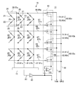
- FIG. 2 is an explanatory diagram showing a circuit configuration of the magnetic sensor device 10 to which the present invention is applied.
- the number of the magnetic sensors 20 is not limited as long as it is plural, but FIG. 2 shows a case where the number of the magnetic sensors 20 is nine. Illustrated.
- the plurality of magnetic sensors 20 are arranged in a matrix. However, as described with reference to FIG. 1, the plurality of magnetic sensors 20 are arranged in the conveyance direction A of the sheet-like medium 1. They are arranged in the intersecting direction B.
- the magnetic sensor 20a corresponds to the “first magnetic sensor” in the present invention
- the magnetic sensor 20d corresponds to the “second magnetic sensor” in the present invention
- the magnetic sensor 20b corresponds to the “third magnetic sensor” in the present invention
- the magnetic sensor 20e corresponds to the “fourth magnetic sensor” in the present invention.
- the power supply line 66a corresponds to the “first power supply line” in the present invention
- the power supply line 67a corresponds to the “second power supply line” in the present invention
- the power supply line 66b corresponds to the “third power supply line” in the present invention
- the power supply line 67b corresponds to the “fourth power supply line” in the present invention
- the output line 61a corresponds to a “first output line” in the present invention
- the output line 61b corresponds to a “second output line” in the present invention.
- the plurality of magnetic sensors 20 all have the same configuration, in FIG. 2, only the magnetic sensors 20a and 20b have a first magnetoresistive element 21, a second magnetoresistive element 22, Reference numerals of the point 25, the one end 28, and the other end 29 are given, and the other magnetic sensors 20 are omitted.
- a first magnetoresistive element 21 and a second magnetoresistive element 22 are electrically connected in series between one end 28 and the other end 29.
- a plurality of magnetic sensors 20 (magnetic sensors 20a, 20b,..., 20i) and a plurality of feeders electrically connected to one end 28 of the plurality of magnetic sensors 20 (magnetic sensors 20a, 20b,..., 20i) 66 (feed lines 66a, 66b, 66c), a plurality of feed lines 67 (feed lines 67a, 67b, 67c) electrically connected to the other ends 29 of the plurality of magnetic sensors 20, and a plurality of magnetic sensors 20 ( And a plurality of output lines 61 (output lines 61a, 61b, 61c) electrically connected to the midpoint 25 of the magnetic sensors 20a, 20b,.
- the power supply line 66a (first power supply line) is connected to one end 28 of the magnetic sensor 20a (first magnetic sensor), and the other end 29 of the magnetic sensor 20a is connected. Is connected to a power supply line 67a (second power supply line).
- the power supply line 66a is electrically connected to one end 28 of the magnetic sensor 20b (third magnetic sensor) and the magnetic sensor 20c, and the power supply line 67a is electrically connected to the other end 29 of the magnetic sensor 20b and the magnetic sensor 20c.
- a feeding line 66b (third feeding line) is connected to one end 28 of the magnetic sensor 20d (second magnetic sensor), and a feeding line 67b (fourth feeding line) is connected to the other end 29 of the magnetic sensor 20d. Yes.
- the feed line 66b is electrically connected to one end 28 of the magnetic sensor 20e (fourth magnetic sensor) and the magnetic sensor 20f, and the feed line 67b is electrically connected to the other end 29 of the magnetic sensor 20e and the magnetic sensor 20f.
- a power supply line 66c is connected to one end 28 of the magnetic sensors 20g, 20h, and 20i, and a power supply line 67c is connected to the other end 29 of the magnetic sensors 20g, 20h, and 20i.
- An output line 61a (first output line) is connected to the midpoint 25 of the magnetic sensors 20a, 20d, and 20g.
- An output line 61b (second output line) is connected to the midpoint 25 of the magnetic sensors 20b, 20e, and 20h.
- An output line 61c is connected to the midpoint 25 of the magnetic sensors 20c, 20f, and 20i.
- the power supply line 66 is a wiring for supplying the drive potential Vdd (first potential) supplied from the power supply line 68 to the magnetic sensor 20, and the power supply line 67 is a ground potential (second potential) supplied from the ground line 69. Wiring for supplying the potential) to the magnetic sensor 20.
- the drive potential Vdd is a positive constant potential
- the ground potential (second potential) is lower than the drive potential Vdd (first potential).
- the plurality of output lines 61 are connected to a selection circuit 70 formed of a multiplexer or the like. Further, a common output line 80 for outputting a signal to the amplifier circuit 120 shown in FIG. 1A extends from the selection circuit 70, and a buffer circuit 85 is inserted in the middle of the output line 80. .
- the magnetic sensor device 10 is provided with a switching circuit 90 that switches the potential applied to the power supply lines 66 and 67 based on the signal output from the sampling signal circuit 180 described with reference to FIG. ing.
- the switching circuit 90 includes a plurality of switches 91 (switches 91a, 91b, 91c) provided between the plurality of power supply lines 66 and the power supply line 68, and a plurality of power supply lines 67 and the ground line 69.
- a plurality of switch sections 93 (switch sections 93 a, 93 b, 93 c) including the provided switches 92 (switches 92 a, 92 b, 92 c) are provided.
- the switches 91, 92 perform opening / closing operations simultaneously.
- the switching circuit 90 includes a feedback amplifier 95 connected to the common output line 80, and the output line 96 of the feedback amplifier 95 has the same potential as the common output line 80.
- the switches 91 and 92 are connected to the magnetic sensor 20 (selected magnetic sensor 20) that outputs the detection result via the output line 61 among the plurality of magnetic sensors 20.
- the electric wires 66 and 67 are electrically connected to the power line 68 and the ground line 69, and the drive potential Vdd and the ground potential GND are applied to both ends (one end 28 and the other end 29) of the selected magnetic sensor 20.
- the switches 91 and 92 are electrically connected to the output line 96 of the feedback amplifier 95 for the power supply lines 66 and 67 connected to other magnetic sensors 20 that are not selected, and the power supply lines 66 and 67 are connected to the output line 96.
- the same potential as that of the common output line 80 is applied to both ends (one end 28 and the other end 29) of the magnetic sensor 20 that is not selected.
- the selected magnetic sensor 20 outputs the detection result from the midpoint 25 to the selection circuit 70 via the output line 61.
- the selection circuit 70 outputs the signal output via the output line 61 to the common output line 80 while shifting the time. Meanwhile, the potential of the midpoint 25 of the unselected magnetic sensor 20 is equal to the potential of the common output line 80.
- the potential of the common output line 80 (the potential of the output line 96) is the same as the potential of the output line 61 connected to the selected magnetic sensor 20 in each period.
- FIG. 3 is a timing chart showing the operation of the magnetic sensor device 10 to which the present invention is applied.
- FIGS. 3A, 3B, 3C, and 3D show potential changes in the feeder lines 66a and 67a.
- FIGS. 1 An explanatory diagram showing, an explanatory diagram showing a potential change of the feed lines 66b and 67b, an explanatory diagram showing a potential change of the feed lines 66c and 67c, and a potential change of the output lines 61 (61a, 61b, 61c), 80 and 96 It is explanatory drawing.
- the power supply line 66a and the power supply line 68 are made conductive by the switches 91a and 92a, and the power supply line 67a and the ground line 69 are connected.
- the drive potential Vdd is applied to the power supply line 66a
- the ground potential GND is applied to the power supply line 67a.
- the detection result (potential Va) of the magnetic sensor 20a, the detection result (potential Vb) of the magnetic sensor 20b, and the detection result (potential Vc) of the magnetic sensor 20c are sent to the common output line 80 via the selection circuit 70. Output in order.
- the switches 91b, 92b, 91c, and 92c make the power supply lines 66b, 67b, 66c, and 67c conductive with the output line 96.
- the potentials of the output lines 61a, 80, and 96 are at the potential Va, and thus the power supply lines 66b, 67b, and 66c. , 67c are at the potential Va.
- the potentials of the output lines 61b, 80, and 96 are the potential Vb, so that the power supply lines 66b, 67b, 66c, 67c is at the potential Vb.
- the potentials of the output lines 61c, 80, and 96 are the potential Vc. It has become.
- the switches 91b and 92b connect the power supply line 66b and the power supply line 68, connect the power supply line 67b and the ground line 69, and apply the drive potential Vdd to the power supply line 66b.
- a ground potential GND is applied to the electric wire 67b.
- the detection result (potential Vd) of the magnetic sensor 20d, the detection result (potential Ve) of the magnetic sensor 20e, and the detection result (potential Vf) of the magnetic sensor 20f are sent to the common output line 80 via the selection circuit 70. Output in order.
- the switches 91 a, 92 a, 91 c, and 92 c make the power supply lines 66 a, 67 a, 66 c, and 67 c conductive with the output line 96.
- the potentials of the output lines 61a, 80, and 96 are at the potential Vd, and thus the feeder lines 66a, 67a, and 66c. , 67c are at the potential Vd.
- the potentials of the output lines 61b, 80, and 96 are the potential Ve, so that the feeder lines 66a, 67a, 66c, 67c is at the potential Ve.
- the potentials of the output lines 61c, 80, and 96 are the potential Vf, so that the feeder lines 66a, 67a, 66c, and 67c are at the potential Vf. It has become.
- the switches 91c and 92c connect the power supply line 66c and the power supply line 68, connect the power supply line 67c and the ground line 69, and apply the drive potential Vdd to the power supply line 66c.
- a ground potential GND is applied to the electric wire 67c.
- the detection result (potential Vg) of the magnetic sensor 20g, the detection result (potential Vh) of the magnetic sensor 20h, and the detection result (potential Vi) of the magnetic sensor 20i are sent to the common output line 80 via the selection circuit 70. Output in order.
- the switches 91a, 92a, 91b, and 92b conduct the power supply lines 66a, 67a, 66b, and 67b to the output line 96.
- the potentials of the output lines 61a, 80, and 96 are the potential Vg, so that the feeder lines 66a, 67a, 66b, and 67b are at the potential Vg. It has become.
- the potentials of the output lines 61b, 80, and 96 are at the potential Vh, so that the feeder lines 66a, 67a, 66b, and 67b are at the potential Vh. ing.
- the potentials of the output lines 61c, 80, and 96 are the potential Vi, so that the power supply lines 66a, 67a, 66b, and 67b are at the potential Vf. It has become.
- the midpoints 25 of the plurality of magnetic sensors 20 are connected to the common output line 61, and the detection results of the plurality of magnetic sensors 20 are output via the common output line 61. Is done. For this reason, since the number of output lines 61 can be reduced, the configuration of the magnetic sensor device 10 can be simplified.
- the switching circuit 90 applies the drive potential Vdd and the ground potential GND to both ends of the magnetic sensor 20a when, for example, outputting the detection result from the midpoint 25 of the magnetic sensor 20a via the output line 61a.
- the power supply lines 66b, 67b, 66c, and 67c connected to the other magnetic sensors 20d and 20g having the midpoint 25 connected to the output line 61a are set to the same potential as the output line 61a. For this reason, the midpoint 25 of the other magnetic sensors 20d and 20g is the same as the potential of the midpoint 25 of the magnetic sensor 20a (the potential of the output line 61a). Therefore, the other magnetic sensors 20d and 20g are unlikely to affect the output of the detection result of the magnetic sensor 20a.
- the detection results of the magnetic sensors 20 a, 20 d, and 20 g can be properly output via the output line 61. . Even when the detection result is output from the other magnetic sensor 20, the potentials of the power supply lines 66 and 67 are similarly changed, so that the other magnetic sensor 20 hardly influences the output of the detection result of the magnetic sensor 20.
- the detection results output from the plurality of output lines 61 can be output via one common output line 80. For this reason, the circuit configuration of the magnetic sensor device 10 can be simplified.
- FIG. 4 is an explanatory diagram of another magnetic sensor device 10 to which the present invention is applied.
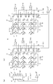
- FIGS. 4A and 4B are explanatory diagrams of a bridge circuit constituted by four magnetoresistive elements, and the bridge. It is explanatory drawing which shows the circuit structure of the magnetic sensor apparatus 10 provided with the circuit.
- a bridge in which the first magnetoresistive element 21 and the second magnetoresistive element 22 are connected in series between the one end 28 and the other end 29 is configured.
- the first magnetoresistive element 21 and the second magnetoresistive element 22 are connected in series between the one end 28 and the other end 29.
- another first magnetoresistive element 21 'and a second magnetoresistive element 22' are connected in series between one end 28 'and the other end 29'.
- the outputs from the midpoint 25 of the first magnetoresistive element 21 and the second magnetoresistive element 22 and from the midpoint 25 'of the first magnetoresistive element 21' and the second magnetoresistive element 22 ' are differential.
- the arithmetic circuit 16 composed of an amplifier and outputs from the midpoint 25 of the first magnetoresistive element 21 and the second magnetoresistive element 22, and the first magnetoresistive element 21 ′ and the second magnetoresistive element 22.
- a differential output out with respect to the output from the midpoint 25 ′ is output from the arithmetic circuit 16. For this reason, since the output signal is large, there is an advantage that the S / N ratio can be increased.
- the magnetic sensor device 10 has the two sensor circuits described with reference to FIG. 2 as shown in FIG. have.
- the two sensor circuits first sensor circuit and second sensor circuit
- one sensor circuit 15 first sensor circuit
- the other sensor circuit 15 ′ second sensor circuit
- the sensor circuit 15 includes a first magnetoresistive element 21 and a second magnetoresistive element 22 connected in series between one end 28 and the other end 29.
- a plurality of magnetic sensors 20 are provided.
- a power supply line 66 is electrically connected to one end 28 of the magnetic sensor 20, and a power supply line 67 is electrically connected to the other end 29 of the magnetic sensor 20.
- An output line 61a (first output line) is connected to the midpoint 25 of the magnetic sensors 20a, 20d, and 20g, and an output line 61b (second output line) is connected to the midpoint 25 of the magnetic sensors 20b, 20e, and 20h.
- the output line 61c is connected to the midpoint 25 of the magnetic sensors 20c, 20f, and 20i.
- the plurality of output lines 61 are connected to a selection circuit 70 composed of a multiplexer or the like.
- the sensor circuit 15 is provided with a switching circuit 90 that switches the potential applied to the power supply lines 66 and 67.
- the sensor circuit 15 ' includes a plurality of magnetic sensors 20' in which a first magnetoresistive element 21 'and a second magnetoresistive element 22' are connected in series between one end 28 'and the other end 29'.
- a power supply line 66 ′ is electrically connected to one end 28 ′ of the magnetic sensor 20 ′
- a power supply line 67 ′ is electrically connected to the other end 29 ′ of the magnetic sensor 20 ′.
- An output line 61a '(first output line) is connected to the midpoint 25' of the magnetic sensors 20a ', 20d' and 20g ', and an output line is connected to the midpoint 25' of the magnetic sensors 20b ', 20e' and 20h '.
- the 61b '(second output line) is connected, and an output line 61c' is connected to the midpoint 25 'of the magnetic sensors 20c', 20f ', 20i'.
- the plurality of output lines 61 ' are connected to a selection circuit 70' composed of a multiplexer or the like.
- the sensor circuit 15 ′ is provided with a switching circuit 90 ′ for switching the potential applied to the power supply lines 66 ′ and 67 ′.
- the switching circuits 90 and 90 'simultaneously select the magnetic sensors 20 and 20' for obtaining differential outputs in the two sensor circuits 15 and 15 '.
- the switching circuit 90 selects the magnetic sensor 20a (first magnetic sensor) of the sensor circuit 15
- the switching circuit 90 selects the magnetic sensor 20d (second magnetic sensor) of the sensor circuit 15
- the sheet-like medium identifying device 100 is illustrated as a detection device including the magnetic sensor device 10 in order to identify the type and authenticity of the sheet-like medium 1 (magnetic medium) such as banknotes and securities.
- the present invention may be applied to a magnetic sensor device 10 used for an encoder that detects the movement and position of a magnet (magnetic medium) that rotates or linearly moves in a state of facing the magnetic sensor 20 by a moving mechanism such as a motor. .
Landscapes
- Physics & Mathematics (AREA)
- General Physics & Mathematics (AREA)
- Condensed Matter Physics & Semiconductors (AREA)
- Measuring Magnetic Variables (AREA)
- Inspection Of Paper Currency And Valuable Securities (AREA)
Abstract
複数の磁気抵抗素子を直列に接続した複数の磁気センサの中点から検出結果を共通の出力線を介して適正に出力することのできる磁気センサ装置、および当該磁気センサ装置を備えた検出装置を提供すること。具体的には、磁気センサ装置10のセンサ回路15では、複数の磁気センサ20の第1磁気抵抗素子21と第2磁気抵抗素子22との中点25が共通の出力線61に接続されており、複数の磁気センサ20の検出結果は、共通の出力線61を介して出力される。切り換え回路90は、例えば、出力線61aを介して磁気センサ20aの中点25から出力線61aを介して検出結果を出力する際、磁気センサ20aの両端に駆動電位Vddおよびグランド電位GNDを印加するが、同一の出力線61aに中点25が接続された他の磁気センサ20d、20gに接続する給電線66b、67b、66c、67cを出力線61aと同一電位にする。
Description
本発明は、磁気抵抗素子を備えた磁気センサ装置、および検出装置に関するものである。
紙幣や有価証券等のシート状媒体では、偽造を防止するために磁気インク等を用いた印刷が施されている。かかるシート状媒体は、磁気抵抗素子を備えた磁気センサによって、所定の位置に磁気インク等によって印刷が施されているか否かを検出すれば、シート状媒体の真偽を判定することができる(例えば、特許文献1、2参照)。
シート状媒体全体から磁気インク等による印刷位置等を効率よく検出するには、磁気センサを複数用いる必要がある。その場合、複数の磁気センサの各々から出力線を引き回した構成では、回路構成が複雑になってしまい、磁気センサ装置のコストが増大する。従って、1本の出力線に複数の磁気センサを接続し、出力線から検出結果を時系列的に出力することが好ましい。しかしながら、2つの磁気抵抗素子を直列に接続した磁気センサの場合、その中点から検出結果を出力するため、選択された磁気センサでの検出結果を出力線を介して出力する際、非選択状態にある他の磁気センサでの検出結果が影響してしまうという問題点がある。
以上の問題点に鑑みて、本発明の課題は、複数の磁気抵抗素子を直列に接続した複数の磁気センサの中点から検出結果を共通の出力線を介して適正に出力することのできる磁気センサ装置、および当該磁気センサ装置を備えた検出装置を提供することにある。
上記課題を解決するために、本発明に係る磁気センサ装置は、一方端と他方端との間に第1磁気抵抗素子と第2磁気抵抗素子とが直列に電気的に接続された複数の磁気センサを備えたセンサ回路を有し、当該センサ回路が前記複数の磁気センサの検出結果を時系列的に出力する磁気センサ装置であって、前記複数の磁気センサには、少なくとも第1磁気センサおよび第2磁気センサが含まれており、前記センサ回路は、前記第1磁気センサの前記一方端に電気的に接続された第1給電線と、前記第1磁気センサの前記他方端に電気的に接続された第2給電線と、前記第2磁気センサの前記一方端に電気的に接続された第3給電線と、前記第2磁気センサの前記他方端に電気的に接続された第4給電線と、前記第1磁気センサの前記第1磁気抵抗素子と前記第2磁気抵抗素子との中点、および前記第2磁気センサの前記第1磁気抵抗素子と前記第2磁気抵抗素子との中点に接続された第1出力線と、前記第1給電線、前記第2給電線、前記第3給電線、および前記第4給電線の電位を切り換える切り換え回路と、を有し、前記切り換え回路は、前記第1出力線から前記第1磁気センサの検出結果を出力する第1期間では、前記第1給電線に第1電位を印加し、前記第2給電線に前記第1電位より低電位の第2電位を印加し、前記第3給電線および前記第4給電線を前記第1出力線と同一電位とし、前記第1出力線から前記第2磁気センサの検出結果を出力する第2期間では、前記第3給電線に前記第1電位を印加し、前記第4給電線に前記第2電位を印加し、前記第1給電線および前記第2給電線を前記第1出力線と同一電位とすることを特徴とする。
本発明における「給電線」「出力線」とは、電気的な経路を意味しており、その形態は、線状に限らず、平面状の導電パターンやブロック状の導電部材でなくてもよい。
本発明では、複数の磁気センサ(第1磁気センサおよび第2磁気センサ)の中点が共通の出力線(第1出力線)に接続されており、複数の磁気センサ(第1磁気センサおよび第2磁気センサ)の検出結果は、共通の出力線(第1出力線)を介して出力される。このため、出力線の数が少なく済むので、磁気センサ装置の構成を簡素化することができる。また、切り換え回路は、第1出力線を介して第1磁気センサの中点から検出結果を出力する際、第3給電線および第4給電線を第1出力線と同一電位にするため、第2磁気センサの中点は、第1磁気センサの中点の電位(第1出力線の電位)と同一となる。従って、第1磁気センサの検出結果の出力に第2磁気センサが影響を及ぼしにくい。また、切り換え回路は、第1出力線を介して第2磁気センサの中点から検出結果を出力する際、第1給電線および第2給電線を第1出力線と同一電位にするため、第1磁気センサの中点は、第2磁気センサの中点の電位(第1出力線の電位)と同一となる。従って、第2磁気センサの検出結果の出力に第1磁気センサが影響を及ぼしにくい。それ故、複数の磁気センサの検出結果を共通の出力線(第1出力線)を介して適正に出力することができる。
本発明において、前記複数の磁気センサは、さらに、第3磁気センサおよび第4磁気センサを含み、前記第1給電線は、前記第3磁気センサの前記一方端に電気的に接続され、前記第2給電線は、前記第3磁気センサの前記他方端に電気的に接続され、前記第3給電線は、前記第4磁気センサの前記一方端に電気的に接続され、前記第4給電線は、前記第2磁気センサの前記他方端に電気的に接続され、前記第3磁気センサの前記第1磁気抵抗素子と前記第2磁気抵抗素子との中点、および前記第4磁気センサの前記第1磁気抵抗素子と前記第2磁気抵抗素子との中点に接続された第2出力線を有し、前記切り換え回路は、前記第2出力線から前記第3磁気センサの検出結果を出力する第3期間では、前記第1給電線に前記第1電位を印加し、前記第2給電線に前記第2電位を印加し、前記第3給電線および前記第4給電線を前記第2出力線と同一電位とし、前記第2出力線から前記第4磁気センサの検出結果を出力する第4期間では、前記第3給電線に前記第1電位を印加し、前記第4給電線に前記第2電位を印加し、前記第1給電線および前記第2給電線を前記第2出力線と同一電位とすることが好ましい。かかる構成によれば、第3磁気センサの出力結果に第4磁気センサが影響を及ぼしにくく、第4磁気センサの出力結果に第3磁気センサが影響を及ぼしにくい。それ故、複数の磁気センサの検出結果を共通の出力線(第2出力線)を介して適正に出力することができる。
本発明において、前記センサ回路は、前記第1出力線および前記第2出力線に接続して当該第1出力線の電位および当該第2出力線の電位を選択して共通の出力線に出力する選択回路を備えていることが好ましい。かかる構成によれば、共通の出力線を介して第1磁気センサ、第2磁気センサ、第3磁気センサおよび第4磁気センサの検出結果を出力することができる。
本発明において、前記切り換え回路は、前記第1期間および前記第3期間では、前記第3給電線および前記第4給電線を前記共通出力線と同一電位とし、前記第2期間および前記第4期間では、前記第1給電線および前記第2給電線を前記共通出力線と同一電位とすることが好ましい。
本発明において、前記センサ回路として、第1センサ回路および第2センサ回路を有し、前記第1センサ回路の前記第1磁気センサと前記第2センサ回路の前記第1磁気センサとの差動出力、および前記第1センサ回路の前記第2磁気センサと前記第2センサ回路の前記第2磁気センサとの差動出力を算出する演算回路を有している構成を採用することができる。
本発明に係る磁気センサ装置は、例えば、シート状媒体識別装置やエンコーダ等、磁性媒体の種類または移動を検出する検出装置に用いることができる。この場合、検出装置は、磁性媒体と前記複数の磁気センサとを対向させた状態で当該複数の磁気センサに対して前記磁性媒体を該磁性媒体の面内方向に沿う方向に相対移動させる移動機構を有していることを特徴とする。
本発明では、複数の磁気センサ(第1磁気センサおよび第2磁気センサ)の中点が共通の出力線(第1出力線)に接続されており、複数の磁気センサ(第1磁気センサおよび第2磁気センサ)の検出結果は、共通の出力線(第1出力線)を介して出力される。このため、出力線の数が少なく済むので、磁気センサ装置の構成を簡素化することができる。また、切り換え回路は、第1出力線を介して第1磁気センサの中点から検出結果を出力する際、第3給電線および第4給電線を第1出力線と同一電位し、第1出力線を介して第2磁気センサの中点から検出結果を出力する際、第1給電線および第2給電線を第1出力線と同一電位にする。このため、複数の磁気センサの検出結果を共通の出力線(第1出力線)を介して適正に出力することができる。
以下、図面を参照して、本発明を適用した磁気センサ装置、および磁気センサ装置を備えたシート状媒体識別装置(検出装置)を説明する。
(シート状媒体識別装置の構成)
図1は、本発明を適用したシート状媒体識別装置の説明図であり、図1(a)、(b)は、シート状媒体識別装置全体のブロック図、およびシート状媒体識別装置に用いた磁気センサの説明図である。
図1は、本発明を適用したシート状媒体識別装置の説明図であり、図1(a)、(b)は、シート状媒体識別装置全体のブロック図、およびシート状媒体識別装置に用いた磁気センサの説明図である。
図1(a)において、シート状媒体識別装置100は、紙幣や有価証券等のシート状媒体1の種類や真偽を識別するための検出装置である。シート状媒体1は、所定位置に磁気インクによって印刷が施された磁性媒体である。シート状媒体識別装置100は、投入されたシート状媒体1を矢印Aで示す方向に搬送するベルトコンベア等の搬送機構110(移動機構)と、シート状媒体1の搬送経路においてシート状媒体1に対向する磁気センサ装置10を有している。本形態において、磁気センサ装置10は、シート状媒体1の搬送方向Aに交差する方向(矢印Bで示す方向)に延在するセンサヘッド11と、センサヘッド11を制御する制御部12とを有している。
センサヘッド11は、複数の磁気センサ20と、複数の磁気センサ20を保持するホルダ30と、複数の磁気センサ20に対してシート状媒体1とは反対側に設けられた磁石40と、磁石40および複数の磁気センサ20を覆うキャップ50とを有している。キャップ50は、ホルダ30と固定されている。本形態において、磁気センサ20は、センサヘッド11の延在方向(シート状媒体1の搬送方向Aに交差する方向B)に複数配置されている。制御部12は、回路基板121に実装された電子部品(図示せず)等によって構成されており、複数の磁気センサ20に対する給電や、複数の磁気センサ20での検出結果の出力を制御している。かかる構成のシート状媒体識別装置100において、搬送機構110(移動機構)は、シート状媒体1と磁気センサ装置10の磁気センサ20とを対向させたまま、シート状媒体1の面内方向に沿う方向にシート状媒体1と磁気センサ装置10の磁気センサ20とを相対移動させる。
シート状媒体識別装置100は、例えば、磁気センサ装置10の制御部12から磁気センサ20での検出結果が出力される増幅回路120と、増幅回路120から増幅された信号が出力されるサンプルホールド回路130と、サンプルホールド回路130から所定のタイミングで信号が出力されるA/D変換回路140とを有している。A/D変換回路140で生成されたデジタル信号は、マイクロコンピュータ150の判別回路160に出力される。マイクロコンピュータ150は、シート状媒体1の種類や真偽を判定するための判別データ等が格納された判別データ用メモリ170と、サンプリング信号回路180とを備えている。サンプルホールド回路130およびA/D変換回路140は、サンプリング信号回路180から出力された信号に基づいて、所定のタイミングで判別回路160に信号を出力する。
図1(b)に示すように、磁気センサ20では、一方端28と他方端29との間に第1磁気抵抗素子21と第2磁気抵抗素子22とが直列に接続されており、第1磁気抵抗素子21と第2磁気抵抗素子22との中点25から検出結果をアナログ信号として出力する。ここで、一方端28は、第1磁気抵抗素子21の第2磁気抵抗素子22とは反対側の端部からなり、他方端29は、第2磁気抵抗素子22の第1磁気抵抗素子21とは反対側の端部からなる。
(磁気センサ装置10の構成)
図2は、本発明を適用した磁気センサ装置10の回路構成を示す説明図である。なお、本発明に係る磁気センサ装置10において、磁気センサ20の数は複数であれば、その数は限定されることがないが、図2には、磁気センサ20の数が9個の場合を例示してある。また、図2では、複数の磁気センサ20がマトリクス状に配置されているが、図1を参照して説明したように、複数の磁気センサ20は、シート状媒体1の搬送方向Aに対して交差する方向Bに配列されている。
図2は、本発明を適用した磁気センサ装置10の回路構成を示す説明図である。なお、本発明に係る磁気センサ装置10において、磁気センサ20の数は複数であれば、その数は限定されることがないが、図2には、磁気センサ20の数が9個の場合を例示してある。また、図2では、複数の磁気センサ20がマトリクス状に配置されているが、図1を参照して説明したように、複数の磁気センサ20は、シート状媒体1の搬送方向Aに対して交差する方向Bに配列されている。
また、図2に示す複数の磁気センサ20のうち、例えば、磁気センサ20aが本発明における「第1磁気センサ」に相当し、磁気センサ20dが本発明における「第2磁気センサ」に相当し、磁気センサ20bが本発明における「第3磁気センサ」に相当し、磁気センサ20eが本発明における「第4磁気センサ」に相当する。また、複数の給電線66、67のうち、給電線66aが本発明における「第1給電線」に相当し、給電線67aが本発明における「第2給電線」に相当し、給電線66bが本発明における「第3給電線」に相当し、給電線67bが本発明における「第4給電線」に相当する。また、複数の出力線61のうち、出力線61aが本発明における「第1出力線」に相当し、出力線61bが本発明における「第2出力線」に相当する。また、複数の磁気センサ20はいずれも同一の構成を有していることから、図2では、磁気センサ20a、20bに対してのみ、第1磁気抵抗素子21、第2磁気抵抗素子22、中点25、一方端28、および他方端29の符号を付し、他の磁気センサ20については、これらの符号を省略する。
図2に示すように、磁気センサ装置10のセンサ回路15は、一方端28と他方端29との間に第1磁気抵抗素子21と第2磁気抵抗素子22とが直列に電気的に接続された複数の磁気センサ20(磁気センサ20a、20b・・、20i)と、複数の磁気センサ20(磁気センサ20a、20b・・、20i)の一方端28に電気的に接続された複数の給電線66(給電線66a、66b、66c)と、複数の磁気センサ20の他方端29に電気的に接続された複数の給電線67(給電線67a、67b、67c)と、複数の磁気センサ20(磁気センサ20a、20b・・、20i)の中点25に電気的に接続された複数の出力線61(出力線61a、61b、61c)とを有している。
より具体的には、複数の磁気センサ20のうち、磁気センサ20a(第1磁気センサ)の一方端28には給電線66a(第1給電線)が接続され、磁気センサ20aの他方端29には給電線67a(第2給電線)が接続されている。給電線66aは、磁気センサ20b(第3磁気センサ)および磁気センサ20cの一方端28に電気的に接続され、給電線67aは、磁気センサ20bおよび磁気センサ20cの他方端29に電気的に接続されている。
磁気センサ20d(第2磁気センサ)の一方端28には給電線66b(第3給電線)が接続され、磁気センサ20dの他方端29には給電線67b(第4給電線)が接続されている。給電線66bは、磁気センサ20e(第4磁気センサ)および磁気センサ20fの一方端28に電気的に接続され、給電線67bは、磁気センサ20eおよび磁気センサ20fの他方端29に電気的に接続されている。
磁気センサ20g、20h、20iの一方端28には給電線66cが接続され、磁気センサ20g、20h、20iの他方端29には給電線67cが接続されている。
磁気センサ20a、20d、20gの中点25には出力線61a(第1出力線)が接続されている。磁気センサ20b、20e、20hの中点25には出力線61b(第2出力線)が接続されている。磁気センサ20c、20f、20iの中点25には出力線61cが接続されている。
給電線66は、電源線68から供給された駆動電位Vdd(第1電位)を磁気センサ20に供給するための配線であり、給電線67は、グランド線69から供給されたグランド電位(第2電位)を磁気センサ20に供給するための配線である。ここで、駆動電位Vddは正の定電位であり、グランド電位(第2電位)は、駆動電位Vdd(第1電位)より低い電位である。
本形態の磁気センサ装置10において、複数の出力線61は、マルチプレクサ等からなる選択回路70に接続されている。また、選択回路70からは、図1(a)に示す増幅回路120に信号を出力する共通の出力線80が延在しており、出力線80の途中位置にバッファ回路85が挿入されている。
また、磁気センサ装置10には、図1(a)を参照して説明したサンプリング信号回路180から出力された信号に基づいて、給電線66、67に印加する電位を切り換える切り換え回路90が設けられている。
切り換え回路90は、複数の給電線66と電源線68との各間に設けられた複数のスイッチ91(スイッチ91a、91b、91c)と、複数の給電線67とグランド線69との各間に設けられたスイッチ92(スイッチ92a、92b、92c)とからなるスイッチ部93(スイッチ部93a、93b、93c)を複数、有している。複数のスイッチ部93(スイッチ部93a、93b、93c)の各々において、スイッチ91、92は、同時に開閉動作を行う。また、切り換え回路90は、共通の出力線80に接続されたフィードバックアンプ95を有しており、フィードバックアンプ95の出力線96は、共通の出力線80と同一電位となる。
このように構成した切り換え回路90において、スイッチ91、92は、複数の磁気センサ20のうち、出力線61を介して検出結果を出力する磁気センサ20(選択された磁気センサ20)に接続する給電線66、67については電源線68およびグランド線69に導通させ、選択された磁気センサ20の両端(一方端28および他方端29)に駆動電位Vddおよびグランド電位GNDを印加する。その際、スイッチ91、92は、選択されていない他の磁気センサ20に接続する給電線66、67については、フィードバックアンプ95の出力線96と導通させて給電線66、67を出力線96を介して短絡させ、選択されていない磁気センサ20の両端(一方端28および他方端29)に共通の出力線80と同一の電位を印加する。
従って、選択された磁気センサ20は、中点25から出力線61を介して選択回路70に検出結果を出力する。そして、選択回路70は、出力線61を介して出力された信号を時間をずらして共通の出力線80に出力する。その間、選択されていない磁気センサ20の中点25の電位は、共通の出力線80の電位と等しい。ここで、共通の出力線80の電位(出力線96の電位)は、各期間において、選択された磁気センサ20に接続する出力線61の電位と同一である。
(磁気センサ装置10の動作)
図3等を参照して、本発明を適用した磁気センサ装置10における動作を説明する。図3は、本発明を適用した磁気センサ装置10の動作を示すタイミングチャートであり、図3(a)、(b)、(c)、(d)は、給電線66a、67aの電位変化を示す説明図、給電線66b、67bの電位変化を示す説明図、給電線66c、67cの電位変化を示す説明図、および出力線61(61a、61b、61c)、80、96の電位変化を示す説明図である。なお、図3(a)、(b)、(c)において、給電線66a、66b、66cの電位変化を太い実線で示し、給電線67a、67b、67cの電位変化を太い破線で示してある。また、図3(a)、(b)、(c)において、給電線66、67の電位が同一となった場合でも、電位の変化が分かりやすいように、実線と破線とをわずかにずらしてある。
図3等を参照して、本発明を適用した磁気センサ装置10における動作を説明する。図3は、本発明を適用した磁気センサ装置10の動作を示すタイミングチャートであり、図3(a)、(b)、(c)、(d)は、給電線66a、67aの電位変化を示す説明図、給電線66b、67bの電位変化を示す説明図、給電線66c、67cの電位変化を示す説明図、および出力線61(61a、61b、61c)、80、96の電位変化を示す説明図である。なお、図3(a)、(b)、(c)において、給電線66a、66b、66cの電位変化を太い実線で示し、給電線67a、67b、67cの電位変化を太い破線で示してある。また、図3(a)、(b)、(c)において、給電線66、67の電位が同一となった場合でも、電位の変化が分かりやすいように、実線と破線とをわずかにずらしてある。
図2および図3に示すように、磁気センサ装置10においては、まず、切り換え回路90において、スイッチ91a、92aによって、給電線66aと電源線68とを導通させ、給電線67aとグランド線69とを導通させ、給電線66aに駆動電位Vddを印加し、給電線67aにグランド電位GNDを印加する。この状態で、磁気センサ20aの検出結果(電位Va)、磁気センサ20bの検出結果(電位Vb)、および磁気センサ20cの検出結果(電位Vc)を選択回路70を介して共通の出力線80に順に出力する。その間、スイッチ91b、92b、91c、92cは、給電線66b、67b、66c、67cを出力線96と導通させる。このため、磁気センサ20aの検出結果(電位Va)を出力する期間t1(第1期間)では、出力線61a、80、96の電位が電位Vaになっているので、給電線66b、67b、66c、67cは電位Vaになっている。また、磁気センサ20bの検出結果(電位Vb)を出力する期間t3(第3期間)では、出力線61b、80、96の電位が電位Vbになっているので、給電線66b、67b、66c、67cは電位Vbになっている。同様に、磁気センサ20cの検出結果(電位Vc)を出力する期間では、出力線61c、80、96の電位が電位Vcになっているので、給電線66b、67b、66c、67cは電位Vcになっている。
次に、切り換え回路90において、スイッチ91b、92bは、給電線66bと電源線68とを導通させ、給電線67bとグランド線69とを導通させ、給電線66bに駆動電位Vddを印加し、給電線67bにグランド電位GNDを印加する。この状態で、磁気センサ20dの検出結果(電位Vd)、磁気センサ20eの検出結果(電位Ve)、および磁気センサ20fの検出結果(電位Vf)を選択回路70を介して共通の出力線80に順に出力する。その間、スイッチ91a、92a、91c、92cは、給電線66a、67a、66c、67cを出力線96と導通させる。このため、磁気センサ20dの検出結果(電位Vd)を出力する期間t2(第2期間)では、出力線61a、80、96の電位が電位Vdになっているので、給電線66a、67a、66c、67cは電位Vdになっている。また、磁気センサ20eの検出結果(電位Ve)を出力する期間t4(第4期間)では、出力線61b、80、96の電位が電位Veになっているので、給電線66a、67a、66c、67cは電位Veになっている。同様に、磁気センサ20fの検出結果(電位Vf)を出力する期間では、出力線61c、80、96の電位が電位Vfになっているので、給電線66a、67a、66c、67cは電位Vfになっている。
次に、切り換え回路90において、スイッチ91c、92cは、給電線66cと電源線68とを導通させ、給電線67cとグランド線69とを導通させ、給電線66cに駆動電位Vddを印加し、給電線67cにグランド電位GNDを印加する。この状態で、磁気センサ20gの検出結果(電位Vg)、磁気センサ20hの検出結果(電位Vh)、および磁気センサ20iの検出結果(電位Vi)を選択回路70を介して共通の出力線80に順に出力する。その間、スイッチ91a、92a、91b、92bは、給電線66a、67a、66b、67bを出力線96と導通させる。このため、磁気センサ20gの検出結果(電位Vg)を出力する期間では、出力線61a、80、96の電位が電位Vgになっているので、給電線66a、67a、66b、67bは電位Vgになっている。また、磁気センサ20hの検出結果(電位Vh)を出力する期間では、出力線61b、80、96の電位が電位Vhになっているので、給電線66a、67a、66b、67bは電位Vhになっている。同様に、磁気センサ20iの検出結果(電位Vi)を出力する期間では、出力線61c、80、96の電位が電位Viになっているので、給電線66a、67a、66b、67bは電位Vfになっている。
(本形態の主な効果)
以上説明したように、本形態では、複数の磁気センサ20の中点25が共通の出力線61に接続されており、複数の磁気センサ20の検出結果は、共通の出力線61を介して出力される。このため、出力線61の数が少なく済むので、磁気センサ装置10の構成を簡素化することができる。
以上説明したように、本形態では、複数の磁気センサ20の中点25が共通の出力線61に接続されており、複数の磁気センサ20の検出結果は、共通の出力線61を介して出力される。このため、出力線61の数が少なく済むので、磁気センサ装置10の構成を簡素化することができる。
また、切り換え回路90は、例えば、磁気センサ20aの中点25から出力線61aを介して検出結果を出力する際、磁気センサ20aの両端に駆動電位Vddおよびグランド電位GNDを印加するが、同一の出力線61aに中点25が接続された他の磁気センサ20d、20gに接続する給電線66b、67b、66c、67cを出力線61aと同一電位にする。このため、他の磁気センサ20d、20gの中点25は、磁気センサ20aの中点25の電位(出力線61aの電位)と同一となる。従って、磁気センサ20aの検出結果の出力に他の磁気センサ20d、20gが影響を及ぼしにくい。従って、出力線61に複数の磁気センサ20a、20d、20gが電気的に接続されている場合でも、磁気センサ20a、20d、20gの検出結果を出力線61を介して適正に出力することができる。また、他の磁気センサ20から検出結果を出力する場合でも、給電線66、67の電位を同様に変化させるため、磁気センサ20の検出結果の出力に他の磁気センサ20が影響を及ぼしにくい。
また、本形態では、複数の出力線61を選択回路70に接続したため、複数の出力線61から出力される検出結果を1本の共通の出力線80を介して出力することができる。このため、磁気センサ装置10の回路構成を簡素化することができる。
(別の実施の形態)
図4は、本発明を適用した別の磁気センサ装置10の説明図であり、図4(a)、(b)は、4つの磁気抵抗素子によって構成されたブリッジ回路の説明図、および前記ブリッジ回路を備えた磁気センサ装置10の回路構成を示す説明図である。
図4は、本発明を適用した別の磁気センサ装置10の説明図であり、図4(a)、(b)は、4つの磁気抵抗素子によって構成されたブリッジ回路の説明図、および前記ブリッジ回路を備えた磁気センサ装置10の回路構成を示す説明図である。
上記実施の形態では、一方端28と他方端29との間に第1磁気抵抗素子21と第2磁気抵抗素子22とが直列に接続されたブリッジが構成されていた。これに対して、本形態では、図4(a)に示すように、一方端28と他方端29との間に第1磁気抵抗素子21と第2磁気抵抗素子22とが直列に接続されているとともに、一方端28′と他方端29′との間に別の第1磁気抵抗素子21′と第2磁気抵抗素子22′とが直列に接続されている。また、第1磁気抵抗素子21と第2磁気抵抗素子22との中点25、および第1磁気抵抗素子21′と第2磁気抵抗素子22′との中点25′からの出力は、差動増幅アンプからなる演算回路16に入力されており、第1磁気抵抗素子21と第2磁気抵抗素子22との中点25からの出力と、第1磁気抵抗素子21′と第2磁気抵抗素子22′との中点25′からの出力との差動出力outが演算回路16から出力される。このため、出力信号が大きいので、S/N比を大きくすることができる等の利点がある。
このような構成を採用した場合、磁気センサ装置10は、図4(b)に回路構成を示すように、図2を参照して説明したセンサ回路を2つ有しているとともに、演算回路16を有している。ここで、2つのセンサ回路(第1センサ回路および第2センサ回路)は、同一の構成を有していることから、一方のセンサ回路15(第1センサ回路)については、図2に示す各構成と同一の符号を付し、他方のセンサ回路15′(第2センサ回路)については、図2に示す各構成と同一の符号に「′」を付して、それらの説明を省略する。
図4(b)に示すように、磁気センサ装置10において、センサ回路15は、一方端28と他方端29との間に第1磁気抵抗素子21と第2磁気抵抗素子22とが直列に接続された複数の磁気センサ20を有している。磁気センサ20の一方端28には給電線66が電気的に接続され、磁気センサ20の他方端29には給電線67が電気的に接続されている。磁気センサ20a、20d、20gの中点25には出力線61a(第1出力線)が接続され、磁気センサ20b、20e、20hの中点25には出力線61b(第2出力線)が接続され、磁気センサ20c、20f、20iの中点25には出力線61cが接続されている。複数の出力線61は、マルチプレクサ等からなる選択回路70に接続されている。また、センサ回路15には、給電線66、67に印加する電位を切り換える切り換え回路90が設けられている。
また、センサ回路15′は、一方端28′と他方端29′との間に第1磁気抵抗素子21′と第2磁気抵抗素子22′とが直列に接続された複数の磁気センサ20′を有している。磁気センサ20′の一方端28′には給電線66′が電気的に接続され、磁気センサ20′の他方端29′には給電線67′が電気的に接続されている。磁気センサ20a′、20d′、20g′の中点25′には出力線61a′(第1出力線)が接続され、磁気センサ20b′、20e′、20h′の中点25′には出力線61b′(第2出力線)が接続され、磁気センサ20c′、20f′、20i′の中点25′には出力線61c′が接続されている。複数の出力線61′は、マルチプレクサ等からなる選択回路70′に接続されている。また、センサ回路15′には、給電線66′、67′に印加する電位を切り換える切り換え回路90′が設けられている。
ここで、切り換え回路90、90′は、2つのセンサ回路15、15′において差動出力を得るための磁気センサ20、20′を同時に選択する。例えば、切り換え回路90がセンサ回路15の磁気センサ20a(第1磁気センサ)を選択した際、切り換え回路90′は、センサ回路15の磁気センサ20a′(第1磁気センサ)を選択する。このため、演算回路16は、磁気センサ20a、20a′(第1磁気センサ)の差動出力outを算出し、出力する。また、切り換え回路90がセンサ回路15の磁気センサ20d(第2磁気センサ)を選択した際、切り換え回路90′は、センサ回路15の磁気センサ20d′(第2磁気センサ)を選択する。このため、演算回路16は、磁気センサ20d、20d′(第2磁気センサ)の差動出力outを算出し、出力する。
(他の実施の形態)
上記実施の形態では、選択されていない磁気センサ20に電気的に接続された給電線66、67の電位を出力線61と同一の電位にするにあたって、給電線66、67を電源線68およびグランド線69から切り離して出力線96と導通させたが、給電線66、67を電源線68およびグランド線69から切り離して給電線66、67同士を短絡させてもよい。この場合でも、選択されていない磁気センサ20の中点25が出力線61と同一の電位であるので、給電線66、67を出力線96と導通させなくても、給電線66、67の電位を出力線61と同一の電位とすることができる。
上記実施の形態では、選択されていない磁気センサ20に電気的に接続された給電線66、67の電位を出力線61と同一の電位にするにあたって、給電線66、67を電源線68およびグランド線69から切り離して出力線96と導通させたが、給電線66、67を電源線68およびグランド線69から切り離して給電線66、67同士を短絡させてもよい。この場合でも、選択されていない磁気センサ20の中点25が出力線61と同一の電位であるので、給電線66、67を出力線96と導通させなくても、給電線66、67の電位を出力線61と同一の電位とすることができる。
上記実施の形態では、磁気センサ装置10を備えた検出装置として、紙幣や有価証券等のシート状媒体1(磁性媒体)の種類や真偽を識別するためシート状媒体識別装置100を例示したが、モータ等の移動機構によって、磁気センサ20と対向した状態で回転移動や直線移動する磁石(磁性媒体)の移動や位置を検出するエンコーダに用いる磁気センサ装置10に本発明を適用してもよい。
1・・シート状媒体(磁性媒体)、10・・磁気センサ装置、11・・センサヘッド、12・・制御部、15、15′・・センサ回路、16・・演算回路、20、20′・・磁気センサ、20a、20a′・・磁気センサ(第1磁気センサ)、20b、20b′・・磁気センサ(第3磁気センサ)、20d、20d′・・磁気センサ(第2磁気センサ)、20e、20e′・・磁気センサ(第4磁気センサ)、21・・第1磁気抵抗素子、22・・第2磁気抵抗素子、25、25′・・中点、28、28′・・一方端、29、29′・・他方端、40・・磁石、61、61′、62、62′・・出力線、61a、61a′・・出力線(第1出力線)、61b、61b′・・出力線(第2出力線)、62a、62a′・・出力線(第3出力線)、62b、62b′・・出力線(第4出力線)、66、66′、67、67′・・給電線、66a、66a′・・給電線(第1給電線)、66b、66b′・・給電線(第3給電線)、67a、67a′・・給電線(第2給電線)、67b、67b′・・給電線(第4給電線)、68、68′・・駆動線、69、69′・・グランド線、70、70′・・選択回路、80、80′・・共通の出力線、90、90′・・切り換え回路、91、91′、92、92′・・スイッチ、95、95′・・フィードバックアンプ、96、96′・・フィーバックアンプの出力線、100・・シート状媒体識別装置(検出装置)、110・・搬送機構(移動機構)、120・・増幅回路、130・・サンプルホールド回路、140・・A/D変換回路、150・・マイクロコンピュータ、160・・判別回路、170・・判別データ用メモリ、180・・サンプリング信号回路、GND・・グランド電位、Vdd・・駆動電位
Claims (6)
- 一方端と他方端との間に第1磁気抵抗素子と第2磁気抵抗素子とが直列に電気的に接続された複数の磁気センサを備えたセンサ回路を有し、当該センサ回路が前記複数の磁気センサの検出結果を時系列的に出力する磁気センサ装置であって、
前記複数の磁気センサには、少なくとも第1磁気センサおよび第2磁気センサが含まれており、
前記センサ回路は、
前記第1磁気センサの前記一方端に電気的に接続された第1給電線と、
前記第1磁気センサの前記他方端に電気的に接続された第2給電線と、
前記第2磁気センサの前記一方端に電気的に接続された第3給電線と、
前記第2磁気センサの前記他方端に電気的に接続された第4給電線と、
前記第1磁気センサの前記第1磁気抵抗素子と前記第2磁気抵抗素子との中点、および前記第2磁気センサの前記第1磁気抵抗素子と前記第2磁気抵抗素子との中点に接続された第1出力線と、
前記第1給電線、前記第2給電線、前記第3給電線、および前記第4給電線の電位を切り換える切り換え回路と、
を有し、
前記切り換え回路は、
前記第1出力線から前記第1磁気センサの検出結果を出力する第1期間では、前記第1給電線に第1電位を印加し、前記第2給電線に前記第1電位より低電位の第2電位を印加し、前記第3給電線および前記第4給電線を前記第1出力線と同一電位とし、
前記第1出力線から前記第2磁気センサの検出結果を出力する第2期間では、前記第3給電線に前記第1電位を印加し、前記第4給電線に前記第2電位を印加し、前記第1給電線および前記第2給電線を前記第1出力線と同一電位とすることを特徴とする磁気センサ装置。 - 前記複数の磁気センサは、さらに、第3磁気センサおよび第4磁気センサを含み、
前記第1給電線は、前記第3磁気センサの前記一方端に電気的に接続され、
前記第2給電線は、前記第3磁気センサの前記他方端に電気的に接続され、
前記第3給電線は、前記第4磁気センサの前記一方端に電気的に接続され、
前記第4給電線は、前記第2磁気センサの前記他方端に電気的に接続され、
前記第3磁気センサの前記第1磁気抵抗素子と前記第2磁気抵抗素子との中点、および前記第4磁気センサの前記第1磁気抵抗素子と前記第2磁気抵抗素子との中点に接続された第2出力線を有し、
前記切り換え回路は、
前記第2出力線から前記第3磁気センサの検出結果を出力する第3期間では、前記第1給電線に前記第1電位を印加し、前記第2給電線に前記第2電位を印加し、前記第3給電線および前記第4給電線を前記第2出力線と同一電位とし、
前記第2出力線から前記第4磁気センサの検出結果を出力する第4期間では、前記第3給電線に前記第1電位を印加し、前記第4給電線に前記第2電位を印加し、前記第1給電線および前記第2給電線を前記第2出力線と同一電位とすることを特徴とする請求項1に記載の磁気センサ装置。 - 前記センサ回路は、前記第1出力線および前記第2出力線に接続して当該第1出力線の電位および当該第2出力線の電位を選択して共通の出力線に出力する選択回路を備えていることを特徴とする請求項2に記載の磁気センサ装置。
- 前記切り換え回路は、前記第1期間および前記第3期間では、前記第3給電線および前記第4給電線を前記共通出力線と同一電位とし、前記第2期間および前記第4期間では、前記第1給電線および前記第2給電線を前記共通出力線と同一電位とすることを特徴とする請求項3に記載の磁気センサ装置。
- 前記センサ回路として、第1センサ回路および第2センサ回路を有し、
前記第1センサ回路の前記第1磁気センサと前記第2センサ回路の前記第1磁気センサの差動出力、および前記第1センサ回路の前記第2磁気センサと前記第2センサ回路の前記第2磁気センサの差動出力を算出する演算回路を有していることを特徴とする請求項1乃至4の何れか一項に記載の磁気センサ装置。 - 請求項1乃至5の何れか一項に記載の磁気センサ装置を備え、磁性媒体の種類または移動を検出する検出装置であって、
前記磁性媒体と前記複数の磁気センサとを対向させた状態で当該複数の磁気センサに対して前記磁性媒体を該磁性媒体の面内方向に沿う方向に相対移動させる移動機構を有していることを特徴とする検出装置。
Applications Claiming Priority (2)
| Application Number | Priority Date | Filing Date | Title |
|---|---|---|---|
| JP2015-001765 | 2015-01-07 | ||
| JP2015001765A JP6456147B2 (ja) | 2015-01-07 | 2015-01-07 | 磁気センサ装置および検出装置 |
Publications (1)
| Publication Number | Publication Date |
|---|---|
| WO2016111114A1 true WO2016111114A1 (ja) | 2016-07-14 |
Family
ID=56355816
Family Applications (1)
| Application Number | Title | Priority Date | Filing Date |
|---|---|---|---|
| PCT/JP2015/084757 Ceased WO2016111114A1 (ja) | 2015-01-07 | 2015-12-11 | 磁気センサ装置および検出装置 |
Country Status (2)
| Country | Link |
|---|---|
| JP (1) | JP6456147B2 (ja) |
| WO (1) | WO2016111114A1 (ja) |
Families Citing this family (1)
| Publication number | Priority date | Publication date | Assignee | Title |
|---|---|---|---|---|
| CN107993332A (zh) * | 2017-12-07 | 2018-05-04 | 威海华菱光电股份有限公司 | 磁图像传感器 |
Citations (2)
| Publication number | Priority date | Publication date | Assignee | Title |
|---|---|---|---|---|
| JPH01254880A (ja) * | 1988-04-04 | 1989-10-11 | Sharp Corp | 磁気パターン検出装置 |
| JP2012047685A (ja) * | 2010-08-30 | 2012-03-08 | Mitsubishi Electric Corp | 磁気センサ装置及びそれを用いた読み取り判別装置 |
Family Cites Families (4)
| Publication number | Priority date | Publication date | Assignee | Title |
|---|---|---|---|---|
| JPH08145718A (ja) * | 1994-11-17 | 1996-06-07 | Canon Electron Inc | 磁気抵抗効果センサ |
| EP2071350B1 (en) * | 2006-08-31 | 2015-03-25 | Alps Electric Co., Ltd. | Magnetism detecting apparatus |
| US8952686B2 (en) * | 2011-10-25 | 2015-02-10 | Honeywell International Inc. | High current range magnetoresistive-based current sensor |
| JP2014095656A (ja) * | 2012-11-12 | 2014-05-22 | Nidec Sankyo Corp | 磁気センサ装置 |
-
2015
- 2015-01-07 JP JP2015001765A patent/JP6456147B2/ja active Active
- 2015-12-11 WO PCT/JP2015/084757 patent/WO2016111114A1/ja not_active Ceased
Patent Citations (2)
| Publication number | Priority date | Publication date | Assignee | Title |
|---|---|---|---|---|
| JPH01254880A (ja) * | 1988-04-04 | 1989-10-11 | Sharp Corp | 磁気パターン検出装置 |
| JP2012047685A (ja) * | 2010-08-30 | 2012-03-08 | Mitsubishi Electric Corp | 磁気センサ装置及びそれを用いた読み取り判別装置 |
Also Published As
| Publication number | Publication date |
|---|---|
| JP6456147B2 (ja) | 2019-01-23 |
| JP2016125967A (ja) | 2016-07-11 |
Similar Documents
| Publication | Publication Date | Title |
|---|---|---|
| JP6548868B2 (ja) | 磁気検査装置、および紙葉類処理装置 | |
| US9396366B2 (en) | Magnetic sensor device | |
| JP6564528B2 (ja) | 磁気イメージセンサー | |
| SE529125C2 (sv) | Sätt och anordning för att bestämma läget hos ett förpackningsmaterial med magnetiska markeringar | |
| JP2010060341A (ja) | 磁気センサ | |
| JP4798191B2 (ja) | 磁気センサ装置 | |
| CN103728573B (zh) | 磁场检测装置和磁场检测方法 | |
| US10775470B2 (en) | Magnetic detection apparatus | |
| JP6456147B2 (ja) | 磁気センサ装置および検出装置 | |
| JP6454228B2 (ja) | 磁気センサ装置 | |
| US7615993B2 (en) | Magnetic line-type position-angle detecting device | |
| US8125217B2 (en) | Magnetoresistive array design for improved sensor-to-magnet carrier tolerances | |
| JP5999550B2 (ja) | 不揮発性メモリを用いた調整回路及びこれを備えた物理量センサ | |
| CN205302449U (zh) | 磁图像传感器 | |
| CN111795638B (zh) | 总线兼容的传感器元件和通信系统 | |
| JP2021505999A (ja) | 磁気イメージセンサー | |
| KR100676212B1 (ko) | 홀 센서 구동회로 및 그 구동회로에 의한 포인팅 장치 | |
| JP2016115240A (ja) | 乗算回路及びそれを備えた電力センサー | |
| JP5612782B1 (ja) | 磁気検出デバイス、磁気センサ及び紙幣鑑別装置 | |
| JP4771015B2 (ja) | 磁気センサ | |
| JP2016057125A (ja) | 磁気ラインセンサ及びこの磁気ラインセンサを用いた画像化装置 | |
| JP2017194455A (ja) | 磁気識別装置 |
Legal Events
| Date | Code | Title | Description |
|---|---|---|---|
| 121 | Ep: the epo has been informed by wipo that ep was designated in this application |
Ref document number: 15876987 Country of ref document: EP Kind code of ref document: A1 |
|
| NENP | Non-entry into the national phase |
Ref country code: DE |
|
| 122 | Ep: pct application non-entry in european phase |
Ref document number: 15876987 Country of ref document: EP Kind code of ref document: A1 |