WO2016110896A1 - 発光素子及び発光素子の製造方法 - Google Patents
発光素子及び発光素子の製造方法 Download PDFInfo
- Publication number
- WO2016110896A1 WO2016110896A1 PCT/JP2015/006121 JP2015006121W WO2016110896A1 WO 2016110896 A1 WO2016110896 A1 WO 2016110896A1 JP 2015006121 W JP2015006121 W JP 2015006121W WO 2016110896 A1 WO2016110896 A1 WO 2016110896A1
- Authority
- WO
- WIPO (PCT)
- Prior art keywords
- layer
- semiconductor layer
- acid
- light emitting
- light
- Prior art date
- Legal status (The legal status is an assumption and is not a legal conclusion. Google has not performed a legal analysis and makes no representation as to the accuracy of the status listed.)
- Ceased
Links
Images



Classifications
-
- H—ELECTRICITY
- H10—SEMICONDUCTOR DEVICES; ELECTRIC SOLID-STATE DEVICES NOT OTHERWISE PROVIDED FOR
- H10H—INORGANIC LIGHT-EMITTING SEMICONDUCTOR DEVICES HAVING POTENTIAL BARRIERS
- H10H20/00—Individual inorganic light-emitting semiconductor devices having potential barriers, e.g. light-emitting diodes [LED]
- H10H20/80—Constructional details
- H10H20/81—Bodies
- H10H20/819—Bodies characterised by their shape, e.g. curved or truncated substrates
- H10H20/82—Roughened surfaces, e.g. at the interface between epitaxial layers
-
- H—ELECTRICITY
- H10—SEMICONDUCTOR DEVICES; ELECTRIC SOLID-STATE DEVICES NOT OTHERWISE PROVIDED FOR
- H10H—INORGANIC LIGHT-EMITTING SEMICONDUCTOR DEVICES HAVING POTENTIAL BARRIERS
- H10H20/00—Individual inorganic light-emitting semiconductor devices having potential barriers, e.g. light-emitting diodes [LED]
- H10H20/80—Constructional details
- H10H20/81—Bodies
- H10H20/822—Materials of the light-emitting regions
- H10H20/824—Materials of the light-emitting regions comprising only Group III-V materials, e.g. GaP
-
- H—ELECTRICITY
- H10—SEMICONDUCTOR DEVICES; ELECTRIC SOLID-STATE DEVICES NOT OTHERWISE PROVIDED FOR
- H10H—INORGANIC LIGHT-EMITTING SEMICONDUCTOR DEVICES HAVING POTENTIAL BARRIERS
- H10H20/00—Individual inorganic light-emitting semiconductor devices having potential barriers, e.g. light-emitting diodes [LED]
- H10H20/80—Constructional details
- H10H20/84—Coatings, e.g. passivation layers or antireflective coatings
-
- H—ELECTRICITY
- H10—SEMICONDUCTOR DEVICES; ELECTRIC SOLID-STATE DEVICES NOT OTHERWISE PROVIDED FOR
- H10P—GENERIC PROCESSES OR APPARATUS FOR THE MANUFACTURE OR TREATMENT OF DEVICES COVERED BY CLASS H10
- H10P50/00—Etching of wafers, substrates or parts of devices
-
- H—ELECTRICITY
- H10—SEMICONDUCTOR DEVICES; ELECTRIC SOLID-STATE DEVICES NOT OTHERWISE PROVIDED FOR
- H10P—GENERIC PROCESSES OR APPARATUS FOR THE MANUFACTURE OR TREATMENT OF DEVICES COVERED BY CLASS H10
- H10P50/00—Etching of wafers, substrates or parts of devices
- H10P50/60—Wet etching
- H10P50/64—Wet etching of semiconductor materials
- H10P50/642—Chemical etching
Definitions
- the present invention relates to a light-emitting element and a method for manufacturing the light-emitting element, and in particular, a first semiconductor layer, an active layer, a second semiconductor layer, and a window layer / support substrate are formed on a substrate by epitaxial growth.
- the present invention relates to a structure and a manufacturing method when a roughening treatment is performed on a formed light emitting element substrate.
- LEDs light emitting diodes
- Most conventional lighting fixtures are a combination of an InGaN blue LED and a fluorescent agent.
- a fluorescent agent when used, the occurrence of Stokes loss is unavoidable in principle, and there is a problem that it is impossible to convert all the light received by the fluorescent agent into another wavelength. In particular, this problem is remarkable in a region such as yellow or red having a longer wavelength than blue.
- InGaN-based LEDs which are blue LEDs, generally use a sapphire substrate, and the sapphire substrate is transparent with respect to the emission wavelength, and thus has an ideal form for the above-described lighting fixture.
- GaAs or Ge serving as a light-absorbing substrate with respect to the emission wavelength is used as a starting substrate, which is not suitable for the above-described use.
- a window layer is grown to a thickness that can be used for a support substrate as shown in Patent Document 1 or a method of bonding a transparent substrate to a light emitting portion as shown in Patent Document 2, and absorbs light.
- a technique for removing a starting substrate, which is a substrate, to make an LED is disclosed.
- the substrate used for bonding has a thickness of 200 ⁇ m or more.
- the film thickness required for the LED element is at most about 100 ⁇ m in consideration of the light distribution characteristic and the assemblability with other elements. Therefore, it is necessary to thin the film to such a thickness. In thinning processing, the number of man-hours due to processing and the risk of wafer breakage also increase, leading to increased costs and reduced yield.
- the window layer may be grown to a desired thickness. Since the step of bonding and bonding the substrates is not necessary, it can be formed at a low cost and is an excellent method.
- the window layer / current diffusion layer and the window layer / support substrate are roughened, and the light emitting portion is rough.
- a method that does not face the surface has been proposed.
- this method requires the formation of a deep trench that penetrates the window / current diffusion layer portion, which is not only costly, but the height difference between the upper and lower electrodes is too large, so that wire bonding can be performed. difficult.
- Even when applied to the flip chip type it is necessary to form a thick insulating film and a very long metal via, which causes an increase in cost. Therefore, it is desirable that the window layer / current diffusion layer portion which is the upper electrode portion is thin.
- Patent Documents 4 and 5 are disclosed as disclosure techniques in which the window layer / current diffusion layer is thin, the height difference between the upper electrode part and the lower electrode part is small, and the light extraction part or the light reflection part has a rough surface. It is done.
- a rough surface is formed on the surface of the n-type semiconductor layer on the side opposite to the light extraction surface side, but this is a technical disclosure of a flip-chip type, and efficient light from the electrode side to the window layer side.
- the purpose is reflection. Further, it is disclosed that it is difficult to apply a rough surface to both the window layer / support substrate and the light emitting portion.
- Patent Document 5 discloses a technique for performing a roughening treatment on the surface of an AlGaInP-based clad layer.
- a clad layer is made of (Al 0.5 Ga 0.5 ) 0.5 In 0.5.
- a technique for laminating a window layer made of (Al x Ga 1-x ) 0.5 In 0.5 P (0.5 ⁇ x) on the upper part of the cladding layer is disclosed. That is, a technique relating to the fact that the layer to be roughened is a layer having an Al composition higher than that of the cladding layer is disclosed.
- the Al content ratio is The higher the value, the higher the etching rate, and the more difficult it is to apply a rough surface. For this reason, in order to obtain a desired rough surface, it is necessary to increase the etching depth. As a result, the etching is larger than the pad electrode formation surface and excessively etched, so that the mechanical strength of the pad electrode portion is lowered. As a result, there is a problem that the risk of chip cracking during wire bonding increases.
- the Al content of the cladding layer is increased.
- the etching depth increases in order to obtain a desired rough surface, and accordingly, the thickness of the cladding layer is set to the carrier confinement function. It is also necessary to make it much thicker than the minimum necessary thickness.
- the present invention has been made in view of the above problems, and has a window layer / support substrate and a light emitting part, and a clad layer is formed when a rough surface is formed on the surface of the light emitting part with a rough surface liquid (etching liquid).
- An object of the present invention is to provide a light emitting device that suppresses the occurrence of chip cracking at the time of wire bonding by suppressing the etching depth necessary to obtain a desired rough surface shape while maintaining the carrier confinement effect.
- a window layer / support substrate a second conductivity type second semiconductor layer, an active layer, and a first conductivity layer provided on the window layer / support substrate.
- a first ohmic electrode is provided on the first semiconductor layer, and at least a part of a surface of the first semiconductor layer and a side surface of the light emitting portion is covered with an insulating protective film, and the surface of the first semiconductor layer and the window The surface of the layer / support substrate is roughened,
- the first semiconductor layer has a structure of at least two layers, and the layer on the side subjected to the roughening treatment is made of a material having a smaller Al composition than the layer on the active layer side.
- a light emitting element is provided.
- the etching depth required to obtain the desired rough surface shape is suppressed, and light emission that suppresses chip cracking during wire bonding is suppressed. It can be set as an element.
- the layer on the side subjected to the roughening treatment of the first semiconductor layer (Al x Ga 1-x ) y In 1-y P (0 ⁇ x ⁇ 0.6, 0.4 ⁇ y ⁇ 0.6) or Al z Ga 1-z As (0 ⁇ z ⁇ 0.3) Consists of
- the layer on the active layer side of the first semiconductor layer is (Al x Ga 1-x ) y In 1-y P (0.6 ⁇ x ⁇ 1, 0.4 ⁇ y ⁇ 0.6) or Al z Ga 1-z As (0.3 ⁇ z ⁇ 1) It is preferable that it consists of. If it is such, while maintaining the carrier confinement effect of the clad layer, the etching depth necessary to obtain the desired rough surface shape is suppressed, and the light emitting element that suppresses the occurrence of chip cracking during wire bonding It can be surely.
- a step of forming a light emitting portion by sequentially growing a first semiconductor layer, an active layer, and a second semiconductor layer on a substrate with a lattice-matching material with the substrate, and the light emission Forming a window layer and supporting substrate by epitaxial growth on the substrate with a material of a non-lattice matching system with respect to the substrate, removing the substrate, and forming a first ohmic electrode on the first semiconductor layer
- An element isolation step a step of forming a second ohmic electrode on the window layer / support substrate from which the light emitting portion has been removed, and at least a part of the first semiconductor layer surface and the side surface of the light emitting portion with an insulating protective film Coating step and the window layer / support substrate Made from the second surface roughening treatment step to roughen the surface and side,
- the first semiconductor layer is formed of a material having a structure having at least two layers, and the layer on the side subjected to the roughening treatment is made of a material having a smaller Al composition than the layer on the active layer side.
- Provided is a method for manufacturing a light emitting device.
- the layer on the side subjected to the roughening treatment of the first semiconductor layer (Al x Ga 1-x ) y In 1-y P (0 ⁇ x ⁇ 0.6, 0.4 ⁇ y ⁇ 0.6) or Al z Ga 1-z As (0 ⁇ z ⁇ 0.3) age, A layer on the active layer side of the first semiconductor layer, (Al x Ga 1-x ) y In 1-y P (0.6 ⁇ x ⁇ 1, 0.4 ⁇ y ⁇ 0.6) or Al z Ga 1-z As (0.3 ⁇ z ⁇ 1) It is preferable that If it is such, while maintaining the carrier confinement effect of the clad layer, the etching depth necessary to obtain the desired rough surface shape is suppressed, and the light emitting element that suppresses the occurrence of chip cracking during wire bonding Can be reliably manufactured.
- the first roughening treatment step A mixed solution of an organic acid and an inorganic acid is used, and the organic acid contains at least one of citric acid, malonic acid, formic acid, acetic acid, and tartaric acid, and the inorganic acid includes hydrochloric acid, sulfuric acid, nitric acid, and hydrofluoric acid.
- the second roughening treatment step includes A mixed solution containing an organic acid and an inorganic acid is used, and the organic acid includes at least one of citric acid, malonic acid, formic acid, acetic acid, and tartaric acid, and the inorganic acid includes hydrochloric acid, sulfuric acid, nitric acid, It is preferable to use a solution containing at least one of hydrofluoric acid and containing iodine.
- the etching depth necessary for obtaining a desired rough surface shape is suppressed, and a light emitting device that suppresses chip cracking during wire bonding is realized. it can. Further, in the light emitting device manufacturing method of the present invention, while maintaining the carrier confinement effect of the clad layer, the etching depth necessary for obtaining a desired rough surface shape is suppressed, and chip cracking occurs during wire bonding. A suppressed light-emitting element can be manufactured.
- the first semiconductor layer is composed of layers having two or more types of Al composition, and the first semiconductor layer is subjected to the roughening treatment.
- the material is a material having a lower Al composition than the material of the active layer side, the mechanical strength of the pad electrode part is reduced by excessive etching while maintaining the carrier confinement effect of the cladding layer, and chip cracking occurs during wire bonding. It has been conceived that a rough surface having the required unevenness can be obtained by suppressing the occurrence of the above. And the best form for implementing these was scrutinized and the present invention was completed.
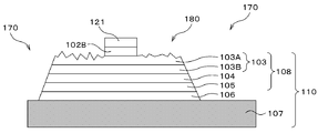
- the light-emitting element of the present invention will be described with reference to FIG.
- the light emitting device 1 of the present invention is provided on a window layer / support substrate 107, a window layer / support substrate 107, a second conductivity type second semiconductor layer 105, an active layer 104,
- the light emitting unit 108 includes the first conductivity type first semiconductor layer 103 in this order.
- a first ohmic electrode 121 is provided on the first semiconductor layer 103. Further, at least a part of the surface of the first semiconductor layer 103 and the side surface of the light emitting unit 108 is covered with an insulating protective film 150, and the surface of the first semiconductor layer 103 and the surface and side surfaces of the window layer / support substrate 107 are roughened. It has been done. As shown in FIG. 1, the first ohmic electrode 121 may be provided on the first semiconductor layer 103 via the first selective etching layer 102B.
- the first semiconductor layer 103 has a structure of at least two layers.
- the layer subjected to the roughening treatment (hereinafter referred to as the low Al composition layer 103A) is made of a material having a smaller Al composition than the layer on the active layer side (hereinafter referred to as the high Al composition layer 103B). Is.
- the low Al composition layer 103A includes (Al x Ga 1-x ) y In 1-y P (0 ⁇ x ⁇ 0.6, 0.4 ⁇ y ⁇ 0.6) or Al z Ga 1 -Z As (0 ⁇ z ⁇ 0.3), and the high Al composition layer 103B has (Al x Ga 1-x ) y In 1-y P (0.6 ⁇ x ⁇ 1, 0.4 ⁇ y ⁇ 0.6) or Al z Ga 1-z As (0.3 ⁇ z ⁇ 1).
- the light emitting element 1 is formed with a removed portion 170 from which at least the first semiconductor layer 103 and the active layer 104 of the light emitting portion 108 are removed, and a non-removed portion 180 other than the removed portion 170. Note that when the active layer 104 is removed, the surface of the removed portion 170 becomes the second semiconductor layer 105, and when the removed portion 170 is removed, the surface of the removed portion 170 becomes the window layer / supporting substrate 107.
- the present invention works particularly effectively.
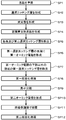
- a substrate 101 is prepared as a starting substrate (SP1 in FIG. 2).
- GaAs or Ge can be preferably used as the substrate 101.
- the material of the active layer 104 to be described later can be epitaxially grown in a lattice matching system, the quality of the active layer 104 can be easily improved, and the luminance can be increased and the life characteristics can be improved.
- a selective etching layer 102 may be formed on the substrate 101 (SP2 in FIG. 2).
- the selective etching layer 102 can be formed on the substrate 101 by, for example, MOVPE (metal organic chemical vapor deposition), MBE (molecular beam epitaxy), or CBE (chemical beam epitaxy).
- the selective etching layer 102 has a layer structure of two or more layers, and preferably includes at least a second selective etching layer 102A in contact with the substrate 101 and a first selective etching layer 102B in contact with a first semiconductor layer 103 described later.
- the second selective etching layer 102A and the first selective etching layer 102B may be made of different materials or compositions.
- the substrate 101 and the first conductivity type first semiconductor layer 103 of the lattice matching system, the active layer 104, and the second conductivity type second semiconductor layer 105 are sequentially grown by epitaxial growth to form the light emitting portion 108 (FIG. 2 SP3).
- a window layer / supporting substrate 107 is formed by epitaxial growth on the light-emitting portion 108 with a non-lattice matching material with respect to the substrate 101 to produce an epitaxial substrate 109 (SP4 in FIG. 2).
- an epitaxial substrate 109 can be produced by epitaxially growing the buffer layer 106 and the window layer / supporting substrate 107 in this order.
- the window layer / support substrate 107 may be formed by HVPE (hydride vapor phase epitaxy).
- the active layer 104 has (Al x Ga 1-x ) y In 1-y P (0 ⁇ x ⁇ 1, 0.4 ⁇ y ⁇ 0.6) or Al z Ga 1-z As (0 ⁇ z ⁇ 0.45).
- AlGaInP when applied to visible light illumination, it is preferable to select AlGaInP, and when applied to infrared illumination, it is preferable to select AlGaAs.
- the design of the active layer 104 is not limited to the above materials because the wavelength can be adjusted by using a superlattice or the like other than the wavelength resulting from the material composition.
- AlGaInP or AlGaAs is selected for the first semiconductor layer 103 and the second semiconductor layer 105, and the selection is not necessarily the same material system as that of the active layer 104.
- the first semiconductor layer 103, the active layer 104, and the second semiconductor layer 105 having the simplest structure are exemplified by AlGaInP, which is the same material, but the first semiconductor layer 103 or the second semiconductor layer is exemplified.
- each layer includes a plurality of layers, and it is needless to say that the first semiconductor layer 103 or the second semiconductor layer 105 is not limited to a single layer.
- the first semiconductor layer 103 has a structure of two or more layers.
- the low Al composition layer 103A on the side of the first semiconductor layer 103 on which the roughening treatment is performed is formed of a material having a lower Al composition than the high Al composition layer 103B on the active layer side.
- the high Al composition layer 103B is a functional layer having a function of a clad layer, and is not limited to a single composition or a single condition layer.
- the low Al composition layer 103A is made of (Al x Ga 1-x ) y In 1-y P (0 ⁇ x ⁇ 0.6, 0.4 ⁇ y ⁇ 0.6) or Al z Ga 1 ⁇ z As (0 ⁇ z ⁇ 0.3)
- the high Al composition layer 103B is made of (Al x Ga 1-x ) y In 1-y P (0.6 ⁇ x ⁇ 1, 0.4 ⁇ y ⁇ 0.6) or Al z Ga 1-z As (0.3 ⁇ z ⁇ 1).
- the window layer / supporting substrate 107 GaP, GaAsP, AlGaAs, sapphire (Al 2 O 3 ), quartz (SiO 2 ), SiC, or the like can be suitably used.
- the buffer layer 106 is most preferably formed of GaInP, but any material can be selected for the buffer layer 106 as long as it has a buffer function. Needless to say, this is not limitative. Further, when GaAsP is selected as the window layer / supporting substrate 107, the weather resistance is good.
- the epitaxial substrate 109 has a large warp.
- the light emitting portion 108 is preferably grown with a crystallographic inclination of 12 degrees or more with respect to the growth surface.
- This tilt direction can be selected in any direction, but when adopting the process of separating the elements in the scribe and braking process, select the direction in which the crystal axis does not tilt and is orthogonal to one of the scribe lines, If the direction in which the crystal axis is inclined is selected for the other of the scribe lines, it is possible to reduce the number of elements whose side surfaces are inclined with respect to the element surface and the back surface.
- a direction in which one of the scribe lines is not inclined is usually selected, but the inclination of the element side surface of about 20 degrees is not a big problem on the assembly. Therefore, the orthogonal directions do not have to coincide exactly, and an angular range of about ⁇ 20 degrees from the orthogonal directions is conceptually included in the orthogonal directions.
- the substrate 101 and the second selective etching layer 102A are removed from the epitaxial substrate 109, and only the first selective etching layer 102B remains on the surface of the first semiconductor layer 103 of the light emitting element substrate 110 as shown in FIG. (SP5 in FIG. 2).
- the first selective etching layer 102 ⁇ / b> B remains on the surface of the first semiconductor layer 103 by removing the substrate 101 by wet etching using the second selective etching layer 102 ⁇ / b> A from the epitaxial substrate 109. it can.
- a first ohmic electrode 121 for supplying a potential to the light emitting element is formed on the surface of the first selective etching layer 102B on the first semiconductor layer 103 (SP6 in FIG. 2). .
- the first selective etching layer 102B in a region other than the lower portion of the first ohmic electrode 121 is removed (SP7 in FIG. 2).
- the first selective etching layer 102B in a region other than the lower portion of the first ohmic electrode 121 can be removed by etching.
- a first roughening treatment step is performed in which the surface of the first semiconductor layer 103 is roughened (SP8 in FIG. 2).
- a mixed solution of an organic acid and an inorganic acid is used, and the organic acid contains a carboxylic acid, particularly one or more of citric acid, malonic acid, formic acid, acetic acid, and tartaric acid.
- the inorganic acid can be prepared using a solution containing one or more of hydrochloric acid, sulfuric acid, nitric acid, and hydrofluoric acid. In this way, the surface can be reliably roughened.
- the first rough surface liquid mainly performs the first roughening treatment on the low Al composition layer 103A.
- the low Al composition layer 103A and the high Al composition layer 103B are formed of the same material, for example, both of them are AlGaInP-based materials, the high Al composition layer 103B is etched faster than the low Al composition layer 103A.
- the thickness of the low Al composition layer 103A is preferably thicker than the planned etching width.
- the low Al composition layer 103A may be formed thinner than the planned etching width. preferable.
- the size of the unevenness on the rough surface can be determined by the Al content of the low Al composition layer 103A.
- the low Al composition layer 103A having the above composition has an etching depth of, for example, 0.3 to 0.6 ⁇ m. Etching is good.
- Ra can be reduced by making the etching depth smaller than the width of 0.3 to 0.6 ⁇ m. Further, if the etching depth is made larger than the width of 0.3 to 0.6 ⁇ m, the rough surface becomes flat and Ra can be reduced.
- the low Al composition layer 103A is formed slightly thinner than the planned etching width. Since the etching rate of the low Al composition layer is slow and the etching rate of the high Al composition layer is fast, the etching rate increases from the portion where the low Al composition layer is lost by etching, and the portion is etched deeply. Can be bigger.
- the first rough surface liquid forms a facet surface along the shape of the first ohmic electrode by configuring the first selective etching layer 102B with a material having selective etching property with respect to the first rough surface liquid.
- the first selective etching layer 102B below the first ohmic electrode 121, it is possible to prevent the occurrence of over-etching below the first ohmic electrode 121. Peeling can be suppressed.
- an element isolation process is performed to remove a part of the light emitting portion 108 to form a removal portion 170 and other non-removal portions 180 (SP9 in FIG. 2).
- a pattern in which predetermined regions (second ohmic electrode formation region 140 and scribe region 141 in FIG. 6) are opened with a resist by a photolithography method is formed.
- This can be performed by etching using a resist as an etching mask.
- the etching is performed by a wet etching method using a wet etching solution containing hydrochloric acid to remove the second semiconductor layer 105, the buffer layer 106, or the window layer / support substrate 107, and a non-removed portion other than the removed portion 170. 180 can be formed.
- the element isolation step can also be performed by a dry etching method such as an RIE method using a halogen gas, preferably a gas containing hydrogen chloride, or an ICP method.
- a dry etching method such as an RIE method using a halogen gas, preferably a gas containing hydrogen chloride, or an ICP method.
- the second ohmic electrode 122 is formed on the window layer / support substrate 107 from which the light emitting portion 108 has been removed or on the removal portion 170 on the second semiconductor layer 105 (SP10 in FIG. 2). ).
- the insulating protective film 150 can be any material as long as it is transparent and has insulating properties.
- As the insulating protective film 150 for example, SiO 2 or SiN x is preferably used. If it is such, the process which opens the upper part of the 1st ohmic electrode 121 can be easily performed with the photolithographic method and the etching liquid containing a hydrofluoric acid.
- a second roughening treatment step is performed to roughen the surface and side surfaces of the window layer / support substrate 107 (SP12 in FIG. 2).
- the second surface roughening treatment Before performing the second surface roughening treatment, it is preferable to first scribe lines along the removing portion 170 and perform braking to separate the light emitting elements to form a light emitting element die. After the light emitting element die is formed, it is preferable to transfer the light emitting element die to the holding tape so that the window layer / supporting substrate 107 is on the upper surface, and then perform the following second roughening treatment.
- a mixed solution containing an organic acid and an inorganic acid is used, and the organic acid includes one or more of citric acid, malonic acid, formic acid, acetic acid, and tartaric acid, and
- the inorganic acid can be used by using a solution containing one or more of hydrochloric acid, sulfuric acid, nitric acid, and hydrofluoric acid and containing iodine. In this way, the surface can be reliably roughened.
- the first rough surface liquid applied to the first semiconductor layer 103 used in the first roughening treatment step and the second rough surface liquid applied to the window layer / support substrate 107 in the second roughening treatment step are liquids.
- the composition is different. Therefore, since the etching characteristics different shapes and R a inevitably rough surface first semiconductor layer 103 and the window layer and the supporting substrate 107 has are different.
- n-type GaAs buffer layer (not shown) of 0.5 ⁇ m and an n-type AlInP layer is formed on a substrate 101 made of n-type GaAs having a thickness of 280 ⁇ m whose crystal axis is inclined by 15 ° in the [110] direction from the [001] direction.
- the second selective etching layer 102A is grown by 1 ⁇ m and the first selective etching layer 102B made of n-type GaAs layer is grown by 1 ⁇ m
- an n-type cladding layer (first semiconductor layer 103) made of AlGaInP by the MOVPE method, an active layer 104
- the light emitting portion 108 composed of the p-type cladding layer (second semiconductor layer 105) is formed to 5.5 ⁇ m
- the buffer layer 106 made of p-type GaInP is further formed to 0.3 ⁇ m.
- a layer made of p-type GaP was formed to 1 ⁇ m.
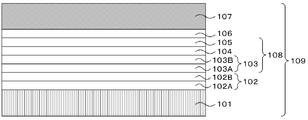
- the substrate was transferred to an HVPE furnace, and a window layer / support substrate 107 made of p-type GaP was grown by 120 ⁇ m to obtain an epitaxial substrate 109 (see FIG. 3).
- the active layer 104 has a multilayer structure made of AlGaInP.
- the first semiconductor layer has a two-layer structure including a low Al composition layer 103A and a high Al composition layer 103B.
- the high Al composition layer 103B has a multilayer structure made of (Al x Ga 1-x ) 0.5 In 0.5 P (0.70 ⁇ x ⁇ 1) with a thickness of 2.0 ⁇ m, and the low Al composition layer 103A has a thickness of The thickness was 0.6 ⁇ m (Al 0.4 Ga 0.6 ) 0.5 In 0.5 P.
- the second semiconductor layer 105 has a multilayer structure of (Al x Ga 1-x ) 0.5 In 0.5 P (0.3 ⁇ x ⁇ 1) having a thickness of 1.5 ⁇ m.
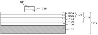
- the substrate 101, the GaAs buffer layer, and the second selective etching layer 102A were removed by etching to produce a light emitting element substrate 110 in which the first selective etching layer 102B remained (see FIG. 4).
- a first ohmic electrode 121 is formed on the first selective etching layer 102B of the light emitting element substrate 110 (see FIG. 5), and the first selective etching layer 102B is selected by SPM processing using the first ohmic electrode 121 as a mask. Removed.
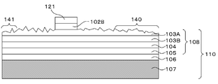
- a first roughening treatment step was performed on the surface of the low Al composition layer 103A located in the uppermost layer of the first semiconductor layer 103 (see FIG. 6).
- the first rough surface liquid a mixed liquid of acetic acid and hydrochloric acid was prepared, and the rough surface treatment was realized by etching for 1 minute at room temperature.
- the roughness Ra of the rough surface of the surface of the first semiconductor layer 103 at this time was measured. Further, the maximum value, minimum value, and average value of the etching depth at this time were also measured.
- the shallowest point of the unevenness formed by the first roughening process is the minimum value of the etching depth
- the deepest point is the maximum value
- the vicinity of the middle point between the shallowest point and the deepest point is the average value of the etching depth.
- R a of the example was 0.32 ⁇ m.
- the maximum value of the etching depth was 0.54 ⁇ m, the minimum value was 0.11 ⁇ m, and the average value was 0.41 ⁇ m.
- R a 0.33 ⁇ m, which is the same value as the example, but in order to realize this roughness, the average of the etching depth of the first roughening treatment is 0. .92 ⁇ m.
- the etching depth required in order to obtain a desired rough surface shape was able to be suppressed.
- a region other than the second ohmic electrode formation region 140 and the scribe region 141 is covered with a resist, and an element isolation step is performed by a wet etching method using a wet etching solution containing hydrochloric acid.
- the light emitting portion 108 was removed to form a removal portion 170 where the window layer / support substrate 107 was exposed, and other non-removal portions 180 (see FIG. 7).
- the 2nd ohmic electrode 122 was formed in the removal part 170 (refer FIG. 8).
- an insulating protective film 150 made of SiO 2 was laminated, and the surface of the first semiconductor layer 103 and the side surfaces of the light emitting unit 108 were covered with the insulating protective film 150.
- an opening was formed in the insulating protective film 150 in the first ohmic electrode 121 by photolithography and hydrofluoric acid etching.
- a scribe line was scribed along the exposed removed portion 170, the crack line was extended along the scribe line, and then the elements were separated by braking to form a light emitting element die.
- the light emitting element die was transferred to the holding tape so that the surface on which the first ohmic electrode was provided was on the tape surface side, and then the second roughening treatment step was performed.
- a rough surface solution used for roughening the window layer / supporting substrate in the second roughening treatment step a mixed solution of acetic acid, hydrofluoric acid, and iodine was prepared.
- the 2nd roughening process was performed by etching for 1 minute at normal temperature.
- R a 0.5 ⁇ m.
- a light emitting device was manufactured in the same process as in the example except that an n-type cladding layer having the same thickness as that of the example was formed without forming the low Al composition layer in the first roughened layer. Thereafter, wire bonding was performed in the same manner as in Example to produce an LED chip.
- the surface roughness after the first roughening treatment was measured, and the measurement results are shown in Table 1 as described above.
- the roughness Ra after the first roughening treatment was 0.33.
- the maximum value of the etching depth of the first roughening treatment was 1.17 ⁇ m, the minimum value was 0.71 ⁇ m, and the average value was 0.92 ⁇ m.
- the present invention is not limited to the above embodiment.
- the above-described embodiment is an exemplification, and the present invention has any configuration that has substantially the same configuration as the technical idea described in the claims of the present invention and that exhibits the same effects. Are included in the technical scope.
Landscapes
- Led Devices (AREA)
- Weting (AREA)
Abstract
本発明は、窓層兼支持基板と、該窓層兼支持基板上に設けられ、第二導電型の第二半導体層と、活性層と、第一導電型の第一半導体層とをこの順に含む発光部とを有する発光素子において、前記第一半導体層上に第一オーミック電極が設けられ、前記第一半導体層の表面及び前記発光部の側面の少なくとも一部は絶縁保護膜で被覆され、前記第一半導体層の表面及び前記窓層兼支持基板の表面が粗面化され、前記第一半導体層は、少なくとも二層以上の構造からなり、粗面化処理が施された側の層が、活性層側の層に比べ、Al組成が少ない材料からなるものであることを特徴とする発光素子である。これにより、クラッド層のキャリア閉じ込め効果を維持しつつ、所望の粗面形状を得るために必要なエッチング深さを抑制し、ワイヤーボンディング時にチップ割れが生じることを抑制した発光素子が提供される。
Description
本発明は、発光素子、及び発光素子の製造方法に関し、特に基板上にエピタキシャル成長によって第一半導体層、活性層、第二半導体層、窓層兼支持基板を形成し、基板を除去した後に電極を形成した発光素子基板へ粗面化処理を施す際の構造及び製造方法に関する。
近年、発光ダイオード(LED)の高効率化が進み、照明器具への適用が進んでいる。従来の照明器具はInGaN系の青色LEDと蛍光剤を組み合わせた器具がほとんどであった。しかし、蛍光剤を使用した際には原理的にストークスロスの発生が避けられず、蛍光剤が受光した全ての光を別の波長に変換はできない問題があった。特に青色より相対的に長波長の黄色や赤色といった領域でこの問題が顕著である。
この問題を解決するために、黄色や赤色LEDと青色LEDを組み合わせる技術が近年採用されている。その際、COB(chip on board)型のように一方の面に光を取り出すのではなく、ボードの上にLEDを並べてフィラメント型で発光させる電球タイプの照明器具が普及しつつある。このタイプの器具に適用するLED素子は、フィラメント全面にわたって光を取り出す必要があるため、素子の一方に光を取り出すタイプは適しておらず、チップの全方位に光を取り出す配光を有する素子が理想的である。
青色LEDであるInGaN系LEDはサファイア基板を用いるのが一般的であり、サファイア基板は発光波長に対して透明であるため、前述の照明器具に対しては理想的な形態になっている。しかし、黄色や赤色のLEDにおいては、発光波長に対して光吸収基板となるGaAsやGeを出発基板にしており、前記の用途には適さない。
この問題を解決するために、特許文献1に示すように発光部に透明基板を接合する方法や、特許文献2に示すように支持基板に用いられるような厚さまで窓層を成長し、光吸収基板である出発基板を除去してLEDにする技術が開示されている。
特許文献1で開示される方法では、必要な厚さ以上の透明基板を接合する必要があり、接合後に基板を所定の厚さまで削る必要があるため、コストアップの要因となる。また、通常、接合に用いられる基板は200μm以上の厚さがある。LED素子に要求される膜厚は、配光特性及び他の素子とのアセンブリ性を考慮すると、せいぜい100μm前後であるため、この程度の厚さまで薄膜化加工する必要がある。薄膜化加工にあたり、加工を行うことによる工数の増加、及び、ウェーハが割れるリスクも増大し、コストアップ及び歩留まり低下要因となる。
一方、特許文献2に開示される支持基板に用いることができる厚さまで結晶成長により成長した窓層を支持基板として利用する方法では、所望の厚さまで窓層を成長すればよく、薄膜化加工や基板接合・接着の工程が不要のため、低コストでの形成が可能であり、優れた方法である。
また、前述のような透明支持基板を有する発光素子においては、発光素子内部での多重反射を防止し、光吸収を抑制することで発光効率を上げる手法が取られるのが一般的である。特許文献3では、厚い窓層兼電流拡散層と厚い窓層兼支持基板が発光部を挟む構造において、窓層兼電流拡散層及び窓層兼支持基板に粗面をかけ、発光部には粗面をかけない方法が提案されている。ただ、この方法は窓層兼電流拡散層部を貫通する深いトレンチを形成する必要があり、コストがかかるだけでなく、上部と下部の電極の高低差が大きすぎるため、ワイヤーボンディングを行うことが難しい。フリップチップ型に適用するに際しても、厚い絶縁膜と非常に長い金属ビアを形成する必要があり、コストアップ要因となる。従って、上部電極部である窓層兼電流拡散層部が薄いことが望まれる。
窓層兼電流拡散層の厚さが薄く、上部電極部と下部電極部の高低差が少なく、かつ、光取り出し部もしくは光反射部に粗面を有する開示技術として、特許文献4及び5が挙げられる。特許文献4では、光取り出し面側と反対側のn型半導体層表面に粗面を形成しているが、フリップチップ型への技術開示であり、電極側から窓層側への効率的な光反射を目的としている。また、窓層兼支持基板と発光部両者へ粗面をかけることの難しさが開示されている。
特許文献5では、AlGaInP系クラッド層表面の粗面化処理を施す技術が開示されており、特許文献5によればクラッド層を(Al0.5Ga0.5)0.5In0.5Pとし、クラッド層上部に(AlxGa1-x)0.5In0.5P(0.5<x)からなるウインドウ層を積層する技術が開示されている。すなわち、粗面化処理を施す層がクラッド層より高いAl組成からなる層であることに関する技術について開示している。
しかしながら、窓層兼支持基板部と発光部を有する設計の発光素子において、発光部表面に細線を伴う電極を配置し、発光部にエッチングによって粗面化処理を行う場合においては、Al含有比率が高くなるほど、エッチング速度が速くなり、粗面をかけづらくなる傾向がある。このため、所望の粗面を得るためには、エッチング深さを増大させる必要がある。その結果、パッド電極形成面より大きく過度のエッチングがされるため、パッド電極部の機械強度が低下してしまう。これによって、ワイヤーボンディング時にチップ割れが生じるリスクが増大するという問題がある。
一方、活性層に注入したキャリアを閉じ込める効果を高めるためには、クラッド層のAl含有量を高める必要がある。しかしながら、上述したように、Al含有量を高めた場合、所望の粗面を得るためには、エッチング深さが大きくなるため、これに応じてクラッド層の厚さを、キャリア閉じ込め機能に対して必要最低限の厚さより大幅に厚くする必要もある。
従って、クラッド層のキャリア閉じ込め効果を維持し、ボンディングパッドの機械強度を維持しつつ、効果的に粗面をかけることができる技術はこれまでに開示されていない。
本発明は上記問題に鑑みてなされたものであって、窓層兼支持基板と発光部を有し、発光部の表面に粗面液(エッチング液)で粗面を形成する際に、クラッド層のキャリア閉じ込め効果を維持しつつ、所望の粗面形状を得るために必要なエッチング深さを抑制し、ワイヤーボンディング時にチップ割れが生じることを抑制した発光素子を提供することを目的とする。
上記目的を達成するために、本発明によれば、窓層兼支持基板と、該窓層兼支持基板上に設けられ、第二導電型の第二半導体層と、活性層と、第一導電型の第一半導体層とをこの順に含む発光部とを有する発光素子において、
前記第一半導体層上に第一オーミック電極が設けられ、前記第一半導体層の表面及び前記発光部の側面の少なくとも一部は絶縁保護膜で被覆され、前記第一半導体層の表面及び前記窓層兼支持基板の表面が粗面化され、
前記第一半導体層は、少なくとも二層以上の構造からなり、粗面化処理が施された側の層が、活性層側の層に比べ、Al組成が少ない材料からなるものであることを特徴とする発光素子を提供する。
前記第一半導体層上に第一オーミック電極が設けられ、前記第一半導体層の表面及び前記発光部の側面の少なくとも一部は絶縁保護膜で被覆され、前記第一半導体層の表面及び前記窓層兼支持基板の表面が粗面化され、
前記第一半導体層は、少なくとも二層以上の構造からなり、粗面化処理が施された側の層が、活性層側の層に比べ、Al組成が少ない材料からなるものであることを特徴とする発光素子を提供する。
このような発光素子であれば、クラッド層のキャリア閉じ込め効果を維持しつつ、所望の粗面形状を得るために必要なエッチング深さを抑制し、ワイヤーボンディング時にチップ割れが生じることを抑制した発光素子とすることができる。
このとき、前記発光部の一部が除去された除去部と、該除去部以外の非除去部と、該非除去部の前記第一半導体層上に設けられた前記第一オーミック電極と、
前記除去部の前記窓層兼支持基板上または前記第二半導体層上に設けられた第二オーミック電極とを有するものであることが好ましい。
このようなものであれば、本発明が特に有効に作用する。
前記除去部の前記窓層兼支持基板上または前記第二半導体層上に設けられた第二オーミック電極とを有するものであることが好ましい。
このようなものであれば、本発明が特に有効に作用する。
このとき、前記第一半導体層の粗面化処理が施される側の層は、
(AlxGa1-x)yIn1-yP(0≦x<0.6、0.4≦y≦0.6)あるいはAlzGa1-zAs(0≦z≦0.3)からなり、
前記第一半導体層の活性層側の層は、
(AlxGa1-x)yIn1-yP(0.6≦x≦1、0.4≦y≦0.6)あるいはAlzGa1-zAs(0.3<z≦1)からなるものであることが好ましい。
このようなものであれば、クラッド層のキャリア閉じ込め効果を維持しつつ、所望の粗面形状を得るために必要なエッチング深さを抑制し、ワイヤーボンディング時にチップ割れが生じることを抑制した発光素子とすることが確実にできる。
(AlxGa1-x)yIn1-yP(0≦x<0.6、0.4≦y≦0.6)あるいはAlzGa1-zAs(0≦z≦0.3)からなり、
前記第一半導体層の活性層側の層は、
(AlxGa1-x)yIn1-yP(0.6≦x≦1、0.4≦y≦0.6)あるいはAlzGa1-zAs(0.3<z≦1)からなるものであることが好ましい。
このようなものであれば、クラッド層のキャリア閉じ込め効果を維持しつつ、所望の粗面形状を得るために必要なエッチング深さを抑制し、ワイヤーボンディング時にチップ割れが生じることを抑制した発光素子とすることが確実にできる。
また、本発明によれば、基板上に、該基板と格子整合系の材料で第一半導体層、活性層、第二半導体層を順次エピタキシャル成長により成長させて発光部を形成する工程と、該発光部の上に前記基板に対して非格子整合系の材料で窓層兼支持基板をエピタキシャル成長により形成する工程と、前記基板を除去する工程と、前記第一半導体層上に第一オーミック電極を形成する工程と、前記第一半導体層の表面に粗面化処理を行う第一粗面化処理工程と、前記発光部の一部を除去して除去部と、それ以外の非除去部を形成する素子分離工程と、前記発光部が除去された窓層兼支持基板上に第二オーミック電極を形成する工程と、前記第一半導体層表面及び前記発光部の側面の少なくとも一部を絶縁保護膜で被覆する工程と、前記窓層兼支持基板の表面及び側面を粗面化する第二粗面化処理工程からなり、
前記発光部を形成する工程において、
前記第一半導体層を、少なくとも二層以上の構造からなり、粗面化処理が施される側の層が、活性層側の層に比べ、Al組成が少ない材料からなるもので形成することを特徴とする発光素子の製造方法を提供する。
前記発光部を形成する工程において、
前記第一半導体層を、少なくとも二層以上の構造からなり、粗面化処理が施される側の層が、活性層側の層に比べ、Al組成が少ない材料からなるもので形成することを特徴とする発光素子の製造方法を提供する。
このような製造方法であれば、クラッド層のキャリア閉じ込め効果を維持しつつ、所望の粗面形状を得るために必要なエッチング深さを抑制し、ワイヤーボンディング時にチップ割れが生じることを抑制した発光素子を製造することができる。
このとき、前記第一半導体層の粗面化処理が施される側の層を、
(AlxGa1-x)yIn1-yP(0≦x<0.6、0.4≦y≦0.6)あるいはAlzGa1-zAs(0≦z≦0.3)とし、
前記第一半導体層の活性層側の層を、
(AlxGa1-x)yIn1-yP(0.6≦x≦1、0.4≦y≦0.6)あるいはAlzGa1-zAs(0.3<z≦1)とすることが好ましい。
このようなものであれば、クラッド層のキャリア閉じ込め効果を維持しつつ、所望の粗面形状を得るために必要なエッチング深さを抑制し、ワイヤーボンディング時にチップ割れが生じることを抑制した発光素子を確実に製造することができる。
(AlxGa1-x)yIn1-yP(0≦x<0.6、0.4≦y≦0.6)あるいはAlzGa1-zAs(0≦z≦0.3)とし、
前記第一半導体層の活性層側の層を、
(AlxGa1-x)yIn1-yP(0.6≦x≦1、0.4≦y≦0.6)あるいはAlzGa1-zAs(0.3<z≦1)とすることが好ましい。
このようなものであれば、クラッド層のキャリア閉じ込め効果を維持しつつ、所望の粗面形状を得るために必要なエッチング深さを抑制し、ワイヤーボンディング時にチップ割れが生じることを抑制した発光素子を確実に製造することができる。
このとき、前記第一粗面化処理工程は、
有機酸と無機酸の混合液が用いられ、前記有機酸は、クエン酸・マロン酸・蟻酸・酢酸・酒石酸のいずれか一種類以上含有し、前記無機酸は塩酸・硫酸・硝酸・弗酸のいずれか一種類以上を含有する溶液を用いて行い、
前記第二粗面化処理工程は、
有機酸と無機酸を含む混合液が用いられ、前記有機酸は、クエン酸・マロン酸・蟻酸・酢酸・酒石酸のいずれか1種類以上を含み、かつ、前記無機酸は塩酸、硫酸、硝酸、弗酸のいずれか1種類以上を含み、かつ、沃素を含む溶液を用いて行うことが好ましい。
有機酸と無機酸の混合液が用いられ、前記有機酸は、クエン酸・マロン酸・蟻酸・酢酸・酒石酸のいずれか一種類以上含有し、前記無機酸は塩酸・硫酸・硝酸・弗酸のいずれか一種類以上を含有する溶液を用いて行い、
前記第二粗面化処理工程は、
有機酸と無機酸を含む混合液が用いられ、前記有機酸は、クエン酸・マロン酸・蟻酸・酢酸・酒石酸のいずれか1種類以上を含み、かつ、前記無機酸は塩酸、硫酸、硝酸、弗酸のいずれか1種類以上を含み、かつ、沃素を含む溶液を用いて行うことが好ましい。
このようにすれば、確実に求める凹凸の大きさの粗面を有する発光素子を製造することができる。
本発明によれば、クラッド層のキャリア閉じ込め効果を維持しつつ、所望の粗面形状を得るために必要なエッチング深さを抑制し、ワイヤーボンディング時にチップ割れが生じることを抑制した発光素子を実現できる。
また、本発明の発光素子の製造方法では、クラッド層のキャリア閉じ込め効果を維持しつつ、所望の粗面形状を得るために必要なエッチング深さを抑制し、ワイヤーボンディング時にチップ割れが生じることを抑制した発光素子を製造することができる。
また、本発明の発光素子の製造方法では、クラッド層のキャリア閉じ込め効果を維持しつつ、所望の粗面形状を得るために必要なエッチング深さを抑制し、ワイヤーボンディング時にチップ割れが生じることを抑制した発光素子を製造することができる。
以下、本発明について実施の形態を説明するが、本発明はこれに限定されるものではない。
前述のように、近年、粗面液で発光部に粗面を形成した場合、粗面を形成した層のAl組成がクラッド層部と同等かそれ以上のAl組成を有する場合、エッチングが速すぎることの影響により、粗面の凹凸差異が減少し、効果的に粗面化処理ができない問題があった。そこで、本発明者らは、粗面エッチング時の速いエッチング速度と、それに伴う凹凸不足を防止するために鋭意検討を重ねた。
その結果、発光部上面に粗面を形成する際に、第一半導体層を二種類以上のAl組成を有する層で構成し、第一半導体層の粗面化処理が施される側の層の材料が活性層側の層の材料よりAl組成が少ない材料であれば、クラッド層のキャリア閉じ込め効果を維持しつつ、過度のエッチングにより、パッド電極部の機械強度が低下し、ワイヤーボンディング時にチップ割れが生じることを抑制し、求める凹凸を有する粗面を得ることができるということに想到した。そして、これらを実施するための最良の形態について精査し、本発明を完成させた。
まず、本発明の発光素子について図1を参照して説明する。
図1に示すように、本発明の発光素子1は、窓層兼支持基板107と、窓層兼支持基板107上に設けられ、第二導電型の第二半導体層105と、活性層104と、第一導電型の第一半導体層103とをこの順に含む発光部108とを有している。
図1に示すように、本発明の発光素子1は、窓層兼支持基板107と、窓層兼支持基板107上に設けられ、第二導電型の第二半導体層105と、活性層104と、第一導電型の第一半導体層103とをこの順に含む発光部108とを有している。
第一半導体層103上には、第一オーミック電極121が設けられている。また、第一半導体層103表面及び発光部108の側面の少なくとも一部は絶縁保護膜150で被覆され、第一半導体層103の表面と、窓層兼支持基板107の表面及び側面が粗面化されたものである。
第一オーミック電極121は、図1に示すように、第一半導体層103上に、第一選択エッチング層102Bを介して設けたものであっても良い。
第一オーミック電極121は、図1に示すように、第一半導体層103上に、第一選択エッチング層102Bを介して設けたものであっても良い。
ここで、第一半導体層103は、図1に示すように、少なくとも二層以上の構造からなるものである。そして、粗面化処理が施された側の層(以下、低Al組成層103Aという)が、活性層側の層(以下、高Al組成層103Bという)に比べ、Al組成が少ない材料からなるものである。
具体的には、低Al組成層103Aは、(AlxGa1-x)yIn1-yP(0≦x<0.6、0.4≦y≦0.6)あるいはAlzGa1-zAs(0≦z≦0.3)からなり、高Al組成層103Bは、(AlxGa1-x)yIn1-yP(0.6≦x≦1、0.4≦y≦0.6)あるいはAlzGa1-zAs(0.3<z≦1)からなるものとすることができる。
発光素子1は、発光部108の少なくとも第一半導体層103と活性層104が除去された除去部170と、除去部170以外の非除去部180とが形成されたものであることが好ましい。なお、活性層104までを除去した場合、除去部170の表面は第二半導体層105となり緩衝層106まで除去した場合、除去部170の表面は窓層兼支持基板107となる。
そして、非除去部180の第一半導体層103上に設けられた第一オーミック電極121と、除去部170の窓層兼支持基板107上または第二半導体層105上に設けられた第二オーミック電極122とを有するものであることが好ましい。
このようなものであれば、本発明が特に有効に作用する。
そして、非除去部180の第一半導体層103上に設けられた第一オーミック電極121と、除去部170の窓層兼支持基板107上または第二半導体層105上に設けられた第二オーミック電極122とを有するものであることが好ましい。
このようなものであれば、本発明が特に有効に作用する。
このような本発明の発光素子であれば、クラッド層のキャリア閉じ込め効果を維持しつつ、所望の粗面形状を得るために必要なエッチング深さを抑制し、ワイヤーボンディング時にチップ割れが生じることを抑制した発光素子を実現することができる。
次に、本発明の発光素子の製造方法について図2-図8を参照して説明する。
まず、図3に示すように出発基板として、基板101を用意する(図2のSP1)。
まず、図3に示すように出発基板として、基板101を用意する(図2のSP1)。
基板101としては、GaAsまたはGeを好適に用いることができる。
このようにすれば、後述する活性層104の材料を格子整合系でエピタキシャル成長を行うことができるため、活性層104の品質を向上させやすく、輝度上昇や寿命特性の向上が得られる。
このようにすれば、後述する活性層104の材料を格子整合系でエピタキシャル成長を行うことができるため、活性層104の品質を向上させやすく、輝度上昇や寿命特性の向上が得られる。
次に、基板101の上に選択エッチング層102を形成してもよい(図2のSP2)。
選択エッチング層102は、基板101の上に、例えばMOVPE法(有機金属気相成長法)やMBE(分子線エピタキシー法)、CBE(化学線エピタキシー法)により形成することができる。
選択エッチング層102は、二層以上の層構造から成り、基板101に接する第二選択エッチング層102Aと、後述する第一半導体層103に接する第一選択エッチング層102Bを少なくとも有することが好ましい。第二選択エッチング層102Aと第一選択エッチング層102Bは異なる材料あるいは組成から構成しても良い。
選択エッチング層102は、基板101の上に、例えばMOVPE法(有機金属気相成長法)やMBE(分子線エピタキシー法)、CBE(化学線エピタキシー法)により形成することができる。
選択エッチング層102は、二層以上の層構造から成り、基板101に接する第二選択エッチング層102Aと、後述する第一半導体層103に接する第一選択エッチング層102Bを少なくとも有することが好ましい。第二選択エッチング層102Aと第一選択エッチング層102Bは異なる材料あるいは組成から構成しても良い。
次に、基板101と格子整合系の第一導電型の第一半導体層103、活性層104、第二導電型の第二半導体層105を順次エピタキシャル成長により成長させて発光部108を形成する(図2のSP3)。
次に、発光部108の上に基板101に対して非格子整合系の材料で窓層兼支持基板107をエピタキシャル成長により形成して、エピタキシャル基板109を作製する(図2のSP4)。
上記SP3、4において、具体的には、図3に示すように、第一導電型の第一半導体層103、活性層104、第二導電型の第二半導体層105からなる発光部108上に、緩衝層106、窓層兼支持基板107をこの順にエピタキシャル成長したエピタキシャル基板109を作製することができる。
なお、窓層兼支持基板107は、HVPE法(ハイドライド気相成長法)により形成してもよい。
なお、窓層兼支持基板107は、HVPE法(ハイドライド気相成長法)により形成してもよい。
活性層104は発光波長に応じて(AlxGa1-x)yIn1-yP(0≦x≦1、0.4≦y≦0.6)またはAlzGa1―zAs(0≦z≦0.45)で形成することができる。例えば、可視光照明に適用する場合、AlGaInPを選択するのが好適であり、赤外照明に適用する場合、AlGaAsを選択するのが好適である。ただし、活性層104の設計に関しては、超格子等の利用により波長は材料組成に起因する波長以外に調整可能であるため、上記の材料に限られない。
第一半導体層103、第二半導体層105はAlGaInPもしくはAlGaAsが選択され、その選択は活性層104と必ずしも同一の材料系でなくともよい。
本実施形態においては、最も単純な構造である第一半導体層103、活性層104、第二半導体層105が同一材料であるAlGaInPの場合を例示するが、第一半導体層103あるいは第二半導体層105は特性向上のため、各層内には複数層が含まれるのが一般的であり、第一半導体層103あるいは第二半導体層105が単一層であることに限定されないことは言うまでもない。
このとき、第一半導体層103は二層以上の構造からなるものとする。第一半導体層103の粗面化処理が施される側の低Al組成層103Aが、活性層側の高Al組成層103Bに比べ、Al組成が少ない材料からなるもので形成する。
ここで、高Al組成層103Bはクラッド層の機能を有する機能層であり、単一組成あるいは単一条件層に限定されない。
ここで、高Al組成層103Bはクラッド層の機能を有する機能層であり、単一組成あるいは単一条件層に限定されない。
具体的には、低Al組成層103Aを、(AlxGa1-x)yIn1-yP(0≦x<0.6、0.4≦y≦0.6)あるいはAlzGa1-zAs(0≦z≦0.3)とし、高Al組成層103Bを、(AlxGa1-x)yIn1-yP(0.6≦x≦1、0.4≦y≦0.6)あるいはAlzGa1-zAs(0.3<z≦1)とすることができる。
窓層兼支持基板107としては、GaP、GaAsP、AlGaAs、サファイア(Al2O3)、石英(SiO2)、SiC等を好適に用いることができる。窓層兼支持基板107をGaAsPまたはGaPで形成した場合、緩衝層106はGaInPで形成するのが最も好適であるが、緩衝層106は、緩衝機能のある材料であればいかなる材料の選択も可能で、これに限定されないことは言うまでもない。
また、窓層兼支持基板107として、GaAsPを選択すると、耐候性が良好である。
しかし、GaAsPと、AlGaInP系材料またはAlGaAs系材料との間には大きな格子不整合が存在するため、GaAsPには高密度のひずみや貫通転位が入る。その結果、エピタキシャル基板109は大きな反りを有する。
また、窓層兼支持基板107として、GaAsPを選択すると、耐候性が良好である。
しかし、GaAsPと、AlGaInP系材料またはAlGaAs系材料との間には大きな格子不整合が存在するため、GaAsPには高密度のひずみや貫通転位が入る。その結果、エピタキシャル基板109は大きな反りを有する。
ここで、自然超格子の形成による波長シフトを防止するため、発光部108は、成長面に対して結晶学的に12度以上傾斜して成長が行われることが好ましい。この傾斜方向は、どの方向に選択することも可能だが、スクライブ・ブレーキング工程で素子を分離する工程を採用する場合、スクライブ線の一方には結晶軸が傾斜せず直交する方向を選択し、スクライブ線の他方には結晶軸が傾斜する方向を選択すれば、素子側面が素子表面及び裏面に対して傾斜する面を少なくできる。従って、通常はスクライブ線の一方は傾斜しない方向が選択されるが、20度程度の素子側面の傾斜は、アセンブリ上は大きな問題にならない。従って、上記直交方向は、厳密に一致する必要はなく、直交方向より±20度程度の角度範囲は直交方向に概念的に含まれる。
次に、エピタキシャル基板109から基板101及び第二選択エッチング層102Aを除去して、図4に示すように発光素子基板110の第一半導体層103の表面に第一選択エッチング層102Bのみを残留させる(図2のSP5)。
具体的には、エピタキシャル基板109から第二選択エッチング層102Aを用いてウェットエッチング法により基板101を除去することで、第一半導体層103の表面に第一選択エッチング層102Bのみを残留させることができる。
具体的には、エピタキシャル基板109から第二選択エッチング層102Aを用いてウェットエッチング法により基板101を除去することで、第一半導体層103の表面に第一選択エッチング層102Bのみを残留させることができる。
次に、図5に示すように、第一半導体層103上の第一選択エッチング層102Bの表面に、発光素子へ電位を供給するための第一オーミック電極121を形成する(図2のSP6)。
次に、図5に示すように、第一オーミック電極121の下部以外の領域の第一選択エッチング層102Bを除去する(図2のSP7)。
具体的には、第一オーミック電極121をエッチングマスクとし、第一オーミック電極121の下部以外の領域の第一選択エッチング層102Bを、エッチングにより除去することができる。
具体的には、第一オーミック電極121をエッチングマスクとし、第一オーミック電極121の下部以外の領域の第一選択エッチング層102Bを、エッチングにより除去することができる。
次に、図6に示すように第一半導体層103の表面に粗面化処理を行う第一粗面化処理工程を行う(図2のSP8)。
第一粗面化処理工程は、有機酸と無機酸の混合液が用いられ、前記有機酸としてカルボン酸、特には、クエン酸・マロン酸・蟻酸・酢酸・酒石酸のいずれか一種類以上含有し、前記無機酸は塩酸・硫酸・硝酸・弗酸のいずれか一種類以上を含有する溶液を用いて行うことができる。
このようにすれば、確実に表面を粗面化することができる。
このようにすれば、確実に表面を粗面化することができる。
このとき、第一粗面液は主として低Al組成層103Aに対して第一粗面化処理を施すことが好ましい。低Al組成層103Aと高Al組成層103Bが同系統の材料、例えば、両者共にAlGaInP系の材料で形成した場合、高Al組成層103Bの方が低Al組成層103Aよりエッチングが速くなるため、高Al組成層103Bへのエッチングが好ましくない場合は低Al組成層103Aの厚さを、エッチング予定幅より厚く形成することが好ましい。
一方、低Al組成層103Aで生じた凹凸をエッチング用パターンとして高Al組成層103Bの一部をエッチングし、凹凸を大きくしたい場合は、エッチング予定幅より薄く低Al組成層103Aを形成することが好ましい。
一方、低Al組成層103Aで生じた凹凸をエッチング用パターンとして高Al組成層103Bの一部をエッチングし、凹凸を大きくしたい場合は、エッチング予定幅より薄く低Al組成層103Aを形成することが好ましい。
なお、第一粗面化処理工程において、粗面の凹凸の大きさは、低Al組成層103AのAl含有率により決定することができる。例えば、粗さRa(算術平均粗さ)を0.3μm程度にするためには、前記組成の低Al組成層103Aに対して、例えば、0.3~0.6μmの幅のエッチング深さでエッチングすると良い。
一方、エッチング深さを0.3~0.6μmの幅より小さくすればRaを小さくすることができる。また、エッチング深さを0.3~0.6μmの幅より大きくすれば、粗面が平坦化するため、Raを小さくすることができる。
Raを大きくする場合、低Al組成層103Aをエッチング予定幅よりわずかに薄く形成する。低Al組成層のエッチング速度は遅く、高Al組成層のエッチング速度は速いため、低Al組成層がエッチングにより失われた部分からエッチング速度が速くなり、前記部分が深くエッチングされるため、Raを大きくすることができる。
一方、エッチング深さを0.3~0.6μmの幅より小さくすればRaを小さくすることができる。また、エッチング深さを0.3~0.6μmの幅より大きくすれば、粗面が平坦化するため、Raを小さくすることができる。
Raを大きくする場合、低Al組成層103Aをエッチング予定幅よりわずかに薄く形成する。低Al組成層のエッチング速度は遅く、高Al組成層のエッチング速度は速いため、低Al組成層がエッチングにより失われた部分からエッチング速度が速くなり、前記部分が深くエッチングされるため、Raを大きくすることができる。
なお、第一選択エッチング層102Bを第一粗面液に対して選択エッチング性がある材料で構成することで、第一粗面液は第一オーミック電極の形状に沿ってファセット面を形成する。このようにして、第一選択エッチング層102Bを第一オーミック電極121の下部に設けることにより、第一オーミック電極121の下部へのオーバーエッチングの発生を防止することができるので、発光部表面の電極の剥離を抑制することができる。
次に、図7に示すように、発光部108の一部を除去して除去部170と、それ以外の非除去部180を形成する素子分離工程を行う(図2のSP9)。
素子分離工程は、例えば、フォトリソグラフィー法により、レジストで第一半導体層103上の所定の領域(図6における第二オーミック電極形成領域140、スクライブ領域141)を開口させたパターンを形成し、このレジストをエッチングマスクとして用いてエッチングすることによって行うことができる。
上記エッチングは、塩酸を含有するウェットエッチング液によるウェットエッチング法により、第二半導体層105、緩衝層106もしくは窓層兼支持基板107を露出させた除去部170と、除去部170以外の非除去部180を形成することができる。
上記エッチングは、塩酸を含有するウェットエッチング液によるウェットエッチング法により、第二半導体層105、緩衝層106もしくは窓層兼支持基板107を露出させた除去部170と、除去部170以外の非除去部180を形成することができる。
また、素子分離工程は、上記で例示したウェットエッチング法の他、ハロゲンガス、好ましくは塩化水素を含有するガスを用いるRIE法もしくはICP法等の、ドライエッチング法にて行うこともできる。
次に、図8に示すように、発光部108が除去された窓層兼支持基板107上または第二半導体層105上の除去部170上に第二オーミック電極122を形成する(図2のSP10)。
次に、図8に示すように、第一半導体層103表面及び発光部108の側面の少なくとも一部を絶縁保護膜150で被覆する(図2のSP11)。
絶縁保護膜150は透明で絶縁性を有する材料であれば、どのような材料でも可能である。絶縁保護膜150としては、例えばSiO2もしくはSiNxを用いることが好適である。このようなものであれば、フォトリソグラフィー法と弗酸を含有したエッチング液によって、第一オーミック電極121の上部を開口する加工を容易に行うことができる。
絶縁保護膜150は透明で絶縁性を有する材料であれば、どのような材料でも可能である。絶縁保護膜150としては、例えばSiO2もしくはSiNxを用いることが好適である。このようなものであれば、フォトリソグラフィー法と弗酸を含有したエッチング液によって、第一オーミック電極121の上部を開口する加工を容易に行うことができる。
次に、図1に示すように、窓層兼支持基板107の表面及び側面を粗面化する第二粗面化処理工程を行う(図2のSP12)。
第二粗面化処理を行う前に、まず、除去部170に沿ってスクライブ線をけがき、ブレーキングを行うことで発光素子を分離して、発光素子ダイスを形成することが好ましい。発光素子ダイス形成後、窓層兼支持基板107が上面になるように発光素子ダイスを保持テープに転写してから、下記の第二粗面化処理を行うことが好ましい。
第二粗面化処理工程は、有機酸と無機酸を含む混合液が用いられ、前記有機酸は、クエン酸・マロン酸・蟻酸・酢酸・酒石酸のいずれか1種類以上を含み、かつ、前記無機酸は塩酸、硫酸、硝酸、弗酸のいずれか1種類以上を含み、かつ、沃素を含む溶液を用いて行うことができる。
このようにすれば、確実に表面を粗面化することができる。
このようにすれば、確実に表面を粗面化することができる。
上述した第一粗面化処理工程で用いた第一半導体層103に施す第一粗面液と、第二粗面化処理工程で窓層兼支持基板107に施す第二粗面液とは液組成が異なる。そのため、エッチング特性が異なるため、必然的に第一半導体層103と窓層兼支持基板107が有する粗面の形状及びRaは異なったものとなる。
上述したような方法により、クラッド層のキャリア閉じ込め効果を維持しつつ、過度のエッチングによる、パッド電極部の機械強度が低下し、ワイヤーボンディング時にチップ割れが生じることを抑制し、求める凹凸の大きさの粗面を得る発光素子を製造することができる。
以下、本発明の実施例及び比較例を示して本発明をより具体的に説明するが、本発明はこれらに限定されるものではない。
(実施例)
結晶軸が[001]方向より[110]方向に15°傾斜した厚さ280μmのn型GaAsからなる基板101上にn型GaAsバッファ層(不図示)を0.5μm、n型AlInP層からなる第二選択エッチング層102Aを1μm、n型GaAs層から成る第一選択エッチング層102Bを1μm成長させた後、MOVPE法でAlGaInPから成るn型クラッド層(第一半導体層103)、活性層104、p型クラッド層(第二半導体層105)で構成される発光部108を5.5μm形成し、更にp型GaInPからなる緩衝層106を0.3μm形成し、GaP窓層兼支持基板107の一部としてp型GaPからなる層を1μm形成した。次に、HVPE炉に移してp型GaPからなる窓層兼支持基板107を120μm成長させ、エピタキシャル基板109を得た(図3参照)。
結晶軸が[001]方向より[110]方向に15°傾斜した厚さ280μmのn型GaAsからなる基板101上にn型GaAsバッファ層(不図示)を0.5μm、n型AlInP層からなる第二選択エッチング層102Aを1μm、n型GaAs層から成る第一選択エッチング層102Bを1μm成長させた後、MOVPE法でAlGaInPから成るn型クラッド層(第一半導体層103)、活性層104、p型クラッド層(第二半導体層105)で構成される発光部108を5.5μm形成し、更にp型GaInPからなる緩衝層106を0.3μm形成し、GaP窓層兼支持基板107の一部としてp型GaPからなる層を1μm形成した。次に、HVPE炉に移してp型GaPからなる窓層兼支持基板107を120μm成長させ、エピタキシャル基板109を得た(図3参照)。
活性層104はAlGaInPから成る多層構造とした。
第一半導体層は、低Al組成層103Aと、高Al組成層103Bからなる二層構造とした。
高Al組成層103Bは厚さ2.0μmの(AlxGa1-x)0.5In0.5P(0.70≦x≦1)から成る多層構造とし、低Al組成層103Aは厚さ0.6μmの(Al0.4Ga0.6)0.5In0.5Pとした。
高Al組成層103Bは厚さ2.0μmの(AlxGa1-x)0.5In0.5P(0.70≦x≦1)から成る多層構造とし、低Al組成層103Aは厚さ0.6μmの(Al0.4Ga0.6)0.5In0.5Pとした。
第二半導体層105は厚さ1.5μmの(AlxGa1-x)0.5In0.5P(0.3≦x≦1)の多層構造とした。
次に、基板101、GaAsバッファ層および第二選択エッチング層102Aをエッチング除去して、第一選択エッチング層102Bを残留させた発光素子基板110を作製した(図4参照)。
次に、発光素子基板110の第一選択エッチング層102B上へ第一オーミック電極121を形成し(図5参照)、第一オーミック電極121をマスクとしてSPM処理にて第一選択エッチング層102Bを選択的に除去した。
次に、第一半導体層103の最も上の層に位置する低Al組成層103A表面に第一粗面化処理工程を施した(図6参照)。第一粗面液は酢酸と塩酸の混合液を作製し、常温で1分エッチングすることで粗面化処理を実現した。このときの第一半導体層103表面の粗面の粗さRaを測定した。
また、このときのエッチング深さの最大値、最小値及び、平均値についても測定した。なお、第一粗面化処理により形成された凹凸の最浅点をエッチング深さの最小値、最深点を最大値とし、最浅点と最深点の中間点付近をエッチング深さの平均値と定義した。
上記のようにして測定した結果を表1に示した。なお、表1には、後述する比較例の結果も併せて記した。
また、このときのエッチング深さの最大値、最小値及び、平均値についても測定した。なお、第一粗面化処理により形成された凹凸の最浅点をエッチング深さの最小値、最深点を最大値とし、最浅点と最深点の中間点付近をエッチング深さの平均値と定義した。
上記のようにして測定した結果を表1に示した。なお、表1には、後述する比較例の結果も併せて記した。

表1に示したように、実施例のRa=0.32μmであった。また、エッチング深さの最大値は、0.54μm、最小値は、0.11μm、平均値は0.41μmであった。一方、後述する比較例では、Ra=0.33μmと実施例と同程度の値であったが、この粗さを実現するために、第一粗面化処理のエッチング深さの平均は0.92μmであった。
このように、後述する比較例に比べて、実施例では、所望の粗面形状を得るために必要なエッチング深さを抑制することができた。
このように、後述する比較例に比べて、実施例では、所望の粗面形状を得るために必要なエッチング深さを抑制することができた。
次に、フォトリソグラフィー法により、第二オーミック電極形成領域140及びスクライブ領域141(図6参照)以外をレジストで被覆し、塩酸を含有するウェットエッチング液によるウェットエッチング法で素子分離工程を実施し、発光部108を除去して窓層兼支持基板107が露出した除去部170と、それ以外の非除去部180を形成した(図7参照)。
次に、除去部170に第二オーミック電極122を形成した(図8参照)。次に、SiO2からなる絶縁保護膜150を積層し、第一半導体層103表面及び発光部108の側面を絶縁保護膜150で被覆した。そして、第一オーミック電極121の部分をフォトリソグラフィー法と弗酸エッチングにより、絶縁保護膜150に開口部を形成した。
次に、露出させた除去部170に沿ってスクライブ線をけがき、スクライブ線に沿ってクラック線を伸ばし、その後、ブレーキングを行うことで素子を分離し、発光素子ダイスを形成した。
発光素子ダイス形成後、第一オーミック電極が設けられている面がテープ面側になるように保持テープに発光素子ダイスを転写し、その後、第二粗面化処理工程を実施した。第二粗面化処理工程で窓層兼支持基板の粗面化を行う際に用いる粗面液は、酢酸と弗酸、沃素の混合液を作製した。そして、常温で1分エッチングすることで第二粗面化処理を行った。このときの窓層兼支持基板107の表面および側面の粗面の粗さを測定したところ、Ra=0.5μmであった。
このように、クラッド層のキャリア閉じ込め効果を維持しつつ、所望の粗面形状を得るために必要なエッチング深さが抑制された発光素子を製造することができた。
このように、クラッド層のキャリア閉じ込め効果を維持しつつ、所望の粗面形状を得るために必要なエッチング深さが抑制された発光素子を製造することができた。
そして、ワイヤーボンディングを行い、LEDチップを製造した。
その結果、ワイヤーボンディング時にチップ割れを起こさずに、LEDチップを製造することができた。
その結果、ワイヤーボンディング時にチップ割れを起こさずに、LEDチップを製造することができた。
(比較例)
第一粗面化処理層に低Al組成層を形成せずに実施例と同じ厚さのn型クラッド層を形成したことを除き実施例と同様の工程で発光素子を製造した。
その後、実施例と同様にして、ワイヤーボンディングを行い、LEDチップを作製した。
第一粗面化処理層に低Al組成層を形成せずに実施例と同じ厚さのn型クラッド層を形成したことを除き実施例と同様の工程で発光素子を製造した。
その後、実施例と同様にして、ワイヤーボンディングを行い、LEDチップを作製した。
実施例と同様に、第一粗面化処理後の表面粗さを測定し、その測定結果を上記したように表1に示した。
表1に示したように、第一粗面化処理後の粗さRa=0.33であった。この粗さを実現するため第一粗面化処理のエッチング深さの最大値は、1.17μm、最小値は、0.71μm、平均値は0.92μmであった。
表1に示したように、第一粗面化処理後の粗さRa=0.33であった。この粗さを実現するため第一粗面化処理のエッチング深さの最大値は、1.17μm、最小値は、0.71μm、平均値は0.92μmであった。
また、実施例と同様に、第二粗面化処理後の粗さを測定したところ、Ra=0.5μmであった。
また、比較例では、ワイヤーボンディング時の衝撃吸収力が低下し、チップ割れを起こした。
また、比較例では、ワイヤーボンディング時の衝撃吸収力が低下し、チップ割れを起こした。
なお、本発明は、上記実施形態に限定されるものではない。上記実施形態は例示であり、本発明の特許請求の範囲に記載された技術的思想と実質的に同一な構成を有し、同様な作用効果を奏するものは、いかなるものであっても本発明の技術的範囲に包含される。
Claims (6)
- 窓層兼支持基板と、該窓層兼支持基板上に設けられ、第二導電型の第二半導体層と、活性層と、第一導電型の第一半導体層とをこの順に含む発光部とを有する発光素子において、
前記第一半導体層上に第一オーミック電極が設けられ、前記第一半導体層の表面及び前記発光部の側面の少なくとも一部は絶縁保護膜で被覆され、前記第一半導体層の表面及び前記窓層兼支持基板の表面が粗面化され、
前記第一半導体層は、少なくとも二層以上の構造からなり、粗面化処理が施された側の層が、活性層側の層に比べ、Al組成が少ない材料からなるものであることを特徴とする発光素子。 - 前記発光部の一部が除去された除去部と、該除去部以外の非除去部と、該非除去部の前記第一半導体層上に設けられた前記第一オーミック電極と、
前記除去部の前記窓層兼支持基板上または前記第二半導体層上に設けられた第二オーミック電極とを有するものであることを特徴とする請求項1に記載の発光素子。 - 前記第一半導体層の粗面化処理が施される側の層は、
(AlxGa1-x)yIn1-yP(0≦x<0.6、0.4≦y≦0.6)あるいはAlzGa1-zAs(0≦z≦0.3)からなり、
前記第一半導体層の活性層側の層は、
(AlxGa1-x)yIn1-yP(0.6≦x≦1、0.4≦y≦0.6)あるいはAlzGa1-zAs(0.3<z≦1)からなるものであることを特徴とする請求項1又は請求項2に記載の発光素子。 - 基板上に、該基板と格子整合系の材料で第一半導体層、活性層、第二半導体層を順次エピタキシャル成長により成長させて発光部を形成する工程と、該発光部の上に前記基板に対して非格子整合系の材料で窓層兼支持基板をエピタキシャル成長により形成する工程と、前記基板を除去する工程と、前記第一半導体層上に第一オーミック電極を形成する工程と、前記第一半導体層の表面に粗面化処理を行う第一粗面化処理工程と、前記発光部の一部を除去して除去部と、それ以外の非除去部を形成する素子分離工程と、前記発光部が除去された窓層兼支持基板上に第二オーミック電極を形成する工程と、前記第一半導体層表面及び前記発光部の側面の少なくとも一部を絶縁保護膜で被覆する工程と、前記窓層兼支持基板の表面及び側面を粗面化する第二粗面化処理工程からなり、
前記発光部を形成する工程において、
前記第一半導体層を、少なくとも二層以上の構造からなり、粗面化処理が施される側の層が、活性層側の層に比べ、Al組成が少ない材料からなるもので形成することを特徴とする発光素子の製造方法。 - 前記第一半導体層の粗面化処理が施される側の層を、
(AlxGa1-x)yIn1-yP(0≦x<0.6、0.4≦y≦0.6)あるいはAlzGa1-zAs(0≦z≦0.3)とし、
前記第一半導体層の活性層側の層を、
(AlxGa1-x)yIn1-yP(0.6≦x≦1、0.4≦y≦0.6)あるいはAlzGa1-zAs(0.3<z≦1)とすることを特徴とする請求項4に記載の発光素子の製造方法。 - 前記第一粗面化処理工程は、
有機酸と無機酸の混合液が用いられ、前記有機酸は、クエン酸・マロン酸・蟻酸・酢酸・酒石酸のいずれか一種類以上含有し、前記無機酸は塩酸・硫酸・硝酸・弗酸のいずれか一種類以上を含有する溶液を用いて行い、
前記第二粗面化処理工程は、
有機酸と無機酸を含む混合液が用いられ、前記有機酸は、クエン酸・マロン酸・蟻酸・酢酸・酒石酸のいずれか1種類以上を含み、かつ、前記無機酸は塩酸、硫酸、硝酸、弗酸のいずれか1種類以上を含み、かつ、沃素を含む溶液を用いて行うことを特徴とする請求項4又は請求項5に記載の発光素子の製造方法。
Priority Applications (2)
| Application Number | Priority Date | Filing Date | Title |
|---|---|---|---|
| CN201580069819.6A CN107112389B (zh) | 2015-01-09 | 2015-12-09 | 发光组件以及发光组件的制造方法 |
| US15/538,032 US10388831B2 (en) | 2015-01-09 | 2015-12-09 | Light-emitting device and method for manufacturing light-emitting device |
Applications Claiming Priority (2)
| Application Number | Priority Date | Filing Date | Title |
|---|---|---|---|
| JP2015-003128 | 2015-01-09 | ||
| JP2015003128A JP6197799B2 (ja) | 2015-01-09 | 2015-01-09 | 発光素子及び発光素子の製造方法 |
Publications (1)
| Publication Number | Publication Date |
|---|---|
| WO2016110896A1 true WO2016110896A1 (ja) | 2016-07-14 |
Family
ID=56355628
Family Applications (1)
| Application Number | Title | Priority Date | Filing Date |
|---|---|---|---|
| PCT/JP2015/006121 Ceased WO2016110896A1 (ja) | 2015-01-09 | 2015-12-09 | 発光素子及び発光素子の製造方法 |
Country Status (5)
| Country | Link |
|---|---|
| US (1) | US10388831B2 (ja) |
| JP (1) | JP6197799B2 (ja) |
| CN (1) | CN107112389B (ja) |
| TW (1) | TWI663748B (ja) |
| WO (1) | WO2016110896A1 (ja) |
Cited By (2)
| Publication number | Priority date | Publication date | Assignee | Title |
|---|---|---|---|---|
| JP2022003678A (ja) * | 2020-06-23 | 2022-01-11 | 隆達電子股▲ふん▼有限公司 | 発光ダイオード |
| WO2025022808A1 (ja) * | 2023-07-21 | 2025-01-30 | ウシオ電機株式会社 | 赤外led素子 |
Families Citing this family (9)
| Publication number | Priority date | Publication date | Assignee | Title |
|---|---|---|---|---|
| JP6623973B2 (ja) * | 2016-08-19 | 2019-12-25 | 信越半導体株式会社 | 発光素子及び発光素子の製造方法 |
| JP2018170333A (ja) * | 2017-03-29 | 2018-11-01 | 株式会社東芝 | 半導体装置及びその製造方法 |
| KR102343099B1 (ko) * | 2017-06-07 | 2021-12-24 | 쑤저우 레킨 세미컨덕터 컴퍼니 리미티드 | 반도체 소자 |
| JP6648329B2 (ja) * | 2018-04-19 | 2020-02-14 | Dowaエレクトロニクス株式会社 | 半導体発光素子およびその製造方法 |
| DE102019114169A1 (de) * | 2019-05-27 | 2020-12-03 | OSRAM Opto Semiconductors Gesellschaft mit beschränkter Haftung | Optoelektronisches halbleiterbauelement mit verbindungsbereichen und verfahren zur herstellung des optoelektronischen halbleiterbauelements |
| US12068575B2 (en) | 2020-04-29 | 2024-08-20 | Phosertek Corporation | Laser device and method of manufacturing the same |
| TWM611530U (zh) * | 2020-04-29 | 2021-05-11 | 富昱晶雷射科技股份有限公司 | 覆晶型之電激發光子晶體面射型雷射元件 |
| US11705554B2 (en) | 2020-10-09 | 2023-07-18 | Sion Power Corporation | Electrochemical cells and/or components thereof comprising nitrogen-containing species, and methods of forming them |
| CN113066913A (zh) * | 2021-06-03 | 2021-07-02 | 南昌凯迅光电有限公司 | 一种N面出光AlGaInPLED薄膜芯片及制备方法 |
Citations (6)
| Publication number | Priority date | Publication date | Assignee | Title |
|---|---|---|---|---|
| JP2006270001A (ja) * | 2005-03-25 | 2006-10-05 | Tokyo Univ Of Science | 光取り出し効率及び放熱効果が改善された半導体発光素子およびその製造方法 |
| JP2008103627A (ja) * | 2006-10-20 | 2008-05-01 | Hitachi Cable Ltd | 半導体発光素子 |
| JP2009252860A (ja) * | 2008-04-03 | 2009-10-29 | Hitachi Cable Ltd | 半導体発光素子 |
| JP2011142231A (ja) * | 2010-01-07 | 2011-07-21 | Hitachi Cable Ltd | 半導体発光素子及びledランプ、並びに半導体発光素子の製造方法 |
| JP2012142508A (ja) * | 2011-01-06 | 2012-07-26 | Hitachi Cable Ltd | 半導体素子用ウェハ |
| JP2014195069A (ja) * | 2013-02-28 | 2014-10-09 | Asahi Kasei E-Materials Corp | 半導体発光素子及びその製造方法並びに光学基材 |
Family Cites Families (12)
| Publication number | Priority date | Publication date | Assignee | Title |
|---|---|---|---|---|
| JP4569858B2 (ja) | 2003-11-19 | 2010-10-27 | 信越半導体株式会社 | 発光素子の製造方法 |
| JP4715370B2 (ja) * | 2005-07-29 | 2011-07-06 | 信越半導体株式会社 | 発光素子及びその製造方法 |
| US7651964B2 (en) * | 2005-08-17 | 2010-01-26 | Milliken & Company | Fiber-containing composite and method for making the same |
| JP2007059518A (ja) | 2005-08-23 | 2007-03-08 | Showa Denko Kk | 半導体発光素子 |
| US7692203B2 (en) | 2006-10-20 | 2010-04-06 | Hitachi Cable, Ltd. | Semiconductor light emitting device |
| TWI419355B (zh) * | 2007-09-21 | 2013-12-11 | Nat Univ Chung Hsing | 高光取出率的發光二極體晶片及其製造方法 |
| KR101501307B1 (ko) * | 2007-09-21 | 2015-03-10 | 가부시끼가이샤 도시바 | 발광 장치 제작 방법 |
| JP2010251531A (ja) | 2009-04-16 | 2010-11-04 | Rohm Co Ltd | 半導体発光素子 |
| JP5427585B2 (ja) | 2009-12-18 | 2014-02-26 | 昭和電工株式会社 | フリップチップ型発光ダイオード及びその製造方法 |
| CN103117349A (zh) * | 2011-11-17 | 2013-05-22 | 大连美明外延片科技有限公司 | 一种高亮度AlGaInP发光二极管及其制造方法 |
| TWI637534B (zh) * | 2013-11-29 | 2018-10-01 | 晶元光電股份有限公司 | 發光裝置 |
| CN103715324B (zh) * | 2014-01-02 | 2017-02-22 | 厦门乾照光电股份有限公司 | 一种发光二极管及其制造方法 |
-
2015
- 2015-01-09 JP JP2015003128A patent/JP6197799B2/ja active Active
- 2015-12-09 WO PCT/JP2015/006121 patent/WO2016110896A1/ja not_active Ceased
- 2015-12-09 CN CN201580069819.6A patent/CN107112389B/zh active Active
- 2015-12-09 US US15/538,032 patent/US10388831B2/en active Active
- 2015-12-14 TW TW104141980A patent/TWI663748B/zh active
Patent Citations (6)
| Publication number | Priority date | Publication date | Assignee | Title |
|---|---|---|---|---|
| JP2006270001A (ja) * | 2005-03-25 | 2006-10-05 | Tokyo Univ Of Science | 光取り出し効率及び放熱効果が改善された半導体発光素子およびその製造方法 |
| JP2008103627A (ja) * | 2006-10-20 | 2008-05-01 | Hitachi Cable Ltd | 半導体発光素子 |
| JP2009252860A (ja) * | 2008-04-03 | 2009-10-29 | Hitachi Cable Ltd | 半導体発光素子 |
| JP2011142231A (ja) * | 2010-01-07 | 2011-07-21 | Hitachi Cable Ltd | 半導体発光素子及びledランプ、並びに半導体発光素子の製造方法 |
| JP2012142508A (ja) * | 2011-01-06 | 2012-07-26 | Hitachi Cable Ltd | 半導体素子用ウェハ |
| JP2014195069A (ja) * | 2013-02-28 | 2014-10-09 | Asahi Kasei E-Materials Corp | 半導体発光素子及びその製造方法並びに光学基材 |
Cited By (4)
| Publication number | Priority date | Publication date | Assignee | Title |
|---|---|---|---|---|
| JP2022003678A (ja) * | 2020-06-23 | 2022-01-11 | 隆達電子股▲ふん▼有限公司 | 発光ダイオード |
| JP7208961B2 (ja) | 2020-06-23 | 2023-01-19 | 隆達電子股▲ふん▼有限公司 | 発光ダイオード |
| US11569116B2 (en) | 2020-06-23 | 2023-01-31 | Lextar Electronics Corporation | Light emitting diode |
| WO2025022808A1 (ja) * | 2023-07-21 | 2025-01-30 | ウシオ電機株式会社 | 赤外led素子 |
Also Published As
| Publication number | Publication date |
|---|---|
| TWI663748B (zh) | 2019-06-21 |
| JP6197799B2 (ja) | 2017-09-20 |
| CN107112389B (zh) | 2019-06-25 |
| US20170352783A1 (en) | 2017-12-07 |
| CN107112389A (zh) | 2017-08-29 |
| TW201635587A (zh) | 2016-10-01 |
| JP2016129180A (ja) | 2016-07-14 |
| US10388831B2 (en) | 2019-08-20 |
Similar Documents
| Publication | Publication Date | Title |
|---|---|---|
| JP6197799B2 (ja) | 発光素子及び発光素子の製造方法 | |
| JP6519593B2 (ja) | 発光素子及び発光素子の製造方法 | |
| CN110416377B (zh) | 发光元件 | |
| JP2010123742A (ja) | 発光ダイオード及びその製造方法、並びにランプ | |
| JP2010098068A (ja) | 発光ダイオード及びその製造方法、並びにランプ | |
| CN104160519A (zh) | 具有改善的光提取效率的发光二极管及其制造方法 | |
| JP2010219310A (ja) | 光デバイスおよび光デバイス構造 | |
| CN107078187B (zh) | 发光组件以及发光组件的制造方法 | |
| JP2009531851A (ja) | ツェナーダイオードを備える発光素子及びその製造方法 | |
| JP6507947B2 (ja) | 発光素子の製造方法 | |
| CN107591463B (zh) | 发光组件及发光组件的制造方法 | |
| JP6708270B2 (ja) | 発光素子 | |
| KR101316121B1 (ko) | 수직형 발광 다이오드의 제조방법 | |
| CN106816509A (zh) | 复合衬底及其制备方法、发光二极管芯片的制备方法 | |
| TWI919212B (zh) | 發光元件 | |
| KR20080088220A (ko) | 수직형 발광 다이오드 제조방법 | |
| TW202427820A (zh) | 發光元件 |
Legal Events
| Date | Code | Title | Description |
|---|---|---|---|
| 121 | Ep: the epo has been informed by wipo that ep was designated in this application |
Ref document number: 15876777 Country of ref document: EP Kind code of ref document: A1 |
|
| WWE | Wipo information: entry into national phase |
Ref document number: 15538032 Country of ref document: US |
|
| NENP | Non-entry into the national phase |
Ref country code: DE |
|
| 122 | Ep: pct application non-entry in european phase |
Ref document number: 15876777 Country of ref document: EP Kind code of ref document: A1 |