WO2016076172A1 - フラックスシート、フラックス、ヒューズエレメント、ヒューズ素子、保護素子、短絡素子及び切替素子 - Google Patents
フラックスシート、フラックス、ヒューズエレメント、ヒューズ素子、保護素子、短絡素子及び切替素子 Download PDFInfo
- Publication number
- WO2016076172A1 WO2016076172A1 PCT/JP2015/081028 JP2015081028W WO2016076172A1 WO 2016076172 A1 WO2016076172 A1 WO 2016076172A1 JP 2015081028 W JP2015081028 W JP 2015081028W WO 2016076172 A1 WO2016076172 A1 WO 2016076172A1
- Authority
- WO
- WIPO (PCT)
- Prior art keywords
- flux
- soluble conductor
- insulator
- conductor
- soluble
- Prior art date
Links
Images


Classifications
-
- H—ELECTRICITY
- H01—ELECTRIC ELEMENTS
- H01H—ELECTRIC SWITCHES; RELAYS; SELECTORS; EMERGENCY PROTECTIVE DEVICES
- H01H37/00—Thermally-actuated switches
- H01H37/74—Switches in which only the opening movement or only the closing movement of a contact is effected by heating or cooling
- H01H37/76—Contact member actuated by melting of fusible material, actuated due to burning of combustible material or due to explosion of explosive material
-
- H—ELECTRICITY
- H01—ELECTRIC ELEMENTS
- H01H—ELECTRIC SWITCHES; RELAYS; SELECTORS; EMERGENCY PROTECTIVE DEVICES
- H01H85/00—Protective devices in which the current flows through a part of fusible material and this current is interrupted by displacement of the fusible material when this current becomes excessive
- H01H85/02—Details
- H01H85/04—Fuses, i.e. expendable parts of the protective device, e.g. cartridges
- H01H85/041—Fuses, i.e. expendable parts of the protective device, e.g. cartridges characterised by the type
- H01H85/044—General constructions or structure of low voltage fuses, i.e. below 1000 V, or of fuses where the applicable voltage is not specified
- H01H85/0445—General constructions or structure of low voltage fuses, i.e. below 1000 V, or of fuses where the applicable voltage is not specified fast or slow type
-
- H—ELECTRICITY
- H01—ELECTRIC ELEMENTS
- H01H—ELECTRIC SWITCHES; RELAYS; SELECTORS; EMERGENCY PROTECTIVE DEVICES
- H01H85/00—Protective devices in which the current flows through a part of fusible material and this current is interrupted by displacement of the fusible material when this current becomes excessive
- H01H85/02—Details
- H01H85/04—Fuses, i.e. expendable parts of the protective device, e.g. cartridges
- H01H85/05—Component parts thereof
- H01H85/165—Casings
Definitions
- the present invention relates to a fuse element that is mounted on a current path and cuts off due to self-heating when a current exceeding the rating flows, or heat generated by a heating element, and particularly a fuse element excellent in quick disconnection, Further, the present invention relates to a fuse element, a protection element, a short-circuit element, a switching element using the same, and a flux sheet and a flux used for these.
- a fuse element that melts by self-heating when a current exceeding the rating flows and interrupts the current path has been used.
- the fuse element for example, a holder-fixed fuse in which solder is enclosed in a glass tube, a chip fuse in which an Ag electrode is printed on the surface of a ceramic substrate, or a screw fixing in which a part of a copper electrode is thinned and incorporated in a plastic case or Plug-in fuses are often used.
- a high melting point solder containing Pb having a melting point of 300 ° C. or higher is preferable for the fuse element in terms of fusing characteristics so as not to melt by the heat of reflow.
- Pb-containing solder is only limitedly recognized, and it is considered that the demand for Pb-free solder will increase in the future.
- the fuse element can be surface-mounted by reflow and has excellent mountability to the fuse element, it can handle a large current by raising its rating, and the current path is quickly interrupted when overcurrent exceeds the rating. It is required to have fast fusing properties.
- the present invention provides a fuse element, a fuse element, a protective element, a short-circuit element, a switching element, and a flux sheet and a flux that can be surface-mounted and can achieve both improvement in the rating of the fuse element and the fast fusing property.
- the purpose is to provide.
- the flux sheet according to the present invention is obtained by impregnating an insulator with a flux.
- the flux according to the present invention is a fluid or semi-fluid to which an insulating piece having liquid retaining properties is added.
- the fuse element according to the present invention includes a soluble conductor and a flux sheet obtained by impregnating a flux with an insulator, and the flux sheet is mounted on and / or under the soluble conductor. .
- the fuse element according to the present invention has a soluble conductor and a fluid or semi-fluid flux to which an insulating piece having a liquid retaining property is added, on the soluble conductor and / or below the soluble conductor. Fuse element coated with flux.
- the fuse element according to the present invention has a fusible conductor and a flux sheet in which an insulator is impregnated with a flux, and the fusible element is mounted on the fusible conductor and / or under the fusible conductor. A soluble conductor is melted by an overcurrent flowing through the conductor.
- the fuse element according to the present invention has a soluble conductor, and a flux of a fluid or a semi-fluid containing an insulating piece having a liquid retaining property on and / or under the soluble conductor.
- the soluble conductor is melted by an overcurrent applied to the soluble conductor.
- the protection element according to the present invention includes an insulating substrate, a heating element formed on or in the insulating substrate, first and second electrodes formed on the insulating substrate, a heating element, and an electrical element.
- a third electrode connected to the first electrode, a fusible conductor connected from the first electrode to the second electrode via the third electrode, and a flux sheet in which an insulator is impregnated with a flux.
- a flux sheet is mounted on the melted conductor and / or below the fusible conductor, and the fusible conductor is blown off by energization heat generation of the heating element to block between the first and second electrodes.
- the protection element according to the present invention includes an insulating substrate, a heating element formed on or in the insulating substrate, first and second electrodes formed on the insulating substrate, a heating element, and an electrical element. And a soluble conductor connected across the second electrode from the first electrode via the third electrode, on the soluble conductor and / or below the soluble conductor, A fluid or semi-fluid flux containing an insulating piece having a liquid retaining property is applied, and the fusible conductor is blown off by energization heat generation of the heating element to block between the first and second electrodes.
- the short-circuit element includes an insulating substrate, a heating element formed on or in the insulating substrate, first and second electrodes formed in proximity to the insulating substrate, and a heating element.
- a third electrode that is electrically connected to the first electrode, a soluble conductor that is connected from the first electrode to the third electrode, and a flux sheet in which an insulator is impregnated with a flux. And / or mounting a flux sheet under the fusible conductor, fusing the fusible conductor by energization heat generation of the heating element, and performing a short circuit between the first and second electrodes and a cut-off between the first and third electrodes It is.
- the short-circuit element includes an insulating substrate, a heating element formed on or in the insulating substrate, first and second electrodes formed in proximity to the insulating substrate, and a heating element.
- a third electrode that is electrically connected to the first electrode, and a soluble conductor that is connected from the first electrode to the third electrode, and has a liquid retaining property on the soluble conductor and / or under the soluble conductor.
- a fluid or semi-fluid flux containing an insulating piece having sapphire is applied, and the fusible conductor is blown by energization heat generation of the heating element to cause a short circuit between the first and second electrodes and the first and third electrodes. It is intended to block between.
- the switching element includes an insulating substrate, first and second heating elements formed on or in the insulating substrate, and first and second elements formed close to the insulating substrate.
- the first electrode, the third electrode formed adjacent to the first electrode and electrically connected to the first heating element, and the first fusible electrode extending from the first electrode to the third electrode A conductor, a fourth electrode electrically connected to the second heating element and formed adjacent to the second electrode; a fifth electrode formed adjacent to the fourth electrode;
- a second soluble conductor connected across the fifth electrode from the first electrode through the fourth electrode, and a flux sheet in which an insulator is impregnated with a flux, and the first and second soluble conductors
- a flux sheet is mounted above and / or below the first and second fusible conductors, and the second fusible conductor is melted by energization heat generation of the second heating element. It is, cut off between the second and fifth electrodes, the electric heating of the first heating element to blow the first fusible conductor, in which a short
- the switching element according to the present invention includes an insulating substrate, first and second heating elements formed on or in the insulating substrate, and first and second elements formed close to the insulating substrate.
- the first electrode, the third electrode formed adjacent to the first electrode and electrically connected to the first heating element, and the first fusible electrode extending from the first electrode to the third electrode A conductor, a fourth electrode electrically connected to the second heating element and formed adjacent to the second electrode; a fifth electrode formed adjacent to the fourth electrode; And a second soluble conductor connected across the fifth electrode through the fourth electrode, on the first and second soluble conductors and / or the first and second soluble conductors.
- a fluid or semi-fluid flux containing an insulating piece having liquid retaining properties is applied under the conductor, and the second soluble conductor is energized by the second heating element. Is blown, then cut off between the second and fifth electrodes, the electric heating of the first heating element to blow the first fusible conductor, in which a short circuit between the first and second electrodes.
- the manufacturing method of the fuse element, the fuse element, the protection element, the short-circuit element, and the switching element according to the present invention provides a fluid or semi-fluid flux containing a liquid retaining property on the soluble conductor and It is applied under the soluble conductor.
- the manufacturing method of the fuse element, the fuse element, the protection element, the short-circuit element, and the switching element according to the present invention applies a flux on the soluble conductor and / or below the soluble conductor, and is fibrous or porous on the flux.
- a flux sheet is formed by mounting a shaped insulator.
- the method for manufacturing a fuse element, a fuse element, a protection element, a short-circuit element, and a switching element according to the present invention includes: impregnating a flux with an insulator; and then drying a flux sheet on a soluble conductor and / or It is mounted under a soluble conductor.
- the flux sheet according to the present invention can impregnate flux with an insulator, thereby holding the flux on and / or under the soluble conductor, and suppressing flux outflow and uneven distribution.
- the flux which concerns on this invention can hold
- the fuse element according to the present invention can impregnate the flux with the insulator, thereby holding the flux on and / or under the soluble conductor and suppressing flux outflow and uneven distribution.
- the fuse element according to the present invention includes an insulating piece having a liquid retaining property in the flux, thereby holding the flux on and / or under the soluble conductor and suppressing the outflow and uneven distribution of the flux. be able to.
- the fuse element according to the present invention can impregnate flux with an insulator so that the flux can be held on and / or under the soluble conductor and flux outflow and uneven distribution can be suppressed.
- the fuse element according to the present invention holds the flux on and / or under the fusible conductor by containing an insulating piece having liquid retaining property in the flux, and suppresses outflow and uneven distribution of the flux. be able to.
- the protective element according to the present invention can impregnate flux with an insulator, thereby holding the flux on and / or under the soluble conductor and suppressing flux outflow and uneven distribution.
- the protective element according to the present invention includes an insulating piece having liquid retaining property in the flux, thereby holding the flux on and / or under the soluble conductor and suppressing flux outflow and uneven distribution. be able to.
- the short-circuit element according to the present invention can impregnate flux with an insulator, thereby holding the flux on and / or under the soluble conductor and suppressing flux outflow and uneven distribution.
- the short-circuit element according to the present invention holds the flux on the soluble conductor and / or under the soluble conductor by containing an insulating piece having liquid retaining property in the flux, and suppresses outflow and uneven distribution of the flux. be able to.
- the switching element according to the present invention can impregnate the flux on the soluble conductor and / or under the soluble conductor by impregnating the insulator with the flux, and suppress the outflow and uneven distribution of the flux.
- the switching element according to the present invention holds the flux on and / or under the fusible conductor by containing an insulating piece having liquid retaining property in the flux, and suppresses outflow and uneven distribution of the flux. be able to.
- the manufacturing method of the fuse element, the fuse element, the protection element, the short-circuit element, and the switching element according to the present invention applies a flux on the soluble conductor and / or below the soluble conductor, and is fibrous or porous on the flux.
- a flux sheet By forming a flux sheet by mounting a shaped insulator, flux can be retained and flux outflow and uneven distribution can be suppressed.
- the method for manufacturing a fuse element, a fuse element, a protection element, a short-circuit element, and a switching element according to the present invention includes: impregnating a flux with an insulator; and then drying a flux sheet on a soluble conductor and / or By mounting under a soluble conductor, the flux can be retained and flux outflow and uneven distribution can be suppressed.
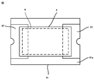
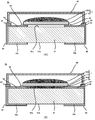
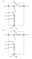
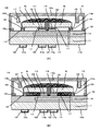
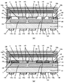
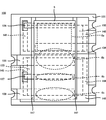
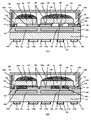
- FIG. 1 is a cross-sectional view of a fuse element to which the present invention is applied.
- FIG. 1A is a cross-sectional view illustrating a case where a flux sheet is provided on a fusible conductor, and FIG. It is sectional drawing explaining the case where it has a flux sheet under a soluble conductor, and FIG.1 (C) is sectional drawing explaining the case where it has a flux sheet on the soluble conductor upper and lower sides, respectively.
- FIG. 2 is a plan view of a fuse element to which the present invention is applied.
- 3A is a cross-sectional view showing an example of a flux sheet to which the present invention is applied
- FIG. 3B is a cross-sectional view showing a modification of the flux sheet
- FIG. 4A is a plan view showing a case where the flux sheet is elliptical as a modification of the fuse element to which the present invention is applied
- FIG. 4B is a diagram of the fuse element to which the present invention is applied.
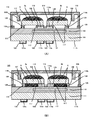
- FIG. 5 is a cross-sectional view showing a modification of the fuse element to which the present invention is applied
- FIG. 5 (A) is a cross-sectional view illustrating a case where an insulator piece-containing flux is applied onto a soluble conductor.
- FIG. 5B is a cross-sectional view illustrating the case where the insulator piece-containing flux is applied under the soluble conductor
- FIG. 5C is the insulator piece-containing flux applied above and below the soluble conductor. It is sectional drawing explaining the case where it did.
- FIG. 6 (A) is a plan view showing a case where an insulator piece-containing flux is applied in an elliptical shape as a modification of the fuse element to which the present invention is applied
- FIG. 6 (B) is a diagram in which the present invention is applied. It is a top view which shows the case where the insulator piece containing flux is apply
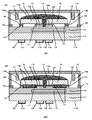
- FIG. 7 is a cross-sectional view showing a fuse element to which the present invention is applied.
- FIG. 7A is a cross-sectional view for explaining a case where a flux sheet is mounted on a soluble conductor, and FIG. However, it is sectional drawing explaining the case where a flux sheet is each mounted on a soluble conductor and under a soluble conductor.
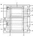
- FIG. 8 is a plan view showing the fuse element to which the present invention is applied, with the cover member removed.
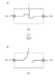
- FIG. 9 is a cross-sectional view showing a melted state of the fusible conductor of the fuse element to which the present invention is applied.
- FIG. 10A is a circuit diagram before the fusible conductor of the fuse element to which the present invention is applied, and FIG.
- FIG. 10B is the circuit diagram before the fusible conductor of the fuse element to which the present invention is applied.
- FIG. 11 is a cross-sectional view showing a modified example of the fuse element to which the present invention is applied, and FIG. 11A is a cross-sectional view for explaining a case where a flux sheet is mounted on a soluble conductor. It is sectional drawing explaining the case where (B) each mounts a flux sheet on a soluble conductor and under a soluble conductor.
- FIG. 12 is a cross-sectional view showing another modified example of the fuse element to which the present invention is applied, and FIG. 12A is a cross-sectional view illustrating a case where an insulating piece-containing flux is applied onto a soluble conductor FIG.
- FIG. 12B is a cross-sectional view illustrating the case where the insulator piece-containing flux is applied on the soluble conductor and below the soluble conductor, respectively.
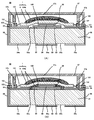
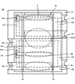
- FIG. 13 is a cross-sectional view of a protection element to which the present invention is applied.
- FIG. 13A is a cross-sectional view illustrating a case where a flux sheet is mounted on a soluble conductor, and FIG. It is sectional drawing explaining the case where a flux sheet is mounted on a soluble conductor and under a soluble conductor, respectively.
- FIG. 14A is a plan view showing the protection element to which the present invention is applied, with the cover member removed, and FIG. 14B is a view before the soluble conductor of the protection element to which the present invention is applied is blown out.
- FIG. FIG. 15 is a cross-sectional view showing a melted state of the soluble conductor of the protective element to which the present invention is applied.
- FIG. 16A is a plan view showing the protection element to which the present invention is applied in a state where the soluble conductor is melted and the cover member is removed, and
- FIG. 16B is a protection element to which the present invention is applied. It is a circuit diagram after a fusible conductor is blown out.
- FIG. 17 is a cross-sectional view showing a modification of the protection element to which the present invention is applied
- FIG. 17A is a cross-sectional view illustrating a case where a flux sheet is mounted on a soluble conductor.
- FIG. 18 is a cross-sectional view showing another modification of the protection element to which the present invention is applied
- FIG. 18A is a cross-sectional view for explaining the case where the insulator piece containing flux is applied onto the soluble conductor
- FIG. 18B is a cross-sectional view illustrating the case where the insulator piece-containing flux is applied on the soluble conductor and below the soluble conductor, respectively.
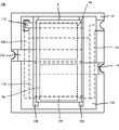
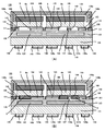
- FIG. 19 is a plan view showing the short-circuit element to which the present invention is applied with the cover member removed.
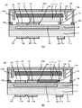
- FIG. 20 is a cross-sectional view of a short-circuit element to which the present invention is applied.
- FIG. 20A is a cross-sectional view illustrating a case where a flux sheet is mounted on a soluble conductor
- FIG. It is sectional drawing explaining the case where a flux sheet is mounted on a soluble conductor and under a soluble conductor, respectively.
- FIG. 21 is a cross-sectional view showing a melted state of the soluble conductor of the short-circuit element to which the present invention is applied.
- 22A is a circuit diagram before the soluble conductor of the short-circuit element to which the present invention is applied
- FIG. 22B is the circuit diagram before the soluble conductor of the short-circuit element to which the present invention is applied.
- FIG. 20A is a cross-sectional view illustrating a case where a flux sheet is mounted on a soluble conductor
- FIG. It is sectional drawing explaining the case where a flux sheet is mounted on a soluble
- FIG. 23 is a cross-sectional view showing a modification of the short-circuit element to which the present invention is applied
- FIG. 23 (A) is a cross-sectional view illustrating a case where a flux sheet is mounted on a soluble conductor. It is sectional drawing explaining the case where (B) each mounts a flux sheet on a soluble conductor and under a soluble conductor.
- FIG. 24 is a cross-sectional view showing another modification of the short-circuit element to which the present invention is applied
- FIG. 24A is a cross-sectional view for explaining the case where the insulator piece containing flux is applied onto the soluble conductor FIG.
- FIG. 24B is a cross-sectional view illustrating the case where the insulator piece-containing flux is applied on the soluble conductor and below the soluble conductor, respectively.
- FIG. 25 is a plan view showing another modification of the short-circuit element to which the present invention is applied.
- FIG. 26 is a cross-sectional view showing another modification of the short-circuit element to which the present invention is applied, and
- FIG. 26 (A) is a cross-sectional view illustrating a case where a flux sheet is mounted on a soluble conductor,
- FIG. 26B is a cross-sectional view illustrating a case where flux sheets are mounted on the soluble conductor and below the soluble conductor, respectively.
- FIG. 27 is a cross-sectional view showing another modification of the short-circuit element to which the present invention is applied
- FIG. 27A is a cross-sectional view illustrating a case where a flux sheet is mounted on two soluble conductors, respectively.
- FIG. 27B is a cross-sectional view illustrating a case where a flux sheet is mounted on two soluble conductors and below the two soluble conductors.
- FIG. 28 is a cross-sectional view showing another modification of the short-circuit element to which the present invention is applied
- FIG. 28 (A) is a cross-sectional view illustrating a case where a flux sheet is mounted on a soluble conductor, FIG.
- FIG. 28B is a cross-sectional view illustrating a case where flux sheets are mounted on the soluble conductor and below the soluble conductor, respectively.
- FIG. 29 is a cross-sectional view showing another modification of the short-circuit element to which the present invention is applied
- FIG. 29A is a cross-sectional view illustrating a case where a flux sheet is mounted on two soluble conductors, respectively.
- FIG. 29B is a cross-sectional view illustrating a case where a flux sheet is mounted on two soluble conductors and under two soluble conductors, respectively.
- FIG. 30 is a cross-sectional view showing another modification of the short-circuit element to which the present invention is applied, and FIG.
- FIG. 30A is a cross-sectional view for explaining the case where the insulator piece containing flux is applied onto the soluble conductor
- FIG. 30B is a cross-sectional view illustrating the case where the insulator piece-containing flux is applied on the soluble conductor and below the soluble conductor, respectively.
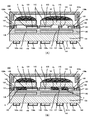
- FIG. 31 is a plan view showing the switching element to which the present invention is applied with the cover member removed.
- 32 is a cross-sectional view of a switching element to which the present invention is applied.
- FIG. 32A is a cross-sectional view illustrating a case where a flux sheet is mounted on a soluble conductor
- FIG. It is sectional drawing explaining the case where a flux sheet is mounted on a soluble conductor and under a soluble conductor, respectively.
- FIG. 33 is a circuit diagram before the fusible conductor of the switching element to which the present invention is applied is blown.
- FIG. 34 is a circuit diagram after the fusible conductor of the switching element to which the present invention is applied is blown.
- FIG. 35 is a cross-sectional view showing a melted state of the soluble conductor of the switching element to which the present invention is applied.
- FIG. 36 is a plan view showing the switching element to which the present invention is applied with the cover member removed, and is a view for explaining a state in which the second soluble conductor is melted earlier than the first soluble conductor.
- FIG. 37 is a plan view showing the switching element to which the present invention is applied with the cover member removed, and is a view for explaining a state where both the first soluble conductor and the second soluble conductor are melted.
- 38 is a cross-sectional view showing a modification of the switching element to which the present invention is applied, and FIG. 38 (A) is a cross-sectional view illustrating a case where a flux sheet is mounted on a soluble conductor. It is sectional drawing explaining the case where (B) each mounts a flux sheet on a soluble conductor and under a soluble conductor.
- FIG. 39 is a cross-sectional view showing another modified example of the switching element to which the present invention is applied.
- FIG. 39A shows a case where the insulator piece-containing flux is applied together on two soluble conductors. It is sectional drawing to explain, FIG.39 (B) is sectional drawing explaining the case where an insulator piece containing flux is apply
- FIG. 40 is a cross-sectional view showing another modification of the switching element to which the present invention is applied, and FIG. 40A explains a case where flux sheets are individually mounted on two soluble conductors.
- FIG. 40B is a cross-sectional view illustrating a case where flux sheets are individually mounted on two soluble conductors and under two soluble conductors, respectively.
- FIG. 41 is a cross-sectional view showing another modification of the switching element to which the present invention is applied, and FIG. 41 (A) explains a case where flux sheets are individually mounted on two soluble conductors.
- FIG. 41B is a cross-sectional view illustrating a case where flux sheets are individually mounted on two soluble conductors and below the two soluble conductors, respectively.
- FIG. 42 is a cross-sectional view showing another modification of the switching element to which the present invention is applied, and FIG. 42 (A) shows a case where an insulator piece-containing flux is individually applied onto two soluble conductors.
- FIG. 42B is a cross-sectional view illustrating the case where the insulator piece-containing flux is individually applied on two soluble conductors and below the two soluble conductors.
- the fuse element 1 to which the present invention is applied is also used for a fuse element, a protection element, a short-circuit element, and a switching element, which will be described later. It is blown by the heat of the body.
- the fuse element 1 is formed by laminating high melting point solder mainly composed of lead and three or more metal layers having different melting points. For example, in the case of a metal laminated body of three or more layers having different melting points, as shown in FIG. 1 (A), FIG. 1 (B), and FIG.
- the low melting point metal layer 3 having a low melting point and the flux sheet 5 are formed, for example, in a substantially rectangular plate shape as shown in FIG.
- the high melting point metal layer 2 and the low melting point metal layer 3 constitute a soluble conductor 6.
- the refractory metal layer 2 is preferably made of, for example, Ag, Cu, or an alloy mainly composed of Ag or Cu, and has a high melting point that does not melt even when the fuse element 1 is mounted on an insulating substrate by a reflow furnace. Have.
- the low melting point metal layer 3 is preferably made of, for example, a material generally called “Pb-free solder” made of Sn or an alloy containing Sn as a main component.
- the melting point of the low melting point metal layer 3 is not necessarily higher than the temperature of the reflow furnace, and may be melted at about 200 ° C.
- the fuse element 1 is formed by laminating three or more metal layers having different melting points, the fuse element 1 is excellent in mountability of the fuse element, the protective element, the short-circuit element, and the switching element on the insulating substrate. It is possible to improve the mountability of each element in which is used to an external circuit board. Moreover, the fuse element 1 can implement
- the fuse element 1 includes the refractory metal layer 2, so that fusing and deformation can be prevented even when exposed to a high heat environment above the melting point of the low melting point metal layer 3 by an external heat source such as a reflow furnace.
- an external heat source such as a reflow furnace.
- the fuse element 1 can efficiently realize mounting of each element such as a fuse element on an insulating substrate and mounting of each element such as a fuse element on an external circuit board by reflow mounting, thereby improving the mountability. Can be made.
- the fuse element 1 is formed by laminating the low-resistance refractory metal layer 2, the conductor resistance can be greatly reduced as compared with the fusible conductor using the conventional lead-based refractory solder. Out. Further, by laminating the low melting point metal layer 3 and the high melting point metal layer 2, the melting temperature of the fuse element 1 can be reduced to about 300 to 400 ° C., and it is composed of a dumbbell-shaped copper foil element having a melting point of 1085 ° C. Compared with a conventional chip fuse of the same size, the current rating can be greatly improved. In addition, it can be made thinner than conventional chip fuses having the same current rating, and is excellent in quick fusing.
- the fuse element 1 can be used to prevent the oxidation of the high melting point metal layer 2 or the low melting point metal layer 3 of the fusible conductor 6 and to remove the oxide at the time of fusing and improve the fluidity of the solder.
- a flux sheet 5 is mounted over the entire outermost layer of the molten conductor 6.
- the flux sheet 5 is mounted below the soluble conductor 6 as shown in FIG. 1B, that is, soluble, as shown in FIG. 1B, in addition to being mounted on the soluble conductor 6 as shown in FIG. You may comprise so that the lower surface of the conductor 6 may be contact
- the flux sheet 5 is mounted under the fusible conductor 6 and the fuse element 1 is connected downward to the substrate of each element, it is necessary to secure a margin for connection to the lower surface of the fusible conductor 6. is there. For this reason, it is preferable to make the flux sheet 5 smaller than the area of the lower surface of the soluble conductor 6, and the sheet body which opened the connection part may be sufficient.
- the flux sheet 5 is mounted on the soluble conductor 6 and below the soluble conductor 6 as shown in FIG. 1 (C), in addition to those described with reference to FIGS. 1 (A) and 1 (B). It may be.
- the flux sheets 5 By mounting the flux sheets 5 on the upper and lower sides of the soluble conductor 6, it is possible to expect more stable oxide removal and improved solder fluidity during fusing.
- the upper and lower sides of the soluble conductor 6 are the same as those described in FIGS. 1A and 1B, the description of the flux sheet 5 shown in FIG.
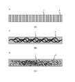
- the flux sheet 5 is obtained by impregnating and holding a fluid or semi-fluid flux 7 on a sheet-like support 8.
- the flux sheet 5 can hold a fluid or semi-fluid flux 7 by a support 8 having liquid retention.
- the support body 8 is used by mounting the flux sheet 5 on the soluble conductor 6 and / or below the soluble conductor 6, it influences electrical characteristics such as fusing of the soluble conductor 6.
- Insulator is used so that there is no.
- Various materials can be used as the material for forming the support 8 depending on its structure. For example, an insulator such as resin or glass is suitable.
- the flux sheet 5 is obtained by impregnating a porous support 8 with a flux 7 in FIG.
- the porous material may be a structure having a large number of holes penetrating in the vertical direction of the sheet as shown in FIG. 3A or a sponge-like structure. That is, the flux sheet 5 is made of a structure having a large number of voids such as a porous body and a sponge body, thereby improving the liquid retention, and the flux 7 is placed on the soluble conductor 6 and / or below the soluble conductor 6. It can be held in a desired position.
- the flux sheet 5 is obtained by impregnating the support 7, which is a nonwoven fabric or a mesh-like fabric, with the flux 7 in FIG. 3 (B).
- the fabric is a fibrous structure as shown in FIG. That is, the flux sheet 5 can improve the liquid retention by the fibrous structure and can hold the flux 7 at a desired position on the soluble conductor 6 and / or below the soluble conductor 6.
- the flux sheet 5 is formed by kneading the needle-like and short fiber-like support 8 with the flux 7 in FIG.
- the needle shape and the short fiber shape will be described in detail in the description of the flux described later.
- the flux sheet 5 has a needle-like and short fiber-like structure to improve liquid retention, and the flux 7 can be held at a desired position on the soluble conductor 6 and / or below the soluble conductor 6.
- the support 8 can use various insulators that retain the flux 7 and have liquid retainability, but at least up to the mounting temperature of the fuse element 1 and each element using the same, a soluble conductor. It is necessary to hold the flux 7 on 6. Accordingly, the support 8 needs to have heat resistance enough to maintain its shape, and is deformed or melted at a temperature exceeding the mounting temperature of the fuse element 1 or each element using the fuse element 1 and has fluidity. Can be used. That is, at the temperature at which the fusible conductor 6 is blown so as to exceed the mounting temperature, it is no longer necessary to hold the flux 7 on the fusible conductor 6, so that the support 8 melts and flows together with the flux 7. . Since the support 8 has melting or fluidity, the support 8 is not left behind when the soluble conductor 6 is melted, and the insulating characteristics can be improved.
- the support 8 is preferably made of a material that is deformed or melted at a temperature of 300 ° C. or higher and has fluidity.
- the support 8 preferably has a specific gravity equal to or lower than that of the soluble conductor 6. This is because when the fusible conductor 6 is melted, the support 8 needs to be lightened in order to gather the molten conductor. That is, if the specific gravity of the support body 8 is greater than that of the soluble conductor 6, the support body 8 presses the molten conductor, so that the molten conductor is less likely to be collected and the fusing characteristics of the fuse element 1 may be deteriorated. Because.
- the specific gravity of the support 8 is preferably not more than the specific gravity of the low melting point metal layer 3, and more specifically the specific gravity is It is preferable to use a material of 5 g / cm 3 or less.
- the flux sheet 5 has an area larger than the surface area of the soluble conductor 6 as shown in FIG. Thereby, even when the soluble conductor 6 is completely covered by the flux sheet 5 and the volume expands due to melting, it is possible to surely realize the rapid fusing by removing the oxidation by the flux 7 and improving the wettability. . Further, as shown in FIGS. 1B and 1C, the flux sheet 5 has an area smaller than the surface area of the soluble conductor 6 when mounted on the lower surface of the soluble conductor 6. Thereby, the fusible conductor 6 is covered with the flux sheet 5 and the margin of connection of each element to the substrate can be secured.
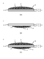
- the flux sheet 5 may have a circular or elliptical shape as shown in FIGS. 4 (A) and 4 (B). Such a flux sheet 5 can obtain a circular or elliptical shape, for example, by punching a sheet sufficiently larger than the surface area of the soluble conductor 6.
- the diameter of the circle or ellipse is preferably larger than the short side of the rectangular soluble conductor 6.
- the position where the flux sheet 5 is mounted is a position where the center of a circle or an ellipse overlaps the melted portion of the soluble conductor 6.
- the flux sheet 5 By mounting the flux sheet 5 on the fusible conductor 6 and / or below the fusible conductor 6, it is possible to hold the flux over the entire surface of the fusible conductor 6 even in the heat treatment process when mounting the fuse element 1. While improving the wettability of the low-melting-point metal layer 3 (for example, solder) of the molten conductor 6, the oxide is removed while the low-melting-point metal layer 3 is dissolved, and the erosion action to the high-melting-point metal (for example, Ag) It can be used to improve the fast fusing property.
- the low-melting-point metal layer 3 for example, solder
- the surface of the outermost refractory metal layer 2 of the soluble conductor 6 is Pb-free containing Sn as a main component. Even when an anti-oxidation film such as solder is formed, the oxide of the anti-oxidation film can be removed, the oxidation of the refractory metal layer 2 can be effectively prevented, and the fast fusing property can be maintained and improved. Can do.
- the sheet-like support 8 is not impregnated with the fluid or semi-fluid flux 7, and the fluid or semi-fluid flux 7 is needle-like or You may make it apply
- the insulator piece-containing flux 9 is composed of a fluid or semi-fluid flux 7 and needle-like or short fiber insulator pieces 10.
- the same flux as the above-described flux impregnated in the flux sheet 5 can be used.
- the insulator piece 10 is a needle-like or short fiber insulator.
- the insulator pieces 10 have individual lengths that do not affect the fluidity of the flux 7 and are entangled with each other when mixed with the flux 7 or hold the flux 7 between each other by surface tension. A structure having a predetermined surface area is provided.
- the shape of the insulator piece 10 is not limited to a needle shape or a short fiber, and may be, for example, a structure having a hook-like structure and entangled with each other by the hook-like structure.
- the insulator piece 10 is not limited to a single shape, and may have different shapes and lengths.
- the insulator piece-containing flux 9 is applied below the soluble conductor 6 as shown in FIG. 5 (B). You may comprise so that it may apply
- FIG. 5 (B) when the insulator piece containing flux 9 is applied under the fusible conductor 6 and the fuse element 1 is connected downward to the substrate of each element, a margin is secured for the lower surface of the fusible conductor 6. There is a need to. For this reason, it is preferable to apply the insulator piece-containing flux 9 to be smaller than the area of the lower surface of the fusible conductor 6, and it is preferable to apply it while avoiding the connection portion.
- the insulator piece-containing flux 9 is provided on the soluble conductor 6 and below the soluble conductor 6 as shown in FIG. 5C, in addition to those described with reference to FIGS. 5A and 5B. You may make it apply
- the insulator piece-containing flux 9 By applying the insulator piece-containing flux 9 above and below the soluble conductor 6, it is possible to expect more stable oxide removal and improved solder fluidity during melting. Note that the insulator piece-containing flux 9 shown in FIG. 5C is the same as that described above with reference to FIGS.
- the insulator piece-containing flux 9 containing the insulator piece 10 described above is applied to the fusible conductor 6 in a circular or elliptical shape, thereby providing a flux sheet.
- 5 can hold the flux 7 equivalent to 5, and can simplify the sheet creation and sheet mounting process compared to the flux sheet 5 and change the manufacturing process for applying flux to the former soluble conductor This can be done without
- the insulator piece-containing flux 9 is applied in a rectangular shape over the entire surface of the soluble conductor 6 and / or the lower surface of the soluble conductor 6 from the viewpoint of removing the oxide during melting and improving the fluidity of the solder. Is more preferable. However, it is necessary to leave a connection margin without applying the insulating piece-containing flux 9 to the connection portion to each element under the soluble conductor 6 as shown in FIGS. Needless to say, this is the same as the case described in (C).
- the fuse element 1 is an electric system in which each element such as a fuse element is incorporated by forming the inner layer provided between the pair of refractory metal layers 2 as the low melting point metal layer 3 and the outer layer as the refractory metal layer 2.
- a surge pulse resistance
- the fuse element 1 must not be blown until the fusible conductor 6 has a current of, for example, 100 A flowing for several milliseconds.
- the fuse element 1 since a large current flowing in a very short time flows in the surface layer of the conductor (skin effect), the fuse element 1 is provided with a refractory metal layer 2 such as Ag plating having a low resistance value as the outer layer of the soluble conductor 6. Therefore, it is easy to flow the current applied by the surge, and the fusing due to self-heating can be prevented. Therefore, the fuse element 1 can greatly improve the resistance to a surge as compared with a fuse made of a conventional solder alloy.
- the volume of the low melting point metal layer 3 of the fusible conductor 6 is preferably larger than the volume of the high melting point metal layer 2.
- the fuse element 1 can be effectively blown in a short time by erosion of the high melting point metal layer 2.
- the fuse element 1 forms a soluble conductor 6 by forming a high melting point metal 2 on the surface of the low melting point metal layer 3 using a plating technique, and forms a flux on the soluble conductor 6 and / or below the soluble conductor 6. It can be manufactured by mounting the sheet 5.
- the soluble conductor 6 can be efficiently manufactured by, for example, applying Ag plating to the surface of a long solder foil, and can be easily used by cutting according to the size at the time of use.
- the soluble conductor 6 may be manufactured by laminating a low melting point metal foil constituting the low melting point metal layer 3 and a high melting point metal foil constituting the high melting point metal layer 2.
- the fusible conductor 6 can be produced by, for example, sandwiching and pressing a solder foil constituting the rolled low melting point metal layer 3 between two rolled Cu foils or Ag foils.
- the low melting point metal foil it is preferable to select a softer material than the high melting point metal foil.
- variation in thickness can be absorbed and a low melting metal foil and a high melting metal foil can be stuck without gap.
- the film thickness of the low melting point metal foil is reduced by pressing, it is preferable to make it thick beforehand.
- the low-melting-point metal foil protrudes from the end face of the soluble conductor by pressing, it is preferable to trim off and adjust the shape.
- the fusible conductor 6 forms the fusible conductor 6 in which the low melting point metal layer 3 and the high melting point metal layer 2 are laminated by using a thin film forming technique such as vapor deposition or other well-known lamination technique. can do.
- the soluble conductor 6 may further include an antioxidant film (not shown) on the surface of the outermost refractory metal layer 2 when one refractory metal layer 2 is the outermost layer.
- the fusible conductor 6 prevents the oxidation of Cu even when, for example, Cu plating or Cu foil is formed as the refractory metal layer 2 by coating the outermost refractory metal layer 2 with an antioxidant film. can do. Therefore, the soluble conductor 6 can prevent the situation where the fusing time is prolonged due to the oxidation of Cu, and can be fused in a short time.
- the soluble conductor 6 can be made of an inexpensive but easily oxidized metal such as Cu as the high melting point metal layer 2 and can be formed without using an expensive material such as Ag.
- the high melting point metal antioxidant film can be made of the same material as the low melting point metal layer 3, for example, Pb-free solder containing Sn as a main component.
- the antioxidant film can be formed by performing tin plating on the surface of the refractory metal layer 2.
- the antioxidant film can be formed by Au plating or preflux.
- the flux sheet 5 is prepared by impregnating the support 7 having a sufficiently larger area than the soluble conductor 6 with the flux 7 and heating it with an oven or the like to dry and solidify the solvent content of the flux 7. And it can produce by cut
- the flux sheet 5 can also be created directly without creating a mother sheet. In this case, the cutting process of the flux sheet 5 can be omitted.
- the cut out flux sheet 5 is mounted on the soluble conductor 6 so as to completely cover the soluble conductor 6.
- a small amount of liquid flux 7 is dropped or applied as a fixing agent for temporarily fixing the flux sheet 5 on the soluble conductor 6, and the flux sheet 5 is placed and dried, whereby the flux sheet 5 is placed on the soluble conductor 6.
- the flux sheet 5 is mounted under the soluble conductor 6, the flux sheet 5 smaller than the surface area of the lower surface of the soluble conductor 6 is mounted with the lower surface of the soluble conductor 6 facing upward.
- a small amount of liquid flux 7 is dropped or applied as a fixing agent for temporarily fixing the flux sheet 5 under the soluble conductor 6 and the flux sheet 5 is placed and dried, so that the flux sheet 5 is placed under the soluble conductor 6. Can be installed.
- the flux sheet 5 when mounting the flux sheet 5 on the soluble conductor 6 and below the soluble conductor 6, the flux sheet 5 may be mounted on each side of the soluble conductor 6.
- One or both of 5 may be temporarily fixed, and the fixing agent may be dried by heating when bonding a cover member of each element described later.
- a support body 8 corresponding to the size of the flux sheet 5 is cut out from a mother support body sufficiently larger than the area of the soluble conductor 6.
- the cut support body 8 is placed before the flux 7 is dried. Since the support 8 has liquid retention, the support 8 absorbs the flux 7 and is integrated with the flux 7.
- the flux sheet 5 is formed by drying and solidifying the solvent content of the flux 7 through a drying process.
- the support 8 cut out smaller than the surface area of the lower surface of the soluble conductor 6 is placed. Since the support 8 has liquid retention, the support 8 absorbs the flux 7 and is integrated with the flux 7. Then, the flux sheet 5 is formed on the lower surface of the soluble conductor 6 by drying and solidifying the solvent of the flux 7 through a drying process.
- the process of manufacturing the flux sheet 5 in advance can be omitted, and the fuse element 1 can be manufactured simply by placing the support 8 after the normal application process of the flux 7. No complicated manufacturing process is required.
- the flux sheet 5 is not mounted on the soluble conductor 6, that is, a case in which the insulator piece containing flux 9 is used will be described.
- an insulating piece-containing flux 9 having fluidity or semi-fluidity is applied or dropped, and the insulating piece-containing flux 9 spreads on the fusible conductor 6. Equivalent configurations and effects can be obtained.
- the insulator piece-containing flux 9 is applied to the lower surface of the soluble conductor 6 with the lower surface of the soluble conductor 6 facing upward.
- the process of manufacturing the flux sheet 5 in advance can be omitted, and the fuse element can be simply obtained by applying the insulator piece-containing flux 9 using the same process as the application process of the normal flux 7. 1 can be manufactured, and a complicated manufacturing process is not required.
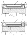
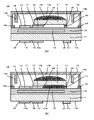
- a fuse element 80 to which the present invention is applied includes an insulating substrate 81, a first electrode 82 and a second electrode 83 provided on the insulating substrate 81, and first and second electrodes.
- a fuse element 1 mounted between the two electrodes 82 and 83, which is blown by self-heating when a current exceeding the rating is applied, and interrupts the current path between the first electrode 82 and the second electrode 83;
- a cover member 89 that covers the fuse element 1 on the insulating substrate 81.
- the fuse element 1 includes a fusible conductor 6 and a flux sheet 5 mounted on and / or under the fusible conductor 6.
- the insulating substrate 81 is formed in a square shape by an insulating member such as alumina, glass ceramics, mullite, zirconia, for example.
- the insulating substrate 81 may be made of a material used for a printed wiring board such as a glass epoxy board or a phenol board.
- First and second electrodes 82 and 83 are formed on opposite ends of the insulating substrate 81.
- the first and second electrodes 82 and 83 are each formed by a conductive pattern such as Ag or Cu wiring, and Sn plating, Ni / Au plating, Ni / Pd plating, Ni / Pd are appropriately applied to the surface as anti-oxidation measures.
- a protective layer 86 such as / Au plating is provided.
- the first and second electrodes 82 and 83 are continued from the front surface 81a of the insulating substrate 81 to the first and second external connection electrodes 82a and 83a formed on the back surface 81b through castellation. .
- the fuse element 80 is mounted on the current path of the circuit board via the first and second external connection electrodes 82a and 83a formed on the back surface 81b.
- the fusible conductor 6 of the fuse element 1 is connected to the first and second electrodes 82 and 83 via a connecting material 88 such as solder.
- a connecting material 88 such as solder.
- the fuse element 1 has excellent mountability because the fusible conductor 6 includes the refractory metal layer 2 and has improved resistance to a high temperature environment. Can be easily connected by reflow soldering or the like.
- the fuse element 80 is formed of a soluble conductor to prevent oxidation of the high melting point metal layer 2 or the low melting point metal layer 3 and to remove oxide at the time of melting and to improve solder fluidity.
- the flux sheet 5 over the entire surface of the outermost layer on 6 is mounted.
- seat 5 since what is substantially equivalent to what was demonstrated by the fuse element 1 mentioned above is used, illustration and illustration are abbreviate
- mounting the flux sheet 5 under the fusible conductor 6 is applicable to the case described in the fuse element 1 described above as shown in FIG. Only an example in which the flux sheet 5 is mounted will be described, and detailed illustration and description will be omitted. The same applies to all the following embodiments.
- the flux sheet 5 is obtained by impregnating and holding a fluid-like or semi-fluid flux 7 in a sheet-like support 8, for example, a nonwoven fabric or mesh-like fabric impregnated with the flux 7, or a soluble material.
- a non-woven fabric or mesh-like cloth is placed on the flux 7 applied to the outermost layer of the conductor 6 and impregnated with the flux 7.
- the flux sheet 5 preferably has an area larger than the surface area of the soluble conductor 6. Thereby, even when the soluble conductor 6 is completely covered by the flux sheet 5 and the volume expands due to melting, it is possible to surely realize the rapid fusing by removing the oxidation by the flux 7 and improving the wettability. .
- the flux 7 can be held over the entire surface of the fusible conductor 6 in the heat treatment process when the fuse element 1 or the fuse element 80 is mounted.
- the low melting point metal layer 3 for example, solder
- the oxide while the first and second low melting point metals are dissolved is removed.
- the fast fusing property can be improved by using the erosion action on Ag).
- an antioxidant film such as Pb-free solder containing Sn as a main component is formed on the surface of the refractory metal layer 2 that is the outermost layer of the soluble conductor 6.
- the oxide of the antioxidant film can be removed, the refractory metal layer 2 can be effectively prevented from being oxidized, and the fast fusing property can be maintained and improved.
- a cover member 89 that protects the inside and prevents the molten fuse element 1 from scattering is attached to the surface 81 a of the insulating substrate 81 on which the fuse element 1 is provided.
- the cover member 89 can be formed of an insulating member such as various engineering plastics and ceramics.
- the fuse element 80 since the fuse element 1 is covered by the cover member 89, the molten metal is captured by the cover member 89 and can be prevented from being scattered to the surroundings even when the self-heating is interrupted due to the occurrence of arc discharge due to overcurrent. .
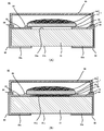
- the cover member 89 has a protrusion 89b extending from the top surface 89a toward the insulating substrate 81 to at least the side surface of the flux sheet 5.
- the side surface of the flux sheet 5 is subjected to movement restriction by the protrusion 89b, so that it is possible to prevent the positional deviation of the flux sheet 5.
- the protrusion 89b is provided in a size that holds a predetermined clearance rather than the size of the flux sheet 5, and is provided corresponding to the position where the flux sheet 5 should be held.
- the protrusion part 89b is good also as a wall surface which wraps around the side surface of the flux sheet 5, and may protrude partially.
- the cover member 89 is configured to have a predetermined interval between the flux sheet 5 and the top surface 89a. This is because, as shown in FIG. 9, when the soluble conductor 6 is melted, a clearance is required for the molten molten conductor to push up the flux sheet 5.
- the cover member 89 has a height of the internal space of the cover member 89 (height up to the top surface 89a) that is the height of the melted soluble conductor 6 on the surface 81a of the insulating substrate 81 (a plurality of molten conductors). When divided, the height of the molten conductor is the highest) and the thickness of the flux sheet 5 is greater than the sum.
- the molten metal of the fusible conductor is between the first and second electrodes. Leakage occurs on the top.
- a fusible conductor is formed by printing an Ag paste on a ceramic substrate
- the ceramic and Ag are sintered and bite into the fuse element, and remain between the first and second electrodes. Therefore, a leak current flows between the first and second electrodes due to the residue, and the current path cannot be completely blocked.
- the fusible conductor 6 is formed separately from the insulating substrate 81, and is mounted away from the surface 81a of the insulating substrate 81. Therefore, the fuse element 80 is drawn onto the first and second electrodes 82 and 83 without the molten metal biting into the insulating substrate 81 even when the fusible conductor 6 is melted. 82 and 83 can be insulated.
- the fuse element 80 can connect the fusible conductor 6 to the first and second electrodes 82 and 83 by reflow soldering as described above.
- the conductor 6 may be connected to the first and second electrodes 82 and 83 by ultrasonic welding.
- the fuse element 80 is mounted on the fusible conductor 6 so that the flux sheet 5 completely covers the fusible conductor 6.
- the flux sheet 5 is fixed on the soluble conductor 6 by dropping or applying a small amount of liquid flux 7 as a fixing agent to be temporarily fixed on the soluble conductor 6 and placing the flux sheet 5 thereon.
- the cover member 89 is bonded onto the insulating substrate 81 via the adhesive 84. Since the projection 89b of the cover member 89 has a predetermined clearance with respect to the mounting position of the flux sheet 5, it does not interfere with the flux sheet 5.
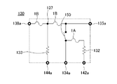
- Such a fuse element 80 has a circuit configuration shown in FIG.
- the fuse element 80 is incorporated in the current path of the external circuit by being mounted on the external circuit via the first and second external connection electrodes 82a and 83a.
- the fuse element 80 is not melted by self-heating while a predetermined rated current flows through the fusible conductor 6.
- the fuse element 80 is melted by the self-heating of the fusible conductor 6, and the first and second electrodes 82 and 83 are cut off, so that the current path of the external circuit is reduced. Shut off (FIG. 10B).
- the fuse element 80 since the fuse element 80 has the low melting point metal layer 3 having the melting point lower than that of the high melting point metal layer 2 as described above, the fusible conductor 6 is laminated with the high melting point metal by self-heating due to overcurrent. Begin to erode layer 2. Therefore, the fuse element 80 uses the erosion action of the high melting point metal layer 2 by the low melting point metal layer 3 of the fusible conductor 6, so that the high melting point metal layer 2 is melted at a temperature lower than the melting temperature and quickly. Can be melted.
- the molten metal of the fusible conductor 6 is divided into left and right by the physical pulling action of the first and second electrodes 82 and 83, so that it can be performed quickly and reliably.
- the current path between the first and second electrodes 82 and 83 can be cut off.
- the first and second electrodes 82 and 83 are respectively patterned on both opposite ends of the insulating substrate 81 by screen printing or the like on Ag, Cu wiring, etc.
- a base portion is manufactured by forming a protective layer 86 of Sn, Ni / Au, Ni / Pd, Ni / Pd / Au, etc. by plating.
- connection material 88 such as solder paste is applied on the first and second electrodes 82 and 83, and the fuse element 1 is spread over the first and second electrodes 82 and 83. Connect 6 soluble conductors. As a result, the fuse element 1, that is, the fusible conductor 6 is mounted on the first and second electrodes 82 and 83.
- the cover member 89 is adhered, thereby covering the fuse element 1 and completing the fuse element 80.
- the manufacturing process of the fuse element 1 may be divided into the manufacturing process of the fuse element 80.
- the fusible conductor 6 alone is 1.
- the flux sheet 5 is temporarily fixed on the soluble conductor 6 using a fixing agent such as flux 7, or the soluble conductor 6 alone May be applied on the first and second electrodes 82 and 83, and then the insulating piece-containing flux 9 may be applied.
- the adhesive 84 can be cured and the flux sheet 5 can be fixed.
- the fuse element 80 may be one obtained by replacing the flux sheet 5 with a flux sheet 85a.
- the fuse element 80 shown in FIG. 11 (A) there is no particular change in parts other than the flux sheet 85a.
- the flux sheet 85a is obtained by impregnating and holding a fluid-like or semi-fluid flux 7 on a sheet-like support 8 and, for example, a nonwoven fabric or mesh-like fabric impregnated with the flux 7, or a soluble material. A non-woven fabric or mesh-like cloth is placed on the flux 7 applied to the outermost layer of the conductor 6 and impregnated with the flux 7.
- the flux sheet 85a can hold the fluid or semi-fluid flux 7 by the support 8 having liquid retention.
- the soluble conductor 6 alone is mounted and connected on the first and second electrodes 82 and 83. Later, a fluid or semi-fluid flux 7 is applied or dropped onto the soluble conductor 6, and the sheet-like support 8 is placed on the flux 7.
- the flux sheet 85a can be mounted under the soluble conductor 6 as shown in FIG. Needless to say, the flux sheet 85 a may be mounted only under the soluble conductor 6.
- the fuse element 80 may be formed by replacing the flux sheet 5 with an insulator piece containing flux 85b.
- the fuse element 80 shown in FIG. 12A is not particularly changed with respect to portions other than the insulator piece-containing flux 85b.
- the insulator piece-containing flux 85b does not impregnate the sheet-like support 8 with the fluid or semi-fluid flux 7, and the needle or short fiber insulator piece 10 is added to the fluid or semi-fluid flux 7. Is kneaded and contained and applied to the soluble conductor 6.
- the insulator piece-containing flux 85b can hold the fluid or semi-fluid flux 7 on the soluble conductor 6 by the insulator piece 10 having liquid retention.
- the soluble conductor 6 alone is mounted on and connected to the first and second electrodes 82 and 83 in the method for manufacturing the fuse element 80 described above. Later, it can be manufactured by applying an insulator piece-containing flux 9 in which needle-like or short fiber insulator pieces 10 are mixed and contained on the soluble conductor 6.
- the insulator piece-containing flux 85b can be applied under the soluble conductor 6 as shown in FIG. Needless to say, the insulator piece-containing flux 85b may be applied only under the soluble conductor 6.
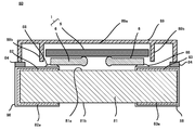
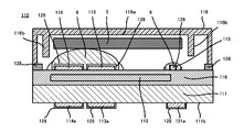
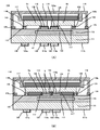
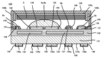
- a protection element 90 to which the present invention is applied includes an insulating substrate 91, a heating element 93 laminated on the insulating substrate 91, and covered with an insulating member 92.
- the first electrode 94 and the second electrode 95 formed on both ends of the insulating substrate 91 are stacked on the insulating substrate 91 so as to overlap the heating element 93 and are electrically connected to the heating element 93.
- a fuse element 1 having both ends connected to the first and second electrodes 94 and 95 and a center portion connected to the heating element lead electrode 96, and the fuse element 1 is covered on the insulating substrate 91.
- a cover member 97 The fuse element 1 includes a fusible conductor 6 and a flux sheet 5 mounted on and / or under the fusible conductor 6. The flux sheet 5 mounted under the soluble conductor 6 is illustrated in FIG.
- the insulating substrate 91 is formed in a rectangular shape by an insulating member such as alumina, glass ceramics, mullite, zirconia, and the like, similarly to the insulating substrate 81.
- the insulating substrate 91 may be made of a material used for a printed wiring board such as a glass epoxy board or a phenol board.
- First and second electrodes 94 and 95 are formed on opposite ends of the insulating substrate 91.
- the first and second electrodes 94 and 95 are each formed of a conductive pattern such as Ag or Cu wiring.
- the first and second electrodes 94 and 95 are continued from the front surface 91a of the insulating substrate 91 to the first and second external connection electrodes 94a and 95a formed on the back surface 91b through castellation.
- the protection element 90 is formed on the circuit board by connecting the first and second external connection electrodes 94b and 95b formed on the back surface 91b to connection electrodes provided on the circuit board on which the protection element 90 is mounted. It is incorporated into a part of the formed current path.
- the heating element 93 is a conductive member that generates heat when energized, and is made of, for example, nichrome, W, Mo, Ru, or a material containing these.
- the heating element 93 is a paste obtained by mixing powders of these alloys, compositions, or compounds with a resin binder or the like, and forming a pattern on the insulating substrate 91 using a screen printing technique, followed by firing. Etc. can be formed.
- the heating element 93 is covered with the insulating member 92, and the heating element extraction electrode 96 is formed so as to face the heating element 93 through the insulating member 92.
- the heating element lead electrode 96 is connected to the fusible conductor 6 of the fuse element 1, whereby the heating element 93 is superimposed on the fusible conductor 6 via the insulating member 92 and the heating element lead electrode 96.
- the insulating member 92 is provided to protect and insulate the heating element 93 and efficiently transmit the heat of the heating element 93 to the fusible conductor 6, and is made of, for example, a glass layer.
- the heating element 93 may be formed inside the insulating member 92 stacked on the insulating substrate 91.
- the heating element 93 may be formed on the back surface 91b of the insulating substrate 91 opposite to the surface on which the first and second electrodes 94 and 95 are formed.
- the heating element 93 may be formed on the surface 91a of the insulating substrate 91.
- the second electrodes 94 and 95 may be formed adjacent to each other. Further, the heating element 93 may be formed inside the insulating substrate 91.
- the heating element 93 has one end connected to the heating element extraction electrode 96 and the other end connected to the heating element electrode 99.
- the heating element extraction electrode 96 is formed on the surface 91 a of the insulating substrate 91 and is laminated on the insulating member 92 so as to face the heating element 93 and is connected to the heating element 93, and the fuse element 1. And an upper layer portion 96b connected to the soluble conductor 6.
- the heating element 93 is electrically connected to the fusible conductor 6 of the fuse element 1 via the heating element extraction electrode 96.
- the heating element extraction electrode 96 is disposed to face the heating element 93 with the insulating member 92 interposed therebetween, whereby the soluble conductor 6 can be melted and the molten conductor can be easily aggregated.
- the heating element electrode 99 is formed on the front surface 91a of the insulating substrate 91, and is continuous with the heating element feeding electrode 99a formed on the back surface 91b of the insulating substrate 91 through castellation.
- the protective element 90 is connected to the fusible conductor 6 of the fuse element 1 across the second electrode 95 from the first electrode 94 via the heating element extraction electrode 96.
- the fusible conductor 6 can be easily connected by reflow soldering or the like after being mounted on the first and second electrodes 94 and 95 and the heating element lead electrode 96 via a connecting material 100 such as solder. .
- the fuse element 1 has excellent mountability because the fusible conductor 6 includes the refractory metal layer 2 and thus has high resistance to high-temperature environments, and is excellent in mountability. Can be easily connected by reflow soldering or the like.
- the first and second electrodes 94 and 95, the heating element extraction electrode 96, and the heating element electrode 99 are formed of a conductive pattern such as Ag or Cu, and the surface thereof is appropriately Sn-plated, Ni / Au plated, Ni A protective layer 98 such as / Pd plating or Ni / Pd / Au plating is formed.
- the surface is prevented from being oxidized, and the first and second electrodes 94 and 95 and the heating element are drawn by the connection material 100 such as the low melting point metal layer 3 of the soluble conductor 6 and the solder for connecting the soluble conductor 6.
- the erosion of the electrode 96 can be suppressed.
- first and second electrodes 94 and 95 are formed with an outflow prevention portion 102 made of an insulating material such as glass that prevents the molten conductor of the fusible conductor 6 and the connection material 100 of the fuse element 1 from flowing out. Has been.
- the protective element 90 constitutes a part of the energization path to the heating element 93 by connecting the soluble conductor 6 to the heating element extraction electrode 96. Therefore, when the fusible conductor 6 is melted and the connection with the external circuit is interrupted, the protective element 90 can also stop the heat generation because the energization path to the heating element 93 is also interrupted.
- the protective element 90 can be used to prevent oxidation of the refractory metal layer 2 or the low melting point metal layer 3, to remove oxide during fusing, and to improve solder fluidity.
- a flux sheet 5 is mounted on the entire surface of the outermost layer on the molten conductor 6. The flux sheet 5 is obtained by impregnating and holding a fluid or semi-fluid flux 7 in a sheet-like support 8, for example, a nonwoven fabric or a mesh-like fabric impregnated with the flux 7.
- the flux sheet 5 preferably has an area larger than the surface area of the soluble conductor 6. Thereby, even when the soluble conductor 6 is completely covered with the flux sheet 5 and the volume expands due to melting, it is possible to reliably realize oxide removal by the flux 7 and quick fusing by improving wettability. it can.
- the flux 7 By disposing the flux sheet 5, the flux 7 can be held over the entire surface of the fusible conductor 6 even in the heat treatment process when the fuse element 1 is mounted or when the protective element 90 is mounted. 2, the wettability of the low-melting-point metal layer 3 (for example, solder) is enhanced, and the oxide while the first and second low-melting-point metals are dissolved is removed to erode the high-melting-point metal (for example, Ag). The fast fusing property can be improved by using the action.
- the low-melting-point metal layer 3 for example, solder
- an anti-oxidation film such as Pb-free solder mainly composed of Sn is formed on the surface of the outermost refractory metal layer 2 by arranging the flux sheet 5, the oxidation of the anti-oxidation film is also performed.
- the material can be removed, the refractory metal layer 2 can be effectively prevented from being oxidized, and the fast fusing property can be maintained and improved.
- the flux sheet 5 can be mounted under the soluble conductor 6. Needless to say, the flux sheet 5 may be mounted only under the soluble conductor 6.
- a cover member 97 that protects the inside and prevents the molten fuse element 1 from scattering is attached to the surface 91 a of the insulating substrate 91 on which the fuse element 1 is provided.
- the cover member 97 can be formed of an insulating member such as various engineering plastics and ceramics. Since the fuse element 1 is covered by the cover member 97, the fuse element 90 can prevent the molten metal from being scattered around by being caught by the cover member 97 even when self-heating is interrupted due to occurrence of arc discharge due to overcurrent. .
- the cover member 97 has a protruding portion 97b extending from the top surface 97a toward the insulating substrate 81 at least to the side surface of the flux sheet 5.
- the cover member 97 can prevent the positional deviation of the flux sheet 5 because the side surface of the flux sheet 5 is restricted by the protrusion 97b. That is, the protrusion 97b is provided in a size that holds a predetermined clearance rather than the size of the flux sheet 5, and is provided corresponding to the position where the flux sheet 5 should be held.
- the protrusion part 97b is good also as a wall surface which wraps around the side surface of the flux sheet 5, and may protrude partially.
- the cover member 97 is configured to have a predetermined gap between the flux sheet 5 and the top surface 97a. This is because, as shown in FIG. 15, when the soluble conductor 6 is melted, a clearance is required for the melted molten conductor to push up the flux sheet 5.
- the cover member 97 has the height of the internal space of the cover member 97 (the height to the top surface 97a) equal to the height of the meltable soluble conductor 6 on the surface 91a of the insulating substrate 91 (a plurality of molten conductors). When divided, the height of the molten conductor is the highest) and the thickness of the flux sheet 5 is greater than the sum.
- the molten metal of the fusible conductor is between the first and second electrodes. Leakage occurs on the top.
- a fusible conductor is formed by printing an Ag paste on a ceramic substrate
- the ceramic and Ag are sintered and bite into the fuse element, and remain between the first and second electrodes. Therefore, a leak current flows between the first and second electrodes due to the residue, and the current path cannot be completely blocked.
- the fusible conductor 6 is formed separately from the insulating substrate 91, and is mounted away from the surface 91a of the insulating substrate 91. Therefore, even when the fusible conductor 6 is melted, the fuse element 90 is drawn onto the first and second electrodes 94 and 95 and the heating element lead-out electrode 96 without the molten metal biting into the insulating substrate 91, so that the first The first and second electrodes 94 and 95 can be insulated from each other.
- the fuse element 1 can connect the fusible conductor 6 on the first and second electrodes 94 and 95 and the heating element lead electrode 96 by reflow soldering as described above.
- the fusible conductor 6 may be connected to the first and second electrodes 94 and 95 and the heating element extraction electrode 96 by ultrasonic welding.
- the fuse element 90 is mounted on the fusible conductor 6 so that the flux sheet 5 completely covers the fusible conductor 6.
- the flux sheet 5 is fixed on the soluble conductor 6 by dropping or applying a small amount of liquid flux 7 as a fixing agent to be temporarily fixed on the soluble conductor 6 and placing the flux sheet 5 thereon.
- the cover member 97 is bonded onto the insulating substrate 91 via the adhesive 103. Since the protrusion 97b of the cover member 97 has a predetermined clearance with respect to the mounting position of the flux sheet 5, it does not interfere with the flux sheet 5.
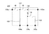
- the protective element 90 to which the present invention is applied has a circuit configuration as shown in FIG. That is, the protection element 90 includes the fusible conductor 6 connected in series across the first and second external connection terminals 94a and 95a via the heating element lead electrode 96, and the heating element serving as a connection point of the fusible conductor 6.
- the circuit configuration includes a heating element 93 that melts the soluble conductor 6 by energizing and generating heat through the extraction electrode 96.
- the first and second electrodes 94 and 95 and the heating element electrode 99 are connected to the first and second external connection terminals 94a and 95a and the heating element feeding terminal 99a, respectively, to the external circuit board.
- the fusible conductor 6 of the fuse element 1 is connected in series on the current path of the external circuit via the first and second electrodes 94 and 95, and the heating element 93 connects the heating element electrode 99. And is connected to a current control element provided in an external circuit.
- the heating element 93 when it is necessary to interrupt the current path of the external circuit, the heating element 93 is energized by the current control element provided in the external circuit. Thereby, the fusible conductor 6 incorporated in the current path of the external circuit is melted by the heat generation of the heating element 93, and the protective element 90 is allowed to be in contact with each other as shown in FIGS. 16 (A) and 16 (B). The molten conductor 6 is blown by the molten conductor 6 being attracted to the heating element extraction electrode 96 and the first and second electrodes 94 and 95 having high wettability.
- the fuse element 1 can reliably melt the space between the first electrode 94 and the heating element extraction electrode 96 and the second electrode 95 (FIG. 16B), thereby interrupting the current path of the external circuit. it can. Further, when the fusible conductor 6 is melted, the power supply to the heating element 93 is also stopped.
- the fuse element 1 since the fuse element 1 has the low melting point metal layer 3 having the melting point lower than that of the high melting point metal layer 2 as described above, the fusible conductor 6 is laminated with the high melting point metal by self-heating due to overcurrent. Begin to erode layer 2. Therefore, the fuse element 1 uses the erosion action of the high melting point metal layer 2 by the low melting point metal layer 3 of the fusible conductor 6 so that the high melting point metal layer 2 is melted at a temperature lower than the melting temperature and quickly. Can be melted.
- the manufacturing method of the protection element 90 As the manufacturing method of the protection element 90, the manufacturing method related to the fuse element 1 and the manufacturing method related to the fuse element 80 described above can be used. Hereinafter, as a method for manufacturing the protection element 90, only a portion where the fuse element 1 is mounted on the insulating substrate 91 will be described, and detailed description of other steps will be omitted.
- connection material 100 such as solder paste is applied on the first and second electrodes 94 and 95 and the heating element extraction electrode 96, and the first and second electrodes 94 and 95 are applied.
- the fusible conductor 6 portion of the fuse element 1 is connected across the heating element lead electrode 96.
- the fuse element 1, that is, the fusible conductor 6 is mounted on the first and second electrodes 94 and 95 and the heating element extraction electrode 96.
- the adhesive element 103 is applied to the surface 91a side of the insulating substrate 91 within a predetermined range, and then the cover member 97 is adhered, whereby the fuse element 1 is covered and the protection element 90 is completed.
- the manufacturing process of the fuse element 1 may be divided and incorporated into the manufacturing process of the protection element 90.
- the fusible conductor 6 alone is After being mounted on and connected to the first and second electrodes 94 and 95 and the heating element extraction electrode 96, the flux sheet 5 is bonded onto the fusible conductor 6 using a fixing agent such as a flux 7 or the like.
- the insulating piece-containing flux 9 may be applied.
- the protection element 90 may be a replacement of the flux sheet 5 with a flux sheet 104a.
- the protection element 90 shown in FIG. 17 (A) is not particularly changed with respect to portions other than the flux sheet 104a.
- the flux sheet 104a is obtained by impregnating and holding a fluid-like or semi-fluid flux 7 on a sheet-like support 8, for example, a nonwoven fabric or mesh-like fabric impregnated with the flux 7, or a soluble material.
- a non-woven fabric or mesh-like cloth is placed on the flux 7 applied to the outermost layer of the conductor 6 and impregnated with the flux 7.
- the flux sheet 104a can hold the fluid or semi-fluid flux 7 by the support 8 having liquid retention.
- the soluble conductor 6 alone is placed on the first and second electrodes 94 and 95 and the heating element extraction electrode 96. It is possible to manufacture by mounting or connecting a fluid or semi-fluid flux 7 on the fusible conductor 6 and placing the sheet-like support 8 on the flux 7. .
- the flux sheet 104a can be mounted under the soluble conductor 6 as shown in FIG. Needless to say, the flux sheet 104 a may be mounted only under the soluble conductor 6.
- the protection element 90 may be formed by replacing the flux sheet 5 with the insulator piece-containing flux 104b.
- the protection element 90 shown in FIG. 18A is not particularly changed except for the insulator piece-containing flux 104b.
- the insulating piece-containing flux 104b is obtained by impregnating the fluid or semi-fluid flux 7 into the needle-like or short-fiber insulating piece 10 without impregnating the sheet-like support 8 with the fluid or semi-fluid flux 7. Is kneaded and applied to the soluble conductor 6 and dried.
- the insulator piece-containing flux 104b can hold the fluid or semi-fluid flux 7 on the soluble conductor 6 by the insulator piece 10 having liquid retention.
- the soluble conductor 6 alone is placed on the first and second electrodes 94 and 95 and the heating element extraction electrode 96. It can be manufactured by applying the insulator piece-containing flux 104b containing the needle-like or short fiber insulator pieces 10 after kneading and coating them on the soluble conductor 6.
- the insulator piece-containing flux 104b can be applied under the soluble conductor 6 as shown in FIG. Needless to say, the insulator piece-containing flux 104b may be applied only under the soluble conductor 6.
- the protection element 90 does not necessarily need to cover the heating element 93 with the insulating member 92, and the heating element 93 may be installed inside the insulating substrate 91.
- the heating element 93 can be heated in the same manner as when the insulating member 92 such as a glass layer is interposed.
- the protection element 90 may be installed on the back surface 91 b side of the insulating substrate 91.
- the heating element 93 can be formed by a simpler process than in the insulating substrate 91.
- the insulating member 92 is formed on the heating element 93 in terms of protecting the resistor and ensuring insulation during mounting.
- FIG. 19 is a plan view of the short-circuit element 110
- FIG. 20A is a cross-sectional view of the short-circuit element 110.
- the short-circuit element 110 includes an insulating substrate 111, a heating element 112 provided on the insulating substrate 111, a first electrode 113 and a second electrode 114 provided adjacent to each other on the insulating substrate 111, and a first electrode A current path is configured by being provided adjacent to the electrode 113 and extending between the third electrode 115 electrically connected to the heating element 112 and the first and third electrodes 113, 115.
- the fuse element 1 includes a fusible conductor 6 and a flux sheet 5 mounted on and / or under the fusible conductor 6. The flux sheet 5 mounted under the soluble conductor 6 is illustrated in FIG.
- the insulating substrate 111 is formed in a substantially square shape using an insulating member such as alumina, glass ceramics, mullite, zirconia, and the like.
- the insulating substrate 111 may be made of a material used for a printed wiring board such as a glass epoxy board or a phenol board, but it is necessary to pay attention to the temperature at which the fuse is blown.
- the heating element 112 is covered with an insulating member 118 on the insulating substrate 111. On the insulating member 118, first to third electrodes 113 to 115 are formed.
- the insulating member 118 is provided to efficiently transmit the heat of the heating element 112 to the first to third electrodes 113 to 115, and is made of, for example, a glass layer.
- the heating element 112 can make the molten conductor easily aggregate by heating the first to third electrodes 113 to 115.
- the first to third electrodes 113 to 115 are formed of a conductive pattern such as Ag or Cu wiring.
- the first electrode 113 is formed adjacent to the second electrode 114 on one side and insulated.
- a third electrode 115 is formed on the other side of the first electrode 113.
- the first electrode 113 and the third electrode 115 are electrically connected when the fusible conductor 6 of the fuse element 1 is connected to form a current path of the short-circuit element 110.
- the first electrode 113 is connected to a first external connection terminal 113 a provided on the back surface 111 b of the insulating substrate 111 through a castellation facing the side surface of the insulating substrate 111.
- the second electrode 114 is connected to a second external connection terminal 114 a provided on the back surface 111 b of the insulating substrate 111 through a castellation that faces the side surface of the insulating substrate 111.
- the third electrode 115 is connected to the heating element 112 via the heating element extraction electrode 120 provided on the insulating substrate 111 or the insulating member 118.
- the heating element 112 is connected to a heating element power supply terminal 121 a provided on the back surface 111 b of the insulating substrate 111 via a heating element electrode 121 and a castellation that faces the side edge of the insulating substrate 111.
- the fusible conductor 6 of the fuse element 1 is connected to the first and third electrodes 113 and 115 via a connecting material 117 such as solder.
- a connecting material 117 such as solder.
- the fuse element 1 has excellent mountability because the fusible conductor 6 includes the refractory metal layer 2 and thus has improved resistance to a high temperature environment, and the first and third elements are connected via the connection material 117. Can be easily connected by reflow soldering or the like.
- the fuse element 1 may be connected to the first and third electrodes 113 and 115 using the low melting point metal layer 3 provided in the lowermost layer of the fusible conductor 6 as a connection material.
- the first to third electrodes 113, 114, 115 can be formed using a general electrode material such as Cu or Ag, but at least on the surfaces of the first and second electrodes 113, 114.
- a protective layer 129 such as Ni / Au plating, Ni / Pd plating, Ni / Pd / Au plating is preferably formed by a known plating process. Thereby, the oxidation of the first and second electrodes 113 and 114 can be prevented, and the molten conductor can be reliably held.
- the first or second low-melting-point metal layer 3 that forms the outer layer of the solder that connects the fusible conductor 6 of the fuse element 1 or the fusible conductor 6 of the fuse element 1 It is possible to prevent the first electrode 113 from being eroded (soldered) by melting the 4.
- first to third electrodes 113 to 115 are formed with an outflow prevention portion 126 made of an insulating material such as glass for preventing the above-described molten conductor of the fusible conductor 6 and the connection material 117 of the fuse element 1 from flowing out. Has been.
- the short-circuit element 110 includes a soluble conductor 6 for preventing oxidation of the high melting point metal layer 2 or the low melting point metal layer 3, removing oxide during fusing, and improving solder fluidity.
- a flux sheet 5 is mounted on the entire surface of the uppermost outer layer. The flux sheet 5 is obtained by impregnating and holding a fluid or semi-fluid flux 7 in a sheet-like support 8, for example, a nonwoven fabric or a mesh-like fabric impregnated with the flux 7.
- the flux sheet 5 preferably has an area larger than the surface area of the soluble conductor 6. Thereby, even when the soluble conductor 6 is completely covered with the flux sheet 5 and the volume expands due to melting, it is possible to reliably realize oxide removal by the flux 7 and quick fusing by improving wettability. it can.
- the flux 7 can be held over the entire surface of the fusible conductor 6 even in the heat treatment step when the fuse element 1 is mounted or when the short-circuit element 110 is mounted.
- the wettability of the low melting point metal layer 3 for example, solder
- the oxide is removed while the low melting point metal is dissolved
- the high melting point metal for example, Ag
- an antioxidant film such as Pb-free solder containing Sn as a main component is formed on the surface of the refractory metal layer 2 that is the outermost layer of the soluble conductor 6.
- the oxide of the antioxidant film can be removed, the refractory metal layer 2 can be effectively prevented from being oxidized, and the fast fusing property can be maintained and improved.
- the flux sheet 5 can be mounted under the soluble conductor 6. Needless to say, the flux sheet 5 may be mounted only under the soluble conductor 6.
- a cover member 116 that protects the inside and prevents the melted fuse element 1 from scattering is attached to the surface 111a of the insulating substrate 111 on which the fuse element 1 is provided.
- the cover member 116 can be formed of an insulating member such as various engineering plastics and ceramics. Since the fuse element 1 is covered by the cover member 116, the short-circuit element 110 can prevent the molten metal from being captured by the cover member 116 and scattered to the surroundings even when self-heating is interrupted due to the occurrence of arc discharge due to overcurrent. .
- the cover member 116 has a projection 116b extending from the top surface 116a toward the insulating substrate 111 at least to the side surface of the flux sheet 5. Since the side surface of the flux sheet 5 is subjected to movement restriction by the protrusion 116b, the cover member 116 can prevent the positional deviation of the flux sheet 5. That is, the protrusion 116b is provided in a size that holds a predetermined clearance rather than the size of the flux sheet 5 and corresponding to a position where the flux sheet 5 should be held. In addition, the protrusion part 116b is good also as a wall surface which wraps around the side surface of the flux sheet 5, and may protrude partially.
- the cover member 116 is configured to have a predetermined interval between the flux sheet 5 and the top surface 116a. This is because, as shown in FIG. 21, when the soluble conductor 6 is melted, a clearance is required for the melted molten conductor to push up the flux sheet 5.
- the cover member 116 has a height of the internal space of the cover member 116 (height up to the top surface 116a) that is the height of the melted soluble conductor 6 on the surface 111a of the insulating substrate 111 (a plurality of molten conductors). When divided, the height of the molten conductor is the highest) and the thickness of the flux sheet 5 is greater than the sum.
- the short-circuit element 110 as described above has a circuit configuration as shown in FIGS. 22 (A) and 22 (B). That is, in the short-circuit element 110, when the first electrode 113 and the second electrode 114 are normally insulated (FIG. 22A), when the soluble conductor 6 is melted by the heat generated by the heating element 112, the molten conductor A switch 123 that is short-circuited through the switch is configured (FIG. 22B).
- the first external connection terminal 113a and the second external connection terminal 114a constitute both terminals of the switch 123.
- the fusible conductor 6 is connected to the heating element 112 via the third electrode 115 and the heating element extraction electrode 120.
- the short-circuit element 110 is incorporated into an electronic device or the like, so that the both terminals 113a and 114a of the switch 123 are connected to the current path of the electronic device, and the switch 123 is short-circuited when the current path is conducted.
- the current path of the electronic component is formed.
- the short-circuit element 110 when the electronic component provided on the current path of the electronic component and both terminals 113a and 114a of the switch 123 are connected in parallel and an abnormality occurs in the electronic component connected in parallel, the short-circuit element 110 generates a heating element. Electric power is supplied between the power supply terminal 121a and the first external connection terminal 113a, and heat is generated when the heating element 112 is energized. When the soluble conductor 6 is melted by this heat, the molten conductor aggregates on the first and second electrodes 113 and 114 as shown in FIG.
- the agglomerated molten conductors are coupled to each other on the first and second electrodes 113 and 114, thereby the first and second electrodes 113. 114 are short-circuited.
- the short-circuit element 110 is short-circuited between both terminals of the switch 123 (FIG. 22B), and forms a bypass current path that bypasses the electronic component in which an abnormality has occurred. Since the fusible conductor 6 is fused, the first and third electrodes 113 and 115 are fused, so that the power supply to the heating element 112 is also stopped.
- the manufacturing method of the short-circuit element 110 As the manufacturing method of the short-circuit element 110, the manufacturing method related to the fuse element 1 and the manufacturing method related to the fuse element 80 and the protection element 90 described above can be used. Hereinafter, as a method of manufacturing the short-circuit element 110, only a portion where the fuse element 1 is mounted on the insulating substrate 111 will be described, and detailed description of other steps will be omitted.
- connection material 117 such as solder paste is applied on the first and third electrodes 113 and 115, and the fuse element 1 is interposed between the first and third electrodes 113 and 115. 6 parts of soluble conductors are connected. Thereby, the fusible conductor 6 of the fuse element 1 is mounted on the first and third electrodes 113 and 115.
- the cover member 116 is adhered by the adhesive 128, so that the fuse element 1 is covered and the short-circuit element 110 is completed. Since the projection 116b of the cover member 116 has a predetermined clearance with respect to the mounting position of the flux sheet 5, it does not interfere with the flux sheet 5.
- the manufacturing process of the fuse element 1 may be divided into the manufacturing process of the short-circuit element 110.
- the fusible conductor 6 alone is mounted on and connected to the first and third electrodes 113 and 115. You may make it adhere
- FIG. the soluble conductor 6 alone is mounted on and connected to the first and third electrodes 113 and 115, and the insulator piece containing flux 9 is applied on the soluble conductor 6 and dried. It may be.
- the soluble conductor 6 alone is mounted on and connected to the first and third electrodes 113 and 115, and the flux 7 is dropped or applied onto the soluble conductor 6, and the flux 7 is dried.
- a support 8 having a liquid retaining property may be placed on the flux 7 before the flux 7 is absorbed, and the flux 7 may be absorbed, and then the flux 7 may be dried.
- the short-circuit element 110 may be one in which the flux sheet 5 is replaced with a flux sheet 119a.
- the short-circuit element 110 shown in FIG. 23A is not particularly changed with respect to a portion other than the flux sheet 119a.
- the flux sheet 119a is obtained by impregnating and holding a fluid-like or semi-fluid flux 7 on a sheet-like support 8, for example, a nonwoven fabric or a mesh-like fabric impregnated with the flux 7, or a soluble material.
- a non-woven fabric or mesh-like cloth is placed on the flux 7 applied to the outermost layer of the conductor 6 and impregnated with the flux 7.
- the flux sheet 119a can hold the fluid or semi-fluid flux 7 by the support 8 having liquid retention.
- the soluble conductor 6 alone is mounted on and connected to the first and third electrodes 113 and 115 in the manufacturing method of the short-circuit element 110 described above. Later, a fluid or semi-fluid flux 7 is applied or dropped onto the soluble conductor 6, and the sheet-like support 8 is placed on the flux 7.
- the flux sheet 119a can be mounted under the soluble conductor 6 as well. Needless to say, the flux sheet 119a may be mounted only under the soluble conductor 6.
- the short-circuit element 110 may be one in which the flux sheet 5 is replaced with an insulator-piece containing flux 119b.
- the short-circuit element 110 illustrated in FIG. 24A there is no particular change in parts other than the insulator piece-containing flux 119b.
- the insulator piece-containing flux 119b does not impregnate the sheet-like support 8 with the fluid or semi-fluid flux 7, and the needle or short fiber insulator piece 10 is added to the fluid or semi-fluid flux 7. Is kneaded and contained and applied to the soluble conductor 6.
- the insulator piece-containing flux 119b can hold the fluid or semi-fluid flux 7 on the soluble conductor 6 by the insulator piece 10 having liquid retention.
- the fusible conductor 6 alone is mounted on the first and third electrodes 113 and 115, and then the needle It can be manufactured by applying an insulator piece-containing flux 119b containing kneaded and containing insulator-like or short fiber insulator pieces 10 on the soluble conductor 6.
- the insulator piece-containing flux 119b can be applied under the soluble conductor 6 as well. Needless to say, the insulator piece-containing flux 119b may be applied only under the soluble conductor 6.
- the short-circuit element 110 does not necessarily need to cover the heating element 112 with the insulating member 118, and the heating element 112 may be installed inside the insulating substrate 111.
- the heating element 112 can be heated in the same manner as when the insulating member 118 such as a glass layer is interposed.
- the short-circuit element 110 includes the heating element 112 of the insulating substrate 111.
- the first to third electrodes 113 to 115 may be provided on the surface opposite to the formation surface.
- the heating element 112 can be formed by a simpler process than that in the insulating substrate 111. In this case, it is preferable to form an insulating member 118 on the heating element 112 in terms of protecting the resistor and ensuring insulation during mounting.
- the heating element 112 is installed on the formation surface of the first to third electrodes 113 to 115 of the insulating substrate 111 and is also provided along with the first to third electrodes 113 to 115. Good.
- the heating element 112 can be formed by a simpler process than in the insulating substrate 111. Also in this case, it is preferable that the insulating member 118 is formed on the heating element 112.
- the short-circuit element 110 is mounted over the fourth electrode 124 adjacent to the second electrode 114 and between the second and fourth electrodes 114 and 124.
- Two soluble conductors 6b may be formed.
- the second soluble conductor 6 b has the same configuration as the soluble conductor 6.
- the soluble conductor 6 is illustrated and described as the first soluble conductor 6a.
- the short-circuit element 110 is shown in FIG. 25 and FIG. 26A in order to prevent oxidation of the refractory metal layer 2 or the low-melting metal layer 3, to remove oxide at the time of fusing, and to improve solder fluidity.
- the flux sheet 5 is mounted on the entire surface of the outermost layer on the first soluble conductor 6a and the second soluble conductor 6b.
- the flux sheet 5 is obtained by impregnating and holding a fluid or semi-fluid flux 7 in a sheet-like support 8, for example, a nonwoven fabric or a mesh-like fabric impregnated with the flux 7.
- the flux sheet 5 preferably has a larger area than the total surface area of the first soluble conductor 6a and the second soluble conductor 6b. As a result, the first soluble conductor 6a and the second soluble conductor 6b are completely covered with the flux sheet 5, and even when the volume expands due to melting, the oxide removal by the flux 7 and the wetting are ensured. Fast fusing by improving the property can be realized.
- the flux 7 is held over the entire surface of the first soluble conductor 6 a and the second soluble conductor 6 b even in the heat treatment process when the fuse element 1 is mounted or when the short-circuit element 110 is mounted.
- the wettability of the low melting point metal layer 3 for example, solder
- the oxide is removed while the first and second low melting point metals are dissolved.
- the fast fusing property can be improved by using the erosion action on a refractory metal (for example, Ag).
- the flux sheet 5 on the surface of the refractory metal layer 2 which is the outermost layer of the first soluble conductor 6a and the second soluble conductor 6b, such as Pb-free solder mainly composed of Sn. Even when the antioxidant film is formed, the oxide of the antioxidant film can be removed, the refractory metal layer 2 can be effectively prevented from being oxidized, and the fast fusing property can be maintained and improved.
- the flux sheet 5 can also be mounted under the first soluble conductor 6a and the second soluble conductor 6b. Needless to say, the flux sheet 5 may be mounted only under the first soluble conductor 6a and the second soluble conductor 6b.
- the short circuit element 110 may divide
- the flux sheet 5 can be individually mounted under the first soluble conductor 6a and the second soluble conductor 6b. Needless to say, the flux sheet 5 may be individually mounted only under the first soluble conductor 6a and the second soluble conductor 6b.
- the short-circuit element 110 is made of a nonwoven fabric or a mesh-like fabric after the flux 7 is applied to each of the first soluble conductor 6a and the second soluble conductor 6b.
- the holding body 8 may be placed over the first soluble conductor 6a and the second soluble conductor 6b.
- the flux sheet 5 can be mounted under the first soluble conductor 6a and the second soluble conductor 6b. Needless to say, the flux sheet 5 may be mounted only under the first soluble conductor 6a and the second soluble conductor 6b.
- the short-circuit element 110 is made of a nonwoven fabric or a mesh-like cloth after the flux 7 is applied to each of the first soluble conductor 6a and the second soluble conductor 6b.
- the holding body 8 is divided so as to correspond to the first soluble conductor 6a and the second soluble conductor 6b, and is respectively placed on the first soluble conductor 6a and the second soluble conductor 6b. May be.
- the flux sheet 5 can be individually mounted under the first soluble conductor 6a and the second soluble conductor 6b. Needless to say, the flux sheet 5 may be individually mounted only under the first soluble conductor 6a and the second soluble conductor 6b.
- the short-circuit element 110 kneads the insulator piece 10 in the fluid 7 or the semi-fluid flux 7 in the first soluble conductor 6a and the second soluble conductor 6b.
- the insulator piece containing flux 119b may be applied.
- the insulator piece-containing flux 119b can be individually applied under the first soluble conductor 6a and the second soluble conductor 6b. Needless to say, the insulator piece-containing flux 119b may be individually applied only under the first soluble conductor 6a and the second soluble conductor 6b.
- the first and second electrodes 113 and 114 preferably have a larger area than the third and fourth electrodes 115 and 124.
- the short-circuit element 110 can agglomerate more molten conductors on the first and second electrodes 113 and 114 and reliably short-circuit the first and second electrodes 113 and 114. it can.
- FIG. 31 is a plan view of the switching element 130
- FIG. 32A is a cross-sectional view of the switching element 130.
- the switching element 130 includes an insulating substrate 131, a first heating element 132 and a second heating element 133 provided on the insulating substrate 131, a first electrode 134 provided adjacent to the insulating substrate 131, and Provided adjacent to the second electrode 135 and the first electrode 134, provided adjacent to the third electrode 136 electrically connected to the first heating element 132, and the second electrode 135 And a fourth electrode 137 electrically connected to the second heating element 133, a fifth electrode 138 provided adjacent to the fourth electrode 137, and the first and third electrodes 134.
- the second possible electrode is provided over the fifth electrode 138 through the electrode 137 and melts the current path between the second, fourth, and fifth electrodes 135, 137, and 138 by heating from the second heating element 133.
- the molten conductor 6b, the flux sheet 5 mounted on the first soluble conductor 6a and the second soluble conductor 6b, and a cover member 139 for protecting the inside on the insulating substrate 131 are provided.
- the fuse element 1 includes the first soluble conductor 6a and the second soluble conductor 6b, the first soluble conductor 6a and the second soluble conductor 6b, and / or the first soluble conductor 6a. And the flux sheet 5 mounted under the second soluble conductor 6b.
- the flux sheet 5 mounted under the first soluble conductor 6a and the second soluble conductor 6b is illustrated in FIG. 32 (B).
- the insulating substrate 131 is formed in a rectangular shape by an insulating member such as alumina, glass ceramics, mullite, zirconia.
- the insulating substrate 131 may be made of a material used for a printed wiring board such as a glass epoxy board or a phenol board.
- the first and second heating elements 132 and 133 are conductive members that generate heat when energized, like the heating element 93 described above, and can be formed in the same manner as the heating element 93. Moreover, the 1st soluble conductor 6a and the 2nd soluble conductor 6b have the same structure as the soluble conductor 6 mentioned above.
- first and second heating elements 132 and 133 are covered with the insulating member 140 on the insulating substrate 131.
- First and third electrodes 134 and 136 are formed on the insulating member 140 covering the first heating element 132, and the second and second electrodes are formed on the insulating member 140 covering the second heating element 133.
- 4, fifth electrodes 135, 137, 138 are formed.
- the first electrode 134 is formed adjacent to the second electrode 135 on one side and is insulated.
- a third electrode 136 is formed on the other side of the first electrode 134.
- the first electrode 134 and the third electrode 135 are electrically connected when the first fusible conductor 6a is connected, and constitute a current short-circuit path of the switching element 130.
- the first electrode 134 is connected to a first external connection terminal 134 a provided on the back surface 131 b of the insulating substrate 131 through a castellation that faces the side surface of the insulating substrate 131.
- the third electrode 136 is connected to the first heating element 132 via the first heating element extraction electrode 141 provided on the insulating substrate 131 or the insulating member 140.
- the first heating element 132 is provided with a first heating element feeding terminal 142a provided on the back surface 131b of the insulating substrate 131 through a castellation that faces the first heating element electrode 142 and the side edge of the insulating substrate 131. Connected with.
- a fourth electrode 137 is formed on the other side of the second electrode 135 opposite to the one side adjacent to the first electrode 134.
- a fifth electrode 138 is formed on the other side of the fourth electrode 137 opposite to the one side adjacent to the second electrode 135.
- the second electrode 135, the fourth electrode 137, and the fifth electrode 138 are connected to the second soluble conductor 6b.
- the second electrode 135 is connected to a second external connection terminal 135 a provided on the back surface 131 b of the insulating substrate 131 through a castellation that faces the side surface of the insulating substrate 131.
- the fourth electrode 137 is connected to the second heating element 133 through the second heating element extraction electrode 143 provided on the insulating substrate 131 or the insulating member 140. Further, the second heating element 133 is connected to the second heating element feeding terminal 144a provided on the back surface 131b of the insulating substrate 131 through the second heating element electrode 144 and a castellation facing the side edge of the insulating substrate 131. Connected with.
- the fifth electrode 138 is connected to a fifth external connection terminal 138 a provided on the back surface of the insulating substrate 131 through a castellation facing the side surface of the insulating substrate 131.
- the first soluble conductor 6 a is connected from the first electrode 134 to the third electrode 136, and the second electrode 135 is connected to the fifth electrode 138 via the fourth electrode 137.
- the second soluble conductor 6b is connected across the bridge.
- the first and second fusible conductors 6a and 6b like the fusible conductor 6 described above, are provided with a high melting point metal layer 2 and thus have improved resistance to high-temperature environments. After being mounted on the first to fifth electrodes 134 to 138 via the connection material 145, the connection material 145 can be easily connected by reflow soldering or the like.
- the first to fifth electrodes 134 to 138 can be formed using a general electrode material such as Cu or Ag, but at least on the surfaces of the first and second electrodes 134 and 135.
- the protective layer 149 such as Ni / Au plating, Ni / Pd plating, Ni / Pd / Au plating is preferably formed by a known plating process. Thereby, the oxidation of the first and second electrodes 134 and 135 can be prevented, and the molten conductor can be reliably held.
- a solder that connects the first and second soluble conductors 6a and 6b or a low melting point metal that forms the outer layer of the first and second soluble conductors 6a and 6b is used. By melting, the first and second electrodes 134 and 135 can be prevented from being eroded (soldered).
- the first to fifth electrodes 134 to 138 are formed of the above-described molten conductors of the first and second soluble conductors 6a and 6b and the connection material 145 of the first and second soluble conductors 6a and 6b.
- An outflow prevention portion 147 made of an insulating material such as glass for preventing outflow is formed.
- the switching element 130 is shown in FIG. 31 and FIG. 32A in order to prevent oxidation of the refractory metal layer 2 or the low melting point metal layer 3, to remove oxide at the time of fusing, and to improve solder fluidity.
- the flux sheet 5 is mounted on the entire surface of the outermost layer on the first and second soluble conductors 6a and 6b.
- the flux sheet 5 is obtained by impregnating and holding a fluid or semi-fluid flux 7 in a sheet-like support 8, for example, a nonwoven fabric or a mesh-like fabric impregnated with the flux 7.
- the flux sheet 5 preferably has an area larger than the total surface area of the first and second soluble conductors 6a and 6b.
- the flux 7 can be held over the entire surfaces of the first and second fusible conductors 6a and 6b even in the heat treatment process when the fuse element 1 is mounted or when the switching element 130 is mounted.
- the wettability of the low melting point metal layer 3 for example, solder
- the oxide during the dissolution of the first and second low melting point metals is removed, so that the high melting point is obtained.
- the fast fusing property can be improved by using an erosion action on a metal (for example, Ag).
- an antioxidant film such as Pb-free solder mainly containing Sn is formed on the surface of the refractory metal layer 2 which is the outermost layer of the first and second soluble conductors 6a and 6b. Also in the case of forming, the oxide of the antioxidant film can be removed, the refractory metal layer 2 can be effectively prevented from being oxidized, and the fast fusing property can be maintained and improved.
- the flux sheet 5 can be mounted under the first soluble conductor 6a and the second soluble conductor 6b. Needless to say, the flux sheet 5 may be mounted only under the first soluble conductor 6a and the second soluble conductor 6b.
- a cover member 139 that protects the inside and prevents the molten fuse element 1 from scattering is attached to the surface 131 a of the insulating substrate 131 on which the fuse element 1 is provided.
- the cover member 139 can be formed of an insulating member such as various engineering plastics and ceramics. Since the fuse element 1 is covered with the cover member 139, the switching element 130 is capable of receiving molten metal such as the first and second fusible conductors 6a and 6b even when self-heating is interrupted due to occurrence of arc discharge due to overcurrent. It is captured by the cover member 139 and can be prevented from being scattered around.
- the cover member 139 has a protruding portion 139b extending from the top surface 139a toward the insulating substrate 131 to at least the side surface of the flux sheet 5.
- the cover member 139 can prevent displacement of the flux sheet 5 because the side surface of the flux sheet 5 is restricted in movement by the protrusion 139b. That is, the protrusion 139b is provided in a size that holds a predetermined clearance rather than the size of the flux sheet 5 and corresponding to a position where the flux sheet 5 should be held.
- the protrusion part 139b is good also as a wall surface which wraps around the side surface of the flux sheet 5, and may protrude partially.
- the cover member 139 is configured to have a predetermined interval between the flux sheet 5 and the top surface 139a. This is because, as shown in FIG. 35, when the first and second soluble conductors 6a and 6b are melted, a clearance is required for the melted molten conductor to push up the flux sheet 5.
- the cover member 139 has a height of the internal space of the cover member 139 (the height to the top surface 139a) of the melted first and second soluble conductors 6a and 6b on the surface 131a of the insulating substrate 131. It is configured to be larger than the sum of the height (the highest height among the molten conductors when divided into a plurality of molten conductors) and the thickness of the flux sheet 5.
- the switching element 130 as described above has a circuit configuration as shown in FIG. That is, in the switching element 130, the first electrode 134 and the second electrode 135 are normally insulated, and the first and second soluble conductors 6a are generated by the heat generated by the first and second heating elements 132 and 133. , 6b constitutes a switch 150 that is short-circuited through the molten conductor.
- the first external connection terminal 134 a and the second external connection terminal 135 a constitute both terminals of the switch 150.
- the first soluble conductor 6a is connected to the first heating element 132 via the third electrode 136 and the first heating element lead electrode 141.
- the second soluble conductor 6b is connected to the second heating element 133 via the fourth electrode 137 and the second heating element extraction electrode 143, and further to the second heating element electrode 144 via the second heating element electrode 144.
- the heating element power supply terminal 144a is connected. That is, the second electrode 135, the fourth electrode 137, and the fifth electrode 138 to which the second soluble conductor 6b and the second soluble conductor 6b are connected are the second electrode before the switching element 130 is operated.
- the second electrode 135 and the fifth electrode 138 are electrically connected to each other through the soluble conductor 6b, and the second soluble conductor 6b is melted to cut the second electrode 135 and the fifth electrode 138. It functions as a protective element that blocks the gap between the two.
- the switching element 130 When the switching element 130 is energized to the second heating element 133 from the second heating element feeding terminal 144a, as shown in FIG. 34, the second heating element 133 generates heat to generate the second soluble conductor. 6b melts and aggregates on the second, fourth, and fifth electrodes 135, 137, and 138, respectively. As a result, the current path extending between the second electrode 135 and the fifth electrode 138 connected via the second soluble conductor 6b is interrupted. Further, when the switching element 130 is energized to the first heating element 132 from the first heating element power supply terminal 142a, the first soluble conductor 6a is melted by the heat generated by the first heating element 132, and the first heating element 132 is melted.
- the switching element 130 is formed by combining the molten conductors of the first and second soluble conductors 6a and 6b that are aggregated into the first electrode 134 and the second electrode 135.
- the insulated first electrode 134 and second electrode 135 are short-circuited. That is, the switching element 130 can short-circuit the switch 150 to switch the current path between the second and fifth electrodes 135 and 138 to the current path between the first and second electrodes 134 and 135.
- the first and second fusible conductors 6a and 6b are laminated with the low melting point metal layer 3 having a melting point lower than that of the high melting point metal layer 2 as described above.
- the refractory metal layer 2 begins to be eroded by the heat generated by the heating elements 132 and 133. Therefore, the first and second soluble conductors 6a and 6b are melted at a temperature lower than the melting temperature by utilizing the erosion action of the high melting point metal layer 2 by the low melting point metal layer 3. And can be melted quickly.
- the energization of the first heating element 132 is stopped because the first fusible conductor 6a is melted to cut off the first and third electrodes 134 and 136, and the second heating element 132 is stopped.
- the energization to 133 is stopped because the second fusible conductor 6b is blown, and the second and fourth electrodes 135 and 137 and the fourth and fifth electrodes 137 and 138 are cut off.
- the second soluble conductor 6b is preferably melted before the first soluble conductor 6a. This is because if the short circuit is performed first, there is a risk of a short circuit accident of the battery cell. Since the first heating element 132 and the second heating element 133 generate heat separately, the switching element 130 causes the second heating element 133 to generate heat first as the energization timing, and then the first heating element 132 and the second heating element 133 generate heat. By causing the heating element 132 to generate heat, the second soluble conductor 6b is melted prior to the first soluble conductor 6a as shown in FIG. 36, and as shown in FIG. The molten conductors of the first and second fusible conductors 6a and 6b can be aggregated and combined on the second electrodes 134 and 135, and the first and second electrodes 134 and 135 can be short-circuited.
- the switching element 130 forms the second soluble conductor 6b narrower than the first soluble conductor 6a, so that the second soluble conductor 6b is more than the first soluble conductor 6a. It may be melted first.
- the fusing time can be shortened, so that the second soluble conductor 6b can be melted ahead of the first soluble conductor 6a. it can.
- the switching element 130 used for switching the backup circuit it is preferable that the first soluble conductor 6a is melted prior to the second soluble conductor 6b. This is because there is a risk of system shutdown if shutting down first.
- the area of the first electrode 134 is preferably larger than that of the third electrode 136, and the area of the second electrode 135 is preferably larger than those of the fourth and fifth electrodes 137 and 138. . Since the holding amount of the molten conductor increases in proportion to the electrode area, the areas of the first and second electrodes 134 and 135 are formed wider than the third, fourth, and fifth electrodes 136, 137, and 138. As a result, more molten conductors can be agglomerated on the first and second electrodes 134 and 135, and the first and second electrodes 134 and 135 can be reliably short-circuited.
- the manufacturing method of the switching element 130 As the manufacturing method of the switching element 130, the manufacturing method related to the fuse element 1, the fuse element 80, the protection element 90, and the short-circuit element 110 described above can be used. Hereinafter, as a method of manufacturing the switching element 130, only a portion where the fuse element 1 is mounted on the insulating substrate 131 will be described, and detailed description of other steps will be omitted.
- connection material 145 such as solder paste is applied on the first to fifth electrodes 134 to 138, and the first element of the fuse element 1 is spread over the first to fifth electrodes 134 to 138. 1.
- connection material 145 such as solder paste is applied on the first to fifth electrodes 134 to 138, and the first element of the fuse element 1 is spread over the first to fifth electrodes 134 to 138. 1.
- Connect the second soluble conductors 6a and 6b Connect the second soluble conductors 6a and 6b.
- the first and second fusible conductors 6a and 6b of the fuse element 1 are appropriately mounted on the first to fifth electrodes 134 to 138.
- the cover member 139 is adhered to cover the fuse element 1 and the switching element 130 is completed. Since the protrusion 139b of the cover member 139 has a predetermined clearance with respect to the mounting position of the flux sheet 5, it does not interfere with the flux sheet 5.
- the manufacturing process of the fuse element 1 may be divided into the manufacturing process of the switching element 130.
- the first and second fusible conductors 6a and 6b are respectively connected to the first to fifth electrodes 134 to 138, respectively.
- the flux sheet 5 may be temporarily mounted on and connected to the first and second soluble conductors 6a and 6b by using a fixing agent such as flux 7 or the like.
- the first and second fusible conductors 6a and 6b are each appropriately mounted on and connected to the first to fifth electrodes 134 to 138, and the first and second fusible conductors 6a and 6b are respectively connected.
- the insulator piece-containing flux 9 may be applied on the conductors 6a and 6b and dried.
- first and second soluble conductors 6a and 6b are mounted on and connected to the first to fifth electrodes 134 to 138, and the first and second soluble conductors 6a are connected. , 6b is dropped or applied on the flux 7 and before the flux 7 is dried, a support 8 having liquid retention is placed on the flux 7 to absorb the flux 7, and then the flux 7 is dried. May be.
- the flux sheet 5 may be replaced with a flux sheet 148a.
- the switching element 130 shown in FIG. 38A is not particularly changed with respect to the portion other than the flux sheet 148a.
- the flux sheet 148a is obtained by impregnating and holding a fluid-like or semi-fluid flux 7 on a sheet-like support 8, for example, a nonwoven fabric or a mesh-like fabric impregnated with the flux 7, or the first A non-woven fabric or mesh-like cloth is disposed on the flux 7 applied to the outermost layer of the second soluble conductors 6a and 6b, and the flux 7 is impregnated.
- the flux sheet 148a can hold the fluid 7 or the semi-fluid flux 7 by the support 8 having liquid retention.
- the first and second fusible conductors 6a and 6b alone are connected to the first to fifth electrodes 134 to.
- a fluid or semi-fluid flux 7 is applied or dropped onto the first and second soluble conductors 6 a and 6 b, and a sheet-like support 8 is placed on the flux 7. It can manufacture by mounting.
- the flux sheet 148a can be mounted under the first soluble conductor 6a and the second soluble conductor 6b. Needless to say, the flux sheet 148a may be mounted only under the first soluble conductor 6a and the second soluble conductor 6b.
- the switching element 130 may be one in which the flux sheet 5 is replaced with an insulator piece-containing flux 148b.
- the switching element 130 shown in FIG. 39A there is no particular change in parts other than the insulator piece-containing flux 148b.
- the insulator piece-containing flux 148b is obtained by impregnating the fluid or semi-fluid flux 7 into the sheet-like support 8 without impregnating the fluid or semi-fluid flux 7 with the needle-like or short fiber insulator piece 10. Are mixed and applied to the first and second soluble conductors 6a and 6b.
- the insulator-piece-containing flux 148b can hold the fluid 7 or the semi-fluid flux 7 on the first and second soluble conductors 6a and 6b by the insulator piece 10 having liquid retention.
- the first and second fusible conductors 6a and 6b are replaced by the first to fifth electrodes 134 to.
- the insulator piece-containing flux 148b containing kneaded needle-like or short fiber insulator pieces 10 is applied on the first and second soluble conductors 6a and 6b. can do.
- the insulator piece-containing flux 148b can be applied under the first soluble conductor 6a and the second soluble conductor 6b. Needless to say, the insulator piece-containing flux 148b may be applied only under the first soluble conductor 6a and the second soluble conductor 6b.
- the switching element 130 does not necessarily need to cover the first and second heating elements 132 and 133 with the insulating member 140, and the first and second heating elements 132 and 133 are installed inside the insulating substrate 131. May be.
- the first and second heating elements 132 and 133 can be heated in the same manner as when the insulating member 140 such as a glass layer is interposed. .
- the first and second heating elements 132 and 133 are installed on the back surface 131 b opposite to the formation surface of the first to fifth electrodes 134, 135, 136, 137, and 138 of the insulating substrate 131. May be.
- the first and second heating elements 132 and 133 can be formed by a simpler process than forming in the insulating substrate 131.
- the insulating member 140 is formed on the first and second heating elements 132 and 133 in terms of protecting the resistor and ensuring insulation during mounting.
- the switching element 130 is mounted individually so that the flux sheet 5 corresponds to each of the first soluble conductor 6a and the second soluble conductor 6b. May be.
- the flux sheet 5 can be individually mounted under the first soluble conductor 6a and the second soluble conductor 6b. Needless to say, the flux sheet 5 may be individually mounted only under the first soluble conductor 6a and the second soluble conductor 6b.
- the switching element 130 is provided when the flux sheet 5 is individually provided so as to correspond to the first soluble conductor 6a and the second soluble conductor 6b.
- a fluid or semi-fluid flux 7 is dropped or applied onto each of the first soluble conductor 6a and the second soluble conductor 6b, and before the flux 7 is dried, the holding body 8 having a liquid retaining property is used. You may make it mount separately, so that it may respond
- the flux sheet 5 is divided and formed as in FIG.
- the flux sheet 5 can be individually mounted under the first soluble conductor 6a and the second soluble conductor 6b. Needless to say, the flux sheet 5 may be individually mounted only under the first soluble conductor 6a and the second soluble conductor 6b.
- the switching element 130 kneads the insulator piece 10 in the fluid 7 or the semifluid flux 7 in the first soluble conductor 6a and the second soluble conductor 6b.
- the insulator piece containing flux 148c may be applied.
- the insulator piece-containing flux 148c can be individually applied under the first soluble conductor 6a and the second soluble conductor 6b. Needless to say, the insulator piece-containing flux 148c may be individually applied only under the first soluble conductor 6a and the second soluble conductor 6b.
Abstract
ヒューズ素子等の定格の向上と速溶断性とを両立させ、可溶導体上でフラックスを適切に保持する。 ヒューズエレメント1は、可溶導体6と、絶縁体にフラックス7を含浸させたフラックスシート5とを有し、可溶導体6上及び/又は可溶導体6下にフラックスシート5を搭載し、可溶導体6に流れる過電流により可溶導体6が溶断する。若しくは、ヒューズエレメント1は、可溶導体6と、液体を留める絶縁体片を含有した流動体又は半流動体の絶縁体片含有フラックス9が可溶導体6上及び/又は可溶導体6下に塗布されている。
Description
本発明は、電流経路上に実装され、定格を超える電流が流れた時の自己発熱、あるいは発熱体の発熱により溶断し当該電流経路を遮断するヒューズエレメントに関し、特に速断性に優れたヒューズエレメント、及びこれを用いたヒューズ素子、保護素子、短絡素子、切替素子並びにこれらに用いられるフラックスシート及びフラックスに関する。
本出願は、日本国において2014年11月11日に出願された日本特許出願番号特願2014-229359を基礎として優先権を主張するものであり、この出願は参照されることにより、本出願に援用される。
本出願は、日本国において2014年11月11日に出願された日本特許出願番号特願2014-229359を基礎として優先権を主張するものであり、この出願は参照されることにより、本出願に援用される。
従来、定格を超える電流が流れた時に自己発熱により溶断し、当該電流経路を遮断するヒューズエレメントが用いられている。ヒューズエレメントとしては、例えば、ハンダをガラス管に封入したホルダー固定型ヒューズや、セラミック基板表面にAg電極を印刷したチップヒューズ、銅電極の一部を細らせてプラスチックケースに組み込んだねじ止め又は差し込み型ヒューズ等が多く用いられている。
しかし、上記既存のヒューズエレメントにおいては、リフローによる表面実装ができない、電流定格が低く、また大型化によって定格を上げると速断性に劣る、といった問題点が指摘されている。
また、リフロー実装用の速断ヒューズ素子を想定した場合、リフローの熱によって溶融しないように、一般的には、ヒューズエレメントには融点が300℃以上のPb入り高融点ハンダが溶断特性上好ましい。しかしながら、RoHS指令等においては、Pb含有ハンダの使用は、限定的に認められているに過ぎず、今後Pbフリー化の要求は、強まるものと考えられる。
すなわち、ヒューズエレメントとしては、リフローによる表面実装が可能でヒューズ素子への実装性に優れること、定格を上げて大電流に対応可能であること、定格を超える過電流時には速やかに電流経路を遮断する速溶断性を備えることが求められる。
そこで、本発明は、表面実装が可能であり、ヒューズ素子等の定格の向上と速溶断性とを両立できるヒューズエレメント、ヒューズ素子、保護素子、短絡素子及び切替素子並びにこれらに用いるフラックスシート及びフラックスを提供することを目的とする。
上述した課題を解決するために、本発明に係るフラックスシートは、絶縁体にフラックスを含浸させたものである。
また、本発明に係るフラックスは、液体保持性を有する絶縁体片を添加した流動体又は半流動体のものである。
また、本発明に係るヒューズエレメントは、可溶導体と、絶縁体にフラックスを含浸させたフラックスシートとを有し、可溶導体上及び/又は可溶導体下にフラックスシートを搭載したものである。
また、本発明に係るヒューズエレメントは、可溶導体と、液体保持性を有する絶縁体片を添加した流動体又は半流動体のフラックスとを有し、可溶導体上及び/又は可溶導体下にフラックスを塗布したヒューズエレメント。
また、本発明に係るヒューズ素子は、可溶導体と、絶縁体にフラックスを含浸させたフラックスシートとを有し、可溶導体上及び/又は可溶導体下にフラックスシートを搭載し、可溶導体に流れる過電流により可溶導体が溶断するものである。
また、本発明に係るヒューズ素子は、可溶導体を有し、可溶導体上及び/又は可溶導体下に、液体保持性を有する絶縁体片を含有した流動体又は半流動体のフラックスが塗布され、可溶導体に流れる過電流により可溶導体が溶断するものである。
また、本発明に係る保護素子は、絶縁基板と、絶縁基板上又は絶縁基板内部に形成された発熱体と、絶縁基板上に形成された第1及び第2の電極と、発熱体と電気的に接続する第3の電極と、第1の電極から第3の電極を介し第2の電極に跨って接続する可溶導体と、絶縁体にフラックスを含浸させたフラックスシートとを有し、可溶導体上及び/又は可溶導体下にフラックスシートを搭載し、発熱体の通電発熱により可溶導体を溶断させ第1及び第2の電極間を遮断するものである。
また、本発明に係る保護素子は、絶縁基板と、絶縁基板上又は絶縁基板内部に形成された発熱体と、絶縁基板上に形成された第1及び第2の電極と、発熱体と電気的に接続する第3の電極と、第1の電極から第3の電極を介し第2の電極に跨って接続する可溶導体とを有し、可溶導体上及び/又は可溶導体下に、液体保持性を有する絶縁体片を含有した流動体又は半流動体のフラックスが塗布され、発熱体の通電発熱により可溶導体を溶断させ第1及び第2の電極間を遮断するものである。
また、本発明に係る短絡素子は、絶縁基板と、絶縁基板上又は絶縁基板内部に形成された発熱体と、絶縁基板上に近接して形成された第1及び第2の電極と、発熱体と電気的に接続する第3の電極と、第1の電極から第3の電極に跨って接続する可溶導体と、絶縁体にフラックスを含浸させたフラックスシートとを有し、可溶導体上及び/又は可溶導体下にフラックスシートを搭載し、発熱体の通電発熱により可溶導体を溶断させ第1及び第2の電極間の短絡と第1及び第3の電極間の遮断を行うものである。
また、本発明に係る短絡素子は、絶縁基板と、絶縁基板上又は絶縁基板内部に形成された発熱体と、絶縁基板上に近接して形成された第1及び第2の電極と、発熱体と電気的に接続する第3の電極と、第1の電極から第3の電極に跨って接続する可溶導体とを有し、可溶導体上及び/又は可溶導体下に、液体保持性を有する絶縁体片を含有した流動体又は半流動体のフラックスが塗布され、発熱体の通電発熱により可溶導体を溶断させ第1及び第2の電極間の短絡と第1及び第3の電極間の遮断を行うものである。
また、本発明に係る切替素子は、絶縁基板と、絶縁基板上又は絶縁基板内部に形成された第1及び第2の発熱体と、絶縁基板上に近接して形成された第1及び第2の電極と、第1の電極に隣接して形成され第1の発熱体と電気的に接続する第3の電極と、第1の電極から第3の電極に跨って接続する第1の可溶導体と、第2の発熱体と電気的に接続し第2の電極に隣接して形成された第4の電極と、第4の電極に隣接して形成された第5の電極と、第2の電極から第4の電極を介し第5の電極に跨って接続する第2の可溶導体と、絶縁体にフラックスを含浸させたフラックスシートとを有し、第1及び第2の可溶導体上及び/又は第1及び第2の可溶導体下にフラックスシートを搭載し、第2の発熱体の通電発熱により第2の可溶導体を溶断させ、第2及び第5の電極間を遮断し、第1の発熱体の通電発熱により第1の可溶導体を溶断させ、第1及び第2の電極間を短絡するものである。
また、本発明に係る切替素子は、絶縁基板と、絶縁基板上又は絶縁基板内部に形成された第1及び第2の発熱体と、絶縁基板上に近接して形成された第1及び第2の電極と、第1の電極に隣接して形成され第1の発熱体と電気的に接続する第3の電極と、第1の電極から第3の電極に跨って接続する第1の可溶導体と、第2の発熱体と電気的に接続し第2の電極に隣接して形成された第4の電極と、第4の電極に隣接して形成された第5の電極と、第2の電極から第4の電極を介し第5の電極に跨って接続する第2の可溶導体とを有し、第1及び第2の可溶導体上及び/又は第1及び第2の可溶導体下に、液体保持性を有する絶縁体片を含有した流動体又は半流動体のフラックスが塗布され、第2の発熱体の通電発熱により第2の可溶導体を溶断させ、第2及び第5の電極間を遮断し、第1の発熱体の通電発熱により第1の可溶導体を溶断させ、第1及び第2の電極間を短絡するものである。
また、本発明に係るヒューズエレメント、ヒューズ素子、保護素子、短絡素子及び切替素子の製造方法は、液体保持性を有する絶縁体片を含有した流動体又は半流動体のフラックスを可溶導体上及び/又は可溶導体下に塗布するものである。
また、本発明に係るヒューズエレメント、ヒューズ素子、保護素子、短絡素子及び切替素子の製造方法は、可溶導体上及び/又は可溶導体下にフラックスを塗布し、フラックス上に繊維状もしくは多孔質状の絶縁物を搭載してフラックスシートを形成するものである。
また、本発明に係るヒューズエレメント、ヒューズ素子、保護素子、短絡素子及び切替素子の製造方法は、絶縁体にフラックスを含浸した後、溶剤分を乾燥させたフラックスシートを可溶導体上及び/又は可溶導体下に搭載するものである。
本発明に係るフラックスシートは、絶縁体にフラックスを含浸させることで、可溶導体上及び/又は可溶導体下でフラックスを保持し、フラックスの流出、偏在を抑えることができる。
また、本発明に係るフラックスは、液体保持性を有する絶縁体片を含有させることで、可溶導体上及び/又は可溶導体下でフラックスを保持し、フラックスの流出、偏在を抑えることができる。
また、本発明に係るヒューズエレメントは、絶縁体にフラックスを含浸させることで、可溶導体上及び/又は可溶導体下でフラックスを保持し、フラックスの流出、偏在を抑えることができる。
また、本発明に係るヒューズエレメントは、フラックスに液体保持性を有する絶縁体片を含有させることで、可溶導体上及び/又は可溶導体下でフラックスを保持し、フラックスの流出、偏在を抑えることができる。
また、本発明に係るヒューズ素子は、絶縁体にフラックスを含浸させることで、可溶導体上及び/又は可溶導体下でフラックスを保持し、フラックスの流出、偏在を抑えることができる。
また、本発明に係るヒューズ素子は、フラックスに液体保持性を有する絶縁体片を含有させることで、可溶導体上及び/又は可溶導体下でフラックスを保持し、フラックスの流出、偏在を抑えることができる。
また、本発明に係る保護素子は、絶縁体にフラックスを含浸させることで、可溶導体上及び/又は可溶導体下でフラックスを保持し、フラックスの流出、偏在を抑えることができる。
また、本発明に係る保護素子は、フラックスに液体保持性を有する絶縁体片を含有させることで、可溶導体上及び/又は可溶導体下でフラックスを保持し、フラックスの流出、偏在を抑えることができる。
また、本発明に係る短絡素子は、絶縁体にフラックスを含浸させることで、可溶導体上及び/又は可溶導体下でフラックスを保持し、フラックスの流出、偏在を抑えることができる。
また、本発明に係る短絡素子は、フラックスに液体保持性を有する絶縁体片を含有させることで、可溶導体上及び/又は可溶導体下でフラックスを保持し、フラックスの流出、偏在を抑えることができる。
また、本発明に係る切替素子は、絶縁体にフラックスを含浸させることで、可溶導体上及び/又は可溶導体下でフフラックスを保持し、フラックスの流出、偏在を抑えることができる。
また、本発明に係る切替素子は、フラックスに液体保持性を有する絶縁体片を含有させることで、可溶導体上及び/又は可溶導体下でフラックスを保持し、フラックスの流出、偏在を抑えることができる。
また、本発明に係るヒューズエレメント、ヒューズ素子、保護素子、短絡素子及び切替素子の製造方法は、可溶導体上及び/又は可溶導体下にフラックスを塗布し、フラックス上に繊維状もしくは多孔質状の絶縁物を搭載してフラックスシートを形成することで、フラックスを保持し、フラックスの流出、偏在を抑えることができる。
また、本発明に係るヒューズエレメント、ヒューズ素子、保護素子、短絡素子及び切替素子の製造方法は、絶縁体にフラックスを含浸した後、溶剤分を乾燥させたフラックスシートを可溶導体上及び/又は可溶導体下に搭載することで、フラックスを保持し、フラックスの流出、偏在を抑えることができる。
以下、本発明が適用されたヒューズエレメント、ヒューズ素子、保護素子、短絡素子並びに切替素子及びこれらに用いられるフラックスシート並びにフラックスについて、図面を参照しながら詳細に説明する。なお、本発明は、以下の実施形態のみに限定されるものではなく、本発明の要旨を逸脱しない範囲内において種々の変更が可能であることは勿論である。また、図面は模式的なものであり、各寸法の比率等は現実のものとは異なることがある。具体的な寸法等は以下の説明を参酌して判断すべきものである。また、図面相互間においても互いの寸法の関係や比率が異なる部分が含まれていることは勿論である。
[ヒューズエレメント]
先ず、本発明が適用されたヒューズエレメントについて説明する。本発明が適用されたヒューズエレメント1は、後述するヒューズ素子、保護素子、短絡素子及び切替素子にも用いられ、定格を超える電流が通電することによって自己発熱(ジュール熱)により溶断し、あるいは発熱体の発熱により溶断されるものである。ヒューズエレメント1は、鉛を主成分とする高融点ハンダや融点の異なる3層以上の金属層が積層されたものである。例えば融点の異なる3層以上の金属積層体の場合、図1(A),図1(B),図1(C)に示すように、高融点金属層2と、高融点金属層2よりも融点の低い低融点金属層3と、フラックスシート5とを有し、例えば、図2に示すように、略矩形板状に形成されている。高融点金属層2と、低融点金属層3とは、可溶導体6を構成する。
先ず、本発明が適用されたヒューズエレメントについて説明する。本発明が適用されたヒューズエレメント1は、後述するヒューズ素子、保護素子、短絡素子及び切替素子にも用いられ、定格を超える電流が通電することによって自己発熱(ジュール熱)により溶断し、あるいは発熱体の発熱により溶断されるものである。ヒューズエレメント1は、鉛を主成分とする高融点ハンダや融点の異なる3層以上の金属層が積層されたものである。例えば融点の異なる3層以上の金属積層体の場合、図1(A),図1(B),図1(C)に示すように、高融点金属層2と、高融点金属層2よりも融点の低い低融点金属層3と、フラックスシート5とを有し、例えば、図2に示すように、略矩形板状に形成されている。高融点金属層2と、低融点金属層3とは、可溶導体6を構成する。
[可溶導体]
高融点金属層2は、例えば、Ag、Cu又はAg若しくはCuを主成分とする合金が好適に用いられ、ヒューズエレメント1をリフロー炉によって絶縁基板上に実装を行う場合においても溶融しない高い融点を有する。
高融点金属層2は、例えば、Ag、Cu又はAg若しくはCuを主成分とする合金が好適に用いられ、ヒューズエレメント1をリフロー炉によって絶縁基板上に実装を行う場合においても溶融しない高い融点を有する。
低融点金属層3は、例えばSn又はSnを主成分とする合金で「Pbフリーハンダ」と一般的に呼ばれる材料が好適に用いられる。低融点金属層3の融点は、必ずしもリフロー炉の温度よりも高い必要はなく、200℃程度で溶融してもよい。
ヒューズエレメント1は、融点の異なる3層以上の金属層が積層されて形成されることにより、ヒューズ素子、保護素子、短絡素子及び切替素子の絶縁基板への実装性に優れ、また、ヒューズエレメント1が用いられた各素子の外部回路基板への実装性を向上させることができる。また、ヒューズエレメント1は、各素子において、定格の向上と速溶断性とを実現できる。
すなわち、ヒューズエレメント1は、高融点金属層2を備えることにより、リフロー炉等の外部熱源によって低融点金属層3の融点以上の高熱環境に短時間曝された場合にも、溶断や変形が防止され、初期遮断や初期短絡又は定格の変動に伴う溶断特性の低下を防止することができる。したがって、ヒューズエレメント1は、ヒューズ素子等の各素子の絶縁基板への実装や、ヒューズ素子等の各素子の外部回路基板への実装をリフロー実装により効率よく実現することができ、実装性を向上させることができる。
また、ヒューズエレメント1は、低抵抗の高融点金属層2が積層されて構成されているため、従来の鉛系高融点ハンダを用いた可溶導体に比べ、導体抵抗を大幅に低減することがでる。更に、低融点金属層3と高融点金属層2を積層することで、ヒューズエレメント1の溶融温度を300~400℃程度に低減することができ、融点1085℃のダンベル形状の銅箔エレメントで構成される同一サイズの従来のチップヒューズ等に比して、電流定格を大幅に向上させることができる。また、同じ電流定格をもつ従来のチップヒューズよりも薄型化を図ることができ、速溶断性に優れる。
[フラックスシート]
ヒューズエレメント1は、可溶導体6の高融点金属層2又は低融点金属層3の酸化防止と、溶断時の酸化物除去及びハンダの流動性向上のために、図2に示すように、可溶導体6の最外層の全面にわたってフラックスシート5を搭載している。
ヒューズエレメント1は、可溶導体6の高融点金属層2又は低融点金属層3の酸化防止と、溶断時の酸化物除去及びハンダの流動性向上のために、図2に示すように、可溶導体6の最外層の全面にわたってフラックスシート5を搭載している。
なお、フラックスシート5は、図1(A)に示すように、可溶導体6上に搭載される以外に、図1(B)に示すように、可溶導体6下に搭載、すなわち可溶導体6の下面に接するように構成してもよい。なお、フラックスシート5を可溶導体6下に搭載する場合であって、ヒューズエレメント1を下向きに各素子の基板に接続する場合には、可溶導体6の下面に接続しろを確保する必要がある。このため、フラックスシート5は、可溶導体6の下面の面積よりも小さくすることが好ましく、接続部分を開口させたシート体であってもよい。
また、フラックスシート5は、図1(A)及び図1(B)で説明した以外に、図1(C)に示すように、可溶導体6上及び可溶導体6下にそれぞれ搭載するようにしてもよい。可溶導体6の上下にそれぞれフラックスシート5を搭載することで、より安定した溶断時の酸化物除去及びハンダの流動性向上を期待することができる。なお、図1(C)に示すフラックスシート5は、可溶導体6の上下それぞれが図1(A)及び図1(B)で説明したものと同様であるため説明を省略する。
フラックスシート5は、図3(A),図3(B),図3(C)に示すように、流動体又は半流動体のフラックス7をシート状の支持体8に含浸、保持させたものであり、例えば不織布やメッシュ状の生地にフラックス7を含浸させたもの、あるいはヒューズエレメント1の最外層に塗布したフラックス7上に不織布やメッシュ状の生地を配置し、フラックス7を含浸させたものである。フラックスシート5は、液体保持性を有する支持体8によって流動体又は半流動体のフラックス7を保持することができる。
ここで、支持体8は、フラックスシート5を可溶導体6上及び/又は可溶導体6下に搭載して用いることから、可溶導体6の溶断等、電気的な特性に影響を与えることが無いように絶縁体を用いる。支持体8を形成する材料としては、その構造によって各種の材料を用いることができるが、例えば、樹脂、ガラス等の絶縁体が好適である。
具体的な構造の一例として、フラックスシート5は、図3(A)において、多孔質の支持体8にフラックス7を含浸させたものである。多孔質とは、図3(A)に示すようにシートの上下方向に貫通する孔が多数設けられた構造体であったり、スポンジ状の構造体であってもよい。すなわち、フラックスシート5は、多孔質体、スポンジ体等の空隙を多数有する構造体とすることで、液体保持性を向上させ、フラックス7を可溶導体6上及び/又は可溶導体6下の所望の位置に保持することができる。
また、フラックスシート5は、図3(B)において、不織布やメッシュ状の生地である支持体8にフラックス7を含浸させたものである。生地とは、図3(B)に示すように繊維状の構造体である。すなわち、フラックスシート5は、繊維状の構造体によって、液体保持性を向上させ、フラックス7を可溶導体6上及び/又は可溶導体6下の所望の位置に保持することができる。
また、フラックスシート5は、図3(C)において、針状及び短繊維状の支持体8をフラックス7と混練して乾燥形成したものである。針状及び短繊維状とは、後述のフラックスの説明で詳述する。フラックスシート5は、針状及び短繊維状の構造体によって、液体保持性を向上させ、フラックス7を可溶導体6上及び/又は可溶導体6下の所望の位置に保持することができる。
ここで、支持体8は、フラックス7を保持する、液体保持性を有する各種の絶縁体を用いることができるが、少なくとも、ヒューズエレメント1やこれを用いた各素子の実装温度まで、可溶導体6上にフラックス7を保持する必要がある。従って、支持体8は、その形状を維持することができる程度の耐熱性が必要であり、ヒューズエレメント1やこれを用いた各素子の実装温度を超える温度では変形若しくは溶融し流動性を持つようになる材料を用いることができる。すなわち、実装温度を超えるような可溶導体6の溶断時の温度では、フラックス7を可溶導体6上に保持する必要がもはやなくなるため、フラックス7とともに支持体8が溶融し流動することとなる。支持体8が溶融又は流動性を有することで、可溶導体6の溶断時に支持体8が残置することが無くなり、絶縁特性を向上させることができる。
より具体的に、支持体8は、300℃以上の温度で変形もしくは溶融し流動性を持つ材料を用いることが好ましい。
また、支持体8は、比重が可溶導体6の比重以下とすることが好ましい。可溶導体6の溶断時に、溶融導体がまとまるために支持体8を軽くする必要があるからである。すなわち、支持体8の比重が可溶導体6よりも比重が大きいと、溶融導体を支持体8が圧迫するため、溶融導体がまとまりにくくなり、ヒューズエレメント1としての溶断特性を悪化させる恐れがあるからである。
可溶導体6の体積中、低融点金属層3がその体積の大半を占めることから、支持体8の比重は、低融点金属層3の比重以下とすることが好ましく、より具体的に 比重は5g/cm3以下の材料を用いることが好ましい。
フラックスシート5は、図2に示すように、可溶導体6の表面積よりも広い面積を有する。これにより、可溶導体6は、フラックスシート5によって完全に被覆され、溶融により体積が膨張した場合にも、確実にフラックス7による酸化除去、及び濡れ性の向上による速溶断を実現することができる。また、フラックスシート5は、図1(B),図1(C)に示すように、可溶導体6の下面に搭載する場合に、可溶導体6の表面積よりも狭い面積を有する。これにより、可溶導体6は、フラックスシート5によって下面を被覆されるとともに、各素子の基板への接続しろを確保することが可能となる。
なお、フラックスシート5は、図4(A)、図4(B)に示すように、円形又は楕円形の形状としてもよい。このようなフラックスシート5は、例えば、可溶導体6の表面積よりも十分に大きなシートをパンチ加工等を用いることで円形又は楕円形の形状を得ることができる。
フラックスシート5は、円形又は楕円形とした場合に、少なくとも円又は楕円の直径が矩形の可溶導体6の短辺よりも大きいことが好ましい。また、フラックスシート5を搭載する位置は、可溶導体6の溶断部に円又は楕円の中心が重なる位置とすることが好ましい。
フラックスシート5を可溶導体6上及び/又は可溶導体6下に搭載することにより、ヒューズエレメント1の実装時における熱処理工程においてもフラックスを可溶導体6の全面にわたって保持することができ、可溶導体6の低融点金属層3(例えばハンダ)の濡れ性を高めるとともに、低融点金属層3が溶解している間の酸化物を除去し、高融点金属(例えばAg)への浸食作用を用いて速溶断性を向上させることができる。
また、フラックスシート5を可溶導体6上及び/又は可溶導体6下に搭載することにより、可溶導体6の最外層の高融点金属層2の表面に、Snを主成分とするPbフリーハンダ等の酸化防止膜を形成した場合にも、当該酸化防止膜の酸化物を除去することができ、高融点金属層2の酸化を効果的に防止し、速溶断性を維持、向上することができる。
[絶縁体片含有フラックス]
また、フラックスシート5と略同様の効果を得るために、シート状の支持体8に流動体又は半流動体のフラックス7を含浸させずに、流動体又は半流動体のフラックス7に針状又は短繊維の絶縁体片10を混練して含有させた、絶縁体片含有フラックス9を可溶導体6上及び/又は可溶導体6下に塗布するようにしてもよい。
また、フラックスシート5と略同様の効果を得るために、シート状の支持体8に流動体又は半流動体のフラックス7を含浸させずに、流動体又は半流動体のフラックス7に針状又は短繊維の絶縁体片10を混練して含有させた、絶縁体片含有フラックス9を可溶導体6上及び/又は可溶導体6下に塗布するようにしてもよい。
絶縁体片含有フラックス9は、図5(A)に示すように、流動体又は半流動体のフラックス7と、針状又は短繊維の絶縁体片10によって構成されている。
フラックス7は、上述したフラックスシート5に含浸させるフラックスと同様のものを用いることができる。
絶縁体片10は、針状又は短繊維の絶縁体である。絶縁体片10は、例えば、ガラス繊維や不織布を短繊維状に細かく分離したものを用いることができる。絶縁体片10は、個々の長さをフラックス7の流動性に影響を与えない範囲の長さとし、フラックス7に混ぜ合わせたときに互いに絡まりあい、若しくは表面張力によって互いの間でフラックス7を保持できるように所定の表面積を有する構造とする。
なお、絶縁体片10は、針状又は短繊維にその形状は限定されず、例えば、かぎ状の構造を有し、かぎ状の構造によって互いに絡まりあうような構造であってもよい。また、絶縁体片10は、単一な形状のものに限られず、個々に形状や長さが異なるようにしてもよい。
絶縁体片含有フラックス9は、図5(A)に示すように、可溶導体6上に塗布される以外に、図5(B)に示すように、可溶導体6下に塗布、すなわち可溶導体6の下面に塗布するように構成してもよい。なお、絶縁体片含有フラックス9を可溶導体6下に塗布する場合であって、ヒューズエレメント1を下向きに各素子の基板に接続する場合には、可溶導体6の下面に接続しろを確保する必要がある。このため、絶縁体片含有フラックス9は、可溶導体6の下面の面積よりも小さく塗布することが好ましく、接続部分を避けて塗布することが好ましい。
また、絶縁体片含有フラックス9は、図5(A)及び図5(B)で説明した以外に、図5(C)に示すように、可溶導体6上及び可溶導体6下にそれぞれ塗布するようにしてもよい。可溶導体6の上下にそれぞれ絶縁体片含有フラックス9を塗布することで、より安定した溶断時の酸化物除去及びハンダの流動性向上を期待することができる。なお、図5(C)に示す絶縁体片含有フラックス9は、可溶導体6の上下それぞれが図5(A)及び図5(B)で説明したものと同様であるため説明を省略する。
上述した絶縁体片10を含有する絶縁体片含有フラックス9は、図6(A)や図6(B)に示すように、可溶導体6に円形又は楕円形に塗布することによって、フラックスシート5と同等にフラックス7を保持することができるとともに、フラックスシート5と比較して、シート作成、シート搭載工程を簡略化することができ、従前の可溶導体にフラックスを塗布する製造工程を変更することなく実施可能である。
なお、絶縁体片含有フラックス9は、溶断時の酸化物除去及びハンダの流動性向上の観点で、可溶導体6上及び/又は可溶導体6下の全面に渡って矩形状に塗布する方がより好ましい。ただし、可溶導体6下の各素子への接続部分には、絶縁体片含有フラックス9を塗布せずに、接続しろを残すようにする必要がある点は、図1(B),図1(C)で説明した場合と同様であることは言うまでもない。
[ヒューズエレメントの積層構造]
ヒューズエレメント1は、一対の高融点金属層2の間に設けられる内層を低融点金属層3とし、外層を高融点金属層2とすることにより、ヒューズ素子等の各素子が組み込まれた電気系統に異常に高い電圧が瞬間的に印加されるサージへの耐性(耐パルス性)を向上することができる。すなわち、ヒューズエレメント1は、可溶導体6が例えば100Aの電流が数msec流れたような場合にまで溶断してはならない。この点、極短時間に流れる大電流は導体の表層を流れることから(表皮効果)、ヒューズエレメント1は、可溶導体6の外層として抵抗値の低いAgメッキ等の高融点金属層2が設けられているため、サージによって印加された電流を流しやすく、自己発熱による溶断を防止することができる。したがって、ヒューズエレメント1は、従来のハンダ合金からなるヒューズに比して、大幅にサージに対する耐性を向上させることができる。
ヒューズエレメント1は、一対の高融点金属層2の間に設けられる内層を低融点金属層3とし、外層を高融点金属層2とすることにより、ヒューズ素子等の各素子が組み込まれた電気系統に異常に高い電圧が瞬間的に印加されるサージへの耐性(耐パルス性)を向上することができる。すなわち、ヒューズエレメント1は、可溶導体6が例えば100Aの電流が数msec流れたような場合にまで溶断してはならない。この点、極短時間に流れる大電流は導体の表層を流れることから(表皮効果)、ヒューズエレメント1は、可溶導体6の外層として抵抗値の低いAgメッキ等の高融点金属層2が設けられているため、サージによって印加された電流を流しやすく、自己発熱による溶断を防止することができる。したがって、ヒューズエレメント1は、従来のハンダ合金からなるヒューズに比して、大幅にサージに対する耐性を向上させることができる。
なお、上述したヒューズエレメント1は、可溶導体6の低融点金属層3の体積を高融点金属層2の体積よりも大きくすることが好ましい。ヒューズエレメント1は、低融点金属層3の体積を多くすることにより、効果的に高融点金属層2の浸食による短時間での溶断を行うことができる。
[製造方法]
ヒューズエレメント1は、低融点金属層3の表面に高融点金属2をメッキ技術を用いて成膜して可溶導体6を形成し、可溶導体6上及び/又は可溶導体6下にフラックスシート5を搭載することにより製造できる。
ヒューズエレメント1は、低融点金属層3の表面に高融点金属2をメッキ技術を用いて成膜して可溶導体6を形成し、可溶導体6上及び/又は可溶導体6下にフラックスシート5を搭載することにより製造できる。
可溶導体6は、例えば、長尺状のハンダ箔の表面にAgメッキを施すことにより効率よく製造でき、使用時には、サイズに応じて切断することで、容易に用いることができる。
また、可溶導体6は、低融点金属層3を構成する低融点金属箔と高融点金属層2を構成する高融点金属箔とを貼りあわせることにより製造してもよい。可溶導体6は、例えば、圧延した2枚のCu箔、或いはAg箔の間に、同じく圧延した低融点金属層3を構成するハンダ箔を挟み、積層してプレスすることにより製造できる。この場合、低融点金属箔は、高融点金属箔よりも柔らかい材料を選択することが好ましい。これにより、厚みのばらつきを吸収して低融点金属箔と高融点金属箔とを隙間なく密着させることができる。また、低融点金属箔はプレスによって膜厚が薄くなるため、予め厚めにしておくとよい。プレスにより低融点金属箔が可溶導体の端面よりはみ出した場合は、切り落として形を整えることが好ましい。
その他、可溶導体6は、蒸着等の薄膜形成技術や、他の周知の積層技術を用いることによっても、低融点金属層3と高融点金属層2とが積層された可溶導体6を形成することができる。
なお、可溶導体6は、一方の高融点金属層2を最外層としたときに、さらに当該最外層の高融点金属層2の表面に図示しない酸化防止膜を形成してもよい。可溶導体6は、最外層の高融点金属層2がさらに酸化防止膜によって被覆されることにより、例えば高融点金属層2としてCuメッキやCu箔を形成した場合にも、Cuの酸化を防止することができる。したがって、可溶導体6は、Cuの酸化によって溶断時間が長くなる事態を防止することができ、短時間で溶断することができる。
また、可溶導体6は、高融点金属層2としてCu等の安価だが酸化しやすい金属を用いることができ、Ag等の高価な材料を用いることなく形成することができる。
高融点金属の酸化防止膜は、低融点金属層3と同じ材料を用いることができ、例えばSnを主成分とするPbフリーハンダを用いることができる。また、酸化防止膜は、高融点金属層2の表面に錫メッキを施すことにより形成することができる。その他、酸化防止膜は、Auメッキやプリフラックスによって形成することもできる。
次いで、可溶導体6上にフラックスシート5を搭載する工程について説明する。まず、フラックスシート5は、可溶導体6の面積よりも十分に大きな支持体8にフラックス7を含浸させ、オーブン等によって加熱しフラックス7の溶剤分を乾燥させて固化することによってマザーシートを作成し、このマザーシートから所望の大きさに切断することで作成することができる。なお、マザーシートを作成せずに、直接フラックスシート5を作成することもできる。この場合には、フラックスシート5の切り出し工程を省略することができる。
次いで、切り出したフラックスシート5を可溶導体6を完全に覆い隠すように、可溶導体6上に搭載する。なお、可溶導体6上にフラックスシート5を仮固定する固定剤として少量の液体フラックス7を滴下又は塗布しフラックスシート5を載置し、乾燥することで、可溶導体6上にフラックスシート5を搭載することができる。また、可溶導体6下にフラックスシート5を搭載する場合には、可溶導体6の下面を上方に向けた状態で、可溶導体6の下面の表面積より小さいフラックスシート5を搭載する。なお、可溶導体6下にフラックスシート5を仮固定する固定剤として少量の液体フラックス7を滴下又は塗布しフラックスシート5を載置し、乾燥することで、可溶導体6下にフラックスシート5を搭載することができる。なお、可溶導体6上及び可溶導体6下にそれぞれフラックスシート5を搭載する場合には、可溶導体6の片面ごとにフラックスシート5を搭載するようにしてもよいが、2つのフラックスシート5の一方又は両方を仮固定し、後述する各素子のカバー部材を接着する際の加熱によって固定剤を乾燥するようにしてもよい。
また、可溶導体6上にフラックスシート5を搭載する他の例について説明する。可溶導体6の面積よりも十分に大きなマザー支持体から、フラックスシート5の大きさに応じた支持体8を切り出す。次に、可溶導体6上にフラックス7を塗布又は滴下した後に、フラックス7を乾燥させる前に、切り出した支持体8を載置する。支持体8は、液体保持性を有するため、フラックス7を吸収して、フラックス7と一体化する。その後、乾燥工程を経てフラックス7の溶剤分を乾燥させて固化することで、フラックスシート5が形成される。また、可溶導体6下にフラックスシート5を搭載する場合には、可溶導体6の下面を上方に向けた状態で、可溶導体6の下面にフラックス7を塗布又は滴下した後に、フラックス7を乾燥させる前に、可溶導体6の下面の表面積より小さく切り出した支持体8を載置する。支持体8は、液体保持性を有するため、フラックス7を吸収して、フラックス7と一体化する。その後、乾燥工程を経てフラックス7の溶剤分を乾燥させて固化することで、可溶導体6の下面にフラックスシート5が形成される。
この工程を用いることで、フラックスシート5をあらかじめ製造する工程を省略することができ、通常のフラックス7の塗布工程の後に支持体8を載置するだけで、ヒューズエレメント1を製造することができ、煩雑な製造工程を必要とすることはない。
また、可溶導体6上にフラックスシート5を搭載しない場合の例、すなわち、絶縁体片含有フラックス9を用いる場合について説明する。可溶導体6上には、流動性又は半流動性を有する絶縁体片含有フラックス9を塗布又は滴下し、可溶導体6上に絶縁体片含有フラックス9が広がることによって、フラックスシート5と略同等の構成及び効果を得ることができる。また、可溶導体6下に絶縁体片含有フラックス9を塗布する場合には、可溶導体6の下面を上方に向けた状態で、可溶導体6の下面に絶縁体片含有フラックス9を塗布又は滴下し、可溶導体6の下面に絶縁体片含有フラックス9が広がることによって、フラックスシート5と略同等の構成及び効果を得ることができる。
この工程を用いることで、フラックスシート5をあらかじめ製造する工程を省略することができ、通常のフラックス7の塗布工程と同様の工程を用いて絶縁体片含有フラックス9を塗布するだけで、ヒューズエレメント1を製造することができ、煩雑な製造工程を必要とすることはない。
次いで、上述したヒューズエレメント1を用いたヒューズ素子、保護素子、短絡素子、切替素子について説明する。なお、以下の説明では、ヒューズエレメント1を用いた各素子について説明するが、ヒューズエレメント1及びその変形例を各素子に用いてもよいのは勿論である。また、以下では、ヒューズエレメント1で説明したものと略同等の要素について同じ符号を付して説明を省略する。
[ヒューズ素子(自己発熱遮断)]
本発明が適用されたヒューズ素子80は、図7(A)に示すように、絶縁基板81と、絶縁基板81に設けられた第1の電極82及び第2の電極83と、第1及び第2の電極82,83間にわたって実装され、定格を超える電流が通電することによって自己発熱により溶断し、第1の電極82と第2の電極83との間の電流経路を遮断するヒューズエレメント1と、絶縁基板81上でヒューズエレメント1をカバーするカバー部材89とを備える。ヒューズエレメント1は、可溶導体6と可溶導体6上及び/又は可溶導体6下に搭載されたフラックスシート5から構成される。
本発明が適用されたヒューズ素子80は、図7(A)に示すように、絶縁基板81と、絶縁基板81に設けられた第1の電極82及び第2の電極83と、第1及び第2の電極82,83間にわたって実装され、定格を超える電流が通電することによって自己発熱により溶断し、第1の電極82と第2の電極83との間の電流経路を遮断するヒューズエレメント1と、絶縁基板81上でヒューズエレメント1をカバーするカバー部材89とを備える。ヒューズエレメント1は、可溶導体6と可溶導体6上及び/又は可溶導体6下に搭載されたフラックスシート5から構成される。
絶縁基板81は、たとえば、アルミナ、ガラスセラミックス、ムライト、ジルコニアなどの絶縁性を有する部材によって方形状に形成される。その他、絶縁基板81は、ガラスエポキシ基板、フェノール基板等のプリント配線基板に用いられる材料を用いてもよい。
絶縁基板81の相対向する両端部には、第1、第2の電極82,83が形成されている。第1、第2の電極82,83は、それぞれ、AgやCu配線等の導電パターンによって形成され、表面に適宜、酸化防止対策としてSnメッキ、Ni/Auメッキ、Ni/Pdメッキ、Ni/Pd/Auメッキ等の保護層86が設けられている。また、第1、第2の電極82,83は、絶縁基板81の表面81aより、キャスタレーションを介して裏面81bに形成された第1、第2の外部接続電極82a,83aと連続されている。ヒューズ素子80は、裏面81bに形成された第1、第2の外部接続電極82a,83aを介して、回路基板の電流経路上に実装される。
第1及び第2の電極82,83は、ハンダ等の接続材料88を介してヒューズエレメント1の可溶導体6が接続されている。上述したように、ヒューズエレメント1は、可溶導体6が高融点金属層2を備えることにより高温環境に対する耐性が向上されているため実装性に優れ、接続材料88を介して第1及び第2の電極82,83間に搭載された後、リフローはんだ付け等により容易に接続することができる。
[可溶導体]
可溶導体6については、上述したヒューズエレメント1で説明したものと略同等のものを用いるため、説明及び層構造について図示を省略している。以下の全ての実施の形態においても同様とする。
可溶導体6については、上述したヒューズエレメント1で説明したものと略同等のものを用いるため、説明及び層構造について図示を省略している。以下の全ての実施の形態においても同様とする。
[フラックスシート]
ヒューズ素子80は、高融点金属層2又は低融点金属層3の酸化防止と、溶断時の酸化物除去及びハンダの流動性向上のために、図7(A)に示すように、可溶導体6上の最外層の全面にわたるフラックスシート5を搭載している。なお、フラックスシート5については、上述したヒューズエレメント1で説明したものと略同等のものを用いるため、説明及び内部構造について図示を省略している。また、フラックスシート5を可溶導体6下に搭載することは、図7(B)に示すように、上述したヒューズエレメント1にて説明した場合と適用可能であるが、可溶導体6上にフラックスシート5を搭載する例についてのみ説明を行い、詳細な図示及び説明を省略する。以下の全ての実施の形態においても同様とする。
ヒューズ素子80は、高融点金属層2又は低融点金属層3の酸化防止と、溶断時の酸化物除去及びハンダの流動性向上のために、図7(A)に示すように、可溶導体6上の最外層の全面にわたるフラックスシート5を搭載している。なお、フラックスシート5については、上述したヒューズエレメント1で説明したものと略同等のものを用いるため、説明及び内部構造について図示を省略している。また、フラックスシート5を可溶導体6下に搭載することは、図7(B)に示すように、上述したヒューズエレメント1にて説明した場合と適用可能であるが、可溶導体6上にフラックスシート5を搭載する例についてのみ説明を行い、詳細な図示及び説明を省略する。以下の全ての実施の形態においても同様とする。
フラックスシート5は、流動体又は半流動体のフラックス7をシート状の支持体8に含浸、保持させたものであり、例えば不織布やメッシュ状の生地にフラックス7を含浸させたもの、あるいは可溶導体6の最外層に塗布したフラックス7の上に不織布やメッシュ状の生地を配置し、フラックス7を含浸させたものである。
図8に示すように、フラックスシート5は、可溶導体6の表面積よりも広い面積を有することが好ましい。これにより、可溶導体6は、フラックスシート5によって完全に被覆され、溶融により体積が膨張した場合にも、確実にフラックス7による酸化除去、及び濡れ性の向上による速溶断を実現することができる。
フラックスシート5を可溶導体6上に搭載することにより、ヒューズエレメント1の実装時やヒューズ素子80の実装時における熱処理工程においてもフラックス7を可溶導体6の全面にわたって保持することができ、ヒューズ素子80の実使用時において、低融点金属層3(例えばハンダ)の濡れ性を高めるとともに、第1、第2の低融点金属が溶解している間の酸化物を除去し、高融点金属(例えばAg)への浸食作用を用いて速溶断性を向上させることができる。
また、フラックスシート5を配置することにより、可溶導体6の最外層の高融点金属層2の表面に、Snを主成分とするPbフリーハンダ等の酸化防止膜を形成した場合にも、当該酸化防止膜の酸化物を除去することができ、高融点金属層2の酸化を効果的に防止し、速溶断性を維持、向上することができる。
[カバー部材]
ヒューズ素子80は、ヒューズエレメント1が設けられた絶縁基板81の表面81a上に、内部を保護するとともに溶融したヒューズエレメント1の飛散を防止するカバー部材89が取り付けられている。
ヒューズ素子80は、ヒューズエレメント1が設けられた絶縁基板81の表面81a上に、内部を保護するとともに溶融したヒューズエレメント1の飛散を防止するカバー部材89が取り付けられている。
カバー部材89は、各種エンジニアリングプラスチック、セラミックス等の絶縁性を有する部材により形成することができる。ヒューズ素子80は、ヒューズエレメント1がカバー部材89によって覆われるため、過電流によるアーク放電の発生を伴う自己発熱遮断時においても、溶融金属がカバー部材89によって捕捉され、周囲への飛散を防止できる。
また、カバー部材89は、天面89aから絶縁基板81に向かって、少なくともフラックスシート5の側面まで延在する突起部89bを有している。カバー部材89は、突起部89bにより、フラックスシート5の側面が移動規制を受けるため、フラックスシート5の位置ずれを防ぐことが可能となる。すなわち、突起部89bは、フラックスシート5の大きさよりも所定のクリアランスを保持した大きさで、フラックスシート5を保持すべき位置に対応して設けられる。なお、突起部89bは、フラックスシート5の側面を周回して覆う壁面としてもよいし、部分的に突起するものであってもよい。
また、カバー部材89は、フラックスシート5と天面89aの間に所定の間隔をあけた構成とされている。図9に示すように、可溶導体6が溶融した際に、溶融した溶融導体がフラックスシート5を押し上げるためのクリアランスが必要だからである。
従って、カバー部材89は、カバー部材89の内部空間の高さ(天面89aまでの高さ)は、絶縁基板81の表面81a上の溶融した可溶導体6の高さ(複数の溶融導体に分断される場合にはその溶融導体のうち最も高くなる高さ)と、フラックスシート5の厚さの和よりも大きくなるように構成されている。
[実装状態]
次いで、ヒューズ素子80の実装状態について説明する。ヒューズ素子80は、図7に示すように、可溶導体6が、絶縁基板81の表面81aから離間して実装されている。
次いで、ヒューズ素子80の実装状態について説明する。ヒューズ素子80は、図7に示すように、可溶導体6が、絶縁基板81の表面81aから離間して実装されている。
一方、可溶導体を絶縁基板の表面へ印刷により形成するなど、可溶導体が絶縁基板の表面と接するヒューズ素子においては、第1、第2の電極間において可溶導体の溶融金属が絶縁基板上に付着しリークが発生する。例えばAgペーストをセラミック基板へ印刷することにより可溶導体を形成したヒューズ素子においては、セラミックとAgが焼結されて食い込んでしまい、第1、第2の電極間に残留してしまう。そのため、当該残留物によって第1、第2の電極間にリーク電流が流れ、電流経路を完全には遮断することができない。
この点、ヒューズ素子80においては、絶縁基板81とは別に単体で可溶導体6を形成し、かつ絶縁基板81の表面81aから離間して実装させている。したがって、ヒューズ素子80は、可溶導体6の溶融時にも溶融金属が絶縁基板81へ食い込むこともなく第1、第2の電極82,83上に引き込まれ、確実に第1、第2の電極82,83間を絶縁することができる。
なお、ヒューズ素子80は、上述したように可溶導体6を第1、第2の電極82,83上にリフローハンダ付けによって接続することができるが、その他にも、ヒューズ素子80は、可溶導体6を超音波溶接によって第1、第2の電極82,83上に接続してもよい。
次いで、ヒューズ素子80は、図8に示すように、フラックスシート5が、可溶導体6を完全に覆い隠すように可溶導体6上に搭載する。なお、可溶導体6上に仮固定する固定剤として少量の液体フラックス7を滴下又は塗布しフラックスシート5を載置することでフラックスシート5を可溶導体6上に固定する。
次いで、接着剤84を介して絶縁基板81上にカバー部材89が接着される。カバー部材89の突起部89bは、フラックスシート5の搭載位置に対して所定のクリアランスがあるため、フラックスシート5と干渉することはない。
[回路図]
このようなヒューズ素子80は、図10(A)に示す回路構成を有する。ヒューズ素子80は、第1、第2の外部接続電極82a,83aを介して外部回路に実装されることにより、当該外部回路の電流経路上に組み込まれる。ヒューズ素子80は、可溶導体6に所定の定格電流が流れている間は、自己発熱によっても溶断することがない。そして、ヒューズ素子80は、定格を超える過電流が通電すると可溶導体6が自己発熱によって溶断し、第1、第2の電極82,83間を遮断することにより、当該外部回路の電流経路を遮断する(図10(B))。
このようなヒューズ素子80は、図10(A)に示す回路構成を有する。ヒューズ素子80は、第1、第2の外部接続電極82a,83aを介して外部回路に実装されることにより、当該外部回路の電流経路上に組み込まれる。ヒューズ素子80は、可溶導体6に所定の定格電流が流れている間は、自己発熱によっても溶断することがない。そして、ヒューズ素子80は、定格を超える過電流が通電すると可溶導体6が自己発熱によって溶断し、第1、第2の電極82,83間を遮断することにより、当該外部回路の電流経路を遮断する(図10(B))。
このとき、ヒューズ素子80は、上述したように、可溶導体6が高融点金属層2よりも融点の低い低融点金属層3が積層されているため、過電流による自己発熱により、高融点金属層2を浸食し始める。したがって、ヒューズ素子80は、可溶導体6の低融点金属層3による高融点金属層2の浸食作用を利用することにより、高融点金属層2が溶融温度よりも低い温度で溶融され、速やかに溶断することができる。
加えて、図9に示すように、可溶導体6の溶融金属は、第1及び第2の電極82,83の物理的な引き込み作用により左右に分断されることから、速やかに、かつ確実に、第1及び第2の電極82,83間の電流経路を遮断することができる。
[製造方法]
ヒューズ素子80の製造方法は、上述で説明したヒューズエレメント1に関する製造方法を用いることができる。従って、ヒューズエレメント1に関する製造方法の説明は割愛する。
ヒューズ素子80の製造方法は、上述で説明したヒューズエレメント1に関する製造方法を用いることができる。従って、ヒューズエレメント1に関する製造方法の説明は割愛する。
まず、絶縁基板81の相対向する両端部に、第1、第2の電極82,83を、それぞれ、AgやCu配線等をスクリーン印刷等によってパターンニングし、表面に適宜、酸化防止及び電極喰われ対策としてSn、Ni/Au、Ni/Pd、Ni/Pd/Au等の保護層86をメッキ加工によって形成することでベース部分を製造する。
次に、絶縁基板81の表面81a側で、第1、第2の電極82,83上にハンダペースト等の接続材料88を塗布し、第1、第2の電極82,83にわたってヒューズエレメント1の可溶導体6部分を接続する。これにより、第1、第2の電極82,83上に、ヒューズエレメント1すなわち可溶導体6が搭載される。
次に、絶縁基板81の表面81a側に所定の範囲で接着剤84を塗布した後に、カバー部材89を接着することで、ヒューズエレメント1がカバーされ、ヒューズ素子80が完成する。
ここで、ヒューズ素子80におけるヒューズエレメント1の搭載方法については、ヒューズエレメント1の製造工程を、ヒューズ素子80の製造工程の内部に分割して取り込むようにしてもよい。
具体的には、ヒューズエレメント1のフラックスシート5を可溶導体6に接着する前、若しくは可溶導体6の表面に絶縁体片含有フラックス9を塗布する前に、可溶導体6単体を、第1、第2の電極82,83上に搭載して接続した後に、可溶導体6上にフラックスシート5をフラックス7等の固定剤を用いて仮固定するようするか、若しくは可溶導体6単体を、第1、第2の電極82,83上に搭載して接続した後に、絶縁体片含有フラックス9を塗布するようにしてもよい。この場合、カバー部材89を接着する工程で、加熱を行うことで、接着剤84を硬化させるとともに、フラックスシート5を固定することができる。
ヒューズ素子80の製造方法にヒューズエレメント1の製造方法を取り込むことで、あらかじめヒューズエレメント1を製造しておく必要が無くなり、ヒューズ素子80の製造工程をヒューズエレメント1の製造工程と一体化することができるため、生産性の向上が期待できる。
なお、ヒューズ素子80の製造方法にヒューズエレメント1の製造方法を取り込む場合であっても、カバー部材89を接着する工程が最後になることは説明するまでもない。
[ヒューズ素子の変形例1]
次に、ヒューズ素子80の変形例1を説明する。ヒューズ素子80は、図11(A)に示すように、フラックスシート5を、フラックスシート85aに置換したものを用いるようにしてもよい。図11(A)に示すヒューズ素子80は、フラックスシート85a以外の部分については、特に変更はないものとする。
次に、ヒューズ素子80の変形例1を説明する。ヒューズ素子80は、図11(A)に示すように、フラックスシート5を、フラックスシート85aに置換したものを用いるようにしてもよい。図11(A)に示すヒューズ素子80は、フラックスシート85a以外の部分については、特に変更はないものとする。
フラックスシート85aは、流動体又は半流動体のフラックス7をシート状の支持体8に含浸、保持させたものであり、例えば不織布やメッシュ状の生地にフラックス7を含浸させたもの、あるいは可溶導体6の最外層に塗布したフラックス7の上に不織布やメッシュ状の生地を配置し、フラックス7を含浸させたものである。フラックスシート85aは、液体保持性を有する支持体8によって流動体又は半流動体のフラックス7を保持することができる。
ヒューズ素子80の変形例1で示す構造を用いる場合、上述で説明した、ヒューズ素子80の製造方法において、可溶導体6単体を第1、第2の電極82,83上に搭載して接続した後に、可溶導体6上に流動体又は半流動体のフラックス7を塗布又は滴下し、フラックス7上にシート状の支持体8を載置することで製造することができる。
また、ヒューズ素子80の変形例1で示す構造を用いる場合、図11(B)に示すように、フラックスシート85aを可溶導体6下にも搭載することができる。また、可溶導体6下のみにフラックスシート85aを搭載するようにしてもよいことは言うまでもない。
[ヒューズ素子の変形例2]
次に、ヒューズ素子80の変形例を説明する。ヒューズ素子80は、図12(A)に示すように、フラックスシート5を、絶縁体片含有フラックス85bに置換したものを用いるようにしてもよい。図12(A)に示すヒューズ素子80は、絶縁体片含有フラックス85b以外の部分については、特に変更はないものとする。
次に、ヒューズ素子80の変形例を説明する。ヒューズ素子80は、図12(A)に示すように、フラックスシート5を、絶縁体片含有フラックス85bに置換したものを用いるようにしてもよい。図12(A)に示すヒューズ素子80は、絶縁体片含有フラックス85b以外の部分については、特に変更はないものとする。
絶縁体片含有フラックス85bは、シート状の支持体8に流動体又は半流動体のフラックス7を含浸させずに、流動体又は半流動体のフラックス7に針状又は短繊維の絶縁体片10を混練して含有させ可溶導体6に塗布したものである。絶縁体片含有フラックス85bは、液体保持性を有する絶縁体片10によって流動体又は半流動体のフラックス7を可溶導体6上に保持することができる。
ヒューズ素子80の変形例2で示す構造を用いる場合、上述で説明した、ヒューズ素子80の製造方法において、可溶導体6単体を第1、第2の電極82,83上に搭載して接続した後に、針状又は短繊維の絶縁体片10を混練して含有させた絶縁体片含有フラックス9を可溶導体6上に塗布することで製造することができる。
また、ヒューズ素子80の変形例2で示す構造を用いる場合、図12(B)に示すように、絶縁体片含有フラックス85bを可溶導体6下にも塗布することができる。また、可溶導体6下のみに絶縁体片含有フラックス85bを塗布するようにしてもよいことは言うまでもない。
[保護素子(発熱体による発熱遮断及び自己発熱遮断)]
次いで、ヒューズエレメント1を用いた保護素子について説明する。なお、以下の説明において、上述したヒューズエレメント1及びヒューズ素子80と同様の部材については同じ符号を付してその詳細を省略する。
次いで、ヒューズエレメント1を用いた保護素子について説明する。なお、以下の説明において、上述したヒューズエレメント1及びヒューズ素子80と同様の部材については同じ符号を付してその詳細を省略する。
本発明が適用された保護素子90は、図13(A),図14(A)に示すように、絶縁基板91と、絶縁基板91に積層され、絶縁部材92に覆われた発熱体93と、絶縁基板91の両端に形成された第1の電極94及び第2の電極95と、絶縁基板91上に発熱体93と重畳するように積層され、発熱体93に電気的に接続された発熱体引出電極96と、両端が第1、第2の電極94,95にそれぞれ接続され、中央部が発熱体引出電極96に接続されたヒューズエレメント1と、絶縁基板91上でヒューズエレメント1をカバーするカバー部材97とを備える。ヒューズエレメント1は、可溶導体6と可溶導体6上及び/又は可溶導体6下に搭載されたフラックスシート5から構成される。なお、可溶導体6下に搭載されたフラックスシート5については、図13(B)に図示する。
絶縁基板91は、上記絶縁基板81と同様に、たとえば、アルミナ、ガラスセラミックス、ムライト、ジルコニアなどの絶縁性を有する部材によって方形状に形成される。その他、絶縁基板91は、ガラスエポキシ基板、フェノール基板等のプリント配線基板に用いられる材料を用いてもよい。
絶縁基板91の相対向する両端部には、第1、第2の電極94,95が形成されている。第1、第2の電極94,95は、それぞれ、AgやCu配線等の導電パターンによって形成されている。また、第1、第2の電極94,95は、絶縁基板91の表面91aより、キャスタレーションを介して裏面91bに形成された第1、第2の外部接続電極94a,95aと連続されている。保護素子90は、裏面91bに形成された第1、第2の外部接続電極94b,95bが保護素子90が実装される回路基板に設けられた接続電極に接続されることにより、回路基板上に形成された電流経路の一部に組み込まれる。
発熱体93は、通電すると発熱する導電性を有する部材であって、たとえばニクロム、W、Mo、Ru等又はこれらを含む材料からなる。発熱体93は、これらの合金あるいは組成物、化合物の粉状体を樹脂バインダ等と混合してペースト状にしたものを、絶縁基板91上にスクリーン印刷技術を用いてパターン形成して、焼成する等によって形成することができる。
また、保護素子90は、発熱体93が絶縁部材92によって被覆され、絶縁部材92を介して発熱体93と対向するように発熱体引出電極96が形成される。発熱体引出電極96はヒューズエレメント1の可溶導体6が接続され、これにより発熱体93は、絶縁部材92及び発熱体引出電極96を介して可溶導体6と重畳される。絶縁部材92は、発熱体93の保護及び絶縁を図るとともに、発熱体93の熱を効率よく可溶導体6へ伝えるために設けられ、例えばガラス層からなる。
なお、発熱体93は、絶縁基板91に積層された絶縁部材92の内部に形成してもよい。また、発熱体93は、絶縁基板91の第1、第2の電極94,95が形成された表面と反対側の裏面91bに形成してもよく、あるいは、絶縁基板91の表面91aに第1、第2の電極94,95と隣接して形成してもよい。また、発熱体93は、絶縁基板91の内部に形成してもよい。
また、発熱体93は、一端が発熱体引出電極96と接続され、他端が発熱体電極99と接続されている。発熱体引出電極96は、絶縁基板91の表面91a上に形成されるとともに発熱体93と接続された下層部96aと、発熱体93と対向して絶縁部材92上に積層されるとともにヒューズエレメント1の可溶導体6と接続される上層部96bとを有する。これにより、発熱体93は、発熱体引出電極96を介してヒューズエレメント1の可溶導体6と電気的に接続されている。なお、発熱体引出電極96は、絶縁部材92を介して発熱体93に対向配置されることにより、可溶導体6を溶融させるとともに、溶融導体を凝集しやすくすることができる。
また、発熱体電極99は、絶縁基板91の表面91a上に形成され、キャスタレーションを介して絶縁基板91の裏面91bに形成された発熱体給電電極99aと連続されている。
保護素子90は、第1の電極94から発熱体引出電極96を介して第2の電極95に跨ってヒューズエレメント1の可溶導体6が接続されている。可溶導体6は、ハンダ等の接続材料100を介して第1、第2の電極94,95及び発熱体引出電極96上に搭載された後、リフローはんだ付け等により容易に接続することができる。
上述したように、ヒューズエレメント1は、可溶導体6が高融点金属層2を備えることにより高温環境に対する耐性が向上されているため実装性に優れ、接続材料100を介して第1、第2の電極94,95及び発熱体引出電極96上に搭載された後、リフローはんだ付け等により容易に接続することができる。
なお、第1、第2の電極94,95、発熱体引出電極96及び発熱体電極99は、例えばAgやCu等の導電パターンによって形成され、適宜、表面にSnメッキ、Ni/Auメッキ、Ni/Pdメッキ、Ni/Pd/Auメッキ等の保護層98が形成されている。これにより、表面の酸化を防止するとともに、可溶導体6の低融点金属層3や可溶導体6の接続用ハンダ等の接続材料100による第1、第2の電極94,95及び発熱体引出電極96の浸食を抑制することができる。
また、第1、第2の電極94,95には、上述した可溶導体6の溶融導体やヒューズエレメント1の接続材料100の流出を防止するガラス等の絶縁材料からなる流出防止部102が形成されている。
また、保護素子90は、可溶導体6が発熱体引出電極96と接続されることにより、発熱体93への通電経路の一部を構成する。したがって、保護素子90は、可溶導体6が溶融し、外部回路との接続が遮断されると、発熱体93への通電経路も遮断されるため、発熱を停止させることができる。
[フラックスシート]
また、保護素子90は、高融点金属層2又は低融点金属層3の酸化防止と、溶断時の酸化物除去及びハンダの流動性向上のために、図14(A)に示すように、可溶導体6上の最外層の全面にフラックスシート5を搭載している。フラックスシート5は、流動体又は半流動体のフラックス7をシート状の支持体8に含浸、保持させたものであり、例えば不織布やメッシュ状の生地にフラックス7を含浸させたものである。
また、保護素子90は、高融点金属層2又は低融点金属層3の酸化防止と、溶断時の酸化物除去及びハンダの流動性向上のために、図14(A)に示すように、可溶導体6上の最外層の全面にフラックスシート5を搭載している。フラックスシート5は、流動体又は半流動体のフラックス7をシート状の支持体8に含浸、保持させたものであり、例えば不織布やメッシュ状の生地にフラックス7を含浸させたものである。
フラックスシート5は、可溶導体6の表面積よりも広い面積を有することが好ましい。これにより、可溶導体6は、フラックスシート5によって完全に被覆され、溶融により体積が膨張した場合にも、確実にフラックス7による酸化物除去、及び濡れ性の向上による速溶断を実現することができる。
フラックスシート5を配置することにより、ヒューズエレメント1の実装時や保護素子90の実装時における熱処理工程においてもフラックス7を可溶導体6の全面にわたって保持することができ、保護素子90の実使用時において、低融点金属層3(例えばハンダ)の濡れ性を高めるとともに、第1、第2の低融点金属が溶解している間の酸化物を除去し、高融点金属(例えばAg)への浸食作用を用いて速溶断性を向上させることができる。
また、フラックスシート5を配置することにより、最外層の高融点金属層2の表面に、Snを主成分とするPbフリーハンダ等の酸化防止膜を形成した場合にも、当該酸化防止膜の酸化物を除去することができ、高融点金属層2の酸化を効果的に防止し、速溶断性を維持、向上することができる。
また、図13(B)に示すように、フラックスシート5を可溶導体6下にも搭載することができる。また、可溶導体6下のみにフラックスシート5を搭載するようにしてもよいことは言うまでもない。
[カバー部材]
ヒューズ素子90は、ヒューズエレメント1が設けられた絶縁基板91の表面91a上に、内部を保護するとともに溶融したヒューズエレメント1の飛散を防止するカバー部材97が取り付けられている。
ヒューズ素子90は、ヒューズエレメント1が設けられた絶縁基板91の表面91a上に、内部を保護するとともに溶融したヒューズエレメント1の飛散を防止するカバー部材97が取り付けられている。
カバー部材97は、各種エンジニアリングプラスチック、セラミックス等の絶縁性を有する部材により形成することができる。ヒューズ素子90は、ヒューズエレメント1がカバー部材97によって覆われるため、過電流によるアーク放電の発生を伴う自己発熱遮断時においても、溶融金属がカバー部材97によって捕捉され、周囲への飛散を防止できる。
また、カバー部材97は、天面97aから絶縁基板81に向かって、少なくともフラックスシート5の側面まで延在する突起部97bを有している。カバー部材97は、突起部97bにより、フラックスシート5の側面が移動規制を受けるため、フラックスシート5の位置ずれを防ぐことが可能となる。すなわち、突起部97bは、フラックスシート5の大きさよりも所定のクリアランスを保持した大きさで、フラックスシート5を保持すべき位置に対応して設けられる。なお、突起部97bは、フラックスシート5の側面を周回して覆う壁面としてもよいし、部分的に突起するものであってもよい。
また、カバー部材97は、フラックスシート5と天面97aの間に所定の間隔をあけた構成とされている。図15に示すように、可溶導体6が溶融した際に、溶融した溶融導体がフラックスシート5を押し上げるためのクリアランスが必要だからである。
従って、カバー部材97は、カバー部材97の内部空間の高さ(天面97aまでの高さ)は、絶縁基板91の表面91a上の溶融した可溶導体6の高さ(複数の溶融導体に分断される場合にはその溶融導体のうち最も高くなる高さ)と、フラックスシート5の厚さの和よりも大きくなるように構成されている。
[実装状態]
次いで、ヒューズエレメント1の実装状態について説明する。ヒューズ素子90は、図13(A)及び図15に示すように、可溶導体6が、絶縁基板91の表面91aから離間して実装されている。
次いで、ヒューズエレメント1の実装状態について説明する。ヒューズ素子90は、図13(A)及び図15に示すように、可溶導体6が、絶縁基板91の表面91aから離間して実装されている。
一方、可溶導体を絶縁基板の表面へ印刷により形成するなど、可溶導体が絶縁基板の表面と接するヒューズ素子においては、第1、第2の電極間において可溶導体の溶融金属が絶縁基板上に付着しリークが発生する。例えばAgペーストをセラミック基板へ印刷することにより可溶導体を形成したヒューズ素子においては、セラミックとAgが焼結されて食い込んでしまい、第1、第2の電極間に残留してしまう。そのため、当該残留物によって第1、第2の電極間にリーク電流が流れ、電流経路を完全には遮断することができない。
この点、ヒューズ素子90においては、絶縁基板91とは別に単体で可溶導体6を形成し、かつ絶縁基板91の表面91aから離間して実装させている。したがって、ヒューズ素子90は、可溶導体6の溶融時にも溶融金属が絶縁基板91へ食い込むこともなく第1、第2の電極94,95,発熱体引出電極96上に引き込まれ、確実に第1、第2の電極94,95間を絶縁することができる。
なお、ヒューズエレメント1は、上述したように可溶導体6を第1、第2の電極94,95、発熱体引出電極96上にリフローハンダ付けによって接続することができるが、その他にも、ヒューズエレメント1は、可溶導体6を超音波溶接によって第1、第2の電極94,95,発熱体引出電極96上に接続してもよい。
次いで、フラックスシート5の実装状態について説明する。ヒューズ素子90は、図13(A)に示すように、フラックスシート5が、可溶導体6を完全に覆い隠すように可溶導体6上に搭載する。なお、可溶導体6上に仮固定する固定剤として少量の液体フラックス7を滴下又は塗布しフラックスシート5を載置することでフラックスシート5を可溶導体6上に固定する。
次いで、接着剤103を介して絶縁基板91上にカバー部材97が接着される。カバー部材97の突起部97bは、フラックスシート5の搭載位置に対して所定のクリアランスがあるため、フラックスシート5と干渉することはない。
[回路図及び溶断工程]
本発明が適用された保護素子90は、図14(B)に示すような回路構成を有する。すなわち、保護素子90は、発熱体引出電極96を介して第1、第2の外部接続端子94a,95a間にわたって直列接続された可溶導体6と、可溶導体6の接続点となる発熱体引出電極96を介して通電して発熱させることによって可溶導体6を溶融する発熱体93とからなる回路構成である。そして、保護素子90は、第1、第2の電極94,95及び発熱体電極99が、それぞれ第1、第2の外部接続端子94a,95a及び発熱体給電端子99aが外部回路基板に接続される。これにより、保護素子90は、ヒューズエレメント1の可溶導体6が第1、第2の電極94,95を介して外部回路の電流経路上に直列接続され、発熱体93が発熱体電極99を介して外部回路に設けられた電流制御素子と接続される。
本発明が適用された保護素子90は、図14(B)に示すような回路構成を有する。すなわち、保護素子90は、発熱体引出電極96を介して第1、第2の外部接続端子94a,95a間にわたって直列接続された可溶導体6と、可溶導体6の接続点となる発熱体引出電極96を介して通電して発熱させることによって可溶導体6を溶融する発熱体93とからなる回路構成である。そして、保護素子90は、第1、第2の電極94,95及び発熱体電極99が、それぞれ第1、第2の外部接続端子94a,95a及び発熱体給電端子99aが外部回路基板に接続される。これにより、保護素子90は、ヒューズエレメント1の可溶導体6が第1、第2の電極94,95を介して外部回路の電流経路上に直列接続され、発熱体93が発熱体電極99を介して外部回路に設けられた電流制御素子と接続される。
このような回路構成からなる保護素子90は、外部回路の電流経路を遮断する必要が生じた場合に、外部回路に設けられた電流制御素子によって発熱体93が通電される。これにより、保護素子90は、発熱体93の発熱により、外部回路の電流経路上に組み込まれた可溶導体6が溶融され、図16(A)及び図16(B)に示すように、可溶導体6の溶融導体が、濡れ性の高い発熱体引出電極96及び第1、第2の電極94,95に引き寄せられることにより可溶導体6が溶断される。これにより、ヒューズエレメント1は、確実に第1の電極94~発熱体引出電極96~第2の電極95の間を溶断させ(図16(B))、外部回路の電流経路を遮断することができる。また、可溶導体6が溶断することにより、発熱体93への給電も停止される。
このとき、ヒューズエレメント1は、上述したように、可溶導体6が高融点金属層2よりも融点の低い低融点金属層3が積層されているため、過電流による自己発熱により、高融点金属層2を浸食し始める。したがって、ヒューズエレメント1は、可溶導体6の低融点金属層3による高融点金属層2の浸食作用を利用することにより、高融点金属層2が溶融温度よりも低い温度で溶融され、速やかに溶断することができる。
[製造方法]
保護素子90の製造方法は、上述で説明したヒューズエレメント1に関する製造方法及びヒューズ素子80に関する製造方法を用いることができる。なお、以下では、保護素子90の製造方法として、ヒューズエレメント1を絶縁基板91上に搭載する部分のみを説明し、他の工程の詳細な説明は割愛する。
保護素子90の製造方法は、上述で説明したヒューズエレメント1に関する製造方法及びヒューズ素子80に関する製造方法を用いることができる。なお、以下では、保護素子90の製造方法として、ヒューズエレメント1を絶縁基板91上に搭載する部分のみを説明し、他の工程の詳細な説明は割愛する。
まず、絶縁基板91の表面91a側で、第1、第2の電極94,95,発熱体引出電極96上にハンダペースト等の接続材料100を塗布し、第1、第2の電極94,95,発熱体引出電極96にわたってヒューズエレメント1の可溶導体6部分を接続する。これにより、第1、第2の電極94,95,発熱体引出電極96上に、ヒューズエレメント1すなわち可溶導体6が搭載される。
次に、絶縁基板91の表面91a側に所定の範囲で接着剤103を塗布した後に、カバー部材97を接着することで、ヒューズエレメント1がカバーされ、保護素子90が完成する。
ここで、保護素子90におけるヒューズエレメント1の搭載方法については、ヒューズエレメント1の製造工程を、保護素子90の製造工程の内部に分割して取り込むようにしてもよい。
具体的には、ヒューズエレメント1のフラックスシート5を可溶導体6に接着する前、若しくは可溶導体6の表面に絶縁体片含有フラックス9を塗布する前に、可溶導体6単体を、第1、第2の電極94,95,発熱体引出電極96上に搭載して接続した後に、可溶導体6上にフラックスシート5をフラックス7等の仮固定する固定剤を用いて接着するようするか、若しくは可溶導体6単体を、第1、第2の電極82,83上に搭載して接続した後に、絶縁体片含有フラックス9を塗布するようにしてもよい。
ヒューズエレメント1の製造方法に保護素子90の製造方法を取り込むことで、あらかじめヒューズエレメント1を製造しておく必要が無くなり、ヒューズエレメント1の製造工程を保護素子90の製造工程と一体化することができるため、生産性の向上が期待できる。
なお、ヒューズエレメント1の製造方法を保護素子90の製造方法の内部に取り込む場合であっても、カバー部材97を接着する工程が最後になることは説明するまでもない。
[保護素子の変形例1]
次に、保護素子90の変形例1を説明する。保護素子90は、図17(A)に示すように、フラックスシート5を、フラックスシート104aに置換したものを用いるようにしてもよい。図17(A)に示す保護素子90は、フラックスシート104a以外の部分については、特に変更はないものとする。
次に、保護素子90の変形例1を説明する。保護素子90は、図17(A)に示すように、フラックスシート5を、フラックスシート104aに置換したものを用いるようにしてもよい。図17(A)に示す保護素子90は、フラックスシート104a以外の部分については、特に変更はないものとする。
フラックスシート104aは、流動体又は半流動体のフラックス7をシート状の支持体8に含浸、保持させたものであり、例えば不織布やメッシュ状の生地にフラックス7を含浸させたもの、あるいは可溶導体6の最外層に塗布したフラックス7の上に不織布やメッシュ状の生地を配置し、フラックス7を含浸させたものである。フラックスシート104aは、液体保持性を有する支持体8によって流動体又は半流動体のフラックス7を保持することができる。
保護素子90の変形例1で示す構造を用いる場合、上述で説明した、保護素子90の製造方法において、可溶導体6単体を第1、第2の電極94,95,発熱体引出電極96上に搭載して接続した後に、可溶導体6上に流動体又は半流動体のフラックス7を塗布又は滴下し、フラックス7上にシート状の支持体8を載置することで製造することができる。
また、保護素子90の変形例1で示す構造を用いる場合、図17(B)に示すように、フラックスシート104aを可溶導体6下にも搭載することができる。また、可溶導体6下のみにフラックスシート104aを搭載するようにしてもよいことは言うまでもない。
[保護素子の変形例2]
次に、保護素子90の変形例2を説明する。保護素子90は、図18(A)に示すように、フラックスシート5を、絶縁体片含有フラックス104bに置換したものを用いるようにしてもよい。図18(A)に示す保護素子90は、絶縁体片含有フラックス104b以外の部分については、特に変更はないものとする。
次に、保護素子90の変形例2を説明する。保護素子90は、図18(A)に示すように、フラックスシート5を、絶縁体片含有フラックス104bに置換したものを用いるようにしてもよい。図18(A)に示す保護素子90は、絶縁体片含有フラックス104b以外の部分については、特に変更はないものとする。
絶縁体片含有フラックス104bは、シート状の支持体8に流動体又は半流動体のフラックス7を含浸させずに、流動体又は半流動体のフラックス7に針状又は短繊維の絶縁体片10を混練して含有させ可溶導体6に塗布し乾燥させたものである。絶縁体片含有フラックス104bは、液体保持性を有する絶縁体片10によって流動体又は半流動体のフラックス7を可溶導体6上に保持することができる。
保護素子90の変形例2で示す構造を用いる場合、上述で説明した、保護素子90の製造方法において、可溶導体6単体を第1、第2の電極94,95,発熱体引出電極96上に搭載した後に、針状又は短繊維の絶縁体片10を混練して含有させた絶縁体片含有フラックス104bを可溶導体6上に塗布することで製造することができる。
また、保護素子90の変形例2で示す構造を用いる場合、図18(B)に示すように、絶縁体片含有フラックス104bを可溶導体6下にも塗布することができる。また、可溶導体6下のみに絶縁体片含有フラックス104bを塗布するようにしてもよいことは言うまでもない。
[保護素子の変形例3]
なお、保護素子90は、必ずしも、発熱体93を絶縁部材92によって被覆する必要はなく、発熱体93が絶縁基板91の内部に設置されてもよい。絶縁基板91の材料として熱伝導性に優れたものを用いることにより、発熱体93をガラス層等の絶縁部材92を介した場合と同等に加熱することができる。
なお、保護素子90は、必ずしも、発熱体93を絶縁部材92によって被覆する必要はなく、発熱体93が絶縁基板91の内部に設置されてもよい。絶縁基板91の材料として熱伝導性に優れたものを用いることにより、発熱体93をガラス層等の絶縁部材92を介した場合と同等に加熱することができる。
[保護素子の変形例4]
また、保護素子90は、上述したように発熱体93を絶縁基板91の表面91a側に形成する他にも、発熱体93が絶縁基板91の裏面91b側に設置されてもよい。発熱体93を絶縁基板91の裏面91bに形成することにより、絶縁基板91内に形成するよりも簡易な工程で形成することができる。なお、この場合、発熱体93上には、絶縁部材92が形成されると抵抗体の保護や実装時の絶縁性確保と言う意味で好ましい。
また、保護素子90は、上述したように発熱体93を絶縁基板91の表面91a側に形成する他にも、発熱体93が絶縁基板91の裏面91b側に設置されてもよい。発熱体93を絶縁基板91の裏面91bに形成することにより、絶縁基板91内に形成するよりも簡易な工程で形成することができる。なお、この場合、発熱体93上には、絶縁部材92が形成されると抵抗体の保護や実装時の絶縁性確保と言う意味で好ましい。
[短絡素子(発熱体による発熱短絡)]
次いで、ヒューズエレメント1を用いた短絡素子について説明する。図19に、短絡素子110の平面図を示し、図20(A)に、短絡素子110の断面図を示す。短絡素子110は、絶縁基板111と、絶縁基板111に設けられた発熱体112と、絶縁基板111に、互いに隣接して設けられた第1の電極113及び第2の電極114と、第1の電極113と隣接して設けられるとともに、発熱体112に電気的に接続された第3の電極115と、第1、第3の電極113,115間にわたって設けられることにより電流経路構成し、発熱体112からの加熱により、第1、第3の電極113,115間の電流経路を溶断するとともに、溶融導体を介して第1、第2の電極113,114を短絡させるヒューズエレメント1と、絶縁基板91上でヒューズエレメント1をカバーするカバー部材116とを備える。ヒューズエレメント1は、可溶導体6と可溶導体6上及び/又は可溶導体6下に搭載されたフラックスシート5から構成される。なお、可溶導体6下に搭載されたフラックスシート5については、図20(B)に図示する。
次いで、ヒューズエレメント1を用いた短絡素子について説明する。図19に、短絡素子110の平面図を示し、図20(A)に、短絡素子110の断面図を示す。短絡素子110は、絶縁基板111と、絶縁基板111に設けられた発熱体112と、絶縁基板111に、互いに隣接して設けられた第1の電極113及び第2の電極114と、第1の電極113と隣接して設けられるとともに、発熱体112に電気的に接続された第3の電極115と、第1、第3の電極113,115間にわたって設けられることにより電流経路構成し、発熱体112からの加熱により、第1、第3の電極113,115間の電流経路を溶断するとともに、溶融導体を介して第1、第2の電極113,114を短絡させるヒューズエレメント1と、絶縁基板91上でヒューズエレメント1をカバーするカバー部材116とを備える。ヒューズエレメント1は、可溶導体6と可溶導体6上及び/又は可溶導体6下に搭載されたフラックスシート5から構成される。なお、可溶導体6下に搭載されたフラックスシート5については、図20(B)に図示する。
絶縁基板111は、たとえば、アルミナ、ガラスセラミックス、ムライト、ジルコニアなどの絶縁性を有する部材を用いて略方形状に形成されている。絶縁基板111は、その他にも、ガラスエポキシ基板、フェノール基板等のプリント配線基板に用いられる材料を用いてもよいが、ヒューズ溶断時の温度に留意する必要がある。
発熱体112は、絶縁基板111上において絶縁部材118に被覆されている。また、絶縁部材118上には、第1~第3の電極113~115が形成されている。絶縁部材118は、発熱体112の熱を効率よく第1~第3の電極113~115へ伝えるために設けられ、例えばガラス層からなる。発熱体112は、第1~第3の電極113~115を加熱することにより、溶融導体を凝集しやすくさせることができる。
第1~第3の電極113~115は、AgやCu配線等の導電パターンによって形成されている。第1の電極113は、一方側において第2の電極114と隣接して形成されるとともに、絶縁されている。第1の電極113の他方側には第3の電極115が形成されている。第1の電極113と第3の電極115とは、ヒューズエレメント1の可溶導体6が接続されることにより導通され、短絡素子110の電流経路を構成する。また、第1の電極113は、絶縁基板111の側面に臨むキャスタレーションを介して絶縁基板111の裏面111bに設けられた第1の外部接続端子113aと接続されている。また、第2の電極114は、絶縁基板111の側面に臨むキャスタレーションを介して絶縁基板111の裏面111bに設けられた第2の外部接続端子114aと接続されている。
また、第3の電極115は、絶縁基板111あるいは絶縁部材118に設けられた発熱体引出電極120を介して発熱体112と接続されている。また、発熱体112は、発熱体電極121及び絶縁基板111の側縁に臨むキャスタレーションを介して、絶縁基板111の裏面111bに設けられた発熱体給電端子121aと接続されている。
第1及び第3の電極113,115は、ハンダ等の接続材料117を介してヒューズエレメント1の可溶導体6が接続されている。上述したように、ヒューズエレメント1は、可溶導体6が高融点金属層2を備えることにより高温環境に対する耐性が向上されているため実装性に優れ、接続材料117を介して第1及び第3の電極113,115間に搭載された後、リフローはんだ付け等により容易に接続することができる。なお、ヒューズエレメント1は、可溶導体6の最下層に設けられた低融点金属層3を接続材料として用いて、第1、第3の電極113,115に接続してもよい。
また、第1~第3の電極113,114,115は、CuやAg等の一般的な電極材料を用いて形成することができるが、少なくとも第1、第2の電極113,114の表面上には、Ni/Auメッキ、Ni/Pdメッキ、Ni/Pd/Auメッキ等の保護層129が、公知のメッキ処理により形成されていることが好ましい。これにより、第1、第2の電極113,114の酸化を防止し、溶融導体を確実に保持させることができる。また、短絡素子110をリフロー実装する場合に、ヒューズエレメント1の可溶導体6を接続するハンダあるいはヒューズエレメント1の可溶導体6の外層を形成する第1又は第2の低融点金属層3,4が溶融することにより第1の電極113を溶食(ハンダ食われ)することを防ぐことができる。
また、第1~第3の電極113~115には、上述した可溶導体6の溶融導体やヒューズエレメント1の接続材料117の流出を防止するガラス等の絶縁材料からなる流出防止部126が形成されている。
[フラックスシート]
また、短絡素子110は、高融点金属層2又は低融点金属層3の酸化防止と、溶断時の酸化物除去及びハンダの流動性向上のために、図19に示すように、可溶導体6上の最外層の全面にフラックスシート5を搭載している。フラックスシート5は、流動体又は半流動体のフラックス7をシート状の支持体8に含浸、保持させたものであり、例えば不織布やメッシュ状の生地にフラックス7を含浸させたものである。
また、短絡素子110は、高融点金属層2又は低融点金属層3の酸化防止と、溶断時の酸化物除去及びハンダの流動性向上のために、図19に示すように、可溶導体6上の最外層の全面にフラックスシート5を搭載している。フラックスシート5は、流動体又は半流動体のフラックス7をシート状の支持体8に含浸、保持させたものであり、例えば不織布やメッシュ状の生地にフラックス7を含浸させたものである。
フラックスシート5は、可溶導体6の表面積よりも広い面積を有することが好ましい。これにより、可溶導体6は、フラックスシート5によって完全に被覆され、溶融により体積が膨張した場合にも、確実にフラックス7による酸化物除去、及び濡れ性の向上による速溶断を実現することができる。
フラックスシート5を配置することにより、ヒューズエレメント1の実装時や短絡素子110の実装時における熱処理工程においてもフラックス7を可溶導体6の全面にわたって保持することができ、短絡素子110の実使用時において、低融点金属層3(例えばハンダ)の濡れ性を高めるとともに、低融点金属が溶解している間の酸化物を除去し、高融点金属(例えばAg)への浸食作用を用いて速溶断性を向上させることができる。
また、フラックスシート5を配置することにより、可溶導体6の最外層の高融点金属層2の表面に、Snを主成分とするPbフリーハンダ等の酸化防止膜を形成した場合にも、当該酸化防止膜の酸化物を除去することができ、高融点金属層2の酸化を効果的に防止し、速溶断性を維持、向上することができる。
また、図20(B)に示すように、フラックスシート5を可溶導体6下にも搭載することができる。また、可溶導体6下のみにフラックスシート5を搭載するようにしてもよいことは言うまでもない。
[カバー部材]
短絡素子110は、ヒューズエレメント1が設けられた絶縁基板111の表面111a上に、内部を保護するとともに溶融したヒューズエレメント1の飛散を防止するカバー部材116が取り付けられている。
短絡素子110は、ヒューズエレメント1が設けられた絶縁基板111の表面111a上に、内部を保護するとともに溶融したヒューズエレメント1の飛散を防止するカバー部材116が取り付けられている。
カバー部材116は、各種エンジニアリングプラスチック、セラミックス等の絶縁性を有する部材により形成することができる。短絡素子110は、ヒューズエレメント1がカバー部材116によって覆われるため、過電流によるアーク放電の発生を伴う自己発熱遮断時においても、溶融金属がカバー部材116によって捕捉され、周囲への飛散を防止できる。
また、カバー部材116は、天面116aから絶縁基板111に向かって、少なくともフラックスシート5の側面まで延在する突起部116bを有している。カバー部材116は、突起部116bにより、フラックスシート5の側面が移動規制を受けるため、フラックスシート5の位置ずれを防ぐことが可能となる。すなわち、突起部116bは、フラックスシート5の大きさよりも所定のクリアランスを保持した大きさで、フラックスシート5を保持すべき位置に対応して設けられる。なお、突起部116bは、フラックスシート5の側面を周回して覆う壁面としてもよいし、部分的に突起するものであってもよい。
また、カバー部材116は、フラックスシート5と天面116aの間に所定の間隔をあけた構成とされている。図21に示すように、可溶導体6が溶融した際に、溶融した溶融導体がフラックスシート5を押し上げるためのクリアランスが必要だからである。
従って、カバー部材116は、カバー部材116の内部空間の高さ(天面116aまでの高さ)は、絶縁基板111の表面111a上の溶融した可溶導体6の高さ(複数の溶融導体に分断される場合にはその溶融導体のうち最も高くなる高さ)と、フラックスシート5の厚さの和よりも大きくなるように構成されている。
[短絡素子の回路]
以上のような短絡素子110は、図22(A),図22(B)に示すような回路構成を有する。すなわち、短絡素子110は、第1の電極113と第2の電極114とが、正常時には絶縁され(図22(A))、発熱体112の発熱により可溶導体6が溶融すると、当該溶融導体を介して短絡するスイッチ123を構成する(図22(B))。そして、第1の外部接続端子113aと第2の外部接続端子114aは、スイッチ123の両端子を構成する。また、可溶導体6は、第3の電極115及び発熱体引出電極120を介して発熱体112と接続されている。
以上のような短絡素子110は、図22(A),図22(B)に示すような回路構成を有する。すなわち、短絡素子110は、第1の電極113と第2の電極114とが、正常時には絶縁され(図22(A))、発熱体112の発熱により可溶導体6が溶融すると、当該溶融導体を介して短絡するスイッチ123を構成する(図22(B))。そして、第1の外部接続端子113aと第2の外部接続端子114aは、スイッチ123の両端子を構成する。また、可溶導体6は、第3の電極115及び発熱体引出電極120を介して発熱体112と接続されている。
そして、短絡素子110は、電子機器等に組み込まれることにより、スイッチ123の両端子113a、114aが、当該電子機器の電流経路と接続され、当該電流経路を導通させる場合に、スイッチ123を短絡させ、当該電子部品の電流経路を形成する。
例えば、短絡素子110は、電子部品の電流経路上に設けられた電子部品とスイッチ123の両端子113a,114aとが並列に接続され、並列接続されている電子部品に異常が生じると、発熱体給電端子121aと第1の外部接続端子113a間に電力が供給され、発熱体112が通電することにより発熱する。この熱により可溶導体6が溶融すると、溶融導体は、図21に示すように、第1、第2の電極113,114上に凝集する。第1、第2の電極113,114は隣接して形成されているため、第1、第2の電極113,114上に凝集した溶融導体が結合し、これにより第1、第2の電極113,114が短絡する。すなわち、短絡素子110は、スイッチ123の両端子間が短絡され(図22(B))、異常を起こした電子部品をバイパスするバイパス電流経路を形成する。なお、可溶導体6が溶断することにより第1、第3の電極113,115間が溶断されるため、発熱体112への給電も停止される。
[製造方法]
短絡素子110の製造方法は、上述で説明したヒューズエレメント1に関する製造方法、ヒューズ素子80及び保護素子90に関する製造方法を用いることができる。なお、以下では、短絡素子110の製造方法として、ヒューズエレメント1を絶縁基板111上に搭載する部分のみを説明し、他の工程の詳細な説明は割愛する。
短絡素子110の製造方法は、上述で説明したヒューズエレメント1に関する製造方法、ヒューズ素子80及び保護素子90に関する製造方法を用いることができる。なお、以下では、短絡素子110の製造方法として、ヒューズエレメント1を絶縁基板111上に搭載する部分のみを説明し、他の工程の詳細な説明は割愛する。
まず、絶縁基板111の表面111a側で、第1,第3の電極113,115上にハンダペースト等の接続材料117を塗布し、第1,第3の電極113,115の間にヒューズエレメント1の可溶導体6部分を接続する。これにより、第1,第3の電極113,115上に、ヒューズエレメント1の可溶導体6が搭載される。
次に、絶縁基板111の表面111a側に所定の範囲で接着剤128を塗布した後に、カバー部材116を接着剤128により接着することで、ヒューズエレメント1がカバーされ、短絡素子110が完成する。カバー部材116の突起部116bは、フラックスシート5の搭載位置に対して所定のクリアランスがあるため、フラックスシート5と干渉することはない。
ここで、短絡素子110におけるヒューズエレメント1の搭載方法については、ヒューズエレメント1の製造工程を、短絡素子110の製造工程の内部に分割して取り込むようにしてもよい。
具体的には、ヒューズエレメント1のフラックスシート5を可溶導体6に接着する前に、可溶導体6単体を、第1,第3の電極113,115上に搭載して接続し、可溶導体6上にフラックスシート5をフラックス7等の仮固定する固定剤を用いて接着するようにしてもよい。他の例としては、可溶導体6単体を、第1,第3の電極113,115上に搭載して接続し、可溶導体6上に絶縁体片含有フラックス9を塗布し、乾燥させるようにしてもよい。更に他の例としては、可溶導体6単体を、第1,第3の電極113,115上に搭載して接続し、可溶導体6上にフラックス7を滴下又は塗布し、フラックス7を乾燥させる前にフラックス7上に液体保持性を有する支持体8を載置しフラックス7を吸収させ、その後にフラックス7を乾燥させるようにしてもよい。
ヒューズエレメント1の製造方法に短絡素子110の製造方法を取り込むことで、あらかじめヒューズエレメント1を製造しておく必要が無くなり、ヒューズエレメント1の製造工程を短絡素子110の製造工程と一体化することができるため、生産性の向上が期待できる。
なお、ヒューズエレメント1の製造方法を短絡素子110の製造方法の内部に取り込む場合であっても、カバー部材116を接着する工程が最後になることは説明するまでもない。
[短絡素子の変形例1]
次に、短絡素子110の変形例1を説明する。短絡素子110は、図23(A)に示すように、フラックスシート5を、フラックスシート119aに置換したものを用いるようにしてもよい。図23(A)に示す短絡素子110は、フラックスシート119a以外の部分については、特に変更はないものとする。
次に、短絡素子110の変形例1を説明する。短絡素子110は、図23(A)に示すように、フラックスシート5を、フラックスシート119aに置換したものを用いるようにしてもよい。図23(A)に示す短絡素子110は、フラックスシート119a以外の部分については、特に変更はないものとする。
フラックスシート119aは、流動体又は半流動体のフラックス7をシート状の支持体8に含浸、保持させたものであり、例えば不織布やメッシュ状の生地にフラックス7を含浸させたもの、あるいは可溶導体6の最外層に塗布したフラックス7の上に不織布やメッシュ状の生地を配置し、フラックス7を含浸させたものである。フラックスシート119aは、液体保持性を有する支持体8によって流動体又は半流動体のフラックス7を保持することができる。
短絡素子110の変形例1で示す構造を用いる場合、上述で説明した、短絡素子110の製造方法において、可溶導体6単体を第1,第3の電極113,115上に搭載して接続した後に、可溶導体6上に流動体又は半流動体のフラックス7を塗布又は滴下し、フラックス7上にシート状の支持体8を載置することで製造することができる。
また、図23(B)に示すように、フラックスシート119aを可溶導体6下にも搭載することができる。また、可溶導体6下のみにフラックスシート119aを搭載するようにしてもよいことは言うまでもない。
[短絡素子の変形例2]
次に、短絡素子110の変形例2を説明する。短絡素子110は、図24(A)に示すように、フラックスシート5を、絶縁体片含有フラックス119bに置換したものを用いるようにしてもよい。図24(A)に示す短絡素子110は、絶縁体片含有フラックス119b以外の部分については、特に変更はないものとする。
次に、短絡素子110の変形例2を説明する。短絡素子110は、図24(A)に示すように、フラックスシート5を、絶縁体片含有フラックス119bに置換したものを用いるようにしてもよい。図24(A)に示す短絡素子110は、絶縁体片含有フラックス119b以外の部分については、特に変更はないものとする。
絶縁体片含有フラックス119bは、シート状の支持体8に流動体又は半流動体のフラックス7を含浸させずに、流動体又は半流動体のフラックス7に針状又は短繊維の絶縁体片10を混練して含有させ可溶導体6に塗布したものである。絶縁体片含有フラックス119bは、液体保持性を有する絶縁体片10によって流動体又は半流動体のフラックス7を可溶導体6上に保持することができる。
短絡素子110の変形例2で示す構造を用いる場合、上述で説明した、短絡素子110の製造方法において、可溶導体6単体を第1,第3の電極113,115上に搭載した後に、針状又は短繊維の絶縁体片10を混練して含有させた絶縁体片含有フラックス119bを可溶導体6上に塗布することで製造することができる。
また、図24(B)に示すように、絶縁体片含有フラックス119bを可溶導体6下にも塗布することができる。また、可溶導体6下のみに絶縁体片含有フラックス119bを塗布するようにしてもよいことは言うまでもない。
[短絡素子の変形例3]
なお、短絡素子110は、必ずしも、発熱体112を絶縁部材118によって被覆する必要はなく、発熱体112が絶縁基板111の内部に設置されてもよい。絶縁基板111の材料として熱伝導性に優れたものを用いることにより、発熱体112をガラス層等の絶縁部材118を介した場合と同等に加熱することができる。
なお、短絡素子110は、必ずしも、発熱体112を絶縁部材118によって被覆する必要はなく、発熱体112が絶縁基板111の内部に設置されてもよい。絶縁基板111の材料として熱伝導性に優れたものを用いることにより、発熱体112をガラス層等の絶縁部材118を介した場合と同等に加熱することができる。
[短絡素子の変形例4]
また、短絡素子110は、上述したように発熱体112を絶縁基板111上の第1~第3の電極113~115の形成面側に形成する他にも、発熱体112が絶縁基板111の第1~第3の電極113~115の形成面と反対の面に設置されてもよい。発熱体112を絶縁基板111の裏面111bに形成することにより、絶縁基板111内に形成するよりも簡易な工程で形成することができる。なお、この場合、発熱体112上には、絶縁部材118が形成されると抵抗体の保護や実装時の絶縁性確保と言う意味で好ましい。
また、短絡素子110は、上述したように発熱体112を絶縁基板111上の第1~第3の電極113~115の形成面側に形成する他にも、発熱体112が絶縁基板111の第1~第3の電極113~115の形成面と反対の面に設置されてもよい。発熱体112を絶縁基板111の裏面111bに形成することにより、絶縁基板111内に形成するよりも簡易な工程で形成することができる。なお、この場合、発熱体112上には、絶縁部材118が形成されると抵抗体の保護や実装時の絶縁性確保と言う意味で好ましい。
[短絡素子の変形例5]
さらに、短絡素子110は、発熱体112が絶縁基板111の第1~第3の電極113~115の形成面上に設置されるとともに、第1~第3の電極113~115に併設されてもよい。発熱体112を絶縁基板111の表面に形成することにより、絶縁基板111内に形成するよりも簡易な工程で形成することができる。なお、この場合も、発熱体112上には、絶縁部材118が形成される事が好ましい。
さらに、短絡素子110は、発熱体112が絶縁基板111の第1~第3の電極113~115の形成面上に設置されるとともに、第1~第3の電極113~115に併設されてもよい。発熱体112を絶縁基板111の表面に形成することにより、絶縁基板111内に形成するよりも簡易な工程で形成することができる。なお、この場合も、発熱体112上には、絶縁部材118が形成される事が好ましい。
[短絡素子の変形例6]
また、短絡素子110は、図25及び図26(A)に示すように、第2の電極114と隣接する第4の電極124及び第2、第4の電極114,124間にわたって搭載される第2の可溶導体6bを形成してもよい。第2の可溶導体6bは、可溶導体6と同じ構成を有する。また、短絡素子110の変形例6以降において、第2の可溶導体6bと区別するために、可溶導体6を第1の可溶導体6aとして図示及び説明を行う。
また、短絡素子110は、図25及び図26(A)に示すように、第2の電極114と隣接する第4の電極124及び第2、第4の電極114,124間にわたって搭載される第2の可溶導体6bを形成してもよい。第2の可溶導体6bは、可溶導体6と同じ構成を有する。また、短絡素子110の変形例6以降において、第2の可溶導体6bと区別するために、可溶導体6を第1の可溶導体6aとして図示及び説明を行う。
[フラックスシート]
また、短絡素子110は、高融点金属層2又は低融点金属層3の酸化防止と、溶断時の酸化物除去及びハンダの流動性向上のために、図25及び図26(A)に示すように、第1の可溶導体6a及び第2の可溶導体6b上の最外層の全面にフラックスシート5を搭載している。フラックスシート5は、流動体又は半流動体のフラックス7をシート状の支持体8に含浸、保持させたものであり、例えば不織布やメッシュ状の生地にフラックス7を含浸させたものである。
また、短絡素子110は、高融点金属層2又は低融点金属層3の酸化防止と、溶断時の酸化物除去及びハンダの流動性向上のために、図25及び図26(A)に示すように、第1の可溶導体6a及び第2の可溶導体6b上の最外層の全面にフラックスシート5を搭載している。フラックスシート5は、流動体又は半流動体のフラックス7をシート状の支持体8に含浸、保持させたものであり、例えば不織布やメッシュ状の生地にフラックス7を含浸させたものである。
フラックスシート5は、第1の可溶導体6a及び第2の可溶導体6bの合計表面積よりも広い面積を有することが好ましい。これにより、第1の可溶導体6a及び第2の可溶導体6bは、フラックスシート5によって完全に被覆され、溶融により体積が膨張した場合にも、確実にフラックス7による酸化物除去、及び濡れ性の向上による速溶断を実現することができる。
フラックスシート5を配置することにより、ヒューズエレメント1の実装時や短絡素子110の実装時における熱処理工程においてもフラックス7を第1の可溶導体6a及び第2の可溶導体6bの全面にわたって保持することができ、短絡素子110の実使用時において、低融点金属層3(例えばハンダ)の濡れ性を高めるとともに、第1、第2の低融点金属が溶解している間の酸化物を除去し、高融点金属(例えばAg)への浸食作用を用いて速溶断性を向上させることができる。
また、フラックスシート5を配置することにより、第1の可溶導体6a及び第2の可溶導体6bの最外層の高融点金属層2の表面に、Snを主成分とするPbフリーハンダ等の酸化防止膜を形成した場合にも、当該酸化防止膜の酸化物を除去することができ、高融点金属層2の酸化を効果的に防止し、速溶断性を維持、向上することができる。
また、図26(B)に示すように、フラックスシート5を第1の可溶導体6a及び第2の可溶導体6b下にも搭載することができる。また、第1の可溶導体6a及び第2の可溶導体6b下のみにフラックスシート5を搭載するようにしてもよいことは言うまでもない。
[短絡素子の変形例7]
なお、短絡素子110は、図27(A)に示すように、フラックスシート5を第1の可溶導体6a、第2の可溶導体6bのそれぞれに分割して個別に搭載してもよい。
なお、短絡素子110は、図27(A)に示すように、フラックスシート5を第1の可溶導体6a、第2の可溶導体6bのそれぞれに分割して個別に搭載してもよい。
また、図27(B)に示すように、フラックスシート5を第1の可溶導体6a及び第2の可溶導体6b下にもそれぞれ個別に搭載することができる。また、第1の可溶導体6a及び第2の可溶導体6b下のみにフラックスシート5をそれぞれ個別に搭載するようにしてもよいことは言うまでもない。
[短絡素子の変形例8]
また、短絡素子110は、図28(A)に示すように、第1の可溶導体6aと第2の可溶導体6bのそれぞれにフラックス7を塗布した後、不織布やメッシュ状の生地からなる保持体8を第1の可溶導体6aと第2の可溶導体6b上にわたって載置してもよい。
また、短絡素子110は、図28(A)に示すように、第1の可溶導体6aと第2の可溶導体6bのそれぞれにフラックス7を塗布した後、不織布やメッシュ状の生地からなる保持体8を第1の可溶導体6aと第2の可溶導体6b上にわたって載置してもよい。
また、図28(B)に示すように、フラックスシート5を第1の可溶導体6a及び第2の可溶導体6b下にも搭載することができる。また、第1の可溶導体6a及び第2の可溶導体6b下のみにフラックスシート5を搭載するようにしてもよいことは言うまでもない。
[短絡素子の変形例9]
また、短絡素子110は、図29(A)に示すように、第1の可溶導体6aと第2の可溶導体6bのそれぞれにフラックス7を塗布した後、不織布やメッシュ状の生地からなる保持体8を第1の可溶導体6aと第2の可溶導体6bとに対応させて分割し、第1の可溶導体6aと第2の可溶導体6b上にそれぞれ個別に載置してもよい。
また、短絡素子110は、図29(A)に示すように、第1の可溶導体6aと第2の可溶導体6bのそれぞれにフラックス7を塗布した後、不織布やメッシュ状の生地からなる保持体8を第1の可溶導体6aと第2の可溶導体6bとに対応させて分割し、第1の可溶導体6aと第2の可溶導体6b上にそれぞれ個別に載置してもよい。
また、図29(B)に示すように、フラックスシート5を第1の可溶導体6a及び第2の可溶導体6b下にもそれぞれ個別に搭載することができる。また、第1の可溶導体6a及び第2の可溶導体6b下のみにフラックスシート5をそれぞれ個別に搭載するようにしてもよいことは言うまでもない。
[短絡素子の変形例10]
また、短絡素子110は、図30(A)に示すように、第1の可溶導体6aと第2の可溶導体6bに、流動体又は半流動体のフラックス7に絶縁体片10を混練した絶縁体片含有フラックス119bを塗布してもよい。
また、短絡素子110は、図30(A)に示すように、第1の可溶導体6aと第2の可溶導体6bに、流動体又は半流動体のフラックス7に絶縁体片10を混練した絶縁体片含有フラックス119bを塗布してもよい。
また、図30(B)に示すように、絶縁体片含有フラックス119bを第1の可溶導体6a及び第2の可溶導体6b下にもそれぞれ個別に塗布することができる。また、第1の可溶導体6a及び第2の可溶導体6b下のみに絶縁体片含有フラックス119bをそれぞれ個別に塗布するようにしてもよいことは言うまでもない。
図26~図30に示す短絡素子110においても、第1、第2の電極113,114は、第3、第4の電極115,124よりも広い面積を有することが好ましい。これにより、短絡素子110は、より多くの溶融導体を第1、第2の電極113,114上に凝集させることができ、第1、第2の電極113,114間を確実に短絡させることができる。
[切替素子]
次いで、ヒューズエレメント1を用いた切替素子について説明する。図31に切替素子130の平面図及び図32(A)に切替素子130の断面図を示す。切替素子130は、絶縁基板131と、絶縁基板131に設けられた第1の発熱体132及び第2の発熱体133と、絶縁基板131に、互いに隣接して設けられた第1の電極134及び第2の電極135と、第1の電極134と隣接して設けられるとともに、第1の発熱体132に電気的に接続された第3の電極136と、第2の電極135と隣接して設けられるとともに、第2の発熱体133に電気的に接続された第4の電極137と、第4の電極137に隣接して設けられた第5の電極138と、第1、第3の電極134,136間にわたって設けられることにより電流経路を構成し、第1の発熱体132からの加熱により、第1、第3の電極134,136間の電流経路を溶断する第1の可溶導体6aと、第2の電極135から第4の電極137を経て第5の電極138にわたって設けられ、第2の発熱体133からの加熱により、第2、第4、第5の電極135,137,138間の電流経路を溶断する第2の可溶導体6bと、第1の可溶導体6a及び第2の可溶導体6b上に搭載されたフラックスシート5と、絶縁基板131上に内部を保護するカバー部材139とを備える。なお、ヒューズエレメント1は、第1の可溶導体6a及び第2の可溶導体6bと、第1の可溶導体6a及び第2の可溶導体6b上並びに/又は第1の可溶導体6a及び第2の可溶導体6b下に搭載されたフラックスシート5から構成される。なお、第1の可溶導体6a及び第2の可溶導体6b下に搭載されたフラックスシート5については、図32(B)に図示する。
次いで、ヒューズエレメント1を用いた切替素子について説明する。図31に切替素子130の平面図及び図32(A)に切替素子130の断面図を示す。切替素子130は、絶縁基板131と、絶縁基板131に設けられた第1の発熱体132及び第2の発熱体133と、絶縁基板131に、互いに隣接して設けられた第1の電極134及び第2の電極135と、第1の電極134と隣接して設けられるとともに、第1の発熱体132に電気的に接続された第3の電極136と、第2の電極135と隣接して設けられるとともに、第2の発熱体133に電気的に接続された第4の電極137と、第4の電極137に隣接して設けられた第5の電極138と、第1、第3の電極134,136間にわたって設けられることにより電流経路を構成し、第1の発熱体132からの加熱により、第1、第3の電極134,136間の電流経路を溶断する第1の可溶導体6aと、第2の電極135から第4の電極137を経て第5の電極138にわたって設けられ、第2の発熱体133からの加熱により、第2、第4、第5の電極135,137,138間の電流経路を溶断する第2の可溶導体6bと、第1の可溶導体6a及び第2の可溶導体6b上に搭載されたフラックスシート5と、絶縁基板131上に内部を保護するカバー部材139とを備える。なお、ヒューズエレメント1は、第1の可溶導体6a及び第2の可溶導体6bと、第1の可溶導体6a及び第2の可溶導体6b上並びに/又は第1の可溶導体6a及び第2の可溶導体6b下に搭載されたフラックスシート5から構成される。なお、第1の可溶導体6a及び第2の可溶導体6b下に搭載されたフラックスシート5については、図32(B)に図示する。
絶縁基板131は、たとえば、アルミナ、ガラスセラミックス、ムライト、ジルコニアなどの絶縁性を有する部材によって方形状に形成される。その他、絶縁基板131は、ガラスエポキシ基板、フェノール基板等のプリント配線基板に用いられる材料を用いてもよい。
第1、第2の発熱体132,133は、上述した発熱体93と同様に、通電すると発熱する導電性を有する部材であって、発熱体93と同様に形成することができる。また、第1の可溶導体6a及び第2の可溶導体6bは、上述した可溶導体6と同じ構成を有する。
また、第1、第2の発熱体132,133は、絶縁基板131上において絶縁部材140に被覆されている。第1の発熱体132を被覆する絶縁部材140上には、第1、第3の電極134,136が形成され、第2の発熱体133を被覆する絶縁部材140上には、第2、第4、第5の電極135,137,138が形成されている。第1の電極134は、一方側において第2の電極135と隣接して形成されるとともに、絶縁されている。第1の電極134の他方側には第3の電極136が形成されている。第1の電極134と第3の電極135とは、第1の可溶導体6aが接続されることにより導通され、切替素子130の電流短絡経路を構成する。また、第1の電極134は、絶縁基板131の側面に臨むキャスタレーションを介して絶縁基板131の裏面131bに設けられた第1の外部接続端子134aに接続されている。
また、第3の電極136は、絶縁基板131あるいは絶縁部材140に設けられた第1の発熱体引出電極141を介して第1の発熱体132と接続されている。また、第1の発熱体132は、第1の発熱体電極142及び絶縁基板131の側縁に臨むキャスタレーションを介して、絶縁基板131の裏面131bに設けられた第1の発熱体給電端子142aと接続されている。
第2の電極135の第1の電極134と隣接する一方側と反対の他方側には、第4の電極137が形成されている。また、第4の電極137の第2の電極135と隣接する一方側と反対の他方側には、第5の電極138が形成されている。第2の電極135、第4の電極137及び第5の電極138は、第2の可溶導体6bと接続されている。また、第2の電極135は、絶縁基板131の側面に臨むキャスタレーションを介して絶縁基板131の裏面131bに設けられた第2の外部接続端子135aと接続されている。
また、第4の電極137は、絶縁基板131あるいは絶縁部材140に設けられた第2の発熱体引出電極143を介して第2の発熱体133と接続されている。また、第2の発熱体133は、第2の発熱体電極144及び絶縁基板131の側縁に臨むキャスタレーションを介して、絶縁基板131の裏面131bに設けられた第2の発熱体給電端子144aと接続されている。
さらに、第5の電極138は、絶縁基板131の側面に臨むキャスタレーションを介して絶縁基板131の裏面に設けられた第5の外部接続端子138aと接続されている。
切替素子130は、第1の電極134から第3の電極136に跨って第1の可溶導体6aが接続され、第2の電極135から第4の電極137を介して第5の電極138に跨って第2の可溶導体6bが接続されている。第1、第2の可溶導体6a,6bは、上述した可溶導体6と同様に、高融点金属層2を備えることにより高温環境に対する耐性が向上されているため実装性に優れ、ハンダ等の接続材料145を介して第1~第5の電極134~138上に搭載された後、リフローはんだ付け等により容易に接続することができる。
なお、第1~第5の電極134~138は、CuやAg等の一般的な電極材料を用いて形成することができるが、少なくとも第1、第2の電極134,135の表面上には、Ni/Auメッキ、Ni/Pdメッキ、Ni/Pd/Auメッキ等の保護層149が、公知のメッキ処理により形成されていることが好ましい。これにより、第1、第2の電極134,135の酸化を防止し、溶融導体を確実に保持させることができる。また、切替素子130をリフロー実装する場合に、第1、第2の可溶導体6a,6bを接続するハンダあるいは第1、第2の可溶導体6a,6bの外層を形成する低融点金属が溶融することにより第1、第2の電極134,135を溶食(ハンダ食われ)することを防ぐことができる。
また、第1~第5の電極134~138には、上述した第1、第2の可溶導体6a,6bの溶融導体や第1、第2の可溶導体6a,6bの接続材料145の流出を防止するガラス等の絶縁材料からなる流出防止部147が形成されている。
[フラックスシート]
また、切替素子130は、高融点金属層2又は低融点金属層3の酸化防止と、溶断時の酸化物除去及びハンダの流動性向上のために、図31及び図32(A)に示すように、第1、第2の可溶導体6a,6b上の最外層の全面にフラックスシート5を搭載している。フラックスシート5は、流動体又は半流動体のフラックス7をシート状の支持体8に含浸、保持させたものであり、例えば不織布やメッシュ状の生地にフラックス7を含浸させたものである。
また、切替素子130は、高融点金属層2又は低融点金属層3の酸化防止と、溶断時の酸化物除去及びハンダの流動性向上のために、図31及び図32(A)に示すように、第1、第2の可溶導体6a,6b上の最外層の全面にフラックスシート5を搭載している。フラックスシート5は、流動体又は半流動体のフラックス7をシート状の支持体8に含浸、保持させたものであり、例えば不織布やメッシュ状の生地にフラックス7を含浸させたものである。
フラックスシート5は、第1、第2の可溶導体6a,6bの合計表面積よりも広い面積を有することが好ましい。これにより、第1、第2の可溶導体6a,6bは、フラックスシート5によって完全に被覆され、溶融により体積が膨張した場合にも、確実にフラックス7による酸化物除去、及び濡れ性の向上による速溶断を実現することができる。
フラックスシート5を配置することにより、ヒューズエレメント1の実装時や切替素子130の実装時における熱処理工程においてもフラックス7を第1、第2の可溶導体6a,6bの全面にわたって保持することができ、切替素子130の実使用時において、低融点金属層3(例えばハンダ)の濡れ性を高めるとともに、第1、第2の低融点金属が溶解している間の酸化物を除去し、高融点金属(例えばAg)への浸食作用を用いて速溶断性を向上させることができる。
また、フラックスシート5を配置することにより、第1、第2の可溶導体6a,6bの最外層の高融点金属層2の表面に、Snを主成分とするPbフリーハンダ等の酸化防止膜を形成した場合にも、当該酸化防止膜の酸化物を除去することができ、高融点金属層2の酸化を効果的に防止し、速溶断性を維持、向上することができる。
また、図32(B)に示すように、フラックスシート5を第1の可溶導体6a及び第2の可溶導体6b下にも搭載することができる。また、第1の可溶導体6a及び第2の可溶導体6b下のみにフラックスシート5を搭載するようにしてもよいことは言うまでもない。
[カバー部材]
切替素子130は、ヒューズエレメント1が設けられた絶縁基板131の表面131a上に、内部を保護するとともに溶融したヒューズエレメント1の飛散を防止するカバー部材139が取り付けられている。
切替素子130は、ヒューズエレメント1が設けられた絶縁基板131の表面131a上に、内部を保護するとともに溶融したヒューズエレメント1の飛散を防止するカバー部材139が取り付けられている。
カバー部材139は、各種エンジニアリングプラスチック、セラミックス等の絶縁性を有する部材により形成することができる。切替素子130は、ヒューズエレメント1がカバー部材139によって覆われるため、過電流によるアーク放電の発生を伴う自己発熱遮断時においても、第1、第2の可溶導体6a,6b等の溶融金属がカバー部材139によって捕捉され、周囲への飛散を防止できる。
また、カバー部材139は、天面139aから絶縁基板131に向かって、少なくともフラックスシート5の側面まで延在する突起部139bを有している。カバー部材139は、突起部139bにより、フラックスシート5の側面が移動規制を受けるため、フラックスシート5の位置ずれを防ぐことが可能となる。すなわち、突起部139bは、フラックスシート5の大きさよりも所定のクリアランスを保持した大きさで、フラックスシート5を保持すべき位置に対応して設けられる。なお、突起部139bは、フラックスシート5の側面を周回して覆う壁面としてもよいし、部分的に突起するものであってもよい。
また、カバー部材139は、フラックスシート5と天面139aの間に所定の間隔をあけた構成とされている。図35に示すように、第1、第2の可溶導体6a,6bが溶融した際に、溶融した溶融導体がフラックスシート5を押し上げるためのクリアランスが必要だからである。
従って、カバー部材139は、カバー部材139の内部空間の高さ(天面139aまでの高さ)は、絶縁基板131の表面131a上の溶融した第1、第2の可溶導体6a,6bの高さ(複数の溶融導体に分断される場合にはその溶融導体のうち最も高くなる高さ)と、フラックスシート5の厚さの和よりも大きくなるように構成されている。
[切替素子回路]
以上のような切替素子130は、図33に示すような回路構成を有する。すなわち、切替素子130は、第1の電極134と第2の電極135とが、正常時には絶縁され、第1、第2の発熱体132,133の発熱により第1、第2の可溶導体6a,6bが溶融すると、当該溶融導体を介して短絡するスイッチ150を構成する。そして、第1の外部接続端子134aと第2の外部接続端子135aは、スイッチ150の両端子を構成する。
以上のような切替素子130は、図33に示すような回路構成を有する。すなわち、切替素子130は、第1の電極134と第2の電極135とが、正常時には絶縁され、第1、第2の発熱体132,133の発熱により第1、第2の可溶導体6a,6bが溶融すると、当該溶融導体を介して短絡するスイッチ150を構成する。そして、第1の外部接続端子134aと第2の外部接続端子135aは、スイッチ150の両端子を構成する。
また、第1の可溶導体6aは、第3の電極136及び第1の発熱体引出電極141を介して第1の発熱体132と接続されている。第2の可溶導体6bは、第4の電極137及び第2の発熱体引出電極143を介して第2の発熱体133と接続され、さらに第2の発熱体電極144を介して第2の発熱体給電端子144aと接続されている。すなわち、第2の可溶導体6b及び第2の可溶導体6bが接続される第2の電極135、第4の電極137及び第5の電極138は、切替素子130の作動前においては第2の可溶導体6bを介して第2の電極135と第5の電極138との間を導通させ、第2の可溶導体6bが溶断されることにより第2の電極135と第5の電極138との間を遮断する保護素子として機能する。
そして、切替素子130は、第2の発熱体給電端子144aより第2の発熱体133に通電されると、図34に示すように、第2の発熱体133の発熱により第2の可溶導体6bが溶融し、第2、第4、第5の電極135,137,138にそれぞれ凝集する。これにより第2の可溶導体6bを介して接続されていた第2の電極135と第5の電極138とに亘る電流経路が遮断される。また、切替素子130は、第1の発熱体給電端子142aより第1の発熱体132に通電されると、第1の発熱体132の発熱により第1の可溶導体6aが溶融し、第1、第3の電極134,136にそれぞれ凝集する。これにより、切替素子130は、図35に示すように、第1の電極134と第2の電極135とに凝集した第1、第2の可溶導体6a,6bの溶融導体が結合することにより、絶縁されていた第1の電極134と第2の電極135とを短絡させる。すなわち切替素子130は、スイッチ150を短絡させ、第2、第5の電極135,138間にわたる電流経路を、第1、第2の電極134,135間にわたる電流経路に切り替えることができる。
このとき、第1、第2の可溶導体6a,6bは、上述したように、高融点金属層2よりも融点の低い低融点金属層3が積層されているため、第1、第2の発熱体132,133の発熱により、高融点金属層2を浸食し始める。したがって、第1、第2の可溶導体6a,6bは、低融点金属層3による高融点金属層2の浸食作用を利用することにより、高融点金属層2が溶融温度よりも低い温度で溶融され、速やかに溶断することができる。
なお、第1の発熱体132への通電は、第1の可溶導体6aが溶断することにより第1、第3の電極134,136間が遮断されるため、停止され、第2の発熱体133への通電は、第2の可溶導体6bが溶断することにより、第2、第4の電極135,137間及び第4、第5の電極137,138間が遮断されるため、停止される。
[第2の可溶導体の先溶融]
ここで、リチウムイオンバッテリー等の保護回路に用いる場合の切替素子130は、第2の可溶導体6bが第1の可溶導体6aよりも先行して溶融することが好ましい。短絡を先に行うとバッテリーセルの短絡事故のリスクがある為である。切替素子130は、第1の発熱体132と第2の発熱体133とが、別々に発熱されることから、通電のタイミングとして第2の発熱体133を先に発熱させ、その後に第1の発熱体132を発熱させることで、図36に示すように、第2の可溶導体6bを第1の可溶導体6aよりも先行して溶融させ、図37に示すように、確実に第1、第2の電極134,135上に、第1、第2の可溶導体6a,6bの溶融導体を凝集、結合させ、第1、第2の電極134,135を短絡させることができる。
ここで、リチウムイオンバッテリー等の保護回路に用いる場合の切替素子130は、第2の可溶導体6bが第1の可溶導体6aよりも先行して溶融することが好ましい。短絡を先に行うとバッテリーセルの短絡事故のリスクがある為である。切替素子130は、第1の発熱体132と第2の発熱体133とが、別々に発熱されることから、通電のタイミングとして第2の発熱体133を先に発熱させ、その後に第1の発熱体132を発熱させることで、図36に示すように、第2の可溶導体6bを第1の可溶導体6aよりも先行して溶融させ、図37に示すように、確実に第1、第2の電極134,135上に、第1、第2の可溶導体6a,6bの溶融導体を凝集、結合させ、第1、第2の電極134,135を短絡させることができる。
また、切替素子130は、第2の可溶導体6bを、第1の可溶導体6aよりも幅狭に形成することにより、第2の可溶導体6bを第1の可溶導体6aよりも先に溶断するようにしてもよい。第2の可溶導体6bを幅狭に形成することにより、溶断時間を短くすることができるため、第2の可溶導体6bが第1の可溶導体6aよりも先行して溶融させることができる。
また、バックアップ回路の切替に用いる場合の切替素子130は、逆に第1の可溶導体6aが第2の可溶導体6bよりも先行して溶融することが好ましい。遮断を先に行うとシステムの停止リスクがある為である。
[電極面積]
また、切替素子130は、第1の電極134の面積を第3の電極136よりも広くし、第2の電極135の面積を第4、第5の電極137,138よりも広くすることが好ましい。溶融導体の保持量は、電極面積に比例して多くなるため、第1、第2の電極134,135の面積を第3、第4、第5の電極136,137,138よりも広く形成することにより、より多くの溶融導体を第1、第2の電極134,135上に凝集させることができ、第1、第2の電極134,135間を確実に短絡させることができる。
また、切替素子130は、第1の電極134の面積を第3の電極136よりも広くし、第2の電極135の面積を第4、第5の電極137,138よりも広くすることが好ましい。溶融導体の保持量は、電極面積に比例して多くなるため、第1、第2の電極134,135の面積を第3、第4、第5の電極136,137,138よりも広く形成することにより、より多くの溶融導体を第1、第2の電極134,135上に凝集させることができ、第1、第2の電極134,135間を確実に短絡させることができる。
[製造方法]
切替素子130の製造方法は、上述で説明したヒューズエレメント1、ヒューズ素子80、保護素子90及び短絡素子110に関する製造方法を用いることができる。なお、以下では、切替素子130の製造方法として、ヒューズエレメント1を絶縁基板131上に搭載する部分のみを説明し、他の工程の詳細な説明は割愛する。
切替素子130の製造方法は、上述で説明したヒューズエレメント1、ヒューズ素子80、保護素子90及び短絡素子110に関する製造方法を用いることができる。なお、以下では、切替素子130の製造方法として、ヒューズエレメント1を絶縁基板131上に搭載する部分のみを説明し、他の工程の詳細な説明は割愛する。
まず、絶縁基板131の表面131a側で、第1~第5の電極134~138上にハンダペースト等の接続材料145を塗布し、第1~第5の電極134~138にわたってヒューズエレメント1の第1、第2の可溶導体6a,6b部分を接続する。これにより、第1~第5の電極134~138上に、ヒューズエレメント1の第1、第2の可溶導体6a,6bが適宜搭載される。
次に、絶縁基板131の表面131a側に所定の範囲で接着剤151を塗布した後に、カバー部材139を接着することで、ヒューズエレメント1がカバーされ、切替素子130が完成する。カバー部材139の突起部139bは、フラックスシート5の搭載位置に対して所定のクリアランスがあるため、フラックスシート5と干渉することはない。
ここで、切替素子130におけるヒューズエレメント1の搭載方法については、ヒューズエレメント1の製造工程を、切替素子130の製造工程の内部に分割して取り込むようにしてもよい。
具体的には、ヒューズエレメント1のフラックスシート5を可溶導体6に接着する前に、第1、第2の可溶導体6a,6bの単体を、それぞれ第1~第5の電極134~138上に適宜搭載して接続し、第1、第2の可溶導体6a,6b上にフラックスシート5をフラックス7等の固定剤を用いて仮固定するようにしてもよい。他の例としては、第1、第2の可溶導体6a,6bの単体を、それぞれ第1~第5の電極134~138上に適宜搭載して接続し、第1、第2の可溶導体6a,6b上に絶縁体片含有フラックス9を塗布し、乾燥させるようにしてもよい。更に他の例としては、第1、第2の可溶導体6a,6b単体を、第1~第5の電極134~138上に搭載して接続し、第1、第2の可溶導体6a,6b上にフラックス7を滴下又は塗布し、フラックス7を乾燥させる前にフラックス7上に液体保持性を有する支持体8を載置しフラックス7を吸収させ、その後にフラックス7を乾燥させるようにしてもよい。
切替素子130の製造方法にヒューズエレメント1の製造方法を取り込むことで、あらかじめヒューズエレメント1を製造しておく必要が無くなり、ヒューズエレメント1の製造工程を切替素子130の製造工程と一体化することができるため、生産性の向上が期待できる。
なお、ヒューズエレメント1の製造方法を切替素子130の製造方法の内部に取り込む場合であっても、カバー部材139を接着する工程が最後になることは説明するまでもない。
[切替素子の変形例1]
次に、切替素子130の変形例1を説明する。切替素子130は、図38(A)に示すように、フラックスシート5を、フラックスシート148aに置換したものを用いるようにしてもよい。図38(A)に示す切替素子130は、フラックスシート148a以外の部分については、特に変更はないものとする。
次に、切替素子130の変形例1を説明する。切替素子130は、図38(A)に示すように、フラックスシート5を、フラックスシート148aに置換したものを用いるようにしてもよい。図38(A)に示す切替素子130は、フラックスシート148a以外の部分については、特に変更はないものとする。
フラックスシート148aは、流動体又は半流動体のフラックス7をシート状の支持体8に含浸、保持させたものであり、例えば不織布やメッシュ状の生地にフラックス7を含浸させたもの、あるいは第1、第2の可溶導体6a,6bの最外層に塗布したフラックス7の上に不織布やメッシュ状の生地を配置し、フラックス7を含浸させたものである。フラックスシート148aは、液体保持性を有する支持体8によって流動体又は半流動体のフラックス7を保持することができる。
切替素子130の変形例1で示す構造を用いる場合、上述で説明した、切替素子130の製造方法において、第1、第2の可溶導体6a,6b単体を第1~第5の電極134~138上に搭載して接続した後に、第1、第2の可溶導体6a,6b上に流動体又は半流動体のフラックス7を塗布又は滴下し、フラックス7上にシート状の支持体8を載置することで製造することができる。
また、図38(B)に示すように、フラックスシート148aを第1の可溶導体6a及び第2の可溶導体6b下にも搭載することができる。また、第1の可溶導体6a及び第2の可溶導体6b下のみにフラックスシート148aを搭載するようにしてもよいことは言うまでもない。
[切替素子の変形例2]
次に、切替素子130の変形例2を説明する。切替素子130は、図39(A)に示すように、フラックスシート5を、絶縁体片含有フラックス148bに置換したものを用いるようにしてもよい。図39(A)に示す切替素子130は、絶縁体片含有フラックス148b以外の部分については、特に変更はないものとする。
次に、切替素子130の変形例2を説明する。切替素子130は、図39(A)に示すように、フラックスシート5を、絶縁体片含有フラックス148bに置換したものを用いるようにしてもよい。図39(A)に示す切替素子130は、絶縁体片含有フラックス148b以外の部分については、特に変更はないものとする。
絶縁体片含有フラックス148bは、シート状の支持体8に流動体又は半流動体のフラックス7を含浸させずに、流動体又は半流動体のフラックス7に針状又は短繊維の絶縁体片10を混練して含有させ第1、第2の可溶導体6a,6bに塗布したものである。絶縁体片含有フラックス148bは、液体保持性を有する絶縁体片10によって流動体又は半流動体のフラックス7を第1、第2の可溶導体6a,6b上に保持することができる。
切替素子130の変形例2で示す構造を用いる場合、上述で説明した、切替素子130の製造方法において、第1、第2の可溶導体6a,6b単体を第1~第5の電極134~138上に搭載した後に、針状又は短繊維の絶縁体片10を混練して含有させた絶縁体片含有フラックス148bを第1、第2の可溶導体6a,6b上に塗布することで製造することができる。
また、図39(B)に示すように、絶縁体片含有フラックス148bを第1の可溶導体6a及び第2の可溶導体6b下にも塗布することができる。また、第1の可溶導体6a及び第2の可溶導体6b下のみに絶縁体片含有フラックス148bを塗布するようにしてもよいことは言うまでもない。
[切替素子の変形例3]
なお、切替素子130は、必ずしも、第1、第2の発熱体132,133を絶縁部材140によって被覆する必要はなく、第1、第2の発熱体132,133が絶縁基板131の内部に設置されてもよい。絶縁基板131の材料として熱伝導性に優れたものを用いることにより、第1、第2の発熱体132,133は、ガラス層等の絶縁部材140を介した場合と同等に加熱することができる。
なお、切替素子130は、必ずしも、第1、第2の発熱体132,133を絶縁部材140によって被覆する必要はなく、第1、第2の発熱体132,133が絶縁基板131の内部に設置されてもよい。絶縁基板131の材料として熱伝導性に優れたものを用いることにより、第1、第2の発熱体132,133は、ガラス層等の絶縁部材140を介した場合と同等に加熱することができる。
[切替素子の変形例4]
また、切替素子130は、第1、第2の発熱体132,133が絶縁基板131の第1~第5の電極134,135,136,137,138の形成面と反対の裏面131bに設置されてもよい。第1、第2の発熱体132,133を絶縁基板131の裏面131bに形成することにより、絶縁基板131内に形成するよりも簡易な工程で形成することができる。なお、この場合、第1、第2の発熱体132,133上には、絶縁部材140が形成されると抵抗体の保護や実装時の絶縁性確保と言う意味で好ましい。
また、切替素子130は、第1、第2の発熱体132,133が絶縁基板131の第1~第5の電極134,135,136,137,138の形成面と反対の裏面131bに設置されてもよい。第1、第2の発熱体132,133を絶縁基板131の裏面131bに形成することにより、絶縁基板131内に形成するよりも簡易な工程で形成することができる。なお、この場合、第1、第2の発熱体132,133上には、絶縁部材140が形成されると抵抗体の保護や実装時の絶縁性確保と言う意味で好ましい。
[切替素子の変形例5]
また、切替素子130は、図40(A)に示すように、フラックスシート5を第1の可溶導体6a、第2の可溶導体6bのそれぞれに対応するようにそれぞれ個別に搭載するようにしてもよい。
また、切替素子130は、図40(A)に示すように、フラックスシート5を第1の可溶導体6a、第2の可溶導体6bのそれぞれに対応するようにそれぞれ個別に搭載するようにしてもよい。
また、図40(B)に示すように、フラックスシート5を第1の可溶導体6a及び第2の可溶導体6b下にもそれぞれ個別に搭載することができる。また、第1の可溶導体6a及び第2の可溶導体6b下のみにフラックスシート5をそれぞれ個別に搭載するようにしてもよいことは言うまでもない。
[切替素子の変形例6]
また、切替素子130は、図41(A)に示すように、フラックスシート5を第1の可溶導体6a、第2の可溶導体6bのそれぞれに対応するように個別に設ける際に、第1の可溶導体6aと第2の可溶導体6b上にそれぞれ流動体又は半流動体のフラックス7を滴下又は塗布し、フラックス7を乾燥させる前に、液体保持性を有する保持体8を第1の可溶導体6aと第2の可溶導体6b上に対応するように分割して載置するようにしてもよい。フラックス7を乾燥させた後には、図40と同様にフラックスシート5が分割して形成されることとなる。
また、切替素子130は、図41(A)に示すように、フラックスシート5を第1の可溶導体6a、第2の可溶導体6bのそれぞれに対応するように個別に設ける際に、第1の可溶導体6aと第2の可溶導体6b上にそれぞれ流動体又は半流動体のフラックス7を滴下又は塗布し、フラックス7を乾燥させる前に、液体保持性を有する保持体8を第1の可溶導体6aと第2の可溶導体6b上に対応するように分割して載置するようにしてもよい。フラックス7を乾燥させた後には、図40と同様にフラックスシート5が分割して形成されることとなる。
また、図41(B)に示すように、フラックスシート5を第1の可溶導体6a及び第2の可溶導体6b下にもそれぞれ個別に搭載することができる。また、第1の可溶導体6a及び第2の可溶導体6b下のみにフラックスシート5をそれぞれ個別に搭載するようにしてもよいことは言うまでもない。
[切替素子の変形例7]
また、切替素子130は、図42(A)に示すように、第1の可溶導体6aと第2の可溶導体6bに、流動体又は半流動体のフラックス7に絶縁体片10を混練した絶縁体片含有フラックス148cを塗布してもよい。
また、切替素子130は、図42(A)に示すように、第1の可溶導体6aと第2の可溶導体6bに、流動体又は半流動体のフラックス7に絶縁体片10を混練した絶縁体片含有フラックス148cを塗布してもよい。
また、図42(B)に示すように、絶縁体片含有フラックス148cを第1の可溶導体6a及び第2の可溶導体6b下にもそれぞれ個別に塗布することができる。また、第1の可溶導体6a及び第2の可溶導体6b下のみに絶縁体片含有フラックス148cをそれぞれ個別に塗布するようにしてもよいことは言うまでもない。
1 ヒューズエレメント、2 高融点金属層、3 低融点金属層、5 フラックスシート、6 可溶導体、7 フラックス、8 保持体、9 絶縁体片含有フラックス、10 絶縁体片、80 ヒューズ素子、81 絶縁基板、81a 表面、81b 裏面、82 第1の電極、83 第2の電極、84 接着剤、85a フラックスシート(変形例)、85b 絶縁体片含有フラックス、86 保護層、88 接続材料(ハンダペースト)、89 カバー部材、89a 天面、89b 突起部、90 保護素子、91 絶縁基板、91a 表面、91b 裏面、92 絶縁部材、93 発熱体、94 第1の電極、94a 第1の外部接続端子、95 第2の電極、95a 第2の外部接続端子、96 発熱体引出電極、96a 下層部、96b 上層部、97 カバー部材、97a 天面、97b 突起部、98 保護層、99 発熱体電極、99a 発熱体給電端子、100 接続材料(ハンダペースト)、102 流出防止部、103 接着剤、104a フラックスシート(変形例)、104b 絶縁体片含有フラックス(変形例)、110 短絡素子、111 絶縁基板、111b 裏面、112 発熱体、112a 発熱体給電端子、113 第1の電極、113a 第1の外部接続端子、114 第2の電極、114a 第2の外部接続端子、115 第3の電極、118 絶縁部材、116 カバー部材、116a 天面、116b 突起部、117 接続材料(ハンダペースト)、119a フラックスシート(変形例)、119b 絶縁体片含有フラックス(変形例)、120 発熱体引出電極、121 発熱体電極、121a 発熱体給電端子、123 スイッチ、124 第4の電極、126 流出防止部、128 接着剤、129 保護層、130 切替素子、131 絶縁基板、131b 裏面、132 第1の発熱体、132a 第1の発熱体給電端子、133 第2の発熱体、133a 第2の発熱体給電端子、134 第1の電極、134a 第1の外部接続端子、135 第2の電極、135a 第2の外部接続端子、136 第3の電極、137 第4の電極、138 第5の電極、138a 第5の外部接続端子、139 カバー部材、139a 天面、139b 突起部、140 絶縁部材、141 発熱体電極、142 発熱体引出電極、142a 発熱体給電端子、145 接続材料(ハンダペースト)、147 流出防止部、148a フラックスシート(変形例)、148b 絶縁体片含有フラックス(変形例)、148c 絶縁体片含有フラックス(変形例)、149 保護層、150 スイッチ、151 接着剤
Claims (101)
- 絶縁体にフラックスを含浸させたフラックスシート。
- 上記絶縁体は、多孔質構造である請求項1に記載のフラックスシート。
- 上記絶縁体は、布状の繊維である請求項1に記載のフラックスシート。
- 上記布状の繊維は、ガラス繊維である請求項3に記載のフラックスシート。
- 上記絶縁体にフラックスを含浸し、溶剤分を乾燥させ固形化した後に、所望のサイズに切断した請求項1~4のいずれか1項に記載のフラックスシート。
- 上記絶縁体は、円形又は楕円形である請求項1~4のいずれか1項に記載のフラックスシート。
- 当該フラックスシートは、ヒューズ素子の可溶導体上及び/又は上記可溶導体下に搭載され、
上記絶縁体は、ヒューズ素子の実装温度を超える温度で変形もしくは溶融し流動性を持つ請求項1~4のいずれか1項に記載のフラックスシート。 - 上記絶縁体は、300℃以上の温度で変形もしくは溶融し流動性を持つ請求項7に記載のフラックスシート。
- 当該フラックスシートは、ヒューズ素子の可溶導体上に搭載され、
上記絶縁体は、比重が上記可溶導体の比重以下である請求項1~4のいずれか1項に記載のフラックスシート。 - 上記絶縁体は、比重が5g/cm3以下である請求項9に記載のフラックスシート。
- 液体保持性を有する絶縁体片を添加した流動体又は半流動体のフラックス。
- 上記絶縁体片は、多孔質構造である請求項11に記載のフラックス。
- 上記絶縁体片は、繊維である請求項11に記載のフラックス。
- 上記繊維は、ガラス繊維である請求項13に記載のフラックス。
- 当該フラックスは、ヒューズ素子の可溶導体上に塗布され、
上記絶縁体片は、上記ヒューズ素子の実装温度を超える温度で変形もしくは溶融し流動性を持つ請求項11~14のいずれか1項に記載のフラックス。 - 上記絶縁体片は、300℃以上の温度で変形もしくは溶融し流動性を持つ請求項15に記載のフラックス。
- 当該フラックスは、ヒューズ素子の可溶導体上及び/又は上記可溶導体下に塗布され、
上記絶縁体片は、比重が可溶導体の比重以下である請求項11~14のいずれか1項に記載のフラックス。 - 上記絶縁体片は、比重が5g/cm3以下である請求項17に記載のフラックス。
- 可溶導体と、
絶縁体にフラックスを含浸させたフラックスシートとを有し、
上記可溶導体上及び/又は上記可溶導体下に上記フラックスシートを搭載したヒューズエレメント。 - 上記フラックスシートの面積が、上記可溶導体の面積よりも広い請求項19に記載のヒューズエレメント。
- 上記絶縁体は、当該ヒューズエレメントの実装温度を超える温度で変形もしくは溶融し流動性を持つ請求項19又は請求項20に記載のヒューズエレメント。
- 上記絶縁体は、300℃以上の温度で変形もしくは溶融し流動性を持つ請求項21に記載のヒューズエレメント。
- 上記絶縁体は、比重が上記可溶導体の比重以下である請求項19又は請求項20に記載のヒューズエレメント。
- 上記絶縁体は、比重が5g/cm3以下である請求項23に記載のヒューズエレメント。
- 可溶導体と、
液体保持性を有する絶縁体片を添加した流動体又は半流動体のフラックスとを有し、
上記可溶導体上及び/又は上記可溶導体下に上記フラックスを塗布したヒューズエレメント。 - 上記絶縁体片は、当該ヒューズエレメントの実装温度を超える温度で変形もしくは溶融し流動性を持つ請求項25に記載のヒューズエレメント。
- 上記絶縁体片は、300℃以上の温度で変形もしくは溶融し流動性を持つ請求項26に記載のヒューズエレメント。
- 上記絶縁体片は、比重が上記可溶導体の比重以下である請求項25~27のいずれか1項に記載のヒューズエレメント。
- 上記絶縁体片は、比重が5g/cm3以下である請求項28に記載のヒューズエレメント。
- 可溶導体と、
絶縁体にフラックスを含浸させたフラックスシートとを有し、
上記可溶導体上及び/又は上記可溶導体下に上記フラックスシートを搭載し、
上記可溶導体に流れる過電流により上記可溶導体が溶断するヒューズ素子。 - 上記絶縁基板上で、上記可溶導体と上記フラックスシートをカバーするカバー部材を有し、
上記カバー部材の内部空間の高さが上記可溶導体の溶融後の高さと上記フラックスシートの厚さの和よりも高い請求項30に記載のヒューズ素子。 - 上記カバー部材の内部空間にフラックスシートの移動を制限する突起を有する請求項31記載のヒューズ素子。
- 上記可溶導体と上記フラックスシートを複数有する請求項30~32のいずれか1項に記載のヒューズ素子。
- 上記フラックスシートの面積が、上記可溶導体の面積よりも広い請求項30~32のいずれか1項に記載のヒューズ素子。
- 上記絶縁体は、当該ヒューズ素子の実装温度を超える温度で変形もしくは溶融し流動性を持つ請求項30~32のいずれか1項に記載のヒューズ素子。
- 上記絶縁体は、300℃以上の温度で変形もしくは溶融し流動性を持つ請求項35に記載のヒューズ素子。
- 上記絶縁体は、比重が上記可溶導体の比重以下である請求項30~32のいずれか1項に記載のヒューズ素子。
- 上記絶縁体は、比重が5g/cm3以下である請求項37に記載のヒューズ素子。
- 可溶導体を有し、
上記可溶導体上及び/又は上記可溶導体下に、液体保持性を有する絶縁体片を含有した流動体又は半流動体のフラックスが塗布され、
上記可溶導体に流れる過電流により上記可溶導体が溶断するヒューズ素子。 - 上記絶縁体片は、当該ヒューズ素子の実装温度を超える温度で変形もしくは溶融し流動性を持つ請求項39に記載のヒューズ素子。
- 上記絶縁体片は、300℃以上の温度で変形もしくは溶融し流動性を持つ請求項40に記載のヒューズ素子。
- 上記絶縁体片は、比重が上記可溶導体の比重以下である請求項39~41のいずれか1項に記載のヒューズ素子。
- 上記絶縁体片は、比重が5g/cm3以下である請求項42に記載のヒューズ素子。
- 絶縁基板と、
上記絶縁基板上又は上記絶縁基板内部に形成された発熱体と、
上記絶縁基板上に形成された第1及び第2の電極と、
上記発熱体と電気的に接続する第3の電極と、
上記第1の電極から上記第3の電極を介し上記第2の電極に跨って接続する可溶導体と、
絶縁体にフラックスを含浸させたフラックスシートとを有し、
上記可溶導体上及び/又は上記可溶導体下に上記フラックスシートを搭載し、
上記発熱体の通電発熱により上記可溶導体を溶断させ上記第1及び第2の電極間を遮断する保護素子。 - 上記絶縁基板上で、上記可溶導体と上記フラックスシートをカバーするカバー部材を有し、
上記カバー部材の内部空間の高さが上記可溶導体の溶融後の高さと上記フラックスシートの厚さの和よりも高い請求項44に記載の保護素子。 - 上記カバー部材の内部空間にフラックスシートの移動を制限する突起を有する請求項45記載の保護素子。
- 上記可溶導体と上記フラックスシートを複数有する請求項44~46のいずれか1項に記載の保護素子。
- 上記フラックスシートの面積が、上記可溶導体の面積よりも広い請求項44~46のいずれか1項に記載の保護素子。
- 上記絶縁体は、当該保護素子の実装温度を超える温度で変形もしくは溶融し流動性を持つ請求項44~46のいずれか1項に記載の保護素子。
- 上記絶縁体は、300℃以上の温度で変形もしくは溶融し流動性を持つ請求項49に記載の保護素子。
- 上記絶縁体は、比重が上記可溶導体の比重以下である請求項44~46のいずれか1項に記載の保護素子。
- 上記絶縁体は、比重が5g/cm3以下である請求項51に記載の保護素子。
- 絶縁基板と、
上記絶縁基板上又は上記絶縁基板内部に形成された発熱体と、
上記絶縁基板上に形成された第1及び第2の電極と、
上記発熱体と電気的に接続する第3の電極と、
上記第1の電極から上記第3の電極を介し上記第2の電極に跨って接続する可溶導体とを有し、
上記可溶導体上及び/又は上記可溶導体下に、液体保持性を有する絶縁体片を含有した流動体又は半流動体のフラックスが塗布され、
上記発熱体の通電発熱により上記可溶導体を溶断させ上記第1及び第2の電極間を遮断する保護素子。 - 上記絶縁体片は、当該保護素子の実装温度を超える温度で変形もしくは溶融し流動性を持つ請求項53に記載の保護素子。
- 上記絶縁体片は、300℃以上の温度で変形もしくは溶融し流動性を持つ請求項54に記載の保護素子。
- 上記絶縁体片は、比重が上記可溶導体の比重以下である請求項53~55のいずれか1項に記載の保護素子。
- 上記絶縁体片は、比重が5g/cm3以下である請求項56に記載の保護素子。
- 絶縁基板と、
上記絶縁基板上又は上記絶縁基板内部に形成された発熱体と、
上記絶縁基板上に近接して形成された第1及び第2の電極と、
上記発熱体と電気的に接続する第3の電極と、
上記第1の電極から上記第3の電極に跨って接続する可溶導体と、
絶縁体にフラックスを含浸させたフラックスシートとを有し、
上記可溶導体上及び/又は上記可溶導体下に上記フラックスシートを搭載し、
上記発熱体の通電発熱により上記可溶導体を溶断させ上記第1及び第2の電極間の短絡と上記第1及び第3の電極間の遮断を行う短絡素子。 - 上記絶縁基板上で、上記可溶導体と上記フラックスシートをカバーするカバー部材を有し、
上記カバー部材の内部空間の高さが上記可溶導体の溶融後の高さと上記フラックスシートの厚さの和よりも高い請求項58に記載の短絡素子。 - 上記カバー部材の内部空間にフラックスシートの移動を制限する突起を有する請求項59に記載の短絡素子。
- 上記可溶導体と上記フラックスシートを複数有する請求項58~60のいずれか1項に記載の短絡素子。
- 上記フラックスシートの面積が、上記可溶導体の面積よりも広い請求項58~60のいずれか1項に記載の短絡素子。
- 上記絶縁体は、当該短絡素子の実装温度を超える温度で変形もしくは溶融し流動性を持つ請求項58~60のいずれか1項に記載の短絡素子。
- 上記絶縁体は、300℃以上の温度で変形もしくは溶融し流動性を持つ請求項63に記載の短絡素子。
- 上記絶縁体は、比重が上記可溶導体の比重以下である請求項58~60のいずれか1項に記載の短絡素子。
- 上記絶縁体は、比重が5g/cm3以下である請求項65に記載の短絡素子。
- 絶縁基板と、
上記絶縁基板上又は上記絶縁基板内部に形成された発熱体と、
上記絶縁基板上に近接して形成された第1及び第2の電極と、
上記発熱体と電気的に接続する第3の電極と、
上記第1の電極から上記第3の電極に跨って接続する可溶導体とを有し、
上記可溶導体上及び/又は上記可溶導体下に、液体保持性を有する絶縁体片を含有した流動体又は半流動体のフラックスが塗布され、
上記発熱体の通電発熱により上記可溶導体を溶断させ上記第1及び第2の電極間の短絡と上記第1及び第3の電極間の遮断を行う短絡素子。 - 上記絶縁体片は、当該短絡素子の実装温度を超える温度で変形もしくは溶融し流動性を持つ請求項67に記載の短絡素子。
- 上記絶縁体片は、300℃以上の温度で変形もしくは溶融し流動性を持つ請求項68に記載の短絡素子。
- 上記絶縁体片は、比重が上記可溶導体の比重以下である請求項67~69のいずれか1項に記載の短絡素子。
- 上記絶縁体片は、比重が5g/cm3以下である請求項70に記載の短絡素子。
- 絶縁基板と、
上記絶縁基板上又は上記絶縁基板内部に形成された第1及び第2の発熱体と、
上記絶縁基板上に近接して形成された第1及び第2の電極と、
上記第1の電極に隣接して形成され上記第1の発熱体と電気的に接続する第3の電極と、
上記第1の電極から上記第3の電極に跨って接続する第1の可溶導体と、
上記第2の発熱体と電気的に接続し上記第2の電極に隣接して形成された第4の電極と、
上記第4の電極に隣接して形成された第5の電極と、
上記第2の電極から上記第4の電極を介し上記第5の電極に跨って接続する第2の可溶導体と、
絶縁体にフラックスを含浸させたフラックスシートとを有し、
上記第1及び第2の可溶導体上及び/又は上記第1及び第2の可溶導体下に上記フラックスシートを搭載し、
上記第2の発熱体の通電発熱により上記第2の可溶導体を溶断させ、上記第2及び第5の電極間を遮断し、
上記第1の発熱体の通電発熱により上記第1の可溶導体を溶断させ、上記第1及び第2の電極間を短絡する切替素子。 - 上記絶縁基板上で、上記第1及び第2の可溶導体と上記フラックスシートをカバーするカバー部材を有し、
上記カバー部材の内部空間の高さが上記第1及び第2の可溶導体の溶融後の高さと上記フラックスシートの厚さの和よりも高い請求項72に記載の切替素子。 - 上記カバー部材の内部空間にフラックスシートの移動を制限する突起を有する請求項73に記載の切替素子。
- 上記第1及び第2の可溶導体上に、上記フラックスシートが各々搭載されている請求項72~74のいずれか1項に記載の切替素子。
- 上記各々のフラックスシートの面積が、上記第1及び第2の可溶導体の面積よりも広い請求項72~74のいずれか1項に記載の切替素子。
- 上記絶縁体は、当該切替素子の実装温度を超える温度で変形もしくは溶融し流動性を持つ請求項72~74のいずれか1項に記載の切替素子。
- 上記絶縁体は、300℃以上の温度で変形もしくは溶融し流動性を持つ請求項77に記載の切替素子。
- 上記絶縁体は、比重が上記可溶導体の比重以下である請求項72~74のいずれか1項に記載の切替素子。
- 上記絶縁体は、比重が5g/cm3以下である請求項79に記載の切替素子。
- 絶縁基板と、
上記絶縁基板上又は上記絶縁基板内部に形成された第1及び第2の発熱体と、
上記絶縁基板上に近接して形成された第1及び第2の電極と、
上記第1の電極に隣接して形成され上記第1の発熱体と電気的に接続する第3の電極と、
上記第1の電極から上記第3の電極に跨って接続する第1の可溶導体と、
上記第2の発熱体と電気的に接続し上記第2の電極に隣接して形成された第4の電極と、
上記第4の電極に隣接して形成された第5の電極と、
上記第2の電極から上記第4の電極を介し上記第5の電極に跨って接続する第2の可溶導体とを有し、
上記第1及び第2の可溶導体上及び/又は上記第1及び第2の可溶導体下に、液体保持性を有する絶縁体片を含有した流動体又は半流動体のフラックスが塗布され、
上記第2の発熱体の通電発熱により上記第2の可溶導体を溶断させ、上記第2及び第5の電極間を遮断し、
上記第1の発熱体の通電発熱により上記第1の可溶導体を溶断させ、上記第1及び第2の電極間を短絡する切替素子。 - 上記第1及び第2の可溶導体上に、上記フラックスが個別に塗布されている請求項81に記載の切替素子。
- 上記絶縁体片は、当該切替素子の実装温度を超える温度で変形もしくは溶融し流動性を持つ請求項81又は請求項82に記載の切替素子。
- 上記絶縁体片は、300℃以上の温度で変形もしくは溶融し流動性を持つ請求項83に記載の切替素子。
- 上記絶縁体片は、比重が上記第1及び第2の可溶導体の比重以下である請求項81又は請求項82に記載の切替素子。
- 上記絶縁体片は、比重が5g/cm3以下である請求項85に記載の切替素子。
- 液体保持性を有する絶縁体片を含有した流動体又は半流動体のフラックスを可溶導体上及び/又は上記可溶導体下に塗布するヒューズエレメントの製造方法。
- 液体保持性を有する絶縁体片を含有した流動体又は半流動体のフラックスを可溶導体上及び/又は上記可溶導体下に塗布するヒューズ素子の製造方法。
- 液体保持性を有する絶縁体片を含有した流動体又は半流動体のフラックスを可溶導体上及び/又は上記可溶導体下に塗布する保護素子の製造方法。
- 液体保持性を有する絶縁体片を含有した流動体又は半流動体のフラックスを可溶導体上及び/又は上記可溶導体下に塗布する短絡素子の製造方法。
- 液体保持性を有する絶縁体片を含有した流動体又は半流動体のフラックスを可溶導体上及び/又は上記可溶導体下に塗布する切替素子の製造方法。
- 可溶導体上及び/又は上記可溶導体下にフラックスを塗布し、
上記フラックス上に繊維状もしくは多孔質状の絶縁物を搭載してフラックスシートを形成するヒューズエレメントの製造方法。 - 可溶導体上及び/又は上記可溶導体下にフラックスを塗布し、
上記フラックス上に繊維状もしくは多孔質状の絶縁物を搭載してフラックスシートを形成するヒューズ素子の製造方法。 - 可溶導体上及び/又は上記可溶導体下にフラックスを塗布し、
上記フラックス上に繊維状もしくは多孔質状の絶縁物を搭載してフラックスシートを形成する保護素子の製造方法。 - 可溶導体上及び/又は上記可溶導体下にフラックスを塗布し、
上記フラックス上に繊維状もしくは多孔質状の絶縁物を搭載してフラックスシートを形成する短絡素子の製造方法。 - 可溶導体上及び/又は上記可溶導体下にフラックスを塗布し、
上記フラックス上に繊維状もしくは多孔質状の絶縁物を搭載してフラックスシートを形成する切替素子の製造方法。 - 絶縁体にフラックスを含浸した後、溶剤分を乾燥させたフラックスシートを可溶導体上及び/又は上記可溶導体下に搭載するヒューズエレメントの製造方法。
- 絶縁体にフラックスを含浸した後、溶剤分を乾燥させたフラックスシートを可溶導体上及び/又は上記可溶導体下に搭載するヒューズ素子の製造方法。
- 絶縁体にフラックスを含浸した後、溶剤分を乾燥させたフラックスシートを可溶導体上及び/又は上記可溶導体下に搭載する保護素子の製造方法。
- 絶縁体にフラックスを含浸した後、溶剤分を乾燥させたフラックスシートを可溶導体上及び/又は上記可溶導体下に搭載する短絡素子の製造方法。
- 絶縁体にフラックスを含浸した後、溶剤分を乾燥させたフラックスシートを可溶導体上及び/又は上記可溶導体下に搭載する切替素子の製造方法。
Priority Applications (3)
| Application Number | Priority Date | Filing Date | Title |
|---|---|---|---|
| CN201580059143.2A CN107112172B (zh) | 2014-11-11 | 2015-11-04 | 焊剂片、焊剂、熔丝单元、熔丝元件、保护元件、短路元件及切换元件 |
| KR1020197003492A KR102327075B1 (ko) | 2014-11-11 | 2015-11-04 | 플랙스 시트, 플랙스, 퓨즈 요소, 퓨즈 소자, 보호 소자, 단락 소자 및 전환 소자 |
| KR1020177011365A KR20170065593A (ko) | 2014-11-11 | 2015-11-04 | 플랙스 시트, 플랙스, 퓨즈 요소, 퓨즈 소자, 보호 소자, 단락 소자 및 전환 소자 |
Applications Claiming Priority (2)
| Application Number | Priority Date | Filing Date | Title |
|---|---|---|---|
| JP2014-229359 | 2014-11-11 | ||
| JP2014229359A JP6527323B2 (ja) | 2014-11-11 | 2014-11-11 | フラックスシート、フラックス、ヒューズエレメント、ヒューズ素子、保護素子、短絡素子及び切替素子 |
Publications (1)
| Publication Number | Publication Date |
|---|---|
| WO2016076172A1 true WO2016076172A1 (ja) | 2016-05-19 |
Family
ID=55954262
Family Applications (1)
| Application Number | Title | Priority Date | Filing Date |
|---|---|---|---|
| PCT/JP2015/081028 WO2016076172A1 (ja) | 2014-11-11 | 2015-11-04 | フラックスシート、フラックス、ヒューズエレメント、ヒューズ素子、保護素子、短絡素子及び切替素子 |
Country Status (5)
| Country | Link |
|---|---|
| JP (1) | JP6527323B2 (ja) |
| KR (2) | KR20170065593A (ja) |
| CN (1) | CN107112172B (ja) |
| TW (1) | TWI674940B (ja) |
| WO (1) | WO2016076172A1 (ja) |
Families Citing this family (3)
| Publication number | Priority date | Publication date | Assignee | Title |
|---|---|---|---|---|
| CN108630834B (zh) * | 2017-03-20 | 2021-09-07 | 陈葆萱 | 复合式保护元件以及电池组 |
| TWI690108B (zh) * | 2017-04-06 | 2020-04-01 | 陳葆萱 | 保護元件以及電池包 |
| JP7433796B2 (ja) * | 2019-07-24 | 2024-02-20 | デクセリアルズ株式会社 | 保護素子 |
Citations (6)
| Publication number | Priority date | Publication date | Assignee | Title |
|---|---|---|---|---|
| JPH11126553A (ja) * | 1997-10-23 | 1999-05-11 | Uchihashi Estec Co Ltd | 合金型温度ヒュ−ズ |
| JP2000076971A (ja) * | 1998-09-01 | 2000-03-14 | Uchihashi Estec Co Ltd | 合金型温度ヒュ−ズ |
| JP2006073283A (ja) * | 2004-08-31 | 2006-03-16 | Kurabe Ind Co Ltd | 面状温度ヒューズ |
| JP2007227331A (ja) * | 2005-03-28 | 2007-09-06 | Kurabe Ind Co Ltd | 面状温度検知体 |
| JP2014179309A (ja) * | 2013-02-12 | 2014-09-25 | Dexerials Corp | 短絡素子、およびこれを用いた回路 |
| WO2014175379A1 (ja) * | 2013-04-25 | 2014-10-30 | デクセリアルズ株式会社 | 保護素子 |
Family Cites Families (3)
| Publication number | Priority date | Publication date | Assignee | Title |
|---|---|---|---|---|
| JP5306139B2 (ja) | 2009-10-08 | 2013-10-02 | 北陸電気工業株式会社 | チップヒューズ |
| JP2012164756A (ja) * | 2011-02-04 | 2012-08-30 | Denso Corp | 電子制御装置 |
| JP5807969B2 (ja) * | 2012-11-07 | 2015-11-10 | エヌイーシー ショット コンポーネンツ株式会社 | 保護素子用フラックス組成物およびそれを利用した回路保護素子 |
-
2014
- 2014-11-11 JP JP2014229359A patent/JP6527323B2/ja active Active
-
2015
- 2015-11-04 WO PCT/JP2015/081028 patent/WO2016076172A1/ja active Application Filing
- 2015-11-04 TW TW104136255A patent/TWI674940B/zh active
- 2015-11-04 CN CN201580059143.2A patent/CN107112172B/zh active Active
- 2015-11-04 KR KR1020177011365A patent/KR20170065593A/ko active Application Filing
- 2015-11-04 KR KR1020197003492A patent/KR102327075B1/ko active IP Right Grant
Patent Citations (6)
| Publication number | Priority date | Publication date | Assignee | Title |
|---|---|---|---|---|
| JPH11126553A (ja) * | 1997-10-23 | 1999-05-11 | Uchihashi Estec Co Ltd | 合金型温度ヒュ−ズ |
| JP2000076971A (ja) * | 1998-09-01 | 2000-03-14 | Uchihashi Estec Co Ltd | 合金型温度ヒュ−ズ |
| JP2006073283A (ja) * | 2004-08-31 | 2006-03-16 | Kurabe Ind Co Ltd | 面状温度ヒューズ |
| JP2007227331A (ja) * | 2005-03-28 | 2007-09-06 | Kurabe Ind Co Ltd | 面状温度検知体 |
| JP2014179309A (ja) * | 2013-02-12 | 2014-09-25 | Dexerials Corp | 短絡素子、およびこれを用いた回路 |
| WO2014175379A1 (ja) * | 2013-04-25 | 2014-10-30 | デクセリアルズ株式会社 | 保護素子 |
Also Published As
| Publication number | Publication date |
|---|---|
| CN107112172A (zh) | 2017-08-29 |
| KR20170065593A (ko) | 2017-06-13 |
| JP2016095898A (ja) | 2016-05-26 |
| JP6527323B2 (ja) | 2019-06-05 |
| TWI674940B (zh) | 2019-10-21 |
| KR20190015627A (ko) | 2019-02-13 |
| CN107112172B (zh) | 2020-03-10 |
| TW201622868A (zh) | 2016-07-01 |
| KR102327075B1 (ko) | 2021-11-16 |
Similar Documents
| Publication | Publication Date | Title |
|---|---|---|
| JP6420053B2 (ja) | ヒューズエレメント、及びヒューズ素子 | |
| CN105453211B (zh) | 保护元件及电池组 | |
| JP6483987B2 (ja) | ヒューズエレメント、ヒューズ素子、及び発熱体内蔵ヒューズ素子 | |
| TWI714595B (zh) | 熔絲單元、熔絲元件、保護元件、短路元件、切換元件 | |
| WO2016076173A1 (ja) | ヒューズエレメント、ヒューズ素子、保護素子、短絡素子、切替素子 | |
| WO2016076172A1 (ja) | フラックスシート、フラックス、ヒューズエレメント、ヒューズ素子、保護素子、短絡素子及び切替素子 | |
| KR102135832B1 (ko) | 퓨즈 엘리먼트, 퓨즈 소자, 보호 소자 | |
| TWI731050B (zh) | 保護元件 | |
| KR102442404B1 (ko) | 퓨즈 소자 | |
| JP6577118B2 (ja) | ヒューズエレメント、ヒューズ素子、保護素子、短絡素子、切替素子 | |
| WO2016195108A1 (ja) | ヒューズエレメント、ヒューズ素子、保護素子、短絡素子、切替素子 | |
| TWI832836B (zh) | 保險絲元件 | |
| TW202109586A (zh) | 保險絲單元、保險絲元件及保護元件 |
Legal Events
| Date | Code | Title | Description |
|---|---|---|---|
| 121 | Ep: the epo has been informed by wipo that ep was designated in this application |
Ref document number: 15858656 Country of ref document: EP Kind code of ref document: A1 |
|
| DPE1 | Request for preliminary examination filed after expiration of 19th month from priority date (pct application filed from 20040101) | ||
| ENP | Entry into the national phase |
Ref document number: 20177011365 Country of ref document: KR Kind code of ref document: A |
|
| NENP | Non-entry into the national phase |
Ref country code: DE |
|
| 122 | Ep: pct application non-entry in european phase |
Ref document number: 15858656 Country of ref document: EP Kind code of ref document: A1 |