WO2016063700A1 - 位相同期回路および周波数シンセサイザ - Google Patents
位相同期回路および周波数シンセサイザ Download PDFInfo
- Publication number
- WO2016063700A1 WO2016063700A1 PCT/JP2015/077902 JP2015077902W WO2016063700A1 WO 2016063700 A1 WO2016063700 A1 WO 2016063700A1 JP 2015077902 W JP2015077902 W JP 2015077902W WO 2016063700 A1 WO2016063700 A1 WO 2016063700A1
- Authority
- WO
- WIPO (PCT)
- Prior art keywords
- phase
- value
- clock
- clock signal
- word
- Prior art date
- Legal status (The legal status is an assumption and is not a legal conclusion. Google has not performed a legal analysis and makes no representation as to the accuracy of the status listed.)
- Ceased
Links
Images







Classifications
-
- H—ELECTRICITY
- H03—ELECTRONIC CIRCUITRY
- H03L—AUTOMATIC CONTROL, STARTING, SYNCHRONISATION OR STABILISATION OF GENERATORS OF ELECTRONIC OSCILLATIONS OR PULSES
- H03L7/00—Automatic control of frequency or phase; Synchronisation
- H03L7/06—Automatic control of frequency or phase; Synchronisation using a reference signal applied to a frequency- or phase-locked loop
- H03L7/08—Details of the phase-locked loop
- H03L7/081—Details of the phase-locked loop provided with an additional controlled phase shifter
- H03L7/0812—Details of the phase-locked loop provided with an additional controlled phase shifter and where no voltage or current controlled oscillator is used
-
- H—ELECTRICITY
- H03—ELECTRONIC CIRCUITRY
- H03L—AUTOMATIC CONTROL, STARTING, SYNCHRONISATION OR STABILISATION OF GENERATORS OF ELECTRONIC OSCILLATIONS OR PULSES
- H03L7/00—Automatic control of frequency or phase; Synchronisation
- H03L7/06—Automatic control of frequency or phase; Synchronisation using a reference signal applied to a frequency- or phase-locked loop
- H03L7/08—Details of the phase-locked loop
- H03L7/10—Details of the phase-locked loop for assuring initial synchronisation or for broadening the capture range
- H03L7/101—Details of the phase-locked loop for assuring initial synchronisation or for broadening the capture range using an additional control signal to the controlled loop oscillator derived from a signal generated in the loop
-
- H—ELECTRICITY
- H03—ELECTRONIC CIRCUITRY
- H03L—AUTOMATIC CONTROL, STARTING, SYNCHRONISATION OR STABILISATION OF GENERATORS OF ELECTRONIC OSCILLATIONS OR PULSES
- H03L7/00—Automatic control of frequency or phase; Synchronisation
- H03L7/06—Automatic control of frequency or phase; Synchronisation using a reference signal applied to a frequency- or phase-locked loop
- H03L7/08—Details of the phase-locked loop
- H03L7/10—Details of the phase-locked loop for assuring initial synchronisation or for broadening the capture range
- H03L7/104—Details of the phase-locked loop for assuring initial synchronisation or for broadening the capture range using an additional signal from outside the loop for setting or controlling a parameter in the loop
-
- H—ELECTRICITY
- H03—ELECTRONIC CIRCUITRY
- H03L—AUTOMATIC CONTROL, STARTING, SYNCHRONISATION OR STABILISATION OF GENERATORS OF ELECTRONIC OSCILLATIONS OR PULSES
- H03L7/00—Automatic control of frequency or phase; Synchronisation
- H03L7/06—Automatic control of frequency or phase; Synchronisation using a reference signal applied to a frequency- or phase-locked loop
- H03L7/16—Indirect frequency synthesis, i.e. generating a desired one of a number of predetermined frequencies using a frequency- or phase-locked loop
-
- H—ELECTRICITY
- H03—ELECTRONIC CIRCUITRY
- H03L—AUTOMATIC CONTROL, STARTING, SYNCHRONISATION OR STABILISATION OF GENERATORS OF ELECTRONIC OSCILLATIONS OR PULSES
- H03L7/00—Automatic control of frequency or phase; Synchronisation
- H03L7/06—Automatic control of frequency or phase; Synchronisation using a reference signal applied to a frequency- or phase-locked loop
- H03L7/16—Indirect frequency synthesis, i.e. generating a desired one of a number of predetermined frequencies using a frequency- or phase-locked loop
- H03L7/18—Indirect frequency synthesis, i.e. generating a desired one of a number of predetermined frequencies using a frequency- or phase-locked loop using a frequency divider or counter in the loop
- H03L7/1806—Indirect frequency synthesis, i.e. generating a desired one of a number of predetermined frequencies using a frequency- or phase-locked loop using a frequency divider or counter in the loop the frequency divider comprising a phase accumulator generating the frequency divided signal
Definitions
- the present disclosure relates to a phase synchronization circuit that operates using a digital signal, and a frequency synthesizer.
- a frequency synthesizer (phase synchronization circuit) is mounted to generate a signal having a desired frequency.
- a frequency synthesizer includes an analog PLL and a digital PLL (ADPLL; All-digital Phase Locked Loop) (for example, Patent Documents 1 to 3).
- ADPLL All-digital Phase Locked Loop
- Patent Documents 1 to 3 Patent Documents 1 to 3.
- the frequency synthesizer is configured by a digital PLL, for example, the layout area of the integrated circuit can be reduced and the power consumption can be reduced as compared with the case where the frequency synthesizer is configured by an analog PLL.
- Non-Patent Document 1 discloses a circuit that generates a four-phase signal based on a signal output from an oscillation circuit and feeds back one of the four-phase signals.
- phase noise is low, and further reduction of the phase noise is expected.
- the phase synchronization circuit includes a reference phase generation circuit, an oscillation circuit, a signal generation circuit, and a phase detection circuit.
- the reference phase generation circuit sequentially generates reference phase values.
- the oscillation circuit generates the first clock based on the difference between the reference phase value and the feedback phase value.
- the signal generation circuit generates a plurality of second clocks having different phases based on the first clock, and generates the plurality of second clocks a plurality of times in each of the period periods corresponding to one period of the reference clock.
- a third clock is generated by switching.
- the phase detection circuit obtains the phase value of the third clock and outputs it as a feedback phase value.
- a frequency synthesizer includes a reference phase generation circuit, an oscillation circuit, a signal generation circuit, and a phase detection circuit.
- the reference phase generation circuit sequentially generates reference phase values.
- the oscillation circuit generates the first clock based on the difference between the reference phase value and the feedback phase value.
- the signal generation circuit generates a plurality of second clocks having different phases based on the first clock, and generates the plurality of second clocks a plurality of times in each of the period periods corresponding to one period of the reference clock.
- a third clock is generated by switching.
- the phase detection circuit obtains the phase value of the third clock and outputs it as a feedback phase value.
- the reference phase value is sequentially generated, and the first phase value is determined based on the difference between the reference phase value and the feedback phase value (phase value of the third clock).
- a clock is generated, and a third clock is generated based on the first clock.
- a plurality of second clocks having different phases are generated based on the first clock, and a third clock is generated by switching the plurality of second clocks a plurality of times in each period. .
- phase synchronization circuit and the frequency synthesizer According to the phase synchronization circuit and the frequency synthesizer according to the embodiment of the present disclosure, a plurality of second clocks are generated based on the first clock, and the plurality of second clocks are switched a plurality of times in each cycle period. Since the third clock is generated by the above, phase noise can be reduced.
- the effect described here is not necessarily limited, and there may be any effect described in the present disclosure.
- FIG. 2 is a timing waveform diagram illustrating an operation example of the signal generation circuit illustrated in FIG. 1.
- FIG. 2 is a timing waveform diagram illustrating an operation example of the TDC illustrated in FIG. 1. It is explanatory drawing showing an example of the conversion characteristic in TDC shown in FIG.
- FIG. 2 is a timing waveform diagram illustrating an operation example of the phase synchronization circuit illustrated in FIG. 1.
- FIG. 6 is a timing waveform diagram illustrating another operation example of the phase synchronization circuit illustrated in FIG. 1.
- FIG. 6 is a timing waveform diagram illustrating an operation example of a phase synchronization circuit according to a comparative example.
- FIG. 10 is an explanatory diagram illustrating another example of the operation of the phase synchronization circuit illustrated in FIG. 1.
- FIG. 12 is a timing waveform diagram illustrating an operation example of a phase locked loop according to another comparative example.
- FIG. 10 is a timing waveform diagram illustrating an operation example of a phase synchronization circuit according to a modification.
- FIG. 12 is a timing waveform diagram illustrating another operation example of the phase locked loop according to the modification.
- FIG. 10 is a timing waveform diagram illustrating an operation example of a phase locked loop according to another modification.
- FIG. 10 is a timing waveform diagram illustrating another operation example of the phase locked loop circuit according to another modification.
- FIG. 10 is an explanatory diagram illustrating another example of the phase locked loop circuit according to another modification.
- FIG. 10 is a timing waveform diagram illustrating an operation example of a phase locked loop according to another modification.
- FIG. 10 is a timing waveform diagram illustrating another operation example of the phase locked loop circuit according to another modification.
- FIG. 10 is a timing waveform diagram illustrating an operation example of a phase locked loop according to another modification.
- FIG. 10 is a timing waveform diagram illustrating another operation example of the phase locked loop circuit according to another modification.
- FIG. 1 illustrates a configuration example of a phase synchronization circuit (phase synchronization circuit 1) according to an embodiment.
- a wiring indicated by a thick line indicates a so-called bus wiring that transmits a word composed of a plurality of bits
- a wiring indicated by a thin line indicates a wiring that transmits one signal or a differential signal.
- the phase synchronization circuit 1 is a digital PLL composed of a digital circuit, and generates a clock signal DCOCLK based on a reference clock signal REFCLK.
- the frequency fclk of the clock signal DCOCLK is higher than the frequency fref of the reference clock signal REFCLK.
- the phase synchronization circuit 1 includes a control circuit 11, a reference phase generation circuit 12, a phase comparison circuit 13, a loop filter 14, an oscillation circuit 15, a signal generation circuit 16, and a phase detection circuit 20.
- the control circuit 11 generates the frequency control word FCW and supplies it to the reference phase generation circuit 12, and also generates the phase rotation word PRW and supplies it to the signal generation circuit 16.
- the control circuit 11 controls the frequency fclk of the clock signal DCOCLK generated by the oscillation circuit 15 by using the frequency control word FCW and the phase rotation word PRW.
- the reference phase generation circuit 12 generates the reference phase word PW1 based on the frequency control word FCW. Specifically, the reference phase generation circuit 12 cumulatively adds the values indicated by the frequency control word FCW, generates a reference phase value, and outputs the reference phase value as the reference phase word PW1.
- the phase comparison circuit 13 generates a phase error word PEW based on the reference phase word PW1 and the phase word PW2. Specifically, the phase comparison circuit 13 obtains a phase error value by subtracting the phase value indicated by the phase word PW2 from the reference phase value indicated by the reference phase word PW1, and obtains the phase error value as the phase error word PEW. As output.
- the loop filter 14 generates the control word CW based on the phase error word PEW. Specifically, the loop filter 14 smoothes the phase error value indicated by the phase error word PEW and outputs the smoothed phase error value as the control word CW.
- the oscillation circuit 15 generates the clock signal DCOCLK based on the control word CW.
- the oscillation circuit 15 supplies the generated clock signal DCOCLK to the signal generation circuit 16 and outputs it from the output terminal TOUT of the phase synchronization circuit 1.
- the signal generation circuit 16 generates the clock signal CLK based on the clock signal DCOCLK, the reference clock signal REFCLK, and the phase rotation word PRW. Specifically, the signal generation circuit 16 first generates four clock signals IP, QP, IN, and QN having different phases based on the clock signal DCOCLK. The signal generation circuit 16 generates the clock signal CLK by switching these four clock signals IP, QP, IN, and QN.
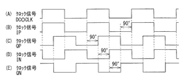
- FIG. 2 shows an operation example of the signal generation circuit 16, (A) shows the waveform of the clock signal DCOCLK, and (B) to (E) show the waveforms of the clock signals IP, QP, IN, and QN.
- the clock signal IP has the same phase as the clock signal DCOCLK.
- the clock signal QP has a phase delayed by 90 degrees (1/4 cycle) from the clock signal IP
- the clock signal IN has a phase delayed by 90 degrees from the clock signal QP
- QN has a phase delayed by 90 degrees with respect to the clock signal IN and has a phase advanced by 90 degrees with respect to the clock signal IP.
- the signal generation circuit 16 sequentially selects one of the four clock signals IP, QP, IN, and QN based on the reference clock signal REFCLK and the phase rotation word PRW to generate the clock signal CLK.
- the signal generation circuit 16 uses four clocks in each of the periods PR corresponding to one cycle of the reference clock signal REFCLK.
- a clock signal whose phase is delayed by a quarter cycle from the selected clock signal among the signals IP, QP, IN, and QN is newly selected. That is, for example, the signal generation circuit 16 newly selects the clock signal QP when the clock signal IP is selected, and newly selects the clock signal IN when the clock signal QP is selected.
- the clock signal IN is selected
- the clock signal QN is newly selected, and when the clock signal QN is selected, the clock signal IP is newly selected to switch the clock signal.
- the signal generation circuit 16 selects one of the four clock signals IP, QP, IN, and QN in each period PR.
- a clock signal whose phase is advanced by 1 ⁇ 4 period from the clock signal is newly selected. That is, for example, the signal generation circuit 16 newly selects the clock signal QN when the clock signal IP is selected, and newly selects the clock signal IP when the clock signal QP is selected.
- the clock signal IN is selected, the clock signal QP is newly selected, and when the clock signal QN is selected, the clock signal IN is newly selected to switch the clock signal.
- the phase rotation value P is “ ⁇ 1/4” as described above, the signal generation circuit 16 switches the clock signal a plurality of times in each period PR, as will be described later. A clock signal whose phase is advanced by a period is newly selected.
- the phase detection circuit 20 detects the phase of the clock signal CLK based on the clock signal CLK and the reference clock signal REFCLK, and outputs the detection result as the phase word PW2.
- the phase detection circuit 20 includes an accumulator 21, a TDC (Time-to-Digital Converter) 22, and an adder circuit 23.
- the accumulator 21 acquires the integer part of the phase value of the clock signal CLK by counting the number of pulses of the clock signal CLK, and outputs it as the phase word D1.
- the TDC 22 obtains the decimal part of the phase value of the clock signal CLK by comparing the transition timing of the clock signal CLK with the transition timing of the reference clock signal REFCLK, and outputs it as the phase word D2.
- FIG. 3 shows an input signal of the TDC 22, wherein (A) shows the waveform of the reference clock signal REFCLK, and (B) shows the waveform of the clock signal CLK.
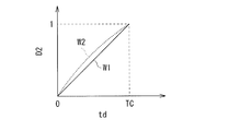
- FIG. 4 shows an example of conversion characteristics in the TDC 22.
- the TDC 22 obtains the position of the rising timing of the reference clock signal REFCLK in the period PC (time TC) corresponding to one cycle of the clock signal CLK.
- the TDC 22 outputs a value corresponding to the time td from the rising timing t1 of the clock signal CLK to the rising timing t2 of the reference clock signal REFCLK as the phase word D2.
- the value of the phase word D2 is 0 or more and less than 1, and increases with time td.
- the conversion characteristic of the TDC 22 is desirably a linear characteristic as indicated by the characteristic W1, but may have non-linearity as indicated by the characteristic W2.
- the phase synchronization circuit 1 since the signal generation circuit 16 is provided, the possibility that the phase noise of the clock signal DCOCLK increases can be reduced even when the TDC 22 has nonlinear conversion characteristics, as will be described later. It has become.
- the addition circuit 23 generates the phase word PW2 based on the phase words D1 and D2. That is, since the phase word D1 indicates the integer part of the phase value of the clock signal CLK and the phase word D2 indicates the fractional part of the phase value of the clock signal CLK, the adder circuit 23 has the value and the phase indicated by the phase word D1. The phase value of the clock signal CLK is obtained by adding the value indicated by the word D2. The adder circuit 23 outputs the addition result as the phase word PW2.
- the clock signal DCOCLK corresponds to a specific example of “first clock” in the present disclosure
- the clock signals IP, QP, IN, and QP are specific examples of “plurality of second clocks” in the present disclosure.
- the clock signal CLK corresponds to a specific example of “third clock” in the present disclosure.
- the reference clock signal REFCLK corresponds to a specific example of “reference clock” in the present disclosure.
- the value of the reference phase word PW1 corresponds to a specific example of “reference phase value” in the present disclosure
- the value of the phase word PW2 corresponds to a specific example of “feedback phase value” in the present disclosure.
- the period PR corresponds to a specific example of “period period” in the present disclosure.
- the control circuit 11 generates a frequency control word FCW and a phase rotation word PRW.
- the reference phase generation circuit 12 generates a reference phase word PW1 based on the frequency control word FCW.
- the phase comparison circuit 13 generates a phase error word PEW based on the reference phase word PW1 and the phase word PW2.
- the loop filter 14 generates a control word CW based on the phase error word PEW.
- the oscillation circuit 15 generates a clock signal DCOCLK based on the control word CW.
- the signal generation circuit 16 generates the clock signal CLK based on the clock signal DCOCLK, the reference clock signal REFCLK, and the phase rotation word PRW. Specifically, the signal generation circuit 16 first generates four clock signals IP, QP, IN, and QN having different phases based on the clock signal DCOCLK. The signal generation circuit 16 generates the clock signal CLK by switching these four clock signals IP, QP, IN, and QN.
- the phase detection circuit 20 detects the phase of the clock signal CLK based on the clock signal CLK and the reference clock signal REFCLK, and outputs the detection result as the phase word PW2. Specifically, the accumulator 21 acquires the integer part of the phase value of the clock signal CLK by counting the number of pulses of the clock signal CLK, and outputs it as the phase word D1. The TDC 22 obtains the decimal part of the phase value of the clock signal CLK by comparing the transition timing of the clock signal CLK with the transition timing of the reference clock signal REFCLK, and outputs it as the phase word D2. The adder circuit 23 generates a phase word PW2 by adding the value indicated by the phase word D1 and the value indicated by the phase word D2.
- phase synchronization circuit 1 Next, the operation of the phase synchronization circuit 1 will be described in detail with some examples.
- a case where the value (frequency ratio fratio) obtained by dividing the frequency fclk of the clock signal DCOCLK by the frequency fref of the reference clock signal REFCLK is “4.1” will be described as an example.
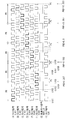
- FIG. 5 shows an example of the operation of the phase synchronization circuit 1.
- (A) to (D) show the waveforms of the four clock signals IP, QP, IN, and QN, respectively, and (E) shows the reference clock signal. The waveform of REFCLK is shown, and (F) shows the waveform of the clock signal CLK.
- the waveform indicated by the thick line indicates the waveform portion selected by the signal generation circuit 16.
- the control circuit 11 sets the value of the frequency control word FCW to “3.85” and the value of the phase rotation word PRW to “+1/4”.
- the signal generation circuit 16 generates four clock signals IP, QP, IN, and QN based on the clock signal DCOCLK, and generates a clock signal CLK by switching these clock signals IP, QP, IN, and QN. Then, the phase detection circuit 20 detects the phase of the clock signal CLK based on the clock signal CLK and the reference clock signal REFCLK. This operation will be described in detail below.
- a period PR corresponding to one cycle of the reference clock REFCLK starts.
- the signal generation circuit 16 switches the clock signal once during the period from timing t11 to t13. Specifically, the signal generation circuit 16 selects the clock signal IP and outputs it as the clock signal CLK in the period from the timing t11 to t12, and switches the clock signal from the clock signal IP to the clock signal QP at the timing t12. (FIG. 5 (A), (B), (F)).
- the phase detection circuit 20 detects the phase of the clock signal and outputs it as the phase word PW2.
- the accumulator 21 outputs the phase word D1 indicating the value “3”.
- the TDC 22 obtains the position of the rising timing (timing t13) of the reference clock signal REFCLK in the period PC corresponding to one cycle of the clock signal CLK.
- the TDC 22 outputs a phase word D2 indicating the value “0.85”.
- the reference phase generation circuit 12 generates the reference phase word PW1 based on the frequency control word FCW.
- the frequency control word FCW is “3.85”
- phase synchronization is maintained in the phase synchronization circuit 1.
- a new period PR starts at this timing t13, and the signal generation circuit 16 switches the clock signal from the clock signal QP to the clock signal IN at the timing t14 (FIGS. 5B, 5C, and 5C). F)).
- the period PR ends.
- the accumulator 21 outputs the phase word D1 indicating the value “7”.
- the TDC 22 outputs the phase word D2 indicating the value “0.7”.
- phase comparison circuit 13 determines the difference between the value “7.7” of the reference phase word PW1 and the value “7.7” of the phase word PW2, thereby generating the phase error word PEW having the value “0”. .
- phase synchronization is maintained in the phase synchronization circuit 1.
- a new period PR starts at this timing t15, and the signal generation circuit 16 switches the clock signal from the clock signal IN to the clock signal QN at the timing t16 (FIGS. 5C, 5D, and 5D). F)).
- phase comparison circuit 13 determines the difference between the value “11.55” of the reference phase word PW1 and the value “11.55” of the phase word PW2, thereby generating the phase error word PEW having the value “0”. .
- phase synchronization is maintained in the phase synchronization circuit 1.
- a new period PR starts at this timing t17, and the signal generation circuit 16 switches the clock signal from the clock signal QN to the clock signal IP at the timing t18 (FIGS. 5A, 5D, (D), F)).
- phase comparison circuit 13 determines the difference between the value “15.4” of the reference phase word PW1 and the value “15.4” of the phase word PW2, thereby generating the phase error word PEW having the value “0”. .
- phase synchronization is maintained in the phase synchronization circuit 1.
- a new period PR starts at this timing t19, and the signal generation circuit 16 switches the clock signal from the clock signal IP to the clock signal QP at the timing t20 (FIGS. 5A, 5B, ( F)).
- phase comparison circuit 13 determines the difference between the value “19.25” of the reference phase word PW1 and the value “19.25” of the phase word PW2, thereby generating the phase error word PEW having the value “0”. .
- phase synchronization is maintained in the phase synchronization circuit 1.
- the signal generation circuit 16 sequentially switches the four clock signals IP, QP, IN, and QN to generate the clock signal CLK, and the phase detection circuit 20 uses the phase of the clock signal CLK. It was made to detect. Thereby, as will be described later in comparison with Comparative Example 1, phase noise can be reduced even when the TDC 22 has a nonlinear conversion characteristic.
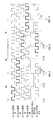
- FIG. 6 shows another operation example of the phase synchronization circuit 1.
- the control circuit 11 sets the value of the frequency control word FCW to “3.35” and the value of the phase rotation word PRW to “ ⁇ 1/4”.
- a period PR corresponding to one cycle of the reference clock REFCLK starts.
- the signal generation circuit 16 switches the clock signal three times during the period from timing t21 to t25. Specifically, the signal generation circuit 16 selects the clock signal IP and outputs it as the clock signal CLK during the period of timing t21 to t22, and switches the clock signal from the clock signal IP to the clock signal QP at timing t22.
- the clock signal is switched from the clock signal QP to the clock signal IN, and at timing t24, the clock signal is switched from the clock signal IN to the clock signal QN (FIGS. 6A to 6D and 6F).
- phase comparison circuit 13 determines the difference between the value “3.35” of the reference phase word PW1 and the value “3.35” of the phase word PW2, thereby generating the phase error word PEW having the value “0”. .
- phase synchronization is maintained in the phase synchronization circuit 1.
- a new period PR starts at this timing t25, and the signal generation circuit 16 sequentially switches the clock signal from the clock signal QN to the clock signals IP, QP and IN at the timings t26, t27 and t28 (FIG. 6 (A) to (D), (F)).
- phase comparison circuit 13 determines the difference between the value “6.7” of the reference phase word PW1 and the value “6.7” of the phase word PW2, thereby generating the phase error word PEW having the value “0”. .
- phase synchronization is maintained in the phase synchronization circuit 1.
- a new period PR starts, and the signal generation circuit 16 sequentially switches the clock signal from the clock signal IN to the clock signals QN, IP, and QP at the timings t30, t31, and t32 (FIG. 6 (A) to (D), (F)).
- phase comparison circuit 13 calculates the difference between the value “10.05” of the reference phase word PW1 and the value “10.05” of the phase word PW2, thereby generating the phase error word PEW having the value “0”. .
- phase synchronization is maintained in the phase synchronization circuit 1.
- a new period PR starts, and the signal generation circuit 16 sequentially switches the clock signal from clock signal QP to clock signals IN, QN, and IP at timings t34, t35, and t36 (FIG. 6 (A) to (D), (F)).
- phase comparison circuit 13 determines the difference between the value “13.4” of the reference phase word PW1 and the value “13.4” of the phase word PW2, thereby generating the phase error word PEW having the value “0”. .
- phase synchronization is maintained in the phase synchronization circuit 1.
- a new period PR starts, and the signal generation circuit 16 sequentially switches the clock signal from the clock signal IP to the clock signals QP, IN, QN at the timings t38, t39, t40 (FIG. 6 (A) to (D), (F)).
- phase comparison circuit 13 determines the difference between the value “16.75” of the reference phase word PW1 and the value “16.75” of the phase word PW2, thereby generating the phase error word PEW having the value “0”. .
- phase synchronization is maintained in the phase synchronization circuit 1.
- phase synchronization circuit 1 when the value of the phase rotation word PRW is “ ⁇ 1/4, the signal generation circuit 16 performs clocks in the order of IP, QP, IN, QN,.
- the signal is switched a plurality of times (in this example, three times), thereby reducing the possibility that the pulse width of the clock signal CLK is narrowed, as will be described below in comparison with Comparative Example 2.
- the possibility that the phase detection circuit 20 malfunctions can be reduced, and phase noise can be reduced.
- the phase synchronization circuit 1R according to the first comparative example is obtained by omitting the signal generation circuit 16 from the phase synchronization circuit 1 according to the present embodiment. That is, in the first comparative example, the phase detection circuit 20 detects the phase of the clock signal CLK based on the clock signal DCOCLK and the reference clock signal REFCLK, and outputs the detection result as the phase word PW2. Other configurations are the same as those of the present embodiment (FIG. 1).
- the frequency control word generation circuit 11 sets the frequency control word FCW to “4.1”.
- phase synchronization is maintained in the phase synchronization circuit 1R.
- the value of the reference phase word PW1 increases like 4.1, 8.2, 12.3, 16.4, 20.5,.
- the value of PW2 increases as 4.1, 8.2, 12.3, 16.4, 20.5,. Therefore, at each of the timings t52 to t56, the value of the phase error word PEW becomes “0”, and as a result, the phase synchronization is maintained in the phase synchronization circuit 1R.
- the TDC 22 has nonlinear conversion characteristics.
- the value of the reference phase word PW1 and the value of the phase word PW2 match at each timing.
- the value of the reference phase word PW1 and the value of the phase word PW2 are transiently shifted.
- FIG. 8 shows the operation of the phase locked loop 1R when the TDC 22 has a nonlinear conversion characteristic.
- (A) shows the value of the phase word D2 output from the TDC 22, and
- (B) shows the phase error word. Indicates the value of PEW.
- the horizontal axis represents time, and one scale corresponds to the time of one cycle of the reference clock REFCLK.
- the value of the phase word D2 repeats the behavior of increasing from “0” to “1”. That is, the value of the phase word D2 increases in order, similar to the change of the decimal part (0.1, 0.2, 0.3, 0.4, 0.5,...) Shown in FIG. To do. At this time, the value of the phase word D2 changes nonlinearly corresponding to the nonlinear conversion characteristic of the TDC 22. On the other hand, the value of the reference phase word PW1 increases linearly. Therefore, the value of the phase error word PEW fluctuates at a predetermined cycle as shown in FIG.
- the frequency fn1 of the fluctuation can be expressed using the following equation.
- n fref ⁇ n (1)
- n is a decimal part of the frequency ratio fratio.
- fref 8 [MHz]
- the frequency ratio fratio 4.1 (that is, n is 0.1)
- the frequency fn1 is 0.8 [MHz].
- the oscillation circuit 15 modulates the clock signal DCOCLK at the frequency fn1.
- the signal generation circuit 16 sequentially switches the four clock signals IP, QP, IN, and QN to generate the clock signal CLK, and the phase detection circuit 20 The phase of the signal CLK is detected.
- FIG. 9 shows the operation of the phase locked loop 1 when the TDC 22 has a nonlinear conversion characteristic.
- (A) shows the value of the phase word D2 output from the TDC 22, and (B) shows the phase error word. Indicates the value of PEW.
- FIG. 9 corresponds to Operation Example 1 (FIG. 5).
- the conversion characteristic labeled “IP” indicates the conversion characteristic when the signal generation circuit 16 selects the clock signal IP.
- conversion characteristics labeled “QP”, “IN”, and “QN” indicate conversion characteristics when the signal generation circuit 16 selects the clock signals QP, IN, and QN, respectively.
- the value of the phase word D2 repeats the behavior of decreasing from “1” to “0”. That is, the value of the phase word D2 sequentially decreases in the same manner as the change of the decimal part (0.85, 0.7, 0.55, 0.4, 0.25,...) Of the phase word PW2 shown in FIG. To do. At this time, the value of the phase word D2 changes nonlinearly corresponding to the nonlinear conversion characteristic of the TDC 22. Therefore, the value of the phase error word PEW fluctuates at a predetermined cycle as shown in FIG.
- the period of fluctuation of the value of the phase error word PEW can be made shorter than in the case of the phase locked loop 1R according to Comparative Example 1 (broken line in FIG. 9B). Therefore, for example, by setting the fluctuation frequency fn2 to a high value so as to be outside the loop band of the phase synchronization circuit 1, the possibility that the clock signal DCOCLK is modulated can be reduced. The possibility that the phase noise will be reduced can be reduced.
- the frequency fn2 can be expressed by the following equation.
- fn2 fref ⁇ F [VPR ⁇ n] (2)
- VPR is the value of the phase rotation word PRW (phase rotation value)
- F extracts only the decimal part of the argument.
- fref 8 [MHz]
- the frequency ratio fratio is 4.1 (that is, n is 0.1)
- the phase rotation value VPR is “+1/4”
- the frequency fn2 is 1. 2 [MHz].
- the clock signal CLK is generated by sequentially switching the four clock signals IP, QP, IN, and QN. Therefore, even when the TDC 22 has nonlinear conversion characteristics, The possibility that the phase noise of the clock signal DCOCLK is deteriorated can be reduced.
- phase synchronization circuit 1S according to the second comparative example performs a different operation from the signal generation circuit 16 according to the present embodiment when the value of the phase rotation word PRW is “ ⁇ 1/4”. It is what has.
- Other configurations are the same as those of the present embodiment (FIG. 1).
- FIG. 10 shows the operation of the phase synchronization circuit 1S.
- the value of the frequency control word FCW is set to “4.35”
- the value of the phase rotation word PRW is set to “ ⁇ 1/4”.
- the period PR starts.
- the signal generation circuit 16S switches the clock signal once during the period from timing t61 to t65. Specifically, the signal generation circuit 16S selects the clock signal IP and outputs it as the clock signal CLK in the period from timing t61 to t62, and switches the clock signal from the clock signal IP to the clock signal QN at timing t62 ( FIG. 10 (A), (D), (F)).
- phase comparison circuit 13 determines the difference between the value “4.35” of the reference phase word PW1 and the value “4.35” of the phase word PW2, thereby generating the phase error word PEW having the value “0”. .
- phase synchronization is maintained in the phase synchronization circuit 1S. The same applies to the operation after timing t63.
- phase synchronization circuit 1S when the clock signal is switched at the timing t62 and the like, a narrow pulse (part W3) appears in the clock signal CLK.
- the phase detection circuit 20 may malfunction and cannot normally detect the phase of the clock signal CLK. In such a case, the value of the phase error word PEW may fluctuate transiently and the phase noise of the clock signal DCOCLK may deteriorate.
- the signal generation circuit 16 when the value of the phase rotation word PRW is “ ⁇ 1/4”, the signal generation circuit 16 performs IP, QP, IN, QN in each period PR. ,... Are switched multiple times in this order (three times in this example). That is, for example, in the period PR from timing t21 to t25 in FIG. 6, the signal generation circuit 16 does not directly switch the clock signal from the clock signal IP to the clock signal QN, but first switches from the clock signal IP to the clock signal QP. Then, the clock signal QP is switched to the clock signal IN, and then the clock signal IN is switched to the clock signal QN.
- phase rotation word PRW when the value of the phase rotation word PRW is “ ⁇ 1/4”, switching is performed a plurality of times in the order of IP, QP, IN, QN,. Since the possibility that the pulse width becomes narrow in CLK can be reduced, the possibility that the phase noise of the clock signal DCOCLK is deteriorated can be reduced.
- the signal generation circuit 16 performs IP, QP, IN, QN,.
- the clock signal is switched three times in order, the present invention is not limited to this.
- the signal generation circuit 16 may switch the clock signal twice in each period PR.
- the signal generation circuit 16 outputs the clock signal IP as the clock signal CLK in the period from the timing t71 to t72, switches the clock signal from the clock signal IP to the clock signal IN at the timing t72, and at the timing t73.
- the clock signal is switched from the clock signal IN to the clock signal QN. Even if it does in this way, the effect similar to the case of the said embodiment can be acquired.
- the switching timing when the signal generation circuit 16 switches the clock signal a plurality of times in each period PR is the example of FIG. It is not limited to.
- the signal generation circuit 16 switches the clock signal from the clock signal IP to the clock signal QP, and then the clock signal CLK is inverted, and at the subsequent timing t83, the signal generation circuit 16 The clock signal is switched from the clock signal QP to the clock signal IN, the clock signal CLK is then inverted, and the signal generation circuit 16 switches the clock signal from the clock signal IN to the clock signal QN at the subsequent timing t84.
- Good Even if it does in this way, the effect similar to the case of the said embodiment can be acquired.
- the signal generation circuit 16 generates the four-phase clock signals IP, QP, IN, and QN.
- the present invention is not limited to this, and a clock signal of three or less phases may be generated. Five or more phase clock signals may be generated.
- a case where the 6-phase clock signals CLK1 to CLK6 are generated will be described as an example.
- FIG. 13 shows an example of the operation of the phase locked loop 1C according to this modification.
- (A) to (F) show the waveforms of the six clock signals CLK1 to CLK6, and (G) shows the reference clock. The waveform of the signal REFCLK is shown, and (H) shows the waveform of the clock signal CLK.
- the control circuit 11 sets the value of the frequency control word FCW to “3.933” and the value of the phase rotation word PRW to “+1/6”.
- the value of the frequency control word FCW and the value of the phase word PW2 are shown in the range up to the third decimal place.
- a period PR corresponding to one cycle of the reference clock REFCLK starts.
- the signal generation circuit 16C of the phase synchronization circuit 1C switches the clock signal once during the period from the timing t91 to t93. Specifically, the signal generation circuit 16C switches the clock signal from the clock signal CLK1 to the clock signal CLK2 at the timing t92.
- phase comparison circuit 13 generates the phase error word PEW having the value “0” by obtaining the difference between the value “3.933” of the reference phase word PW1 and the value “3.933” of the phase word PW2. .
- phase synchronization is maintained in the phase synchronization circuit 1C. The same applies to the operation after timing t93.
- FIG. 14 shows another operation example of the phase synchronization circuit 1C.
- the control circuit 11 sets the value of the frequency control word FCW to “3.267” and the value of the phase rotation word PRW to “ ⁇ 1/6”.
- a period PR corresponding to one cycle of the reference clock REFCLK starts.
- the signal generation circuit 16C switches the clock signal three times during the period from the timing t101 to t105. Specifically, the signal generation circuit 16C sequentially switches the clock signal in order from the clock signal CLK1 to the clock signals CLK3, CLK5, and CLK6 at timings t102, t103, and t104.
- phase synchronization is maintained in the phase synchronization circuit 1C. The same applies to the operation after timing t105.
- the value of the phase rotation word PRW is set to “ ⁇ 1/6”.
- the value is not limited to this.
- an example in which the value of the phase rotation word PRW is set to “+2/6” and an example in which the value is set to “ ⁇ 2/6” will be described.
- FIG. 15 shows another operation example of the phase locked loop 1C according to this modification.
- the control circuit 11 sets the value of the frequency control word FCW to “3.767” and the value of the phase rotation word PRW to “+2/6”.
- a period PR corresponding to one cycle of the reference clock REFCLK starts.
- the signal generation circuit 16C of the phase synchronization circuit 1C switches the clock signal once during the period from the timing t111 to t113. Specifically, the signal generation circuit 16C switches the clock signal from the clock signal CLK1 to the clock signal CLK3 at the timing t112.
- phase comparison circuit 13 generates the phase error word PEW having the value “0” by obtaining the difference between the value “3.767” of the reference phase word PW1 and the value “3.767” of the phase word PW2. .
- phase synchronization is maintained in the phase synchronization circuit 1C. The same applies to the operation after timing t113.
- FIG. 16 illustrates another operation example of the phase synchronization circuit 1C.
- the control circuit 11 sets the value of the frequency control word FCW to “3.433” and the value of the phase rotation word PRW to “ ⁇ 2/6”.
- a period PR corresponding to one cycle of the reference clock REFCLK starts.
- the signal generation circuit 16C switches the clock signal twice during the period from the timing t121 to t124. Specifically, the signal generation circuit 16C sequentially switches the clock signal from the clock signal CLK1 to the clock signals CLK3 and CLK5 at timings t122 and t123.
- phase comparison circuit 13 determines the difference between the value “3.433” of the reference phase word PW1 and the value “3.433” of the phase word PW2, thereby generating the phase error word PEW having the value “0”. .
- phase synchronization is maintained in the phase synchronization circuit 1C. The same applies to the operation after timing t124.
- the signal generation circuit 16C generates the six-phase clock signals CLK1 to CLK6, thereby increasing the degree of freedom in setting the phase rotation word PRW.
- the frequency fn2 of the fluctuation of the phase error word PEW can be set more freely using the equation (2), and the clock signal DCOCLK The phase noise can be adjusted more freely so that it can be reduced.
- the value (frequency ratio fratio) obtained by dividing the frequency fclk of the clock signal DCOCLK by the frequency fref of the reference clock signal REFCLK is set to “4.1”, but the present invention is not limited to this.
- the frequency ratio fratio is set to “4.25”
- FIG. 17 shows an operation example of the phase locked loop 1D according to the present modification.
- the control circuit 11 sets the value of the frequency control word FCW to “4” and the value of the phase rotation word PRW to “+1/4”.
- a period PR corresponding to one cycle of the reference clock REFCLK starts.
- the signal generation circuit 16 switches the clock signal once during the period from the timing t131 to t133. Specifically, the signal generation circuit 16 switches the clock signal from the clock signal IP to the clock signal QP at the timing t132.
- phase comparison circuit 13 determines the difference between the value “4” of the reference phase word PW1 and the value “4” of the phase word PW2, thereby generating the phase error word PEW having the value “0”. As a result, phase synchronization is maintained in the phase synchronization circuit 1D. The same applies to the operation after timing t133.
- FIG. 18 illustrates another operation example of the phase synchronization circuit 1D.
- the control circuit 11 sets the value of the frequency control word FCW to “3.5” and the value of the phase rotation word PRW to “ ⁇ 1/4”.
- a period PR corresponding to one cycle of the reference clock REFCLK starts.
- the signal generation circuit 16 switches the clock signal three times during the period from the timing t141 to t145. Specifically, the signal generation circuit 16 sequentially switches the clock signal from the clock signal IP to the clock signals QP, IN, and QN at timings t142, t143, and t144.
- phase comparison circuit 13 calculates the difference between the value “3.5” of the reference phase word PW1 and the value “3.5” of the phase word PW2, thereby generating the phase error word PEW having the value “0”. .
- phase synchronization is maintained in the phase comparison circuit 1D. The same applies to the operation after timing t145.
- the values of various parameters such as the frequency control word FCW, the phase rotation word PRW, and the frequency ratio fratio are exemplified, but the present invention is not limited to this, and can be set as appropriate. .
- the present technology may be applied to a frequency synthesizer used in a wireless communication system, for example.
- the frequency control word FCW and the phase rotation word PRW may be switched according to the frequency (channel) of the clock signal DCOCLK.
- the present technology can be applied to various uses including the phase synchronization circuit.
- phase synchronization circuit according to (1) or (2), wherein, when the plurality of second clocks are switched, the signal generation circuit switches to a clock having a phase delayed from the currently selected clock.
- (4) further comprising a control circuit for generating the first set value and the second set value;
- the reference phase generation circuit sequentially generates the reference phase value based on the first set value;
- the phase according to any one of (1) to (3), wherein the signal generation circuit switches the plurality of second clocks a plurality of times in an order pattern according to the second set value in each cycle period. Synchronous circuit.
- phase synchronization circuit according to (4), wherein the control circuit is configured to be capable of generating a plurality of set value sets including the first set value and the second set value.
- the phase detection circuit includes: A first detection circuit for determining an integer part of the phase value; A phase synchronization circuit according to any one of (1) to (5), further comprising: a second detection circuit that obtains a decimal part of the phase value.
- the second detection circuit obtains a fractional part of the phase value based on a time difference between the transition timing of the reference clock and the transition timing of the third clock.
- (9) having a first operation mode and a second operation mode; In the first operation mode, the signal generation circuit switches the plurality of second clocks a plurality of times in each cycle period, In the second operation mode, the signal generation circuit switches the plurality of second clocks once in each cycle period.
- the phase synchronization circuit according to any one of (1) to (8).
- (10) a reference phase generation circuit that sequentially generates reference phase values;
- An oscillation circuit that generates a first clock based on a difference between the reference phase value and the feedback phase value;
- a signal generation circuit for generating a third clock A frequency synthesizer comprising: a phase detection circuit that obtains a phase value of the third clock and outputs the phase value as the feedback phase value.
Landscapes
- Stabilization Of Oscillater, Synchronisation, Frequency Synthesizers (AREA)
Abstract
本開示の位相同期回路は、基準位相値を順次生成する基準位相生成回路と、基準位相値と帰還位相値との差に基づいて第1のクロックを生成する発振回路と、第1のクロックに基づいて、互いに異なる位相を有する複数の第2のクロックを生成し、基準クロックの1周期に対応する周期期間のそれぞれにおいて複数の第2のクロックを複数回切り替えることにより第3のクロックを生成する信号生成回路と、第3のクロックの位相値を求めて帰還位相値として出力する位相検出回路とを備える。
Description
本開示は、デジタル信号を用いて動作する位相同期回路、および周波数シンセサイザに関する。
近年、様々な電子機器に無線通信機能が搭載される。無線通信システムでは、所望の周波数の信号を生成するために、周波数シンセサイザ(位相同期回路)が搭載される。このような周波数シンセサイザは、アナログPLLや、デジタルPLL(ADPLL;All-digital Phase Locked Loop)(例えば特許文献1~3)を含んで構成される。周波数シンセサイザをデジタルPLLにより構成した場合には、アナログPLLにより構成した場合に比べて、例えば、集積回路のレイアウト面積を小さくし、消費電力を低減することができる。
このようなデジタルPLLでは、生成する信号の位相雑音を低減するための様々な技術が開示されている。例えば、非特許文献1には、発振回路から出力される信号に基づいて4相信号を生成し、その4相信号のうちの1つをフィードバックさせる回路が開示されている。
Staszewski, R.B.; Vemulapalli, S.; Waheed, K., "An all-digital offset PLL architecture," Radio Frequency Integrated Circuits Symposium (RFIC), 2010 IEEE, p.17-20
このように、周波数シンセサイザでは、位相雑音が低いことが望まれており、さらなる位相雑音の低減が期待されている。
したがって、位相雑音を低減することができる位相同期回路および周波数シンセサイザを提供することが望ましい。
本開示の一実施の形態における位相同期回路は、基準位相生成回路と、発振回路と、信号生成回路と、位相検出回路とを備えている。基準位相生成回路は、基準位相値を順次生成する。発振回路は、基準位相値と帰還位相値との差に基づいて第1のクロックを生成するものである。信号生成回路は、第1のクロックに基づいて、互いに異なる位相を有する複数の第2のクロックを生成し、基準クロックの1周期に対応する周期期間のそれぞれにおいて複数の第2のクロックを複数回切り替えることにより第3のクロックを生成するものである。位相検出回路は、第3のクロックの位相値を求めて帰還位相値として出力するものである。
本開示の一実施の形態における周波数シンセサイザは、基準位相生成回路と、発振回路と、信号生成回路と、位相検出回路とを備えている。基準位相生成回路は、基準位相値を順次生成する。発振回路は、基準位相値と帰還位相値との差に基づいて第1のクロックを生成するものである。信号生成回路は、第1のクロックに基づいて、互いに異なる位相を有する複数の第2のクロックを生成し、基準クロックの1周期に対応する周期期間のそれぞれにおいて複数の第2のクロックを複数回切り替えることにより第3のクロックを生成するものである。位相検出回路は、第3のクロックの位相値を求めて帰還位相値として出力するものである。
本開示の一実施の形態における位相同期回路および周波数シンセサイザでは、基準位相値が順次生成され、基準位相値と帰還位相値(第3のクロックの位相値)との差に基づいて、第1のクロックが生成され、第1のクロックに基づいて第3のクロックが生成される。その際、第1のクロックに基づいて、互いに異なる位相を有する複数の第2のクロックが生成され、各周期期間において複数の第2のクロックを複数回切り替えることにより第3のクロックが生成される。
本開示の一実施の形態における位相同期回路および周波数シンセサイザによれば、第1のクロックに基づいて複数の第2のクロックを生成し、各周期期間において複数の第2のクロックを複数回切り替えることにより第3のクロックを生成したので、位相雑音を低減することができる。なお、ここに記載された効果は必ずしも限定されるものではなく、本開示中に記載されたいずれの効果があってもよい。
以下、本開示の実施の形態について、図面を参照して詳細に説明する。
[構成例]
図1は、一実施の形態に係る位相同期回路(位相同期回路1)の一構成例を表すものである。図1では、太線で示した配線は、複数のビットからなるワードを伝えるいわゆるバス配線を示し、細線で示した配線は、1つの信号または差動信号を伝える配線を示す。
図1は、一実施の形態に係る位相同期回路(位相同期回路1)の一構成例を表すものである。図1では、太線で示した配線は、複数のビットからなるワードを伝えるいわゆるバス配線を示し、細線で示した配線は、1つの信号または差動信号を伝える配線を示す。
位相同期回路1は、デジタル回路で構成されたデジタルPLLであり、基準クロック信号REFCLKに基づいて、クロック信号DCOCLKを生成するものである。このクロック信号DCOCLKの周波数fclkは、基準クロック信号REFCLKの周波数frefよりも高いものである。位相同期回路1は、制御回路11と、基準位相生成回路12と、位相比較回路13と、ループフィルタ14と、発振回路15と、信号生成回路16と、位相検出回路20とを備えている。
制御回路11は、周波数制御ワードFCWを生成して基準位相生成回路12に供給するとともに、位相ローテーションワードPRWを生成して信号生成回路16に供給するものである。制御回路11は、この周波数制御ワードFCWおよび位相ローテーションワードPRWにより、発振回路15が生成するクロック信号DCOCLKの周波数fclkを制御するようになっている。
基準位相生成回路12は、周波数制御ワードFCWに基づいて、基準位相ワードPW1を生成するものである。具体的には、基準位相生成回路12は、周波数制御ワードFCWが示す値を累積加算して、基準位相値を生成し、その基準位相値を基準位相ワードPW1として出力するようになっている。
位相比較回路13は、基準位相ワードPW1および位相ワードPW2に基づいて、位相誤差ワードPEWを生成するものである。具体的には、位相比較回路13は、基準位相ワードPW1が示す基準位相値から、位相ワードPW2が示す位相値を減算することにより、位相誤差値を求め、その位相誤差値を位相誤差ワードPEWとして出力するようになっている。
ループフィルタ14は、位相誤差ワードPEWに基づいて、制御ワードCWを生成するものである。具体的には、ループフィルタ14は、位相誤差ワードPEWが示す位相誤差値を平滑化し、その平滑化された位相誤差値を制御ワードCWとして出力するようになっている。
発振回路15は、制御ワードCWに基づいて、クロック信号DCOCLKを生成するものである。そして、発振回路15は、生成したクロック信号DCOCLKを、信号生成回路16に供給するとともに、位相同期回路1の出力端子TOUTから出力するようになっている。
信号生成回路16は、クロック信号DCOCLK、基準クロック信号REFCLK、および位相ローテーションワードPRWに基づいて、クロック信号CLKを生成するものである。具体的には、信号生成回路16は、まず、クロック信号DCOCLKに基づいて、互いに位相が異なる4つのクロック信号IP,QP,IN,QNを生成する。そして、信号生成回路16は、これらの4つのクロック信号IP,QP,IN,QNを切り替えることによりクロック信号CLKを生成するようになっている。
図2は、信号生成回路16の一動作例を表すものであり、(A)はクロック信号DCOCLKの波形を示し、(B)~(E)はクロック信号IP,QP,IN,QNの波形をそれぞれ示す。この例では、クロック信号IPは、クロック信号DCOCLKと同じ位相を有するものである。そして、クロック信号QPは、クロック信号IPよりも位相が90度(1/4周期)遅れたものであり、クロック信号INは、クロック信号QPよりも位相が90度遅れたものであり、クロック信号QNは、クロック信号INよりも位相が90度遅れたものであり、クロック信号IPよりも位相が90度進んだものである。
信号生成回路16は、基準クロック信号REFCLK、および位相ローテーションワードPRWに基づいて、4つのクロック信号IP,QP,IN,QNのうちの1つを順次選択してクロック信号CLKを生成する。
具体的には、例えば、位相ローテーションワードPRWの値が“+1/4”である場合には、信号生成回路16は、基準クロック信号REFCLKの1周期に対応する期間PRのそれぞれにおいて、4つのクロック信号IP,QP,IN,QNのうちの選択されているクロック信号よりも1/4周期だけ位相が遅れたクロック信号を新たに選択する。すなわち、例えば、信号生成回路16は、クロック信号IPが選択されている場合にはクロック信号QPを新たに選択し、クロック信号QPが選択されている場合にはクロック信号INを新たに選択し、クロック信号INが選択されている場合にはクロック信号QNを新たに選択し、クロック信号QNが選択されている場合にはクロック信号IPを新たに選択することにより、クロック信号の切り替えを行う。
また、例えば、位相ローテーション値Pが“-1/4”である場合には、信号生成回路16は、各期間PRにおいて、4つのクロック信号IP,QP,IN,QNのうちの選択されているクロック信号よりも1/4周期だけ位相が進んだクロック信号を新たに選択する。すなわち、例えば、信号生成回路16は、クロック信号IPが選択されている場合にはクロック信号QNを新たに選択し、クロック信号QPが選択されている場合にはクロック信号IPを新たに選択し、クロック信号INが選択されている場合にはクロック信号QPを新たに選択し、クロック信号QNが選択されている場合にはクロック信号INを新たに選択することにより、クロック信号の切り替えを行う。また、信号生成回路16は、このように位相ローテーション値Pが“-1/4”である場合には、後述するように、各期間PRにおいて、クロック信号を複数回切り替えることにより、1/4周期だけ位相が進んだクロック信号を新たに選択するようになっている。
位相検出回路20は、クロック信号CLKおよび基準クロック信号REFCLKに基づいて、クロック信号CLKの位相を検出し、その検出結果を位相ワードPW2として出力するものである。位相検出回路20は、アキュムレータ21と、TDC(Time to Digital Converter)22と、加算回路23とを有している。
アキュムレータ21は、クロック信号CLKのパルス数を数えることにより、クロック信号CLKの位相値の整数部分を取得し、位相ワードD1として出力するものである。
TDC22は、クロック信号CLKの遷移タイミングと、基準クロック信号REFCLKの遷移タイミングとを比較することにより、クロック信号CLKの位相値の小数部分を取得し、位相ワードD2として出力するものである。
図3は、TDC22の入力信号を表すものであり、(A)は基準クロック信号REFCLKの波形を示し、(B)はクロック信号CLKの波形を示す。図4は、TDC22における変換特性例を表すものである。TDC22は、クロック信号CLKの1周期に対応する期間PC(時間TC)における、基準クロック信号REFCLKの立ち上がりタイミングの位置を求める。具体的には、TDC22は、クロック信号CLKの立ち上がりタイミングt1から、基準クロック信号REFCLKの立ち上がりタイミングt2までの時間tdに応じた値を、位相ワードD2として出力する。位相ワードD2の値は、図4に示したように、0以上1未満であり、時間tdに応じて増加するものである。TDC22の変換特性は、特性W1で示したように、線形な特性であることが望ましいが、特性W2で示したように、非線形性を有してしまう場合がある。位相同期回路1では、信号生成回路16を設けるようにしたので、後述するように、TDC22が非線形な変換特性を有する場合でも、クロック信号DCOCLKの位相雑音が増加するおそれを低減することができるようになっている。
加算回路23は、位相ワードD1,D2に基づいて、位相ワードPW2を生成するものである。すなわち、位相ワードD1は、クロック信号CLKの位相値の整数部分を示し、位相ワードD2は、クロック信号CLKの位相値の小数部分を示すため、加算回路23は、位相ワードD1が示す値と位相ワードD2が示す値とを加算することにより、クロック信号CLKの位相値を求める。そして、加算回路23は、その加算結果を位相ワードPW2として出力するようになっている。
ここで、クロック信号DCOCLKは、本開示における「第1のクロック」の一具体例に対応し、クロック信号IP,QP,IN,QPは、本開示における「複数の第2のクロック」の一具体例に対応し、クロック信号CLKは、本開示における「第3のクロック」の一具体例に対応する。基準クロック信号REFCLKは、本開示における「基準クロック」の一具体例に対応する。基準位相ワードPW1の値は、本開示における「基準位相値」の一具体例に対応し、位相ワードPW2の値は、本開示における「帰還位相値」の一具体例に対応する。期間PRは、本開示における「周期期間」の一具体例に対応する。
[動作および作用]
続いて、本実施の形態の位相同期回路1の動作および作用について説明する。
続いて、本実施の形態の位相同期回路1の動作および作用について説明する。
(全体動作概要)
まず、図1を参照して、位相同期回路1の全体動作概要を説明する。制御回路11は、周波数制御ワードFCWおよび位相ローテーションワードPRWを生成する。基準位相生成回路12は、周波数制御ワードFCWに基づいて、基準位相ワードPW1を生成する。位相比較回路13は、基準位相ワードPW1および位相ワードPW2に基づいて、位相誤差ワードPEWを生成する。ループフィルタ14は、位相誤差ワードPEWに基づいて、制御ワードCWを生成する。発振回路15は、制御ワードCWに基づいて、クロック信号DCOCLKを生成する。
まず、図1を参照して、位相同期回路1の全体動作概要を説明する。制御回路11は、周波数制御ワードFCWおよび位相ローテーションワードPRWを生成する。基準位相生成回路12は、周波数制御ワードFCWに基づいて、基準位相ワードPW1を生成する。位相比較回路13は、基準位相ワードPW1および位相ワードPW2に基づいて、位相誤差ワードPEWを生成する。ループフィルタ14は、位相誤差ワードPEWに基づいて、制御ワードCWを生成する。発振回路15は、制御ワードCWに基づいて、クロック信号DCOCLKを生成する。
信号生成回路16は、クロック信号DCOCLK、基準クロック信号REFCLK、および位相ローテーションワードPRWに基づいて、クロック信号CLKを生成する。具体的には、信号生成回路16は、まず、クロック信号DCOCLKに基づいて、互いに位相が異なる4つのクロック信号IP,QP,IN,QNを生成する。そして、信号生成回路16は、これらの4つのクロック信号IP,QP,IN,QNを切り替えることによりクロック信号CLKを生成する。
位相検出回路20は、クロック信号CLKおよび基準クロック信号REFCLKに基づいて、クロック信号CLKの位相を検出し、その検出結果を位相ワードPW2として出力する。具体的には、アキュムレータ21は、クロック信号CLKのパルス数を数えることにより、クロック信号CLKの位相値の整数部分を取得し、位相ワードD1として出力する。TDC22は、クロック信号CLKの遷移タイミングと、基準クロック信号REFCLKの遷移タイミングとを比較することにより、クロック信号CLKの位相値の小数部分を取得し、位相ワードD2として出力する。加算回路23は、位相ワードD1が示す値と位相ワードD2が示す値とを加算することにより、位相ワードPW2を生成する。
(詳細動作)
次に、位相同期回路1の動作について、いくつかの例をあげて詳細に説明する。ここでは、クロック信号DCOCLKの周波数fclkを基準クロック信号REFCLKの周波数frefで割った値(周波数比fratio)が“4.1”である場合を例に説明する。
次に、位相同期回路1の動作について、いくつかの例をあげて詳細に説明する。ここでは、クロック信号DCOCLKの周波数fclkを基準クロック信号REFCLKの周波数frefで割った値(周波数比fratio)が“4.1”である場合を例に説明する。
(動作例1)
図5は、位相同期回路1の一動作例を表すものであり、(A)~(D)は4つのクロック信号IP,QP,IN,QNの波形をそれぞれ示し、(E)は基準クロック信号REFCLKの波形を示し、(F)はクロック信号CLKの波形を示す。この図5(A)~(D)において、太線で示した波形は、信号生成回路16が選択した波形部分を示している。この例では、制御回路11は、周波数制御ワードFCWの値を“3.85”に設定するとともに、位相ローテーションワードPRWの値を“+1/4”に設定している。
図5は、位相同期回路1の一動作例を表すものであり、(A)~(D)は4つのクロック信号IP,QP,IN,QNの波形をそれぞれ示し、(E)は基準クロック信号REFCLKの波形を示し、(F)はクロック信号CLKの波形を示す。この図5(A)~(D)において、太線で示した波形は、信号生成回路16が選択した波形部分を示している。この例では、制御回路11は、周波数制御ワードFCWの値を“3.85”に設定するとともに、位相ローテーションワードPRWの値を“+1/4”に設定している。
信号生成回路16は、クロック信号DCOCLKに基づいて、4つのクロック信号IP,QP,IN,QNを生成し、これらのクロック信号IP,QP,IN,QNを切り替えてクロック信号CLKを生成する。そして、位相検出回路20が、クロック信号CLKおよび基準クロック信号REFCLKに基づいて、クロック信号CLKの位相を検出する。以下に、この動作について詳細に説明する。
まず、タイミングt11において、基準クロックREFCLKの1周期に対応する期間PRが開始する。信号生成回路16は、タイミングt11~t13の期間において、クロック信号を1回切り替える。具体的には、信号生成回路16は、タイミングt11~t12の期間において、クロック信号IPを選択してクロック信号CLKとして出力し、タイミングt12において、クロック信号を、クロック信号IPからクロック信号QPに切り替える(図5(A),(B),(F))。
そして、タイミングt13において、期間PRが終了し、位相検出回路20は、クロック信号の位相を検出し、位相ワードPW2として出力する。このとき、タイミングt11~t13の期間におけるクロック信号CLKのパルス数は“3”であるため、アキュムレータ21は、値“3”を示す位相ワードD1を出力する。また、TDC22は、クロック信号CLKの1周期に対応する期間PCにおける、基準クロック信号REFCLKの立ち上がりタイミング(タイミングt13)の位置を求める。この例では、TDC22は、値“0.85”を示す位相ワードD2を出力する。その結果、位相検出回路20は、値“3.85”(=3+0.85)を示す位相ワードPW2を生成する。
基準位相生成回路12は、周波数制御ワードFCWに基づいて、基準位相ワードPW1を生成する。この例では、周波数制御ワードFCWは“3.85”であるため、タイミングt13では、基準位相ワードPW1が示す値は“3.85”(=3.85×1)である。よって、位相比較回路13は、基準位相ワードPW1の値“3.85”と位相ワードPW2の値“3.85”との差を求めることにより、値“0”の位相誤差ワードPEWを生成する。その結果、位相同期回路1では位相同期が維持される。
また、このタイミングt13において、新たな期間PRが開始し、信号生成回路16は、タイミングt14において、クロック信号を、クロック信号QPからクロック信号INに切り替える(図5(B),(C),(F))。
そして、タイミングt15において、期間PRが終了する。このとき、タイミングt11~t15の期間におけるクロック信号CLKのパルス数は“7”であるため、アキュムレータ21は、値“7”を示す位相ワードD1を出力する。また、この例では、TDC22は、値“0.7”を示す位相ワードD2を出力する。その結果、位相検出回路20は、値“7.7”(=7+0.7)を示す位相ワードPW2を生成する。このタイミングt15では、基準位相ワードPW1が示す値は“7.7”(=3.85×2)である。よって、位相比較回路13は、基準位相ワードPW1の値“7.7”と位相ワードPW2の値“7.7”との差を求めることにより、値“0”の位相誤差ワードPEWを生成する。その結果、位相同期回路1では位相同期が維持される。
また、このタイミングt15において、新たな期間PRが開始し、信号生成回路16は、タイミングt16において、クロック信号を、クロック信号INからクロック信号QNに切り替える(図5(C),(D),(F))。
そして、タイミングt17において、期間PRが終了し、位相検出回路20は、値“11.55”(=11+0.55)を示す位相ワードPW2を生成する。このタイミングt17では、基準位相ワードPW1が示す値は“11.55”(=3.85×3)である。よって、位相比較回路13は、基準位相ワードPW1の値“11.55”と位相ワードPW2の値“11.55”との差を求めることにより、値“0”の位相誤差ワードPEWを生成する。その結果、位相同期回路1では位相同期が維持される。
また、このタイミングt17において、新たな期間PRが開始し、信号生成回路16は、タイミングt18において、クロック信号を、クロック信号QNからクロック信号IPに切り替える(図5(A),(D),(F))。
そして、タイミングt19において、期間PRが終了し、位相検出回路20は、値“15.4”(=15+0.4)を示す位相ワードPW2を生成する。このタイミングt19では、基準位相ワードPW1が示す値は“15.4”(=3.85×4)である。よって、位相比較回路13は、基準位相ワードPW1の値“15.4”と位相ワードPW2の値“15.4”との差を求めることにより、値“0”の位相誤差ワードPEWを生成する。その結果、位相同期回路1では位相同期が維持される。
また、このタイミングt19において、新たな期間PRが開始し、信号生成回路16は、タイミングt20において、クロック信号を、クロック信号IPからクロック信号QPに切り替える(図5(A),(B),(F))。
そして、タイミングt21において、期間PRが終了し、位相検出回路20は、値“19.25”(=19+0.25)を示す位相ワードPW2を生成する。このタイミングt21では、基準位相ワードPW1が示す値は“19.25”(=3.85×5)である。よって、位相比較回路13は、基準位相ワードPW1の値“19.25”と位相ワードPW2の値“19.25”との差を求めることにより、値“0”の位相誤差ワードPEWを生成する。その結果、位相同期回路1では位相同期が維持される。
このように、位相同期回路1では、信号生成回路16が、4つのクロック信号IP,QP,IN,QNを順次切り替えてクロック信号CLKを生成し、位相検出回路20が、このクロック信号CLKの位相を検出するようにした。これにより、後ほど比較例1と対比して説明するように、TDC22が非線形な変換特性を有する場合であっても、位相雑音を低減することができる。
(動作例2)
図6は、位相同期回路1の他の動作例を表すものである。この例では、制御回路11は、周波数制御ワードFCWの値を“3.35”に設定するとともに、位相ローテーションワードPRWの値を“-1/4”に設定している。
図6は、位相同期回路1の他の動作例を表すものである。この例では、制御回路11は、周波数制御ワードFCWの値を“3.35”に設定するとともに、位相ローテーションワードPRWの値を“-1/4”に設定している。
まず、タイミングt21において、基準クロックREFCLKの1周期に対応する期間PRが開始する。信号生成回路16は、タイミングt21~t25の期間において、クロック信号を3回切り替える。具体的には、信号生成回路16は、タイミングt21~t22の期間において、クロック信号IPを選択してクロック信号CLKとして出力し、タイミングt22において、クロック信号をクロック信号IPからクロック信号QPに切り替え、タイミングt23において、クロック信号をクロック信号QPからクロック信号INに切り替え、タイミングt24において、クロック信号をクロック信号INからクロック信号QNに切り替える(図6(A)~(D),(F))。
そして、タイミングt25において、期間PRが終了し、位相検出回路20は、値“3.35”(=3+0.35)を示す位相ワードPW2を生成する。このタイミングt25では、基準位相ワードPW1が示す値は“3.35”(=3.35×1)である。よって、位相比較回路13は、基準位相ワードPW1の値“3.35”と位相ワードPW2の値“3.35”との差を求めることにより、値“0”の位相誤差ワードPEWを生成する。その結果、位相同期回路1では位相同期が維持される。
また、このタイミングt25において、新たな期間PRが開始し、信号生成回路16は、タイミングt26,t27,t28において、クロック信号を、クロック信号QNからクロック信号IP,QP,INの順に順次切り替える(図6(A)~(D),(F))。
そして、タイミングt29において、期間PRが終了し、位相検出回路20は、値“6.7”(=6+0.7)を示す位相ワードPW2を生成する。このタイミングt29では、基準位相ワードPW1が示す値は“6.7”(=3.35×2)である。よって、位相比較回路13は、基準位相ワードPW1の値“6.7”と位相ワードPW2の値“6.7”との差を求めることにより、値“0”の位相誤差ワードPEWを生成する。その結果、位相同期回路1では位相同期が維持される。
また、このタイミングt29において、新たな期間PRが開始し、信号生成回路16は、タイミングt30,t31,t32において、クロック信号を、クロック信号INからクロック信号QN,IP,QPの順に順次切り替える(図6(A)~(D),(F))。
そして、タイミングt33において、期間PRが終了し、位相検出回路20は、値“10.05”(=10+0.05)を示す位相ワードPW2を生成する。このタイミングt33では、基準位相ワードPW1が示す値は“10.05”(=3.35×3)である。よって、位相比較回路13は、基準位相ワードPW1の値“10.05”と位相ワードPW2の値“10.05”との差を求めることにより、値“0”の位相誤差ワードPEWを生成する。その結果、位相同期回路1では位相同期が維持される。
また、このタイミングt33において、新たな期間PRが開始し、信号生成回路16は、タイミングt34,t35,t36において、クロック信号を、クロック信号QPからクロック信号IN,QN,IPの順に順次切り替える(図6(A)~(D),(F))。
そして、タイミングt37において、期間PRが終了し、位相検出回路20は、値“13.4”(=13+0.4)を示す位相ワードPW2を生成する。このタイミングt37では、基準位相ワードPW1が示す値は“13.4”(=3.35×4)である。よって、位相比較回路13は、基準位相ワードPW1の値“13.4”と位相ワードPW2の値“13.4”との差を求めることにより、値“0”の位相誤差ワードPEWを生成する。その結果、位相同期回路1では位相同期が維持される。
また、このタイミングt37において、新たな期間PRが開始し、信号生成回路16は、タイミングt38,t39,t40において、クロック信号を、クロック信号IPからクロック信号QP,IN,QNの順に順次切り替える(図6(A)~(D),(F))。
そして、タイミングt41において、期間PRが終了し、位相検出回路20は、値“16.75”(=6+0.75)を示す位相ワードPW2を生成する。このタイミングt41では、基準位相ワードPW1が示す値は“16.75”(=3.35×5)である。よって、位相比較回路13は、基準位相ワードPW1の値“16.75”と位相ワードPW2の値“16.75”との差を求めることにより、値“0”の位相誤差ワードPEWを生成する。その結果、位相同期回路1では位相同期が維持される。
このように、位相同期回路1では、位相ローテーションワードPRWの値が“-1/4である場合に、信号生成回路16は、各期間PRにおいて、IP,QP,IN,QN,…の順にクロック信号を複数回(この例では3回)切り替えるようにした。これにより、以下に比較例2と対比して説明するように、クロック信号CLKにおいてパルス幅が狭まるおそれを低減することができるため、位相検出回路20が誤動作を行うおそれを低減することができ、位相雑音を低減することができる。
次に、いくつかの比較例と対比して、本実施の形態の作用を説明する。
(比較例1)
本比較例1に係る位相同期回路1Rは、本実施の形態に係る位相同期回路1から、信号生成回路16を省いたものである。すなわち、本比較例1では、位相検出回路20は、クロック信号DCOCLKおよび基準クロック信号REFCLKに基づいて、クロック信号CLKの位相を検出し、その検出結果を位相ワードPW2として出力する。その他の構成は、本実施の形態(図1)と同様である。
本比較例1に係る位相同期回路1Rは、本実施の形態に係る位相同期回路1から、信号生成回路16を省いたものである。すなわち、本比較例1では、位相検出回路20は、クロック信号DCOCLKおよび基準クロック信号REFCLKに基づいて、クロック信号CLKの位相を検出し、その検出結果を位相ワードPW2として出力する。その他の構成は、本実施の形態(図1)と同様である。
図7は、位相同期回路1Rの動作を表すものであり、(A)は基準クロック信号REFCLKの波形を示し、(B)はクロック信号DCOCLKの波形を示す。この例では、周波数制御ワード生成回路11は、周波数制御ワードFCWを“4.1”に設定している。
まず、タイミングt51において、基準クロックREFCLKの1周期に対応する期間PRが開始し、タイミングt52において、この期間PRが終了する。位相検出回路20は、値“4.1”(=4+0.1)を示す位相ワードPW2を生成する。このタイミングt52では、基準位相ワードPW1が示す値は“4.1”(=4.1×1)である。よって、位相比較回路13は、基準位相ワードPW1の値“4.1”と位相ワードPW2の値“4.1”との差を求めることにより、値“0”の位相誤差ワードPEWを生成する。その結果、位相同期回路1Rでは位相同期が維持される。
タイミングt52以降の動作についても同様であり、基準位相ワードPW1の値は、4.1,8.2,12.3,16.4,20.5,…のように増加していき、位相ワードPW2の値もまた同様に、4.1,8.2,12.3,16.4,20.5,…のように増加していく。よって、タイミングt52~t56のそれぞれにおいて、位相誤差ワードPEWの値は“0”になり、その結果、位相同期回路1Rでは位相同期が維持される。
次に、TDC22が非線形な変換特性を有する場合について説明する。図7の例では、TDC22が線形な変換特性を有するため、各タイミングにおいて、基準位相ワードPW1の値と位相ワードPW2の値とは一致する。しかしながら、例えば図4に示したように、TDC22が非線形な変換特性を有する場合には、基準位相ワードPW1の値と位相ワードPW2の値とが過渡的にずれてしまうおそれがある。
図8は、TDC22が非線形な変換特性を有する場合における位相同期回路1Rの動作を表すものであり、(A)はTDC22から出力される位相ワードD2の値を示し、(B)は位相誤差ワードPEWの値を示す。図8において、横軸は時間であり、1目盛りは、基準クロックREFCLKの1周期分の時間に対応している。
図8(A)に示したように、位相ワードD2の値は、“0”から“1”に向かって増加する振る舞いを繰り返す。すなわち、図7に示した位相ワードPW2の小数部分の変化(0.1,0.2,0.3,0.4,0.5,…)と同様に、位相ワードD2の値は順に増加する。その際、この位相ワードD2の値は、TDC22の非線形な変換特性に対応して、非線形に変化する。一方、基準位相ワードPW1の値は線形に増加する。よって、位相誤差ワードPEWの値は、図8(B)に示したように、所定の周期で揺れてしまう。この揺れの周波数fn1は、次式を用いて表すことができる。
fn1 = fref × n ・・・(1)
ここで、nは、周波数比fratioの小数部分である。例えば、frefが8[MHz]であり、周波数比fratioが4.1(すなわちnが0.1)である場合には、周波数fn1は0.8[MHz]になる。この周波数fn1が、位相同期回路1における閉ループ伝達関数が示すループ帯域内に入る程度に低い場合には、発振回路15により、クロック信号DCOCLKがこの周波数fn1で変調される。その場合には、クロック信号DCOCLKの周波数スペクトラムにおいて、クロック信号DCOCLKの周波数fclkの近傍(例えばfclk±fn1など)にスプリアスが生じてしまい、クロック信号DCOCLKの位相雑音が悪化するおそれがある。
fn1 = fref × n ・・・(1)
ここで、nは、周波数比fratioの小数部分である。例えば、frefが8[MHz]であり、周波数比fratioが4.1(すなわちnが0.1)である場合には、周波数fn1は0.8[MHz]になる。この周波数fn1が、位相同期回路1における閉ループ伝達関数が示すループ帯域内に入る程度に低い場合には、発振回路15により、クロック信号DCOCLKがこの周波数fn1で変調される。その場合には、クロック信号DCOCLKの周波数スペクトラムにおいて、クロック信号DCOCLKの周波数fclkの近傍(例えばfclk±fn1など)にスプリアスが生じてしまい、クロック信号DCOCLKの位相雑音が悪化するおそれがある。
一方、本実施の形態に係る位相同期回路1では、信号生成回路16が、4つのクロック信号IP,QP,IN,QNを順次切り替えてクロック信号CLKを生成し、位相検出回路20が、このクロック信号CLKの位相を検出するようにした。これにより、以下に説明するように、TDC22が非線形な変換特性を有する場合であっても、位相雑音が悪化するおそれを低減することができる。
図9は、TDC22が非線形な変換特性を有する場合における位相同期回路1の動作を表すものであり、(A)はTDC22から出力される位相ワードD2の値を示し、(B)は位相誤差ワードPEWの値を示す。この図9は、動作例1(図5)に対応するものである。図9(A)において、“IP”のラベルが付いた変換特性は、信号生成回路16がクロック信号IPを選択したときの変換特性を示す。同様に、“QP”,“IN”,“QN”のラベルが付いた変換特性は、信号生成回路16がクロック信号QP,IN,QNを選択したときの変換特性をそれぞれ示す。
図9(A)に示したように、位相ワードD2の値は、“1”から“0”に向かって減少する振る舞いを繰り返す。すなわち、図5に示した位相ワードPW2の小数部分の変化(0.85,0.7,0.55,0.4,0.25,…)と同様に、位相ワードD2の値は順に減少する。その際、この位相ワードD2の値は、TDC22の非線形な変換特性に対応して、非線形に変化する。よって、位相誤差ワードPEWの値は、図9(B)に示したように、所定の周期で揺れることとなる。
しかしながら、本実施の形態に係る位相同期回路1では、このように4つのクロック信号IP,QP,IN,QNを順次切り替えてクロック信号CLKを生成したので、位相誤差ワードPEWの値の揺れの周期を、比較例1に係る位相同期回路1Rの場合(図9(B)の破線)に比べて短くすることができる。よって、例えば、この揺れの周波数fn2を、位相同期回路1のループ帯域外になるように高い値に設定することにより、クロック信号DCOCLKが変調されるおそれを低減することができ、クロック信号DCOCLKの位相雑音が悪化するおそれを低減することができる。
周波数fn2は、以下の式で表すことができる。
fn2 = fref × F[VPR-n] ・・・(2)
ここで、VPRは位相ローテーションワードPRWの値(位相ローテーション値)であり、関数Fは、引数の小数部分のみを抽出するものである。例えば、frefが8[MHz]であり、周波数比fratioが4.1(すなわちnが0.1)であり、位相ローテーション値VPRが“+1/4”である場合には、周波数fn2は1.2[MHz]になる。
fn2 = fref × F[VPR-n] ・・・(2)
ここで、VPRは位相ローテーションワードPRWの値(位相ローテーション値)であり、関数Fは、引数の小数部分のみを抽出するものである。例えば、frefが8[MHz]であり、周波数比fratioが4.1(すなわちnが0.1)であり、位相ローテーション値VPRが“+1/4”である場合には、周波数fn2は1.2[MHz]になる。
このように、本実施の形態に係る位相同期回路1では、4つのクロック信号IP,QP,IN,QNを順次切り替えてクロック信号CLKを生成したので、TDC22が非線形な変換特性を有する場合でも、クロック信号DCOCLKの位相雑音が悪化するおそれを低減することができる。
(比較例2)
本比較例2に係る位相同期回路1Sは、位相ローテーションワードPRWの値が“-1/4”である場合において、本実施の形態に係る信号生成回路16とは異なる動作を行う信号生成回路16Sを有するものである。その他の構成は、本実施の形態(図1)と同様である。
本比較例2に係る位相同期回路1Sは、位相ローテーションワードPRWの値が“-1/4”である場合において、本実施の形態に係る信号生成回路16とは異なる動作を行う信号生成回路16Sを有するものである。その他の構成は、本実施の形態(図1)と同様である。
図10は、位相同期回路1Sの動作を表すものである。この例では、周波数制御ワードFCWの値を“4.35”に設定しており、位相ローテーションワードPRWの値を“-1/4”に設定している。
まず、タイミングt61において、期間PRが開始する。信号生成回路16Sは、タイミングt61~t65の期間において、クロック信号を1回切り替える。具体的には、信号生成回路16Sは、タイミングt61~t62の期間において、クロック信号IPを選択してクロック信号CLKとして出力し、タイミングt62において、クロック信号をクロック信号IPからクロック信号QNに切り替える(図10(A),(D),(F))。
そして、タイミングt63において、期間PRが終了し、位相検出回路20は、値“4.35”を示す位相ワードPW2を生成する。このタイミングt63では、基準位相ワードPW1が示す値は“4.35”(=4.35×1)である。よって、位相比較回路13は、基準位相ワードPW1の値“4.35”と位相ワードPW2の値“4.35”との差を求めることにより、値“0”の位相誤差ワードPEWを生成する。その結果、位相同期回路1Sでは位相同期が維持される。タイミングt63以降の動作についても同様である。
その際、位相同期回路1Sでは、タイミングt62などにおいて、クロック信号を切り替える際、クロック信号CLKに幅の狭いパルス(部分W3)が現れる。このようなクロック信号CLKが入力された場合には、位相検出回路20は、誤動作し、クロック信号CLKの位相を正常に検出できないおそれがある。このような場合には、位相誤差ワードPEWの値が過渡的に揺れ、クロック信号DCOCLKの位相雑音が悪化するおそれがある。
一方、本実施の形態に係る位相同期回路1では、位相ローテーションワードPRWの値が“-1/4”である場合に、信号生成回路16は、各期間PRにおいて、IP,QP,IN,QN,…の順に複数回(この例では3回)切り替えるようにした。すなわち、例えば、図6のタイミングt21~t25の期間PRにおいて、信号生成回路16は、クロック信号をクロック信号IPからクロック信号QNに直接切り替えるのではなく、まず、クロック信号IPからクロック信号QPに切り替え、次にクロック信号QPからクロック信号INに切り替え、次にクロック信号INからクロック信号QNに切り替えるようにした。これにより、クロック信号CLKにおいてパルス幅が狭まるおそれを低減することができるため、位相検出回路20が誤動作を行うおそれを低減することができ、クロック信号DCOCLKの位相雑音が悪化するおそれを低減することができる。
[効果]
以上のように本実施の形態では、4相のクロック信号を順次切り替えるようにしたので、TDC22が非線形な変換特性を有する場合でも、クロック信号DCOCLKの位相雑音が悪化するおそれを低減することができる。
以上のように本実施の形態では、4相のクロック信号を順次切り替えるようにしたので、TDC22が非線形な変換特性を有する場合でも、クロック信号DCOCLKの位相雑音が悪化するおそれを低減することができる。
本実施の形態では、位相ローテーションワードPRWの値が“-1/4”である場合に、各期間PRにおいて、IP,QP,IN,QN,…の順に複数回切り替えるようにしたので、クロック信号CLKにおいてパルス幅が狭まるおそれを低減することができるため、クロック信号DCOCLKの位相雑音が悪化するおそれを低減することができる。
[変形例1]
上記実施の形態では、位相ローテーションワードPRWの値を“-1/4”に設定した場合(図6)において、信号生成回路16が、各期間PRにおいて、IP,QP,IN,QN,…の順にクロック信号を3回切り替えるようにしたが、これに限定されるものではない。例えば、図11に示すように、信号生成回路16は、各期間PRにおいて、クロック信号を2回切り替えるようにしてもよい。この例では、信号生成回路16は、タイミングt71~t72の期間において、クロック信号IPをクロック信号CLKとして出力し、タイミングt72において、クロック信号をクロック信号IPからクロック信号INに切り替え、タイミングt73において、クロック信号をクロック信号INからクロック信号QNに切り替える。このようにしても、上記実施の形態の場合と同様の効果を得ることができる。
上記実施の形態では、位相ローテーションワードPRWの値を“-1/4”に設定した場合(図6)において、信号生成回路16が、各期間PRにおいて、IP,QP,IN,QN,…の順にクロック信号を3回切り替えるようにしたが、これに限定されるものではない。例えば、図11に示すように、信号生成回路16は、各期間PRにおいて、クロック信号を2回切り替えるようにしてもよい。この例では、信号生成回路16は、タイミングt71~t72の期間において、クロック信号IPをクロック信号CLKとして出力し、タイミングt72において、クロック信号をクロック信号IPからクロック信号INに切り替え、タイミングt73において、クロック信号をクロック信号INからクロック信号QNに切り替える。このようにしても、上記実施の形態の場合と同様の効果を得ることができる。
[変形例2]
位相ローテーションワードPRWの値を“-1/4”に設定した場合(図6)において、信号生成回路16が、各期間PRにおいて、クロック信号を複数回切り替える際の切替タイミングは、図6の例に限定されるものではない。例えば、図12に示すように、タイミングt82において、信号生成回路16がクロック信号をクロック信号IPからクロック信号QPに切り替え、その後にクロック信号CLKが反転し、その後のタイミングt83において、信号生成回路16がクロック信号をクロック信号QPからクロック信号INに切り替え、その後にクロック信号CLKが反転し、その後のタイミングt84において、信号生成回路16がクロック信号をクロック信号INからクロック信号QNに切り替えるようにしてもよい。このようにしても、上記実施の形態の場合と同様の効果を得ることができる。
位相ローテーションワードPRWの値を“-1/4”に設定した場合(図6)において、信号生成回路16が、各期間PRにおいて、クロック信号を複数回切り替える際の切替タイミングは、図6の例に限定されるものではない。例えば、図12に示すように、タイミングt82において、信号生成回路16がクロック信号をクロック信号IPからクロック信号QPに切り替え、その後にクロック信号CLKが反転し、その後のタイミングt83において、信号生成回路16がクロック信号をクロック信号QPからクロック信号INに切り替え、その後にクロック信号CLKが反転し、その後のタイミングt84において、信号生成回路16がクロック信号をクロック信号INからクロック信号QNに切り替えるようにしてもよい。このようにしても、上記実施の形態の場合と同様の効果を得ることができる。
[変形例3]
上記実施の形態では、信号生成回路16は4相のクロック信号IP,QP,IN,QNを生成したが、これに限定されるものではなく、3相以下のクロック信号を生成してもよいし、5相以上のクロック信号を生成してもよい。以下に、6相のクロック信号CLK1~CLK6を生成する場合を例に説明する。
上記実施の形態では、信号生成回路16は4相のクロック信号IP,QP,IN,QNを生成したが、これに限定されるものではなく、3相以下のクロック信号を生成してもよいし、5相以上のクロック信号を生成してもよい。以下に、6相のクロック信号CLK1~CLK6を生成する場合を例に説明する。
図13は、本変形例に係る位相同期回路1Cの一動作例を表すものであり、(A)~(F)は6つのクロック信号CLK1~CLK6の波形をそれぞれ示し、(G)は基準クロック信号REFCLKの波形を示し、(H)はクロック信号CLKの波形を示す。この例では、制御回路11は、周波数制御ワードFCWの値を“3.933”に設定するとともに、位相ローテーションワードPRWの値を“+1/6”に設定している。なお、この例では、周波数制御ワードFCWの値および位相ワードPW2の値を小数点以下第3位までの範囲で記している。
まず、タイミングt91において、基準クロックREFCLKの1周期に対応する期間PRが開始する。位相同期回路1Cの信号生成回路16Cは、タイミングt91~t93の期間において、クロック信号を1回切り替える。具体的には、信号生成回路16Cは、タイミングt92において、クロック信号を、クロック信号CLK1からクロック信号CLK2に切り替える。
そして、タイミングt93において、期間PRが終了し、位相検出回路20は、値“3.933”(=3+0.933)を示す位相ワードPW2を生成する。このタイミングt93では、基準位相ワードPW1が示す値は“3.933”(=3.933×1)である。よって、位相比較回路13は、基準位相ワードPW1の値“3.933”と位相ワードPW2の値“3.933”との差を求めることにより、値“0”の位相誤差ワードPEWを生成する。その結果、位相同期回路1Cでは位相同期が維持される。タイミングt93以降の動作についても同様である。
図14は、位相同期回路1Cの他の動作例を表すものである。この例では、制御回路11は、周波数制御ワードFCWの値を“3.267”に設定するとともに、位相ローテーションワードPRWの値を“-1/6”に設定している。
まず、タイミングt101において、基準クロックREFCLKの1周期に対応する期間PRが開始する。信号生成回路16Cは、タイミングt101~t105の期間において、クロック信号を3回切り替える。具体的には、信号生成回路16Cは、タイミングt102,t103,t104において、クロック信号を、クロック信号CLK1からクロック信号CLK3,CLK5,CLK6の順に順次切り替える。
そして、タイミングt105において、期間PRが終了し、位相検出回路20は、値“3.267”(=3+0.267)を示す位相ワードPW2を生成する。このタイミングt105では、基準位相ワードPW1が示す値は“3.267”(=3.267×1)である。よって、位相比較回路13は、基準位相ワードPW1の値“3.267”と位相ワードPW2の値“3.267”との差を求めることにより、値“0”の位相誤差ワードPEWを生成する。その結果、位相同期回路1Cでは位相同期が維持される。タイミングt105以降の動作についても同様である。
図13,14の例では、位相ローテーションワードPRWの値を“±1/6”にしたが、これに限定されるものではなく、例えば、“±2/6”、“±3/6”などにしてもよい。以下に、位相ローテーションワードPRWの値を“+2/6”にする例と、“-2/6”にする例について説明する。
図15は、本変形例に係る位相同期回路1Cの他の動作例を表すものである。この例では、制御回路11は、周波数制御ワードFCWの値を“3.767”に設定するとともに、位相ローテーションワードPRWの値を“+2/6”に設定している。
まず、タイミングt111において、基準クロックREFCLKの1周期に対応する期間PRが開始する。位相同期回路1Cの信号生成回路16Cは、タイミングt111~t113の期間において、クロック信号を1回切り替える。具体的には、信号生成回路16Cは、タイミングt112において、クロック信号を、クロック信号CLK1からクロック信号CLK3に切り替える。
そして、タイミングt113において、期間PRが終了し、位相検出回路20は、値“3.767”(=3+0.767)を示す位相ワードPW2を生成する。このタイミングt113では、基準位相ワードPW1が示す値は“3.767”(=3.767×1)である。よって、位相比較回路13は、基準位相ワードPW1の値“3.767”と位相ワードPW2の値“3.767”との差を求めることにより、値“0”の位相誤差ワードPEWを生成する。その結果、位相同期回路1Cでは位相同期が維持される。タイミングt113以降の動作についても同様である。
図16は、位相同期回路1Cの他の動作例を表すものである。この例では、制御回路11は、周波数制御ワードFCWの値を“3.433”に設定するとともに、位相ローテーションワードPRWの値を“-2/6”に設定している。
まず、タイミングt121において、基準クロックREFCLKの1周期に対応する期間PRが開始する。信号生成回路16Cは、タイミングt121~t124の期間において、クロック信号を2回切り替える。具体的には、信号生成回路16Cは、タイミングt122,t123において、クロック信号を、クロック信号CLK1からクロック信号CLK3,CLK5の順に順次切り替える。
そして、タイミングt124において、期間PRが終了し、位相検出回路20は、値“3.433”(=3+0.433)を示す位相ワードPW2を生成する。このタイミングt124では、基準位相ワードPW1が示す値は“3.433”(=3.433×1)である。よって、位相比較回路13は、基準位相ワードPW1の値“3.433”と位相ワードPW2の値“3.433”との差を求めることにより、値“0”の位相誤差ワードPEWを生成する。その結果、位相同期回路1Cでは位相同期が維持される。タイミングt124以降の動作についても同様である。
このように、位相同期回路1Cでは、信号生成回路16Cが、6相のクロック信号CLK1~CLK6を生成することにより、位相ローテーションワードPRWの設定の自由度を高めることができる。これにより、位相同期回路1Cでは、TDC22が非線形な変換特性を有する場合でも、式(2)を用いて、位相誤差ワードPEWの揺れの周波数fn2をより自由に設定することができ、クロック信号DCOCLKの位相雑音が低減できるようにより自由に調整することができる。
[変形例4]
上記実施の形態では、クロック信号DCOCLKの周波数fclkを基準クロック信号REFCLKの周波数frefで割った値(周波数比fratio)を“4.1”にしたが、これに限定されるものではない。以下に、この周波数比fratioを“4.25”にした場合の例を説明する。
上記実施の形態では、クロック信号DCOCLKの周波数fclkを基準クロック信号REFCLKの周波数frefで割った値(周波数比fratio)を“4.1”にしたが、これに限定されるものではない。以下に、この周波数比fratioを“4.25”にした場合の例を説明する。
図17は、本変形例に係る位相同期回路1Dの一動作例を表すものである。この例では、制御回路11は、周波数制御ワードFCWの値を“4”に設定するとともに、位相ローテーションワードPRWの値を“+1/4”に設定している。
まず、タイミングt131において、基準クロックREFCLKの1周期に対応する期間PRが開始する。信号生成回路16は、タイミングt131~t133の期間において、クロック信号を1回切り替える。具体的には、信号生成回路16は、タイミングt132において、クロック信号を、クロック信号IPからクロック信号QPに切り替える。
そして、タイミングt133において、期間PRが終了し、位相検出回路20は、値“4”(=4+0)を示す位相ワードPW2を生成する。このタイミングt133では、基準位相ワードPW1が示す値は“4”(=4×1)である。よって、位相比較回路13は、基準位相ワードPW1の値“4”と位相ワードPW2の値“4”との差を求めることにより、値“0”の位相誤差ワードPEWを生成する。その結果、位相同期回路1Dでは位相同期が維持される。タイミングt133以降の動作についても同様である。
図18は、位相同期回路1Dの他の動作例を表すものである。この例では、制御回路11は、周波数制御ワードFCWの値を“3.5”に設定するとともに、位相ローテーションワードPRWの値を“-1/4”に設定している。
まず、タイミングt141において、基準クロックREFCLKの1周期に対応する期間PRが開始する。信号生成回路16は、タイミングt141~t145の期間において、クロック信号を3回切り替える。具体的には、信号生成回路16は、タイミングt142,t143,t144において、クロック信号を、クロック信号IPからクロック信号QP,IN,QNの順に順次切り替える。
そして、タイミングt145において、期間PRが終了し、位相検出回路20は、値“3.5”(=3+0.5)を示す位相ワードPW2を生成する。このタイミングt145では、基準位相ワードPW1が示す値は“3.5”(=3.5×1)である。よって、位相比較回路13は、基準位相ワードPW1の値“3.5”と位相ワードPW2の値“3.5”との差を求めることにより、値“0”の位相誤差ワードPEWを生成する。その結果、位相比較回路1Dでは位相同期が維持される。タイミングt145以降の動作についても同様である。
以上、実施の形態およびいくつかの変形例を挙げて本技術を説明したが、本技術はこれらの実施の形態等には限定されず、種々の変形が可能である。
例えば、上記の実施の形態等では、周波数制御ワードFCW、位相ローテーションワードPRW、周波数比fratioなどの様々なパラメータの値を例示したが、これに限定されるものではなく、適宜設定することができる。
また、例えば、本技術を、例えば無線通信システムなどに用いられる周波数シンセサイザに適用してもよい。このとき、例えば、クロック信号DCOCLKの周波数(チャンネル)に応じて、周波数制御ワードFCWおよび位相ローテーションワードPRWを切り替えてもよい。このように、本技術は、位相同期回路を含む様々な用途に適用することができる。
なお、本明細書に記載された効果はあくまで例示であって限定されるものでは無く、また他の効果があってもよい。
なお、本技術は以下のような構成とすることができる。
(1)基準位相値を順次生成する基準位相生成回路と、
前記基準位相値と帰還位相値との差に基づいて第1のクロックを生成する発振回路と、
前記第1のクロックに基づいて、互いに異なる位相を有する複数の第2のクロックを生成し、基準クロックの1周期に対応する周期期間のそれぞれにおいて前記複数の第2のクロックを複数回切り替えることにより第3のクロックを生成する信号生成回路と、
前記第3のクロックの位相値を求めて前記帰還位相値として出力する位相検出回路と
を備えた位相同期回路。
前記基準位相値と帰還位相値との差に基づいて第1のクロックを生成する発振回路と、
前記第1のクロックに基づいて、互いに異なる位相を有する複数の第2のクロックを生成し、基準クロックの1周期に対応する周期期間のそれぞれにおいて前記複数の第2のクロックを複数回切り替えることにより第3のクロックを生成する信号生成回路と、
前記第3のクロックの位相値を求めて前記帰還位相値として出力する位相検出回路と
を備えた位相同期回路。
(2)前記第3のクロックにおける各パルスのパルス幅は、前記第1のクロックのパルス幅以上である
前記(1)に記載の位相同期回路。
前記(1)に記載の位相同期回路。
(3)前記信号生成回路は、前記複数の第2のクロックを切り替える際、現在選択しているクロックよりも位相が遅れたクロックに切り替える
前記(1)または(2)に記載の位相同期回路。
前記(1)または(2)に記載の位相同期回路。
(4)第1の設定値および第2の設定値を生成する制御回路をさらに備え、
前記基準位相生成回路は、前記第1の設定値に基づいて前記基準位相値を順次生成し、
前記信号生成回路は、各周期期間において、前記複数の第2のクロックを、前記第2の設定値に応じた順番パターンで複数回切り替える
前記(1)から(3)のいずれかに記載の位相同期回路。
前記基準位相生成回路は、前記第1の設定値に基づいて前記基準位相値を順次生成し、
前記信号生成回路は、各周期期間において、前記複数の第2のクロックを、前記第2の設定値に応じた順番パターンで複数回切り替える
前記(1)から(3)のいずれかに記載の位相同期回路。
(5)前記制御回路は、前記第1の設定値および前記第2の設定値を含む設定値セットを複数セット生成可能に構成されたものである
前記(4)に記載の位相同期回路。
前記(4)に記載の位相同期回路。
(6)前記位相検出回路は、
前記位相値の整数部分を求める第1の検出回路と、
前記位相値の小数部分を求める第2の検出回路と
を有する
前記(1)から(5)のいずれかに記載の位相同期回路。
前記位相値の整数部分を求める第1の検出回路と、
前記位相値の小数部分を求める第2の検出回路と
を有する
前記(1)から(5)のいずれかに記載の位相同期回路。
(7)前記第2の検出回路は、前記基準クロックの遷移タイミングと、前記第3のクロックの遷移タイミングとの時間差に基づいて、前記位相値の小数部分を求める
前記(6)に記載の位相同期回路。
前記(6)に記載の位相同期回路。
(8)前記第1の検出回路は、前記第3のクロックのパルス数をカウントすることにより、前記位相値の整数部分を求める
前記(6)または(7)に記載の位相同期回路。
前記(6)または(7)に記載の位相同期回路。
(9)第1の動作モードおよび第2の動作モードを有し、
前記第1の動作モードにおいて、前記信号生成回路は、各周期期間において、前記複数の第2のクロックを複数回切り替え、
前記第2の動作モードにおいて、前記信号生成回路は、各周期期間において、前記複数の第2のクロックを1回切り替える
前記(1)から(8)のいずれかに記載の位相同期回路。
前記第1の動作モードにおいて、前記信号生成回路は、各周期期間において、前記複数の第2のクロックを複数回切り替え、
前記第2の動作モードにおいて、前記信号生成回路は、各周期期間において、前記複数の第2のクロックを1回切り替える
前記(1)から(8)のいずれかに記載の位相同期回路。
(10)基準位相値を順次生成する基準位相生成回路と、
前記基準位相値と帰還位相値との差に基づいて第1のクロックを生成する発振回路と、
前記第1のクロックに基づいて、互いに異なる位相を有する複数の第2のクロックを生成し、基準クロックの1周期に対応する周期期間のそれぞれにおいて前記複数の第2のクロックを複数回切り替えることにより第3のクロックを生成する信号生成回路と、
前記第3のクロックの位相値を求めて前記帰還位相値として出力する位相検出回路と
を備えた周波数シンセサイザ。
前記基準位相値と帰還位相値との差に基づいて第1のクロックを生成する発振回路と、
前記第1のクロックに基づいて、互いに異なる位相を有する複数の第2のクロックを生成し、基準クロックの1周期に対応する周期期間のそれぞれにおいて前記複数の第2のクロックを複数回切り替えることにより第3のクロックを生成する信号生成回路と、
前記第3のクロックの位相値を求めて前記帰還位相値として出力する位相検出回路と
を備えた周波数シンセサイザ。
本出願は、日本国特許庁において2014年10月22日に出願された日本特許出願番号2014-215271号を基礎として優先権を主張するものであり、この出願のすべての内容を参照によって本出願に援用する。
当業者であれば、設計上の要件や他の要因に応じて、種々の修正、コンビネーション、サブコンビネーション、および変更を想到し得るが、それらは添付の請求の範囲やその均等物の範囲に含まれるものであることが理解される。
Claims (10)
- 基準位相値を順次生成する基準位相生成回路と、
前記基準位相値と帰還位相値との差に基づいて第1のクロックを生成する発振回路と、
前記第1のクロックに基づいて、互いに異なる位相を有する複数の第2のクロックを生成し、基準クロックの1周期に対応する周期期間のそれぞれにおいて前記複数の第2のクロックを複数回切り替えることにより第3のクロックを生成する信号生成回路と、
前記第3のクロックの位相値を求めて前記帰還位相値として出力する位相検出回路と
を備えた位相同期回路。 - 前記第3のクロックにおける各パルスのパルス幅は、前記第1のクロックのパルス幅以上である
請求項1に記載の位相同期回路。 - 前記信号生成回路は、前記複数の第2のクロックを切り替える際、現在選択しているクロックよりも位相が遅れたクロックに切り替える
請求項1に記載の位相同期回路。 - 第1の設定値および第2の設定値を生成する制御回路をさらに備え、
前記基準位相生成回路は、前記第1の設定値に基づいて前記基準位相値を順次生成し、
前記信号生成回路は、各周期期間において、前記複数の第2のクロックを、前記第2の設定値に応じた順番パターンで複数回切り替える
請求項1に記載の位相同期回路。 - 前記制御回路は、前記第1の設定値および前記第2の設定値を含む設定値セットを複数セット生成可能に構成されたものである
請求項4に記載の位相同期回路。 - 前記位相検出回路は、
前記位相値の整数部分を求める第1の検出回路と、
前記位相値の小数部分を求める第2の検出回路と
を有する
請求項1に記載の位相同期回路。 - 前記第2の検出回路は、前記基準クロックの遷移タイミングと、前記第3のクロックの遷移タイミングとの時間差に基づいて、前記位相値の小数部分を求める
請求項6に記載の位相同期回路。 - 前記第1の検出回路は、前記第3のクロックのパルス数をカウントすることにより、前記位相値の整数部分を求める
請求項6に記載の位相同期回路。 - 第1の動作モードおよび第2の動作モードを有し、
前記第1の動作モードにおいて、前記信号生成回路は、各周期期間において、前記複数の第2のクロックを複数回切り替え、
前記第2の動作モードにおいて、前記信号生成回路は、各周期期間において、前記複数の第2のクロックを1回切り替える
請求項1に記載の位相同期回路。 - 基準位相値を順次生成する基準位相生成回路と、
前記基準位相値と帰還位相値との差に基づいて第1のクロックを生成する発振回路と、
前記第1のクロックに基づいて、互いに異なる位相を有する複数の第2のクロックを生成し、基準クロックの1周期に対応する周期期間のそれぞれにおいて前記複数の第2のクロックを複数回切り替えることにより第3のクロックを生成する信号生成回路と、
前記第3のクロックの位相値を求めて前記帰還位相値として出力する位相検出回路と
を備えた周波数シンセサイザ。
Priority Applications (2)
| Application Number | Priority Date | Filing Date | Title |
|---|---|---|---|
| JP2016555154A JP6633536B2 (ja) | 2014-10-22 | 2015-10-01 | 位相同期回路および周波数シンセサイザ |
| US15/519,151 US10305493B2 (en) | 2014-10-22 | 2015-10-01 | Phase-locked loop and frequency synthesizer |
Applications Claiming Priority (2)
| Application Number | Priority Date | Filing Date | Title |
|---|---|---|---|
| JP2014-215271 | 2014-10-22 | ||
| JP2014215271 | 2014-10-22 |
Publications (1)
| Publication Number | Publication Date |
|---|---|
| WO2016063700A1 true WO2016063700A1 (ja) | 2016-04-28 |
Family
ID=55760745
Family Applications (1)
| Application Number | Title | Priority Date | Filing Date |
|---|---|---|---|
| PCT/JP2015/077902 Ceased WO2016063700A1 (ja) | 2014-10-22 | 2015-10-01 | 位相同期回路および周波数シンセサイザ |
Country Status (3)
| Country | Link |
|---|---|
| US (1) | US10305493B2 (ja) |
| JP (1) | JP6633536B2 (ja) |
| WO (1) | WO2016063700A1 (ja) |
Citations (4)
| Publication number | Priority date | Publication date | Assignee | Title |
|---|---|---|---|---|
| JPH08274629A (ja) * | 1995-03-31 | 1996-10-18 | Seiko Epson Corp | ディジタルpll回路 |
| JPH11340819A (ja) * | 1998-03-13 | 1999-12-10 | Lucent Technol Inc | 位相同期ル―プ回路 |
| JP2005328138A (ja) * | 2004-05-12 | 2005-11-24 | Ricoh Co Ltd | 位相調整器 |
| JP2012257269A (ja) * | 2007-11-29 | 2012-12-27 | Qualcomm Inc | 小数部の入出力位相に基づいたデジタル位相同期ループ動作 |
Family Cites Families (18)
| Publication number | Priority date | Publication date | Assignee | Title |
|---|---|---|---|---|
| EP2194646B1 (en) * | 2008-12-04 | 2013-01-02 | STMicroelectronics Srl | Method of improving noise characteristics of an ADPLL and a relative ADPLL |
| JP2011205328A (ja) * | 2010-03-25 | 2011-10-13 | Toshiba Corp | 局部発振器 |
| JP2011229028A (ja) * | 2010-04-21 | 2011-11-10 | Nec Corp | デジタルpll |
| JP5106583B2 (ja) * | 2010-06-09 | 2012-12-26 | 株式会社半導体理工学研究センター | 時間デジタル変換回路、及びその校正方法 |
| JP2012060395A (ja) * | 2010-09-08 | 2012-03-22 | Panasonic Corp | Pll周波数シンセサイザ |
| JP5609585B2 (ja) * | 2010-11-25 | 2014-10-22 | ソニー株式会社 | Pll回路、pll回路の誤差補償方法及び通信装置 |
| US8947172B2 (en) * | 2012-01-20 | 2015-02-03 | Mediatek Inc. | Polar transmitter having frequency modulating path with interpolation in compensating feed input and related method thereof |
| US8692598B2 (en) * | 2012-02-23 | 2014-04-08 | Lsi Corporation | Digital phase locked loop |
| US9014322B2 (en) * | 2012-05-23 | 2015-04-21 | Finisar Corporation | Low power and compact area digital integrator for a digital phase detector |
| US9092067B2 (en) * | 2013-02-25 | 2015-07-28 | Teledyne Wireless, Llc | Phase disciplined, direct digital synthesizer based, coherent signal generator |
| JP5748132B2 (ja) * | 2013-03-23 | 2015-07-15 | ヤマハ株式会社 | Pll回路 |
| JP5839291B2 (ja) * | 2013-03-25 | 2016-01-06 | ヤマハ株式会社 | Pll回路 |
| JP2016181735A (ja) * | 2013-08-23 | 2016-10-13 | 株式会社東芝 | 位相−デジタル変換器および受信機 |
| EP3096459A1 (en) * | 2015-05-20 | 2016-11-23 | Nxp B.V. | Phase locked loop with reduced noise |
| EP3258603B1 (en) * | 2016-06-15 | 2022-11-09 | Nxp B.V. | Phase locked loop with lock/unlock detector |
| US9893916B2 (en) * | 2016-07-01 | 2018-02-13 | Texas Instruments Incorporated | Methods and apparatus for performing a high speed phase demodulation scheme using a low bandwidth phase-lock loop |
| DE102016115657A1 (de) * | 2016-08-23 | 2018-03-01 | Infineon Technologies Ag | Phasenregelkreis |
| US10027333B2 (en) * | 2016-11-18 | 2018-07-17 | Stmicroelectronics International N.V. | Phase locked loops having decoupled integral and proportional paths |
-
2015
- 2015-10-01 JP JP2016555154A patent/JP6633536B2/ja active Active
- 2015-10-01 WO PCT/JP2015/077902 patent/WO2016063700A1/ja not_active Ceased
- 2015-10-01 US US15/519,151 patent/US10305493B2/en active Active
Patent Citations (4)
| Publication number | Priority date | Publication date | Assignee | Title |
|---|---|---|---|---|
| JPH08274629A (ja) * | 1995-03-31 | 1996-10-18 | Seiko Epson Corp | ディジタルpll回路 |
| JPH11340819A (ja) * | 1998-03-13 | 1999-12-10 | Lucent Technol Inc | 位相同期ル―プ回路 |
| JP2005328138A (ja) * | 2004-05-12 | 2005-11-24 | Ricoh Co Ltd | 位相調整器 |
| JP2012257269A (ja) * | 2007-11-29 | 2012-12-27 | Qualcomm Inc | 小数部の入出力位相に基づいたデジタル位相同期ループ動作 |
Non-Patent Citations (1)
| Title |
|---|
| STASZEWSKI, R.B; ET AL.: "An all-digital offset PLL archtecture", IEEE RADIO FREQUENCY INTEGRATED CIRCUITS SYMPOSIUM (RFIC, 2010, pages 17 - 20, XP031684197 * |
Also Published As
| Publication number | Publication date |
|---|---|
| JPWO2016063700A1 (ja) | 2017-09-07 |
| US10305493B2 (en) | 2019-05-28 |
| US20170237443A1 (en) | 2017-08-17 |
| JP6633536B2 (ja) | 2020-01-22 |
Similar Documents
| Publication | Publication Date | Title |
|---|---|---|
| JP2022163176A (ja) | 高線形性位相補間器 | |
| US9197402B2 (en) | Re-circulating time-to-digital converter (TDC) | |
| JP5347534B2 (ja) | 位相比較器、pll回路、及び位相比較器の制御方法 | |
| US9705515B1 (en) | Digital phase locked loop and method of driving the same | |
| JP2011205328A (ja) | 局部発振器 | |
| US8841951B2 (en) | Apparatus for controlling duty ratio of signal | |
| JP6647981B2 (ja) | 全デジタル位相同期ループ | |
| JP2006080909A (ja) | 位相同期ループ回路 | |
| US8248104B2 (en) | Phase comparator and phase-locked loop | |
| JP2014049808A (ja) | 周波数シンセサイザ | |
| JP4648380B2 (ja) | 分数周波数シンセサイザ | |
| US8618972B1 (en) | Analog-to-digital signal conversion method and apparatus therefor | |
| US9379723B2 (en) | Method and apparatus for generating a digital signal of tunable frequency and frequency synthesizer employing same | |
| US8319563B2 (en) | Digitally controlled oscillator | |
| Liao et al. | A programmable edge-combining DLL with a current-splitting charge pump for spur suppression | |
| JP2019096936A (ja) | 可変遅延回路、pll周波数シンセサイザ、電子機器 | |
| JP6633536B2 (ja) | 位相同期回路および周波数シンセサイザ | |
| US20130156147A1 (en) | High speed counter apparatus | |
| JP4735632B2 (ja) | Pll回路 | |
| Han et al. | A 0.1–1.5 GHz all-digital phase inversion delay-locked loop | |
| Hiraku et al. | A 0.5 V 10MHz-to-100MHz 0.47 μz power scalable AD-PLL in 40nm CMOS | |
| JP4500362B2 (ja) | 位相同期ループ回路 | |
| US11088697B2 (en) | PLL circuit | |
| JP2010141519A (ja) | 位相同期回路、および通信装置 | |
| Chung et al. | An All-Digital Large-$ N $ Audio Frequency Synthesizer for HDMI Applications |
Legal Events
| Date | Code | Title | Description |
|---|---|---|---|
| 121 | Ep: the epo has been informed by wipo that ep was designated in this application |
Ref document number: 15851883 Country of ref document: EP Kind code of ref document: A1 |
|
| ENP | Entry into the national phase |
Ref document number: 2016555154 Country of ref document: JP Kind code of ref document: A |
|
| NENP | Non-entry into the national phase |
Ref country code: DE |
|
| 122 | Ep: pct application non-entry in european phase |
Ref document number: 15851883 Country of ref document: EP Kind code of ref document: A1 |