WO2016046974A1 - 表示装置及び表示装置の製造方法 - Google Patents
表示装置及び表示装置の製造方法 Download PDFInfo
- Publication number
- WO2016046974A1 WO2016046974A1 PCT/JP2014/075697 JP2014075697W WO2016046974A1 WO 2016046974 A1 WO2016046974 A1 WO 2016046974A1 JP 2014075697 W JP2014075697 W JP 2014075697W WO 2016046974 A1 WO2016046974 A1 WO 2016046974A1
- Authority
- WO
- WIPO (PCT)
- Prior art keywords
- guide plate
- light guide
- display device
- spacer
- manufacturing
- Prior art date
- Legal status (The legal status is an assumption and is not a legal conclusion. Google has not performed a legal analysis and makes no representation as to the accuracy of the status listed.)
- Ceased
Links
Images




Classifications
-
- G—PHYSICS
- G02—OPTICS
- G02B—OPTICAL ELEMENTS, SYSTEMS OR APPARATUS
- G02B6/00—Light guides; Structural details of arrangements comprising light guides and other optical elements, e.g. couplings
- G02B6/0001—Light guides; Structural details of arrangements comprising light guides and other optical elements, e.g. couplings specially adapted for lighting devices or systems
- G02B6/0011—Light guides; Structural details of arrangements comprising light guides and other optical elements, e.g. couplings specially adapted for lighting devices or systems the light guides being planar or of plate-like form
- G02B6/0081—Mechanical or electrical aspects of the light guide and light source in the lighting device peculiar to the adaptation to planar light guides, e.g. concerning packaging
- G02B6/0086—Positioning aspects
- G02B6/0088—Positioning aspects of the light guide or other optical sheets in the package
-
- G—PHYSICS
- G02—OPTICS
- G02B—OPTICAL ELEMENTS, SYSTEMS OR APPARATUS
- G02B6/00—Light guides; Structural details of arrangements comprising light guides and other optical elements, e.g. couplings
- G02B6/0001—Light guides; Structural details of arrangements comprising light guides and other optical elements, e.g. couplings specially adapted for lighting devices or systems
- G02B6/0011—Light guides; Structural details of arrangements comprising light guides and other optical elements, e.g. couplings specially adapted for lighting devices or systems the light guides being planar or of plate-like form
- G02B6/0033—Means for improving the coupling-out of light from the light guide
- G02B6/005—Means for improving the coupling-out of light from the light guide provided by one optical element, or plurality thereof, placed on the light output side of the light guide
-
- G—PHYSICS
- G02—OPTICS
- G02B—OPTICAL ELEMENTS, SYSTEMS OR APPARATUS
- G02B6/00—Light guides; Structural details of arrangements comprising light guides and other optical elements, e.g. couplings
- G02B6/0001—Light guides; Structural details of arrangements comprising light guides and other optical elements, e.g. couplings specially adapted for lighting devices or systems
- G02B6/0011—Light guides; Structural details of arrangements comprising light guides and other optical elements, e.g. couplings specially adapted for lighting devices or systems the light guides being planar or of plate-like form
- G02B6/0033—Means for improving the coupling-out of light from the light guide
- G02B6/005—Means for improving the coupling-out of light from the light guide provided by one optical element, or plurality thereof, placed on the light output side of the light guide
- G02B6/0051—Diffusing sheet or layer
-
- G—PHYSICS
- G02—OPTICS
- G02B—OPTICAL ELEMENTS, SYSTEMS OR APPARATUS
- G02B6/00—Light guides; Structural details of arrangements comprising light guides and other optical elements, e.g. couplings
- G02B6/0001—Light guides; Structural details of arrangements comprising light guides and other optical elements, e.g. couplings specially adapted for lighting devices or systems
- G02B6/0011—Light guides; Structural details of arrangements comprising light guides and other optical elements, e.g. couplings specially adapted for lighting devices or systems the light guides being planar or of plate-like form
- G02B6/0033—Means for improving the coupling-out of light from the light guide
- G02B6/005—Means for improving the coupling-out of light from the light guide provided by one optical element, or plurality thereof, placed on the light output side of the light guide
- G02B6/0053—Prismatic sheet or layer; Brightness enhancement element, sheet or layer
-
- G—PHYSICS
- G02—OPTICS
- G02B—OPTICAL ELEMENTS, SYSTEMS OR APPARATUS
- G02B6/00—Light guides; Structural details of arrangements comprising light guides and other optical elements, e.g. couplings
- G02B6/0001—Light guides; Structural details of arrangements comprising light guides and other optical elements, e.g. couplings specially adapted for lighting devices or systems
- G02B6/0011—Light guides; Structural details of arrangements comprising light guides and other optical elements, e.g. couplings specially adapted for lighting devices or systems the light guides being planar or of plate-like form
- G02B6/0065—Manufacturing aspects; Material aspects
-
- G—PHYSICS
- G02—OPTICS
- G02F—OPTICAL DEVICES OR ARRANGEMENTS FOR THE CONTROL OF LIGHT BY MODIFICATION OF THE OPTICAL PROPERTIES OF THE MEDIA OF THE ELEMENTS INVOLVED THEREIN; NON-LINEAR OPTICS; FREQUENCY-CHANGING OF LIGHT; OPTICAL LOGIC ELEMENTS; OPTICAL ANALOGUE/DIGITAL CONVERTERS
- G02F1/00—Devices or arrangements for the control of the intensity, colour, phase, polarisation or direction of light arriving from an independent light source, e.g. switching, gating or modulating; Non-linear optics
- G02F1/01—Devices or arrangements for the control of the intensity, colour, phase, polarisation or direction of light arriving from an independent light source, e.g. switching, gating or modulating; Non-linear optics for the control of the intensity, phase, polarisation or colour
- G02F1/13—Devices or arrangements for the control of the intensity, colour, phase, polarisation or direction of light arriving from an independent light source, e.g. switching, gating or modulating; Non-linear optics for the control of the intensity, phase, polarisation or colour based on liquid crystals, e.g. single liquid crystal display cells
- G02F1/133—Constructional arrangements; Operation of liquid crystal cells; Circuit arrangements
- G02F1/1333—Constructional arrangements; Manufacturing methods
-
- G—PHYSICS
- G02—OPTICS
- G02F—OPTICAL DEVICES OR ARRANGEMENTS FOR THE CONTROL OF LIGHT BY MODIFICATION OF THE OPTICAL PROPERTIES OF THE MEDIA OF THE ELEMENTS INVOLVED THEREIN; NON-LINEAR OPTICS; FREQUENCY-CHANGING OF LIGHT; OPTICAL LOGIC ELEMENTS; OPTICAL ANALOGUE/DIGITAL CONVERTERS
- G02F1/00—Devices or arrangements for the control of the intensity, colour, phase, polarisation or direction of light arriving from an independent light source, e.g. switching, gating or modulating; Non-linear optics
- G02F1/01—Devices or arrangements for the control of the intensity, colour, phase, polarisation or direction of light arriving from an independent light source, e.g. switching, gating or modulating; Non-linear optics for the control of the intensity, phase, polarisation or colour
- G02F1/13—Devices or arrangements for the control of the intensity, colour, phase, polarisation or direction of light arriving from an independent light source, e.g. switching, gating or modulating; Non-linear optics for the control of the intensity, phase, polarisation or colour based on liquid crystals, e.g. single liquid crystal display cells
- G02F1/133—Constructional arrangements; Operation of liquid crystal cells; Circuit arrangements
- G02F1/1333—Constructional arrangements; Manufacturing methods
- G02F1/133308—Support structures for LCD panels, e.g. frames or bezels
- G02F1/133317—Intermediate frames, e.g. between backlight housing and front frame
Definitions
- the present invention relates to a display device and a method for manufacturing the display device.
- a display device including a liquid crystal panel as an image display unit includes a backlight on the back side of the liquid crystal panel, modulates and transmits the light emitted from the backlight by the liquid crystal panel, and displays an image on the front of the liquid crystal panel. It is configured as follows. Backlights are roughly classified into direct type and edge light type. In recent years, edge light type backlights are widely used from the viewpoint of reducing power consumption and reducing the thickness.
- Edge light type backlight includes a light guide plate and a light source housed in a backlight chassis having a shallow box shape.
- the light guide plate is a flat plate made of glass or resin material having translucency, and is placed on the bottom plate of the backlight chassis.
- the light source is attached to one side wall of the backlight chassis and is opposed to one side surface of the light guide plate. Light emitted from the light source is incident on one side of the light guide plate, travels through the light guide plate, and is distributed and emitted over the entire wide surface of the light guide plate exposed to the opening side of the backlight chassis.
- the display device is configured such that a wide surface of the light guide plate is opposed to the back surface of the liquid crystal panel, and an optical sheet is interposed between the opposed surfaces.
- the optical sheet is an optical element that functions to diffuse and collect light, and light emitted from the light guide plate is irradiated onto the liquid crystal panel through the optical sheet.
- the light guide plate and the liquid crystal panel are opposed to each other with an appropriate interval by a frame-like spacer provided on each peripheral portion, and an optical sheet Is disposed in the inner space of the spacer. Further, a heat curing or UV curing adhesive is applied so as to surround the outer periphery of the spacer, and the light guide plate and the liquid crystal panel are coupled.
- the optical sheet is arranged on one wide surface of the light guide plate, and the spacer is temporarily fixed on the light guide plate using a double-sided adhesive sheet so as to surround the optical sheet.
- the adhesive is applied to the outer periphery of the spacer, the display panel is placed on the spacer, the adhesive is heated or irradiated with UV, the adhesive is cured, and the light guide plate and the liquid crystal panel are combined.
- the present invention has been made in view of such circumstances, and an object of the present invention is to provide a display device capable of accurately positioning the spacer and the optical sheet and a method for manufacturing the display device.
- a display device includes a display panel for displaying an image on one surface, a light guide plate disposed opposite to the other surface of the display panel, an optical sheet interposed between the display panel and the light guide plate, A display device comprising a spacer sandwiched between a display panel and a light guide plate and securing a space for interposing the optical sheet, wherein the spacer is fixed to the light guide plate and the display panel.
- the spacer is fixed to the display panel and the light guide plate, a member used for coupling the light guide plate and the display panel is not required separately from the spacer.
- the labor for manufacturing the display device is reduced, the number of components of the display device is reduced, and the manufacturing cost is reduced.
- the display device is characterized in that the optical sheet is provided with a convex portion at a peripheral edge, the spacer is provided so as to surround the optical sheet, and has a gap into which the convex portion is inserted. To do.
- the optical sheet is positioned on the light guide plate by inserting the convex portion of the optical sheet into the gap of the spacer.
- the display device is characterized in that the spacer includes a plurality of layers stacked in a facing direction of the display panel and the light guide plate.
- the spacer is composed of a plurality of layers, the display panel and the light guide plate can be stably coupled. In addition, it is easy to increase the distance between the display panel and the light guide plate.
- the display device manufacturing method is the above-described display device manufacturing method, a dropping step of dropping a liquid onto the light guide plate, and a mounting step of mounting the display panel on the dropped liquid. And a solidifying step of solidifying the liquid after placing the display panel, and the spacer is formed by solidifying the liquid.
- the spacer since the spacer is formed by dropping the liquid, the spacer can be formed by automatic scanning of the dropping device by a machine. Thereby, positioning of a spacer can be performed correctly.
- the liquid is solidified after placing the display panel on the light guide plate, so that the light guide plate and the display panel are combined. Since the liquid is solidified between the display panel and the light guide plate, it functions as a spacer. As a result, the labor for manufacturing the display device is reduced, the number of parts for manufacturing the display device can be reduced, and the cost is reduced.
- a display device manufacturing method is the above-described display device manufacturing method, a dropping step of dropping a hot-melt adhesive melted on the light guide plate, and before the adhesive solidifies, And placing the display panel on the dropped adhesive, and forming the spacer by solidifying the adhesive.
- the spacer since the spacer is formed by dripping molten hot-melt adhesive, the spacer can be formed by automatic scanning of a dripping device. Thereby, positioning of a spacer can be performed correctly.
- the light guide plate and the display panel are joined by the adhesive solidifying after the display panel is placed on the light guide plate. Further, since the liquid is solidified between the display panel and the light guide plate, it functions as a spacer. As a result, the labor for manufacturing the display device is reduced, the number of parts for manufacturing the display device can be reduced, and the cost is reduced.
- the display panel and the light guide plate are joined by solidifying the adhesive at room temperature. Therefore, the display panel and the light guide plate can be combined without performing a solidification process.
- the method for manufacturing a display device according to the present invention further includes a laminating step of laminating the optical sheet on the light guide plate after the dropping step and before the placing step.
- an optical sheet can be laminated on the light guide plate and interposed between the display panel and the light guide plate. Since the optical sheet is laminated after the liquid is dropped, the optical sheet can be accurately positioned.
- the display device manufacturing method according to the present invention is the above-described display device manufacturing method, in which a liquid is dropped on the light guide plate and the liquid is solidified to form the spacer, and the formation And a laminating step of laminating the optical sheet on the light guide plate after the step.
- the optical sheet since the optical sheet is laminated on the light guide plate after the spacer is formed by solidifying the liquid, the optical sheet can be fixed unintentionally by contacting the liquid that has not solidified. Disappear.
- the display device manufacturing method is the above-described display device manufacturing method, wherein the plurality of layers of the spacers are formed by repeating the dropping of the liquid onto the light guide plate and the solidification of the liquid. And a stacking step of stacking the optical sheet on the light guide plate after part of the plurality of layers is formed between the step and the forming step.
- the optical sheet since the optical sheet is laminated on the light guide plate after forming a part of the plurality of layers of the spacer by solidifying the liquid, the optical sheet is not intended by contacting the liquid that is not solidified. It will not be fixed without it.
- the manufacturing method of the display device according to the present invention includes a mounting step of mounting the display panel on the liquid before the solidification of the liquid dropped last after the stacking step between the forming steps. It is characterized by having.
- the light guide plate and the display panel are combined by solidifying the last dropped liquid.
- the display device manufacturing method includes a display panel that displays an image on one surface, a light guide plate disposed opposite to the other surface of the display panel, and an optical sheet interposed between the display panel and the light guide plate. And a spacer sandwiched between the display panel and the light guide plate and securing a space for interposing the optical sheet, a liquid is dropped on the light guide plate, and the liquid is solidified. The spacer is formed.
- the spacer since the spacer is formed by dropping the liquid, the spacer can be formed by automatic scanning of the dropping device by a machine. Thereby, positioning of a spacer can be performed correctly.
- the spacer and the optical sheet in the display device can be accurately positioned.
- FIG. 2 is a cross-sectional view taken along line II-II in FIG. It is explanatory drawing explaining the manufacturing process of a display apparatus. It is explanatory drawing explaining the manufacturing process of a display apparatus. It is explanatory drawing explaining the manufacturing process of a display apparatus. It is explanatory drawing explaining the manufacturing process of a display apparatus. It is explanatory drawing explaining the manufacturing process of a display apparatus. It is explanatory drawing explaining the manufacturing process of a display apparatus.
- FIG. 1 is a cross-sectional view showing a main part of the display device 1.
- the display device 1 includes a liquid crystal panel 10, a bezel 11, a backlight chassis 12, and a backlight 20 accommodated in the backlight chassis 12.
- the bezel 11 has a rectangular frame-shaped frame and a side plate that rises vertically from four sides forming the outer periphery of the frame.
- the backlight chassis 12 has a rectangular bottom plate and a side plate that rises perpendicularly from four sides of the bottom plate, and has a shallow box shape with one side opened.
- the liquid crystal panel 10 has a rectangular shape, and a display surface 10a for displaying an image is the front.
- the backlight 20 includes a rectangular light guide plate 21 and a plurality of light sources 41, 41... Facing one side surface of the light guide plate 21.
- the light guide plate 21 is a flat plate made of light-transmitting glass or resin material, and has one wide surface and another wide surface provided with a dot pattern for scattering light.
- the light guide plate 21 is placed on the bottom plate of the backlight chassis 12 via the reflection sheet 22.
- the other wide surface of the light guide plate 21 is in contact with the reflection sheet 22.
- the light sources 41, 41... Are juxtaposed on the substrate 40 attached to one side wall of the backlight chassis 12 corresponding to one side surface of the light guide plate 21.
- a spacer 30 having a configuration described later is provided on one wide surface of the light guide plate 21, and the liquid crystal panel 10 is coupled to the light guide plate 21 through the spacer 30.
- the spacer 30 is fixed to the edge of the back surface of the liquid crystal panel 10 and the edge of the wide surface of the light guide plate 21.
- a diffusion sheet 23 and two prism sheets 24 and 24 are interposed in the inner space of the spacer 30 on one wide surface of the light guide plate 21.
- the spacer 30 the liquid crystal panel 10 and the light guide plate 21 are separated by a predetermined distance, and a space in which the diffusion sheet 23 and the prism sheets 24 and 24 are interposed is secured.
- the bezel 11 is put on the backlight chassis 12 so that the respective side plates come into contact therewith.
- the peripheral portion of the display surface 10 a is covered with the frame of the bezel 11 with the buffer material 13 interposed therebetween.
- FIG. 2 is a cross-sectional view taken along line II-II in FIG.
- the diffusion sheet 23 and the prism sheet 24 have a rectangular shape, and a convex portion 23a and a convex portion 24a are provided on the periphery of each of the two long sides so as to form the same surface. ing.
- the diffusion sheet 23 and the prism sheets 24 and 24 are stacked and placed on a wide surface of the light guide plate 21.
- the diffusion sheet 23 and the prism sheets 24 and 24 are laminated so that the convex portions 24a and the convex portions 23a correspond to each other.
- the spacer 30 is formed along these four sides so as to surround the diffusion sheet 23 and the prism sheet 24 at the edge of the wide surface of the light guide plate 21. Therefore, the liquid crystal panel 10 and the light guide plate 21 can be stably coupled.
- the spacer 30 has two short-side spacers 31, 31 that form a straight line parallel to the short sides of the diffusion sheet 23 and the prism sheet 24.
- the spacer 30 includes two long side spacers 32 and 32 that form a straight line parallel to the long sides of the diffusion sheet 23 and the prism sheet 24.
- the long side spacers 32 are separated at the center in the length direction, and the opposite end portions of the separated portions are bent outwardly of the light guide plate 20. In the long side spacer 32, a gap 32a is formed by the opposed end portions.
- the diffusion sheet 23 and the prism sheet 24 are arranged in the inner space of the spacer 30 on the wide surface of the light guide plate 21, and the projections 23 a of the diffusion sheet 23 and the projections of the prism sheet 24.
- the portions 24a are inserted into the gaps 32a, respectively. Thereby, the diffusion sheet 23 and the prism sheet 24 in the light guide plate 21 can be positioned.
- the light emitted from the light source 41 enters from one side of the light guide plate 21, travels through the light guide plate 21, and is distributed and emitted over the entire wide surface.
- the light emitted from the light guide plate 21 is modulated and transmitted by the liquid crystal panel 10, and an image is displayed on the display surface 10a.
- the diffusion sheet 23 diffuses incident light so as to reduce uneven brightness of light emitted from the wide surface of the light guide plate 21.
- the prism sheet 24 improves the condensing property of the light emitted from the diffusion sheet 23 toward the liquid crystal panel 10.
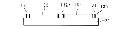
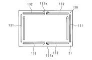
- 3A, 3B, 4A, and 4B are explanatory views illustrating a manufacturing process of the display device.
- 3A and 4A are side views
- FIGS. 4B and 4B are plan views.
- a hot-melt adhesive 130 melted so as to have a predetermined height is dropped onto the light guide plate 21.
- the dropping device When the adhesive 130 is dropped, the dropping device is scanned in the direction indicated by the white arrow in FIG. 3B along the respective short sides of the two short sides of the light guide plate 21 so that the adhesive 130 is continuously applied. Dripping into. Thereby, the short side adhesive layer 131 is formed, and the short side spacer 31 is formed by solidifying the short side adhesive layer 131.
- the agent 130 is dripped continuously. Thereby, the long side adhesive layer 132 is formed, and the long side spacer 32 is formed by solidifying the long side adhesive layer 132.
- the dropping device reads a dot pattern of the light guide plate 21 by a sensor, automatically determines a start point and an end point by processing of the CPU, and linearly scans. Further, the dropping device that moves along the long side scans up to the center of the long side, then changes the traveling direction in the outward direction of the light guide plate 21, and stops after slightly scanning. As a result, a gap 132a is formed at the center of the long side, and a gap 32a is formed in a portion corresponding to the gap 132a due to solidification of the long side adhesive layer 132.
- the spacer 30 can be accurately formed at a predetermined position without being displaced. Moreover, when this arrange
- the diffusion sheet 23 and the prism sheet 24 are arranged on one wide surface of the light guide plate 21.
- the diffusion sheet 23 and the prism sheet 24 are laminated on one wide surface of the light guide plate 21 as shown in FIGS. 4A and 4B.
- the convex portion 23a and the convex portion 24a are inserted into the gap 132a, respectively. Thereby, the diffusion sheet 23 and the prism sheet 24 can be positioned accurately.
- the liquid crystal panel 10 is placed on the short side adhesive layer 131 and the long side adhesive layer 132.
- the spacer 30 is formed, and the liquid crystal panel 10 and the light guide plate 21 are combined.
- the display device 1 is manufactured by carrying the object in which the liquid crystal panel 10 and the light guide plate 21 are combined and the light source 41 into the backlight chassis 12 and covering and fixing the bezel 11.
- the position of the spacer is difficult to determine and positioning is difficult.
- the spacer 30 is formed by scanning the dropping device and dropping the adhesive 130, the formation of the spacer 30 is automated and the spacer 30 is accurately arranged at a predetermined position.
- the diffusion sheet 23 and the prism sheet 24 can be accurately arranged. Thereby, the manufacturing cost of the display apparatus 1 can be reduced.
- the adhesive 130 When the adhesive 130 is solidified after the liquid crystal panel 10 is placed, the liquid crystal panel 10 and the light guide plate 21 are combined. Further, since the adhesive 130 is solidified between the liquid crystal panel 10 and the light guide plate 21, it also functions as the spacer 30. Thereby, the number of parts of manufacture of the display apparatus 1 can be reduced, and cost falls.
- the liquid crystal panel 10 and the light guide plate 21 are combined by solidifying the adhesive at room temperature. Therefore, the liquid crystal panel 10 and the light guide plate 21 can be combined without performing the solidifying step of the adhesive 130 in particular.
- the adhesive 130 may be dropped by a dropping device so that the surface is flattened using a squeegee.
- the spacer 30 does not need to be formed continuously, and may be formed in a dot shape along each of the four sides of the diffusion sheet 23 and the prism sheet 24, for example.
- the spacer 30 is formed of a single layer, it may be formed of a plurality of layers stacked in the facing direction of the display panel 10 and the light guide plate 21.
- the spacer 30 formed of a single layer or a plurality of layers may be formed using a UV curable resin instead of the hot melt adhesive 130.
- the spacer which consists of multiple layers using UV curable resin
- liquid UV curable resin is dripped at the light-guide plate 21 with a dripping apparatus.
- the UV curable resin dropped on the light guide plate 21 is irradiated with UV light and solidified. Thereby, a partial layer of the spacer 30 is formed.
- the diffusion sheet 23 and the prism sheet 24 are laminated on one wide surface of the light guide plate 21 in the inner space of a part of the layers of the spacer 30. Further, a UV curable resin is further dropped onto a part of the layer of the spacer 30 by a dropping device, and the liquid crystal panel 10 is placed. After the liquid crystal panel 10 is placed, the dropped UV curable resin is irradiated with UV light and solidified.
- the diffusion sheet 23 and the prism sheet 24 are laminated on the light guide plate 21, the liquid crystal panel 10 is placed on the spacer 30, and the spacer 30 is placed on the light guide plate 21. You may fix by other than. Similarly in this case, the diffusion sheet 23 or the prism sheet 24 does not come into contact with the UV curable resin due to misalignment during the manufacture of the display device 1 and is not fixed unintentionally.
- the spacer 30 may be formed by bonding the panel 10 and the light guide plate 21 with an adhesive made of a thermosetting resin or an adhesive made of an epoxy resin using a hardener.
- Display device 10 Liquid crystal panel (display panel) 21 Light guide plate 23 Diffusion sheet (optical sheet) 24 Prism sheet (optical sheet) 23a, 24a Convex part 30 Spacer 32a Gap 130 Adhesive
Landscapes
- Physics & Mathematics (AREA)
- General Physics & Mathematics (AREA)
- Optics & Photonics (AREA)
- Nonlinear Science (AREA)
- Engineering & Computer Science (AREA)
- Manufacturing & Machinery (AREA)
- Mathematical Physics (AREA)
- Chemical & Material Sciences (AREA)
- Crystallography & Structural Chemistry (AREA)
- Liquid Crystal (AREA)
- Devices For Indicating Variable Information By Combining Individual Elements (AREA)
Abstract
Description
10 液晶パネル(表示パネル)
21 導光板
23 拡散シート(光学シート)
24 プリズムシート(光学シート)
23a,24a 凸部
30 スペーサ
32a 空隙
130 接着剤
Claims (10)
- 一面に画像を表示する表示パネルと、該表示パネルの他面に対向配置された導光板と、前記表示パネル及び導光板の間に介装された光学シートと、前記表示パネル及び導光板に挟まれ、該光学シートを介装するための空間を確保するスペーサとを備える表示装置において、
前記スペーサは、前記導光板と前記表示パネルとに固着されていることを特徴とする表示装置。 - 前記光学シートには、周縁に凸部が設けられ、
前記スペーサは、前記光学シートを囲うように設けられ、前記凸部が挿入される空隙を有することを特徴とする請求項1に記載の表示装置。 - 前記スペーサは、前記表示パネル及び導光板の対向方向に積層された複数の層からなることを特徴とする請求項1又は2に記載の表示装置。
- 請求項1又は2に記載の表示装置の製造方法であって、
前記導光板に液体を滴下する滴下工程と、
滴下された前記液体に前記表示パネルを載置する載置工程と、
前記表示パネルを載置した後、前記液体を固化させる固化工程とを有し、
前記液体の固化により前記スペーサを形成すること
を特徴とする表示装置の製造方法。 - 請求項1又は2に記載の表示装置の製造方法であって、
前記導光板に溶融したホットメルト系の接着剤を滴下する滴下工程と、
前記接着剤が固化する前に、滴下された前記接着剤に前記表示パネルを載置する載置工程とを有し、
前記接着剤の固化により前記スペーサを形成すること
を特徴とする表示装置の製造方法。 - 前記滴下工程後、前記載置工程前に、前記光学シートを前記導光板に積層する積層工程を更に有することを特徴とする請求項4又は5に記載の表示装置の製造方法。
- 請求項1又は2に記載の表示装置の製造方法であって、
前記導光板に液体を滴下し、該液体を固化させることにより、前記スペーサを形成する形成工程と、
該形成工程後、前記光学シートを前記導光板に積層する積層工程とを有すること
を特徴とする表示装置の製造方法。 - 請求項3に記載の表示装置の製造方法であって、
前記導光板への液体の滴下及び該液体の固化を繰り返すことにより前記スペーサの前記複数の層を形成する形成工程と、
該形成工程の間に、前記複数の層の一部が形成された後、前記光学シートを前記導光板に積層する積層工程とを有すること
を特徴とする表示装置の製造方法。 - 前記形成工程の間にて、前記積層工程後、最後に滴下した前記液体の固化前に、該液体上に前記表示パネルを載置する載置工程を有すること
を特徴とする請求項8に記載の表示装置の製造方法。 - 一面に画像を表示する表示パネルと、該表示パネルの他面に対向配置された導光板と、前記表示パネル及び導光板の間に介装された光学シートと、前記表示パネル及び導光板に挟まれ、該光学シートを介装するための空間を確保するスペーサとを備える表示装置の製造方法において、
前記導光板に液体を滴下し、該液体の固化により前記スペーサを形成することを特徴とする表示装置の製造方法。
Priority Applications (4)
| Application Number | Priority Date | Filing Date | Title |
|---|---|---|---|
| JP2015510549A JP5945070B1 (ja) | 2014-09-26 | 2014-09-26 | 表示装置及び表示装置の製造方法 |
| PCT/JP2014/075697 WO2016046974A1 (ja) | 2014-09-26 | 2014-09-26 | 表示装置及び表示装置の製造方法 |
| CN201480002328.5A CN105765448A (zh) | 2014-09-26 | 2014-09-26 | 显示装置以及显示装置的制造方法 |
| US14/423,979 US9709726B2 (en) | 2014-09-26 | 2014-09-26 | Display apparatus and method of manufacturing the display apparatus |
Applications Claiming Priority (1)
| Application Number | Priority Date | Filing Date | Title |
|---|---|---|---|
| PCT/JP2014/075697 WO2016046974A1 (ja) | 2014-09-26 | 2014-09-26 | 表示装置及び表示装置の製造方法 |
Publications (1)
| Publication Number | Publication Date |
|---|---|
| WO2016046974A1 true WO2016046974A1 (ja) | 2016-03-31 |
Family
ID=55580533
Family Applications (1)
| Application Number | Title | Priority Date | Filing Date |
|---|---|---|---|
| PCT/JP2014/075697 Ceased WO2016046974A1 (ja) | 2014-09-26 | 2014-09-26 | 表示装置及び表示装置の製造方法 |
Country Status (4)
| Country | Link |
|---|---|
| US (1) | US9709726B2 (ja) |
| JP (1) | JP5945070B1 (ja) |
| CN (1) | CN105765448A (ja) |
| WO (1) | WO2016046974A1 (ja) |
Families Citing this family (8)
| Publication number | Priority date | Publication date | Assignee | Title |
|---|---|---|---|---|
| CN104298000B (zh) * | 2014-10-10 | 2017-04-05 | 合肥京东方光电科技有限公司 | 背光源和显示装置 |
| KR102019509B1 (ko) * | 2016-09-05 | 2019-09-09 | 엘지전자 주식회사 | 디스플레이 디바이스 |
| KR102343413B1 (ko) * | 2017-07-19 | 2021-12-24 | 삼성디스플레이 주식회사 | 표시 장치 및 그 제조 방법 |
| KR102531351B1 (ko) * | 2017-11-20 | 2023-05-11 | 삼성디스플레이 주식회사 | 광학 부재 및 이를 포함하는 표시 장치 |
| KR20190083384A (ko) * | 2018-01-03 | 2019-07-12 | 삼성디스플레이 주식회사 | 표시 장치 및 그 제조 방법 |
| CN110609412A (zh) * | 2018-06-15 | 2019-12-24 | 夏普株式会社 | 照明装置、显示装置 |
| DE102021204507B3 (de) | 2021-05-05 | 2022-09-29 | Continental Automotive Technologies GmbH | Baugruppe für eine Hintergrundbeleuchtung eines Displays und Display mit einer Hintergrundbeleuchtung mit einer solchen Baugruppe |
| CN115390309B (zh) | 2021-05-24 | 2025-05-06 | 合肥鑫晟光电科技有限公司 | 背光模组、显示面板、显示装置 |
Citations (4)
| Publication number | Priority date | Publication date | Assignee | Title |
|---|---|---|---|---|
| JP2007232809A (ja) * | 2006-02-28 | 2007-09-13 | Casio Comput Co Ltd | 表示モジュール |
| JP2010020318A (ja) * | 2008-07-14 | 2010-01-28 | Samsung Electronics Co Ltd | 液晶表示装置 |
| JP2014026293A (ja) * | 2013-10-22 | 2014-02-06 | Kyoritsu Kagaku Sangyo Kk | 表示パネルの製造方法及び表示パネル |
| JP2014142614A (ja) * | 2013-01-24 | 2014-08-07 | Lg Display Co Ltd | 液晶表示装置 |
Family Cites Families (6)
| Publication number | Priority date | Publication date | Assignee | Title |
|---|---|---|---|---|
| KR101291798B1 (ko) * | 2008-06-10 | 2013-07-31 | 엘지디스플레이 주식회사 | 액정표시모듈 및 그 조립방법 |
| CN201853028U (zh) * | 2010-11-09 | 2011-06-01 | 华映视讯(吴江)有限公司 | 一种具有膜片定位功能的液晶模组结构 |
| JP5983031B2 (ja) * | 2011-08-17 | 2016-08-31 | セイコーエプソン株式会社 | 液晶表示装置および電子機器 |
| WO2013047366A1 (ja) * | 2011-09-30 | 2013-04-04 | シャープ株式会社 | 表示装置及びテレビ受信装置 |
| TWI547740B (zh) * | 2012-11-08 | 2016-09-01 | 友達光電股份有限公司 | 具遮光模組之背光模組以及使用此背光模組的顯示裝置 |
| CN103148416B (zh) * | 2013-03-21 | 2015-01-07 | 京东方科技集团股份有限公司 | 一种背光模组及液晶显示装置 |
-
2014
- 2014-09-26 JP JP2015510549A patent/JP5945070B1/ja not_active Expired - Fee Related
- 2014-09-26 WO PCT/JP2014/075697 patent/WO2016046974A1/ja not_active Ceased
- 2014-09-26 CN CN201480002328.5A patent/CN105765448A/zh active Pending
- 2014-09-26 US US14/423,979 patent/US9709726B2/en not_active Expired - Fee Related
Patent Citations (4)
| Publication number | Priority date | Publication date | Assignee | Title |
|---|---|---|---|---|
| JP2007232809A (ja) * | 2006-02-28 | 2007-09-13 | Casio Comput Co Ltd | 表示モジュール |
| JP2010020318A (ja) * | 2008-07-14 | 2010-01-28 | Samsung Electronics Co Ltd | 液晶表示装置 |
| JP2014142614A (ja) * | 2013-01-24 | 2014-08-07 | Lg Display Co Ltd | 液晶表示装置 |
| JP2014026293A (ja) * | 2013-10-22 | 2014-02-06 | Kyoritsu Kagaku Sangyo Kk | 表示パネルの製造方法及び表示パネル |
Also Published As
| Publication number | Publication date |
|---|---|
| US20160259121A1 (en) | 2016-09-08 |
| CN105765448A (zh) | 2016-07-13 |
| JPWO2016046974A1 (ja) | 2017-04-27 |
| US9709726B2 (en) | 2017-07-18 |
| JP5945070B1 (ja) | 2016-07-05 |
Similar Documents
| Publication | Publication Date | Title |
|---|---|---|
| JP5945070B1 (ja) | 表示装置及び表示装置の製造方法 | |
| CN101493581B (zh) | 立体图像显示装置及其制造方法 | |
| KR101818138B1 (ko) | 디스플레이 장치 | |
| US20130263488A1 (en) | Display device and assembly method thereof | |
| JP4494446B2 (ja) | 表示装置 | |
| JP4981944B2 (ja) | 液晶表示装置用セルの製造方法 | |
| JP2013073184A5 (ja) | ||
| WO2019144460A1 (zh) | 显示模组及其制备方法和显示装置 | |
| JP2017120310A (ja) | 表示装置、表示装置に用いる接着シート、および表示装置の製造方法 | |
| JP6456473B2 (ja) | 表示装置の製造方法 | |
| JP5162834B2 (ja) | 表示モジュール | |
| CN104965344A (zh) | 液晶显示装置及其导光板的制造方法 | |
| JP5705701B2 (ja) | 液晶表示装置 | |
| TW200528883A (en) | Liquid crystal display apparatus and method for manufacturing the same | |
| US10203450B2 (en) | Backlight module and the manufacturing method thereof | |
| KR20130039463A (ko) | 백라이트유니트용 복합시트 및 그 제조 방법 | |
| CN203375279U (zh) | 定位组件、背光模组及显示装置 | |
| JP5946419B2 (ja) | 液晶表示装置の製造方法 | |
| CN100365484C (zh) | 光学膜片总成和该光学膜片的加工方法及加工装置 | |
| TWI414429B (zh) | 防溢膠裝置及使用其之基板貼合方法 | |
| JP7827290B2 (ja) | 表示装置 | |
| CN103901662B (zh) | 一种窄边框液晶模组 | |
| JP2011180483A (ja) | 液晶表示装置および電子機器 | |
| US20110212309A1 (en) | Optical film assembly and manufacturing method and manufacturing apparatus for producing the same | |
| JP6845631B2 (ja) | 表示装置の組立方法 |
Legal Events
| Date | Code | Title | Description |
|---|---|---|---|
| ENP | Entry into the national phase |
Ref document number: 2015510549 Country of ref document: JP Kind code of ref document: A |
|
| WWE | Wipo information: entry into national phase |
Ref document number: 14423979 Country of ref document: US |
|
| 121 | Ep: the epo has been informed by wipo that ep was designated in this application |
Ref document number: 14902819 Country of ref document: EP Kind code of ref document: A1 |
|
| NENP | Non-entry into the national phase |
Ref country code: DE |
|
| 122 | Ep: pct application non-entry in european phase |
Ref document number: 14902819 Country of ref document: EP Kind code of ref document: A1 |