WO2016013310A1 - シート状樹脂組成物、裏面研削用テープ一体型シート状樹脂組成物、及び、半導体装置の製造方法 - Google Patents
シート状樹脂組成物、裏面研削用テープ一体型シート状樹脂組成物、及び、半導体装置の製造方法 Download PDFInfo
- Publication number
- WO2016013310A1 WO2016013310A1 PCT/JP2015/066293 JP2015066293W WO2016013310A1 WO 2016013310 A1 WO2016013310 A1 WO 2016013310A1 JP 2015066293 W JP2015066293 W JP 2015066293W WO 2016013310 A1 WO2016013310 A1 WO 2016013310A1
- Authority
- WO
- WIPO (PCT)
- Prior art keywords
- sheet
- resin composition
- shaped resin
- thermosetting
- heating
- Prior art date
- Legal status (The legal status is an assumption and is not a legal conclusion. Google has not performed a legal analysis and makes no representation as to the accuracy of the status listed.)
- Ceased
Links
Images





Classifications
-
- B—PERFORMING OPERATIONS; TRANSPORTING
- B32—LAYERED PRODUCTS
- B32B—LAYERED PRODUCTS, i.e. PRODUCTS BUILT-UP OF STRATA OF FLAT OR NON-FLAT, e.g. CELLULAR OR HONEYCOMB, FORM
- B32B7/00—Layered products characterised by the relation between layers; Layered products characterised by the relative orientation of features between layers, or by the relative values of a measurable parameter between layers, i.e. products comprising layers having different physical, chemical or physicochemical properties; Layered products characterised by the interconnection of layers
- B32B7/02—Physical, chemical or physicochemical properties
- B32B7/027—Thermal properties
-
- B—PERFORMING OPERATIONS; TRANSPORTING
- B32—LAYERED PRODUCTS
- B32B—LAYERED PRODUCTS, i.e. PRODUCTS BUILT-UP OF STRATA OF FLAT OR NON-FLAT, e.g. CELLULAR OR HONEYCOMB, FORM
- B32B27/00—Layered products comprising a layer of synthetic resin
- B32B27/38—Layered products comprising a layer of synthetic resin comprising epoxy resins
-
- C—CHEMISTRY; METALLURGY
- C08—ORGANIC MACROMOLECULAR COMPOUNDS; THEIR PREPARATION OR CHEMICAL WORKING-UP; COMPOSITIONS BASED THEREON
- C08G—MACROMOLECULAR COMPOUNDS OBTAINED OTHERWISE THAN BY REACTIONS ONLY INVOLVING UNSATURATED CARBON-TO-CARBON BONDS
- C08G59/00—Polycondensates containing more than one epoxy group per molecule; Macromolecules obtained by polymerising compounds containing more than one epoxy group per molecule using curing agents or catalysts which react with the epoxy groups
- C08G59/18—Macromolecules obtained by polymerising compounds containing more than one epoxy group per molecule using curing agents or catalysts which react with the epoxy groups ; e.g. general methods of curing
- C08G59/40—Macromolecules obtained by polymerising compounds containing more than one epoxy group per molecule using curing agents or catalysts which react with the epoxy groups ; e.g. general methods of curing characterised by the curing agents used
- C08G59/66—Mercaptans
-
- C—CHEMISTRY; METALLURGY
- C08—ORGANIC MACROMOLECULAR COMPOUNDS; THEIR PREPARATION OR CHEMICAL WORKING-UP; COMPOSITIONS BASED THEREON
- C08J—WORKING-UP; GENERAL PROCESSES OF COMPOUNDING; AFTER-TREATMENT NOT COVERED BY SUBCLASSES C08B, C08C, C08F, C08G or C08H
- C08J5/00—Manufacture of articles or shaped materials containing macromolecular substances
- C08J5/18—Manufacture of films or sheets
-
- C—CHEMISTRY; METALLURGY
- C08—ORGANIC MACROMOLECULAR COMPOUNDS; THEIR PREPARATION OR CHEMICAL WORKING-UP; COMPOSITIONS BASED THEREON
- C08L—COMPOSITIONS OF MACROMOLECULAR COMPOUNDS
- C08L101/00—Compositions of unspecified macromolecular compounds
-
- C—CHEMISTRY; METALLURGY
- C08—ORGANIC MACROMOLECULAR COMPOUNDS; THEIR PREPARATION OR CHEMICAL WORKING-UP; COMPOSITIONS BASED THEREON
- C08L—COMPOSITIONS OF MACROMOLECULAR COMPOUNDS
- C08L33/00—Compositions of homopolymers or copolymers of compounds having one or more unsaturated aliphatic radicals, each having only one carbon-to-carbon double bond, and only one being terminated by only one carboxyl radical, or of salts, anhydrides, esters, amides, imides or nitriles thereof; Compositions of derivatives of such polymers
- C08L33/04—Homopolymers or copolymers of esters
- C08L33/06—Homopolymers or copolymers of esters of esters containing only carbon, hydrogen and oxygen, which oxygen atoms are present only as part of the carboxyl radical
- C08L33/062—Copolymers with monomers not covered by C08L33/06
- C08L33/068—Copolymers with monomers not covered by C08L33/06 containing glycidyl groups
-
- C—CHEMISTRY; METALLURGY
- C08—ORGANIC MACROMOLECULAR COMPOUNDS; THEIR PREPARATION OR CHEMICAL WORKING-UP; COMPOSITIONS BASED THEREON
- C08L—COMPOSITIONS OF MACROMOLECULAR COMPOUNDS
- C08L63/00—Compositions of epoxy resins; Compositions of derivatives of epoxy resins
-
- C—CHEMISTRY; METALLURGY
- C09—DYES; PAINTS; POLISHES; NATURAL RESINS; ADHESIVES; COMPOSITIONS NOT OTHERWISE PROVIDED FOR; APPLICATIONS OF MATERIALS NOT OTHERWISE PROVIDED FOR
- C09J—ADHESIVES; NON-MECHANICAL ASPECTS OF ADHESIVE PROCESSES IN GENERAL; ADHESIVE PROCESSES NOT PROVIDED FOR ELSEWHERE; USE OF MATERIALS AS ADHESIVES
- C09J11/00—Features of adhesives not provided for in group C09J9/00, e.g. additives
- C09J11/02—Non-macromolecular additives
- C09J11/06—Non-macromolecular additives organic
-
- C—CHEMISTRY; METALLURGY
- C09—DYES; PAINTS; POLISHES; NATURAL RESINS; ADHESIVES; COMPOSITIONS NOT OTHERWISE PROVIDED FOR; APPLICATIONS OF MATERIALS NOT OTHERWISE PROVIDED FOR
- C09J—ADHESIVES; NON-MECHANICAL ASPECTS OF ADHESIVE PROCESSES IN GENERAL; ADHESIVE PROCESSES NOT PROVIDED FOR ELSEWHERE; USE OF MATERIALS AS ADHESIVES
- C09J133/00—Adhesives based on homopolymers or copolymers of compounds having one or more unsaturated aliphatic radicals, each having only one carbon-to-carbon double bond, and at least one being terminated by only one carboxyl radical, or of salts, anhydrides, esters, amides, imides, or nitriles thereof; Adhesives based on derivatives of such polymers
-
- C—CHEMISTRY; METALLURGY
- C09—DYES; PAINTS; POLISHES; NATURAL RESINS; ADHESIVES; COMPOSITIONS NOT OTHERWISE PROVIDED FOR; APPLICATIONS OF MATERIALS NOT OTHERWISE PROVIDED FOR
- C09J—ADHESIVES; NON-MECHANICAL ASPECTS OF ADHESIVE PROCESSES IN GENERAL; ADHESIVE PROCESSES NOT PROVIDED FOR ELSEWHERE; USE OF MATERIALS AS ADHESIVES
- C09J163/00—Adhesives based on epoxy resins; Adhesives based on derivatives of epoxy resins
-
- C—CHEMISTRY; METALLURGY
- C09—DYES; PAINTS; POLISHES; NATURAL RESINS; ADHESIVES; COMPOSITIONS NOT OTHERWISE PROVIDED FOR; APPLICATIONS OF MATERIALS NOT OTHERWISE PROVIDED FOR
- C09J—ADHESIVES; NON-MECHANICAL ASPECTS OF ADHESIVE PROCESSES IN GENERAL; ADHESIVE PROCESSES NOT PROVIDED FOR ELSEWHERE; USE OF MATERIALS AS ADHESIVES
- C09J201/00—Adhesives based on unspecified macromolecular compounds
-
- C—CHEMISTRY; METALLURGY
- C09—DYES; PAINTS; POLISHES; NATURAL RESINS; ADHESIVES; COMPOSITIONS NOT OTHERWISE PROVIDED FOR; APPLICATIONS OF MATERIALS NOT OTHERWISE PROVIDED FOR
- C09J—ADHESIVES; NON-MECHANICAL ASPECTS OF ADHESIVE PROCESSES IN GENERAL; ADHESIVE PROCESSES NOT PROVIDED FOR ELSEWHERE; USE OF MATERIALS AS ADHESIVES
- C09J7/00—Adhesives in the form of films or foils
- C09J7/10—Adhesives in the form of films or foils without carriers
-
- C—CHEMISTRY; METALLURGY
- C09—DYES; PAINTS; POLISHES; NATURAL RESINS; ADHESIVES; COMPOSITIONS NOT OTHERWISE PROVIDED FOR; APPLICATIONS OF MATERIALS NOT OTHERWISE PROVIDED FOR
- C09J—ADHESIVES; NON-MECHANICAL ASPECTS OF ADHESIVE PROCESSES IN GENERAL; ADHESIVE PROCESSES NOT PROVIDED FOR ELSEWHERE; USE OF MATERIALS AS ADHESIVES
- C09J7/00—Adhesives in the form of films or foils
- C09J7/20—Adhesives in the form of films or foils characterised by their carriers
-
- C—CHEMISTRY; METALLURGY
- C09—DYES; PAINTS; POLISHES; NATURAL RESINS; ADHESIVES; COMPOSITIONS NOT OTHERWISE PROVIDED FOR; APPLICATIONS OF MATERIALS NOT OTHERWISE PROVIDED FOR
- C09J—ADHESIVES; NON-MECHANICAL ASPECTS OF ADHESIVE PROCESSES IN GENERAL; ADHESIVE PROCESSES NOT PROVIDED FOR ELSEWHERE; USE OF MATERIALS AS ADHESIVES
- C09J7/00—Adhesives in the form of films or foils
- C09J7/20—Adhesives in the form of films or foils characterised by their carriers
- C09J7/22—Plastics; Metallised plastics
- C09J7/24—Plastics; Metallised plastics based on macromolecular compounds obtained by reactions involving only carbon-to-carbon unsaturated bonds
- C09J7/245—Vinyl resins, e.g. polyvinyl chloride [PVC]
-
- H—ELECTRICITY
- H10—SEMICONDUCTOR DEVICES; ELECTRIC SOLID-STATE DEVICES NOT OTHERWISE PROVIDED FOR
- H10P—GENERIC PROCESSES OR APPARATUS FOR THE MANUFACTURE OR TREATMENT OF DEVICES COVERED BY CLASS H10
- H10P52/00—Grinding, lapping or polishing of wafers, substrates or parts of devices
-
- H—ELECTRICITY
- H10—SEMICONDUCTOR DEVICES; ELECTRIC SOLID-STATE DEVICES NOT OTHERWISE PROVIDED FOR
- H10P—GENERIC PROCESSES OR APPARATUS FOR THE MANUFACTURE OR TREATMENT OF DEVICES COVERED BY CLASS H10
- H10P90/00—Preparation of wafers not covered by a single main group of this subclass, e.g. wafer reinforcement
- H10P90/12—Preparing bulk and homogeneous wafers
- H10P90/123—Preparing bulk and homogeneous wafers by grinding or lapping
-
- H—ELECTRICITY
- H10—SEMICONDUCTOR DEVICES; ELECTRIC SOLID-STATE DEVICES NOT OTHERWISE PROVIDED FOR
- H10W—GENERIC PACKAGES, INTERCONNECTIONS, CONNECTORS OR OTHER CONSTRUCTIONAL DETAILS OF DEVICES COVERED BY CLASS H10
- H10W72/00—Interconnections or connectors in packages
- H10W72/01—Manufacture or treatment
- H10W72/013—Manufacture or treatment of die-attach connectors
-
- H—ELECTRICITY
- H10—SEMICONDUCTOR DEVICES; ELECTRIC SOLID-STATE DEVICES NOT OTHERWISE PROVIDED FOR
- H10W—GENERIC PACKAGES, INTERCONNECTIONS, CONNECTORS OR OTHER CONSTRUCTIONAL DETAILS OF DEVICES COVERED BY CLASS H10
- H10W74/00—Encapsulations, e.g. protective coatings
- H10W74/01—Manufacture or treatment
-
- H—ELECTRICITY
- H10—SEMICONDUCTOR DEVICES; ELECTRIC SOLID-STATE DEVICES NOT OTHERWISE PROVIDED FOR
- H10W—GENERIC PACKAGES, INTERCONNECTIONS, CONNECTORS OR OTHER CONSTRUCTIONAL DETAILS OF DEVICES COVERED BY CLASS H10
- H10W72/00—Interconnections or connectors in packages
- H10W72/01—Manufacture or treatment
- H10W72/012—Manufacture or treatment of bump connectors, dummy bumps or thermal bumps
- H10W72/01271—Cleaning, e.g. oxide removal or de-smearing
-
- H—ELECTRICITY
- H10—SEMICONDUCTOR DEVICES; ELECTRIC SOLID-STATE DEVICES NOT OTHERWISE PROVIDED FOR
- H10W—GENERIC PACKAGES, INTERCONNECTIONS, CONNECTORS OR OTHER CONSTRUCTIONAL DETAILS OF DEVICES COVERED BY CLASS H10
- H10W72/00—Interconnections or connectors in packages
- H10W72/071—Connecting or disconnecting
- H10W72/072—Connecting or disconnecting of bump connectors
-
- H—ELECTRICITY
- H10—SEMICONDUCTOR DEVICES; ELECTRIC SOLID-STATE DEVICES NOT OTHERWISE PROVIDED FOR
- H10W—GENERIC PACKAGES, INTERCONNECTIONS, CONNECTORS OR OTHER CONSTRUCTIONAL DETAILS OF DEVICES COVERED BY CLASS H10
- H10W72/00—Interconnections or connectors in packages
- H10W72/071—Connecting or disconnecting
- H10W72/073—Connecting or disconnecting of die-attach connectors
-
- H—ELECTRICITY
- H10—SEMICONDUCTOR DEVICES; ELECTRIC SOLID-STATE DEVICES NOT OTHERWISE PROVIDED FOR
- H10W—GENERIC PACKAGES, INTERCONNECTIONS, CONNECTORS OR OTHER CONSTRUCTIONAL DETAILS OF DEVICES COVERED BY CLASS H10
- H10W74/00—Encapsulations, e.g. protective coatings
- H10W74/10—Encapsulations, e.g. protective coatings characterised by their shape or disposition
- H10W74/15—Encapsulations, e.g. protective coatings characterised by their shape or disposition on active surfaces of flip-chip devices, e.g. underfills
-
- H—ELECTRICITY
- H10—SEMICONDUCTOR DEVICES; ELECTRIC SOLID-STATE DEVICES NOT OTHERWISE PROVIDED FOR
- H10W—GENERIC PACKAGES, INTERCONNECTIONS, CONNECTORS OR OTHER CONSTRUCTIONAL DETAILS OF DEVICES COVERED BY CLASS H10
- H10W90/00—Package configurations
- H10W90/701—Package configurations characterised by the relative positions of pads or connectors relative to package parts
- H10W90/721—Package configurations characterised by the relative positions of pads or connectors relative to package parts of bump connectors
- H10W90/724—Package configurations characterised by the relative positions of pads or connectors relative to package parts of bump connectors between a chip and a stacked insulating package substrate, interposer or RDL
-
- H—ELECTRICITY
- H10—SEMICONDUCTOR DEVICES; ELECTRIC SOLID-STATE DEVICES NOT OTHERWISE PROVIDED FOR
- H10W—GENERIC PACKAGES, INTERCONNECTIONS, CONNECTORS OR OTHER CONSTRUCTIONAL DETAILS OF DEVICES COVERED BY CLASS H10
- H10W90/00—Package configurations
- H10W90/701—Package configurations characterised by the relative positions of pads or connectors relative to package parts
- H10W90/731—Package configurations characterised by the relative positions of pads or connectors relative to package parts of die-attach connectors
- H10W90/734—Package configurations characterised by the relative positions of pads or connectors relative to package parts of die-attach connectors between a chip and a stacked insulating package substrate, interposer or RDL
Definitions
- the present invention relates to a sheet-shaped resin composition, a tape-integrated sheet-shaped resin composition for back grinding, and a method for manufacturing a semiconductor device.
- an epoxy resin is often used as a thermosetting resin, and a phenol resin is often used as a curing agent.
- the present invention has been made in view of the above-described problems, and an object of the present invention is to provide a sheet-shaped resin composition that has good storage stability and has fast curability in a semiconductor device manufacturing process. Moreover, it is providing the tape-integrated sheet-like resin composition for back grinding which has the said sheet-like resin composition. Moreover, it is providing the manufacturing method of the semiconductor device using the said sheet-like resin composition.
- the present invention is a sheet-like resin composition for manufacturing a semiconductor device,
- the thermosetting rate after heating at 120 ° C. for 10 minutes is 40% or less
- the thermosetting rate after heating at 200 ° C. for 20 seconds is 50% or more.
- the thermal curing rate after heating at 120 ° C. for 10 minutes is 40% or less, and the progress of the curing reaction at a low temperature is suppressed. Therefore, it is excellent in the preservability in the state of a sheet-like resin composition.
- the thermal curing rate after heating at 200 ° C. for 20 seconds is 50% or more, the curing reaction can proceed in a short time under conditions that are not so high in the curing reaction in the semiconductor device manufacturing process. . As a result, manufacturing efficiency can be improved.
- the sheet-shaped resin composition according to the present invention it is possible to provide a sheet-shaped resin composition that has good storage stability and has fast curability in the manufacturing process of a semiconductor device.
- thermosetting rate is a value obtained from reaction heat obtained by differential scanning calorimetry (DSC), assuming that the state before heating is 0% and the state of complete thermosetting is 100%. More details will be described later.
- an epoxy (meth) acrylate resin and a radical generator are included.
- the radical generator hardly generates radicals unless the conditions for generating radicals are satisfied, and generates radicals when the conditions for generating radicals are satisfied.
- the epoxy (meth) acrylate resin has a carbon-carbon double bond.
- this radical addition reaction proceeds in a chain manner. Accordingly, when a radical generator that does not generate radicals at room temperature (for example, 120 ° C.
- the epoxy (meth) acrylate resin does not need to have an epoxy group that reacts with the curing agent. However, a very small amount of epoxy groups may remain, for example, when an epoxy (meth) acrylate resin is produced by an ester reaction of diglycidyl ether and (meth) acrylic acid.
- the epoxy (meth) acrylate resin does not need to have an epoxy group to the extent that it contributes as a curing reaction.
- the oxirane oxygen concentration may be 0.2% by weight or less.
- curing agent are contained, the said thermosetting resin is an epoxy resin, and the said hardening
- the thiol-based curing agent generally has a narrow temperature range from the curing start temperature to the curing end temperature, as compared with the phenol resin. Therefore, if a thiol-based curing agent is used as the curing agent for the epoxy resin, the thermal curing rate after heating at 120 ° C. for 10 minutes is 40% or less, and the thermal curing rate after heating at 200 ° C. for 20 seconds is 50 % Or more.
- thermoplastic resin is contained and the said thermoplastic resin is an acrylic resin whose weight average molecular weight is 3x10 ⁇ 5 > or more.
- the resin composition is easily formed into a sheet.
- the back-grinding tape-integrated sheet-shaped resin composition according to the present invention is characterized in that the sheet-shaped resin composition is laminated on the back-grinding tape.
- the sheet-shaped resin composition has a thermosetting rate of 40% or less after heating at 120 ° C. for 10 minutes and a thermosetting rate of 50% or more after heating at 200 ° C. for 20 seconds. And has a fast curability in the semiconductor device manufacturing process.
- a method for manufacturing a semiconductor device includes: Step A for preparing a chip with a sheet-shaped resin composition in which the sheet-shaped resin composition is attached to a bump forming surface of a semiconductor chip; Step B for preparing a mounting substrate on which electrodes are formed; The sheet-shaped resin composition-attached chip is attached to the mounting substrate with the sheet-shaped resin composition as a bonding surface, and the bumps formed on the semiconductor chip and the mounting substrate are formed.
- Step C for making the electrodes face each other; After the step C, the step D of heating and semi-curing the sheet-shaped resin composition, After the step D, the method includes a step E of heating at a higher temperature than the heating in the step D to join the bump and the electrode and curing the sheet-like composition.
- the thermal curing rate after heating at 120 ° C. for 10 minutes is 40% or less, and the thermal curing rate after heating at 200 ° C. for 20 seconds is 50% or more. Since the sheet-like resin composition is used, the curing reaction starts and ends early even if the temperature is not greatly increased after the process C until the semi-curing process of the process D. Since the process D can be completed quickly, the efficiency of the semiconductor device manufacturing process can be improved.
- the present invention it is possible to provide a sheet-shaped resin composition which has good storage stability and has fast curability in a semiconductor device manufacturing process. Moreover, the tape-integrated sheet-like resin composition for back surface grinding which has the said sheet-like resin composition can be provided. Moreover, the manufacturing method of the semiconductor device using the said sheet-like resin composition can be provided.
- FIG. 1 is a schematic cross-sectional view showing a back-grinding tape-integrated sheet-shaped resin composition according to an embodiment of the present invention.
- the back-grinding tape-integrated sheet-shaped resin composition 100 includes a back-grinding tape 12 and a sheet-shaped resin composition 10 laminated on the back-grinding tape 12. Is provided.
- the back grinding tape 12 includes a substrate 12a and an adhesive layer 12b, and the adhesive layer 12b is provided on the substrate 12a.
- the sheet-like resin composition 10 is provided on the pressure-sensitive adhesive layer 12b.
- the sheet-shaped resin composition 10 does not have to be laminated on the entire surface of the back surface grinding tape 12 as shown in FIG. 1, and has a size sufficient for bonding to the semiconductor wafer 16 (see FIG. 2). What is necessary is just to be provided.
- the sheet-shaped resin composition 10 has a function of sealing a gap between the semiconductor chip 22 and the mounting substrate 50 when the semiconductor chip 22 is mounted on the mounting substrate 50 (see FIG. 9).
- the sheet-like resin composition 10 has a thermosetting rate of 40% or less after heating at 120 ° C. for 10 minutes, preferably 35% or less, and more preferably 30% or less.
- the sheet-like resin composition 10 has a thermosetting rate of 40% or less after being heated at 120 ° C. for 10 minutes, and the progress of the curing reaction at a low temperature is suppressed. Therefore, it is excellent in the preservability in the state of a sheet-like resin composition.
- the sheet-like resin composition 10 has a thermosetting rate of 50% or more after heating at 200 ° C. for 20 seconds, preferably 60% or more, and more preferably 70% or more. Since the sheet-shaped resin composition 10 has a thermal curing rate of 50% or more after being heated at 200 ° C.
- the curing reaction in a curing reaction in a semiconductor device manufacturing process is not so high and in a short time. Can be advanced. As a result, manufacturing efficiency can be improved.
- the thermosetting rate after heating the sheet-like resin composition 10 at 120 ° C. for 10 minutes and the thermosetting rate after heating at 200 ° C. for 20 seconds are the types of curing agents contained in the sheet-like resin composition 10 and It can be controlled by the type of curing accelerator, the content of curing accelerator, various additives, and the like.
- thermosetting rate is obtained by measuring the calorific value using differential scanning calorimetry (DSC). Specifically, first, a sheet-shaped resin composition that has not been heat-cured is prepared, and the temperature is set to 350 ° C. (the thermosetting reaction is assumed to be completely completed from ⁇ 10 ° C. under a temperature rising rate of 10 ° C./min. The amount of heat generated when the temperature is raised to (the temperature of reaction of the uncured sample) is measured. Moreover, the sample which heated the sheet-like resin composition before thermosetting on predetermined conditions (The heating for 10 minutes at 120 degreeC or the heating for 20 seconds at 200 degreeC) is created. Next, the heat generated when the sample heated under the predetermined conditions was heated from ⁇ 10 ° C. to 350 ° C.
- DSC differential scanning calorimetry
- thermosetting rate is obtained by the following formula (1).
- the calorific value is determined using the area surrounded by the straight line connecting the two points of the rising temperature of the exothermic peak and the reaction end temperature measured with a differential scanning calorimeter and the peak.
- Thermal curing rate [ ⁇ (reaction heat amount of uncured sample) ⁇ (reaction heat amount of sample thermally cured under predetermined conditions) ⁇ / (reaction heat amount of uncured sample)] ⁇ 100 (%)
- the sheet-shaped resin composition 10 is prepared so that the peak temperature of thermosetting is within a range of 130 ° C. to 190 ° C. when measured under a temperature rising condition of 10 ° C./min in differential scanning calorimetry. preferable.
- Examples of the method for adjusting the peak temperature of thermosetting so as to be within the range of 130 ° C. to 190 ° C. include a method of adjusting depending on the type of the curing accelerator and the content of the curing accelerator.
- the sheet-like resin composition 10 preferably has a viscosity at 120 ° C. of 0.1 kPa ⁇ s to 10 kPa ⁇ s, more preferably 0.5 kPa ⁇ s to 9 kPa ⁇ s, and more preferably 1 kPa ⁇ s to 1 kPa ⁇ s. More preferably, it is 8 kPa ⁇ s or less. If the viscosity at 120 ° C. of the sheet-shaped resin composition 10 is 0.1 kPa ⁇ s or more, void expansion when the temperature is raised from the temperature in Step C to the temperature in the semi-curing step D can be suppressed. On the other hand, when it is 10 kPa ⁇ s or less, the sheet-shaped resin composition can be embedded in the unevenness of the mounting substrate.
- the sheet-like resin composition 10 has a viscosity change rate X1 between a viscosity at 120 ° C. after storage for 1 week at a temperature of 25 ° C. and a viscosity at 120 ° C. before storage in an absolute value of 0 to It is preferably in the range of 40%, more preferably in the range of 0 to 20%.
- the sheet-like resin composition 10 has a viscosity change rate X2 between the viscosity at 120 ° C. after storage for 2 weeks and the viscosity at 120 ° C. before storage at a temperature of 25 ° C. in an absolute value of 0 to It is preferably in the range of 40%, more preferably in the range of 0 to 20%.
- the sheet-like resin composition 10 preferably has a minimum melt viscosity of less than 200 ° C. within a range of 10 Pa ⁇ s to 5000 Pa ⁇ s, more preferably within a range of 50 Pa ⁇ s to 3000 Pa ⁇ s, and 100 Pa ⁇ s. More preferably, it is in the range of s to 2000 Pa ⁇ s.
- the minimum melt viscosity at less than 200 ° C. of the sheet-shaped resin composition 10 is in the range of 10 Pa ⁇ s to 5000 Pa ⁇ s
- the bump 18 formed on the semiconductor chip 22 and the mounting substrate 50 are formed in Step C described later.
- the formed electrode 52 can be opposed to the sheet-shaped resin composition 10 while being easily embedded.
- the minimum melt viscosity at less than 200 ° C. of the sheet-shaped resin composition 10 refers to the minimum melt viscosity at less than 200 ° C. before thermosetting.
- the minimum melt viscosity at less than 200 ° C. of the sheet-shaped resin composition 10 can be controlled by selecting the constituent material of the sheet-shaped resin composition 10. In particular, it can be controlled by selecting a thermoplastic resin. Specifically, for example, when a low molecular weight resin is used as the thermoplastic resin, the minimum melt viscosity at less than 200 ° C. can be reduced. For example, when a high molecular weight resin is used, the minimum melt viscosity at less than 200 ° C. Can be increased.
- the sheet-like resin composition 10 contains a thermosetting resin. Moreover, it is preferable that the sheet-like resin composition 10 contains a hardening
- thermosetting resin examples include epoxy resin, phenol resin, amino resin, unsaturated polyester resin, polyurethane resin, silicone resin, and thermosetting polyimide resin. These resins can be used alone or in combination of two or more. In particular, an epoxy resin containing a small amount of ionic impurities that corrode the semiconductor chip is preferable.
- the epoxy resin is not particularly limited as long as it is generally used as an adhesive composition, for example, bisphenol A type, bisphenol F type, bisphenol S type, brominated bisphenol A type, hydrogenated bisphenol A type, bisphenol AF type.
- a thiol-based curing agent As a curing agent, from the viewpoint of reactivity with thiol-based curing agents and versatility, among the epoxy resins, bisphenol A type, biphenyl type, naphthalene type, phenol novolac type, orthocresol novolak A mold is particularly preferred.
- the content of the thermosetting resin with respect to the entire sheet-shaped resin composition 10 is not particularly limited as long as the sheet-shaped resin composition can exhibit a function as a thermosetting sheet, and is in the range of 5 to 50% by weight. Preferably, it is within the range of 10 to 30% by weight.
- curing agent can be suitably selected according to the kind of thermosetting resin.
- the thermosetting resin is an epoxy resin
- the curing agent is preferably a thiol curing agent having two or more mercapto groups in the molecule.
- numerator is preferable.
- the thiol-based curing agent has a narrower temperature range from the curing start temperature to the curing end temperature than the phenol resin. Therefore, if a thiol-based curing agent is used as the curing agent for the epoxy resin, the thermal curing rate after heating at 120 ° C.
- thiol curing agents a thiol curing agent having one or more secondary mercapto groups in the molecule is more preferable, and a thiol curing agent having four secondary mercapto groups in the molecule is more preferable.
- a secondary mercapto group has a large steric hindrance due to the presence of a methyl group, and is less reactive with an epoxy group than a primary mercapto group.
- the secondary mercapto group can form an internal hydrogen bond with the carbonyl group at the ⁇ -position, the secondary mercapto group becomes stable and the reactivity decreases. Therefore, it is easy to make the thermosetting rate after heating the sheet-shaped resin composition 10 at 120 degreeC for 10 minutes more 40% or less.
- the thiol-based curing agents those that can make the curing temperature of the sheet-shaped resin composition 10 higher than when a phenol resin is used (for example, about 120 to 180 ° C.) are preferable.
- thiol-based curing agent examples include pentaerythritol tetrakis (3-mercaptobutyrate) represented by the following formula (2) having a secondary mercapto group in the molecule, and represented by the following formula (3).
- the blending amount of the curing agent is not particularly limited, but is preferably 5 to 30% by weight, and preferably 10 to 20% by weight with respect to the entire sheet-shaped resin composition 10. More preferred.
- the sheet-shaped resin composition 10 may contain a thermosetting accelerator.
- the thermosetting accelerator is not particularly limited and can be appropriately selected from known thermosetting accelerators.
- a thermosetting accelerator can be used individually or in combination of 2 or more types.
- the thermosetting accelerator for example, amine-based curing accelerators, phosphorus-based curing accelerators, imidazole-based curing accelerators, boron-based curing accelerators, phosphorus-boron-based curing accelerators, and the like can be used.
- organic compounds containing nitrogen atoms in the molecule for example, amine-based curing accelerators and imidazole-based curing accelerators
- the content of the thermosetting accelerator is preferably 0.3 parts by weight or more, more preferably 1.0 parts by weight or more, based on 100 parts by weight of the thermosetting resin, and 2.0% by weight. More preferably, it is at least part. When it is 4.8 parts by weight or more, the sheet-shaped resin composition 10 can be easily semi-cured in a semi-curing step (step D) described later.
- the content of the thermosetting accelerator is preferably 24 parts by weight or less. The preservability of a thermosetting resin can be improved as it is 24 weight part or less.
- the sheet-like resin composition 10 preferably contains a thermoplastic resin.
- the thermoplastic resin include natural rubber, butyl rubber, isoprene rubber, chloroprene rubber, ethylene-vinyl acetate copolymer, ethylene-acrylic acid copolymer, ethylene-acrylic acid ester copolymer, polybutadiene resin, polycarbonate resin, heat Examples thereof include plastic polyimide resins, polyamide resins such as 6-nylon and 6,6-nylon, phenoxy resins, acrylic resins, saturated polyester resins such as PET and PBT, polyamideimide resins, and fluorine resins. These thermoplastic resins can be used alone or in combination of two or more. Among these thermoplastic resins, an acrylic resin that has few ionic impurities and high heat resistance and can ensure the reliability of the semiconductor chip is particularly preferable.
- the acrylic resin is not particularly limited, and includes one or more esters of acrylic acid or methacrylic acid ester having a linear or branched alkyl group having 30 or less carbon atoms, particularly 4 to 18 carbon atoms.
- Examples include polymers as components.
- the alkyl group include methyl group, ethyl group, propyl group, isopropyl group, n-butyl group, t-butyl group, isobutyl group, amyl group, isoamyl group, hexyl group, heptyl group, cyclohexyl group, 2 -Ethylhexyl group, octyl group, isooctyl group, nonyl group, isononyl group, decyl group, isodecyl group, undecyl group, lauryl group, tridecyl group, tetradecyl group, stearyl group, octadecyl group,
- the other monomer forming the polymer is not particularly limited, and examples thereof include acrylic acid, methacrylic acid, carboxyethyl acrylate, carboxypentyl acrylate, itaconic acid, maleic acid, fumaric acid, and crotonic acid.
- Carboxyl group-containing monomers maleic anhydride or acid anhydride monomers such as itaconic anhydride, 2-hydroxyethyl (meth) acrylate, 2-hydroxypropyl (meth) acrylate, 4-methacrylic acid 4- Hydroxybutyl, 6-hydroxyhexyl (meth) acrylate, 8-hydroxyoctyl (meth) acrylate, 10-hydroxydecyl (meth) acrylate, 12-hydroxylauryl (meth) acrylate or (4-hydroxymethylcyclohexyl) -Methyl Hydroxyl group-containing monomers such as acrylate, styrene sulfonic acid, allyl sulfonic acid, 2- (meth) acrylamide-2-methylpropane sulfonic acid, (meth) acrylamide propane sulfonic acid, sulfopropyl (meth) acrylate or (meth) Examples thereof include sulfonic acid group-containing monomers such as
- the acrylic resin preferably has a weight average molecular weight of 3 ⁇ 10 5 or more, and more preferably 4 ⁇ 10 5 or more, from the viewpoint of film formability.
- the thermoplastic resin contains an acrylic resin having a weight average molecular weight of 3 ⁇ 10 5 or more, the resin composition is easily formed into a sheet.
- the weight average molecular weight is measured by GPC (gel permeation chromatography) and is a value calculated in terms of polystyrene.
- the content of the thermoplastic resin with respect to the entire sheet-shaped resin composition 10 is preferably 1% by weight or more, and more preferably 3% by weight or more. When it is 1% by weight or more, good flexibility is obtained. On the other hand, the content of the thermoplastic resin in the resin component is preferably 15% by weight or less, more preferably 12% by weight or less, and still more preferably 8% by weight or less. Good thermal reliability is acquired as it is 15 weight% or less.
- the sheet-like resin composition 10 can be appropriately mixed with an inorganic filler.
- the blending of the inorganic filler makes it possible to improve thermal conductivity, adjust the storage elastic modulus, and the like.
- the inorganic filler examples include ceramics such as silica, clay, gypsum, calcium carbonate, barium sulfate, alumina oxide, beryllium oxide, silicon carbide and silicon nitride, and inorganic powder such as carbon. These can be used alone or in combination of two or more. Among these, silica, particularly fused silica is preferably used.
- the average particle size of the inorganic filler is preferably within the range of 10 to 1000 nm, more preferably within the range of 20 to 500 nm, and even more preferably within the range of 50 to 300 nm.
- inorganic fillers having different average particle diameters may be combined so that the average particle diameter as a whole falls within the above numerical range.
- the average particle size of the inorganic filler is 10 nm or more, a film can be easily formed.
- the average particle size of the inorganic filler is 10,000 nm or less, transparency can be imparted to the film.
- the average particle diameter is a value determined by a photometric particle size distribution meter (manufactured by HORIBA, apparatus name: LA-910).
- the blending amount of the inorganic filler is preferably set to 50 to 1400 parts by weight with respect to 100 parts by weight of the organic resin component. Particularly preferred is 100 to 900 parts by weight.
- the blending amount of the inorganic filler is 50 parts by weight or more, heat resistance and strength are improved.
- liquidity is securable by setting it as 1400 weight part or less. Thereby, it can prevent that adhesiveness and embedding fall.
- additives can be appropriately added to the sheet-shaped resin composition 10 as necessary.
- other additives include flame retardants, silane coupling agents, ion trapping agents, pigments such as carbon black, and the like.
- flame retardant include antimony trioxide, antimony pentoxide, brominated epoxy resin, and the like. These can be used alone or in combination of two or more.
- silane coupling agent include ⁇ - (3,4-epoxycyclohexyl) ethyltrimethoxysilane, ⁇ -glycidoxypropyltrimethoxysilane, ⁇ -glycidoxypropylmethyldiethoxysilane, and the like.
- ion trapping agent examples include hydrotalcites and bismuth hydroxide. These can be used alone or in combination of two or more.
- a flux such as an organic acid can be added for the purpose of removing the oxide film of the solder at the time of mounting.
- the thickness (total thickness in the case of a multilayer) of the sheet-shaped resin composition 10 is not particularly limited, it is preferably 5 ⁇ m or more and 500 ⁇ m or less in consideration of the strength and fillability of the cured resin. Note that the thickness of the sheet-shaped resin composition 10 can be appropriately set in consideration of the width of the gap between the chip 22 and the mounting substrate 50.
- the sheet-shaped resin composition 10 is produced as follows, for example. First, a resin composition solution that is a material for forming the sheet-shaped resin composition 10 is prepared. As described above, the resin composition solution contains the resin composition, filler, and other various additives.
- the resin composition solution is applied on the base separator so as to have a predetermined thickness to form a coating film, and then the coating film is dried under predetermined conditions to form the sheet-shaped resin composition 10.
- a coating method For example, roll coating, screen coating, gravure coating, etc. are mentioned.
- drying conditions for example, a drying temperature of 70 to 160 ° C. and a drying time of 1 to 5 minutes are performed.
- the back grinding tape 12 includes a base material 12a and an adhesive layer 12b laminated on the base material 12a.
- the base material 12a is a strength matrix of the back-grinding tape-integrated sheet-shaped resin composition 100.
- polyolefins such as low density polyethylene, linear polyethylene, medium density polyethylene, high density polyethylene, ultra low density polyethylene, random copolymer polypropylene, block copolymer polypropylene, homopolyprolene, polybutene, polymethylpentene, ethylene-acetic acid Vinyl copolymer, ionomer resin, ethylene- (meth) acrylic acid copolymer, ethylene- (meth) acrylic acid ester (random, alternating) copolymer, ethylene-butene copolymer, ethylene-hexene copolymer, Polyester such as polyurethane, polyethylene terephthalate, polyethylene naphthalate, polycarbonate, polyimide, polyetheretherketone, polyimide, polyetherimide, polyamide, wholly aromatic polyamide, polyphenyls Fuido, aramid (paper), glass, glass
- the base material 12a can be appropriately selected from the same type or different types, and can be used by blending several types as necessary. Conventional surface treatment can be applied to the surface of the substrate 12a. In order to impart antistatic ability to the base material 12a, a conductive material vapor deposition layer having a thickness of about 30 to 500 mm and made of metal, alloy, oxides thereof, or the like is provided on the base material 12a. it can.
- the substrate 12a may be a single layer or two or more layers.
- the thickness of the substrate 12a can be determined as appropriate and is generally about 5 ⁇ m to 200 ⁇ m, preferably 35 ⁇ m to 120 ⁇ m.
- the base material 12a may contain various additives (for example, a colorant, a filler, a plasticizer, an anti-aging agent, an antioxidant, a surfactant, a flame retardant, etc.).
- additives for example, a colorant, a filler, a plasticizer, an anti-aging agent, an antioxidant, a surfactant, a flame retardant, etc.
- the pressure-sensitive adhesive used for forming the pressure-sensitive adhesive layer 12b is not particularly limited as long as it can hold the semiconductor wafer during back surface grinding of the semiconductor wafer and can be peeled from the semiconductor wafer after back surface grinding.
- a general pressure-sensitive adhesive such as an acrylic pressure-sensitive adhesive or a rubber-based pressure-sensitive adhesive can be used.
- the pressure-sensitive adhesive is an acrylic pressure-sensitive adhesive based on an acrylic polymer from the standpoint of cleanability of semiconductor components such as semiconductor wafers and glass with organic solvents such as ultrapure water and alcohol. Is preferred.
- acrylic polymer examples include those using acrylic acid ester as a main monomer component.
- acrylic esters include (meth) acrylic acid alkyl esters (for example, methyl ester, ethyl ester, propyl ester, isopropyl ester, butyl ester, isobutyl ester, s-butyl ester, t-butyl ester, pentyl ester, Isopentyl ester, hexyl ester, heptyl ester, octyl ester, 2-ethylhexyl ester, isooctyl ester, nonyl ester, decyl ester, isodecyl ester, undecyl ester, dodecyl ester, tridecyl ester, tetradecyl ester, hexadecyl ester , Octadecyl esters, eicosyl esters, etc., alkyl
- the acrylic polymer includes units corresponding to the other monomer components copolymerizable with the (meth) acrylic acid alkyl ester or cycloalkyl ester, if necessary, for the purpose of modifying cohesive force, heat resistance, and the like. You may go out.
- Such monomer components include carboxyl group-containing monomers such as acrylic acid, methacrylic acid, carboxyethyl (meth) acrylate, carboxypentyl (meth) acrylate, itaconic acid, maleic acid, fumaric acid, and crotonic acid; maleic anhydride Acid anhydride monomers such as itaconic anhydride; 2-hydroxyethyl (meth) acrylate, 2-hydroxypropyl (meth) acrylate, 4-hydroxybutyl (meth) acrylate, 6-hydroxyhexyl (meth) acrylate Hydroxyl group-containing monomers such as 8-hydroxyoctyl (meth) acrylate, 10-hydroxydecyl (meth) acrylate, 12-hydroxylauryl (meth) acrylate, (4-hydroxymethylcyclohexyl) methyl (meth) acrylate;
- the Sulfonic acid groups such as lensulfonic acid, allylsulfonic acid, 2- (meth)
- a polyfunctional monomer or the like can be included as a monomer component for copolymerization as necessary.
- polyfunctional monomers include hexanediol di (meth) acrylate, (poly) ethylene glycol di (meth) acrylate, (poly) propylene glycol di (meth) acrylate, neopentyl glycol di (meth) acrylate, Pentaerythritol di (meth) acrylate, trimethylolpropane tri (meth) acrylate, pentaerythritol tri (meth) acrylate, dipentaerythritol hexa (meth) acrylate, epoxy (meth) acrylate, polyester (meth) acrylate, urethane (meth) Examples include acrylates. These polyfunctional monomers can also be used alone or in combination of two or more. The amount of the polyfunctional monomer used is preferably 30% by weight
- the acrylic polymer can be obtained by subjecting a single monomer or a mixture of two or more monomers to polymerization.
- the polymerization can be carried out by any method such as solution polymerization, emulsion polymerization, bulk polymerization, suspension polymerization and the like. From the viewpoint of preventing contamination of a clean adherend, it is preferable that the content of the low molecular weight substance is small. From this point, the number average molecular weight of the acrylic polymer is preferably 300,000 or more, more preferably about 400,000 to 3 million.
- an external cross-linking agent can be appropriately employed for the pressure-sensitive adhesive in order to increase the number average molecular weight of an acrylic polymer as a base polymer.
- the external crosslinking method include a method in which a so-called crosslinking agent such as a polyisocyanate compound, an epoxy compound, an aziridine compound, or a melamine crosslinking agent is added and reacted.
- a so-called crosslinking agent such as a polyisocyanate compound, an epoxy compound, an aziridine compound, or a melamine crosslinking agent is added and reacted.
- the amount used is appropriately determined depending on the balance with the base polymer to be cross-linked, and further depending on the intended use as an adhesive. Generally, about 5 parts by weight or less, more preferably 0.1 to 5 parts by weight, is preferably added to 100 parts by weight of the base polymer.
- additives such as various conventionally known tackifiers and anti-aging agents may be used for the pressure-sensitive adhesive, if necessary
- the pressure-sensitive adhesive layer 12b can be formed of a radiation curable pressure-sensitive adhesive.
- the radiation curable pressure-sensitive adhesive can increase the degree of cross-linking by irradiation with radiation such as ultraviolet rays, and can easily reduce its adhesive strength, and can be easily picked up. Examples of radiation include X-rays, ultraviolet rays, electron beams, ⁇ rays, ⁇ rays, and neutron rays.
- radiation curable pressure-sensitive adhesive those having a radiation curable functional group such as a carbon-carbon double bond and exhibiting adhesiveness can be used without particular limitation.
- radiation curable adhesives include additive radiation curable adhesives in which radiation curable monomer components and oligomer components are blended with general pressure sensitive adhesives such as the above acrylic adhesives and rubber adhesives. An agent can be illustrated.
- Examples of the radiation curable monomer component to be blended include urethane oligomer, urethane (meth) acrylate, trimethylolpropane tri (meth) acrylate, tetramethylolmethane tetra (meth) acrylate, pentaerythritol tri (meth) acrylate, and pentaerythritol.
- Examples thereof include stall tetra (meth) acrylate, dipentaerystol monohydroxypenta (meth) acrylate, dipentaerythritol hexa (meth) acrylate, 1,4-butanediol di (meth) acrylate and the like.
- the radiation curable oligomer component examples include urethane, polyether, polyester, polycarbonate, and polybutadiene oligomers, and those having a weight average molecular weight in the range of about 100 to 30000 are suitable.
- the compounding amount of the radiation curable monomer component or oligomer component can be appropriately determined in such an amount that the adhesive force of the pressure-sensitive adhesive layer can be reduced depending on the type of the pressure-sensitive adhesive layer. In general, the amount is, for example, about 5 to 500 parts by weight, preferably about 40 to 150 parts by weight with respect to 100 parts by weight of a base polymer such as an acrylic polymer constituting the pressure-sensitive adhesive.
- the radiation curable pressure-sensitive adhesive has a carbon-carbon double bond as a base polymer in the polymer side chain or main chain or at the main chain terminal.
- Intrinsic radiation curable adhesives using Intrinsic radiation-curable pressure-sensitive adhesives do not need to contain oligomer components, which are low-molecular components, or do not contain many, so the oligomer components do not move through the adhesive over time and are stable. This is preferable because an adhesive layer having a layered structure can be formed.
- the base polymer having a carbon-carbon double bond those having a carbon-carbon double bond and having adhesiveness can be used without particular limitation.
- an acrylic polymer having a basic skeleton is preferable.
- the basic skeleton of the acrylic polymer include the acrylic polymers exemplified above.
- the method for introducing the carbon-carbon double bond into the acrylic polymer is not particularly limited, and various methods can be adopted.
- the carbon-carbon double bond can be easily introduced into the polymer side chain for easy molecular design.
- a compound having a functional group capable of reacting with the functional group and a carbon-carbon double bond is converted into a radiation-curable carbon-carbon double bond. Examples of the method include condensation or addition reaction while maintaining the above.
- combinations of these functional groups include carboxylic acid groups and epoxy groups, carboxylic acid groups and aziridyl groups, hydroxyl groups and isocyanate groups.
- a combination of a hydroxyl group and an isocyanate group is preferable because of easy tracking of the reaction.
- the functional group may be on either side of the acrylic polymer and the above compound as long as the acrylic polymer having the carbon-carbon double bond is generated by the combination of these functional groups. In the above preferred combination, it is preferable that the acrylic polymer has a hydroxyl group and the compound has an isocyanate group.
- examples of the isocyanate compound having a carbon-carbon double bond include methacryloyl isocyanate, 2-methacryloyloxyethyl isocyanate, m-isopropenyl- ⁇ , ⁇ -dimethylbenzyl isocyanate, and the like.
- acrylic polymer those obtained by copolymerizing the above-exemplified hydroxy group-containing monomers, ether compounds of 2-hydroxyethyl vinyl ether, 4-hydroxybutyl vinyl ether, diethylene glycol monovinyl ether, or the like are used.
- a base polymer having a carbon-carbon double bond can be used alone, but the radiation-curable monomer does not deteriorate the characteristics.
- Components and oligomer components can also be blended.
- the radiation-curable oligomer component is usually in the range of 30 parts by weight, preferably in the range of 0 to 10 parts by weight, based on 100 parts by weight of the base polymer.
- the radiation curable pressure-sensitive adhesive preferably contains a photopolymerization initiator when cured by ultraviolet rays or the like.
- the photopolymerization initiator include 4- (2-hydroxyethoxy) phenyl (2-hydroxy-2-propyl) ketone, ⁇ -hydroxy- ⁇ , ⁇ ′-dimethylacetophenone, 2-methyl-2-hydroxypropio ⁇ -ketol compounds such as phenone and 1-hydroxycyclohexyl phenyl ketone; methoxyacetophenone, 2,2-dimethoxy-2-phenylacetophenone, 2,2-diethoxyacetophenone, 2-methyl-1- [4- ( Acetophenone compounds such as methylthio) -phenyl] -2-morpholinopropane-1; benzoin ether compounds such as benzoin ethyl ether, benzoin isopropyl ether and anisoin methyl ether; ketal compounds such as benzyldimethyl ketal; 2-naphthal
- oxygen air
- examples thereof include a method of coating the surface of the pressure-sensitive adhesive layer 12b with a separator, and a method of irradiating radiation such as ultraviolet rays in a nitrogen gas atmosphere.
- the pressure-sensitive adhesive layer 12b has various additives (for example, colorants, thickeners, extenders, fillers, tackifiers, plasticizers, anti-aging agents, antioxidants, surfactants, cross-linking agents, etc. ) May be included.
- additives for example, colorants, thickeners, extenders, fillers, tackifiers, plasticizers, anti-aging agents, antioxidants, surfactants, cross-linking agents, etc.
- the thickness of the pressure-sensitive adhesive layer 12b is not particularly limited, it is preferably about 1 to 50 ⁇ m from the viewpoint of preventing chipping of the chip cut surface and compatibility of fixing and holding the sheet-shaped resin composition 10.
- the thickness is preferably 2 to 30 ⁇ m, more preferably 5 to 25 ⁇ m.
- the back-grinding tape-integrated sheet-like resin composition 100 can be produced, for example, by separately producing the back-grinding tape 12 and the sheet-like resin composition 10 and finally bonding them together.
- the manufacturing method of the semiconductor device is as follows: Preparing a chip with a sheet-shaped resin composition in which a sheet-shaped resin composition is attached to a bump-forming surface of a semiconductor chip; and Step B for preparing a mounting substrate on which electrodes are formed;
- the sheet-shaped resin composition-attached chip is attached to the mounting substrate with the sheet-shaped resin composition as a bonding surface, and the bumps formed on the semiconductor chip and the mounting substrate are formed.
- Step C for making the electrodes face each other; After the step C, the step D of heating and semi-curing the sheet-shaped resin composition, After the step D, at least a step E of heating at a higher temperature than the heating in the step D, bonding the bumps and the electrodes, and curing the sheet-like composition is included.
- Step A a chip 40 with a sheet-like resin composition is prepared.
- step A a specific method for preparing the chip 40 with sheet-shaped resin composition will be described with reference to FIGS.
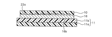
- the method for preparing a chip with a sheet-shaped resin composition is a sheet-shaped resin composition of a bump-forming surface 22a on which a bump 18 of a semiconductor wafer 16 is formed and a tape-integrated sheet-shaped resin composition 100 for back grinding.
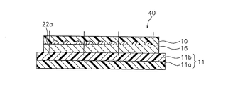
- a bonding process for grinding the back surface 16b of the semiconductor wafer 16 a wafer fixing process for bonding the dicing tape 11 to the back surface 16b of the semiconductor wafer 16 a peeling process for peeling the back surface grinding tape 12, a semiconductor It includes a dicing step of dicing the wafer 16 to form the semiconductor chip 40 with the sheet-shaped resin composition, and a pickup step of peeling the semiconductor chip 40 with the sheet-shaped resin composition from the dicing tape 11.
- a plurality of bumps 18 are formed on the bump forming surface 22a of the semiconductor wafer 16 (see FIG. 2).
- the height of the bump 18 is determined according to the application, and is generally about 5 to 100 ⁇ m. Of course, the height of each bump 18 in the semiconductor wafer 16 may be the same or different.
- the height X ( ⁇ m) of the bump 18 formed on the surface of the semiconductor wafer 16 and the thickness Y ( ⁇ m) of the sheet-shaped resin composition 10 satisfy the relationship of 0.5 ⁇ Y / X ⁇ 2. . More preferably, 0.5 ⁇ Y / X ⁇ 1.5, and still more preferably 0.8 ⁇ Y / X ⁇ 1.3.
- the height X ( ⁇ m) of the bump 18 and the thickness Y ( ⁇ m) of the sheet-shaped resin composition 10 satisfy the above relationship, the space between the semiconductor chip 22 and the mounting substrate 50 is sufficiently filled.
- the sheet-like resin composition 10 can be prevented from excessively protruding from the space, and contamination of the semiconductor chip 22 by the sheet-like resin composition 10 can be prevented.
- the heights of the bumps 18 are different, the height of the highest bump 18 is used as a reference.
- the separator arbitrarily provided on the sheet-shaped resin composition 10 of the tape-integrated sheet-shaped resin composition 100 for back grinding is appropriately peeled to form bumps 18 of the semiconductor wafer 16 as shown in FIG.
- the formed bump forming surface 22a and the sheet-shaped resin composition 10 are opposed to each other, and the sheet-shaped resin composition 10 and the semiconductor wafer 16 are bonded (mounting).
- the method of bonding is not particularly limited, but a method by pressure bonding is preferable.
- the pressure for pressure bonding is preferably 0.1 MPa or more, more preferably 0.2 MPa or more. When the pressure is 0.1 MPa or more, the unevenness of the bump forming surface 22a of the semiconductor wafer 16 can be embedded satisfactorily.
- the upper limit of the pressure for pressure bonding is not particularly limited, but is preferably 1 MPa or less, more preferably 0.5 MPa or less.
- the bonding temperature is preferably 40 ° C. or higher, more preferably 60 ° C. or higher. When the temperature is 40 ° C. or higher, the viscosity of the sheet-shaped resin composition 10 is reduced, and the unevenness of the semiconductor wafer 16 can be filled without a gap. Further, the bonding temperature is preferably 100 ° C. or lower, more preferably 80 ° C. or lower. When the temperature is 100 ° C. or lower, bonding can be performed while suppressing the curing reaction of the sheet-shaped resin composition 10.
- Bonding is preferably performed under reduced pressure, for example, 1000 Pa or less, preferably 500 Pa or less.
- a minimum is not specifically limited, For example, it is 1 Pa or more.
- the surface (that is, the back surface) 16b opposite to the bump forming surface 22a of the semiconductor wafer 16 is ground (see FIG. 3).
- the thin processing machine used for the back surface grinding of the semiconductor wafer 16 is not particularly limited, and examples thereof include a grinding machine (back grinder) and a polishing pad. Further, the back surface grinding may be performed by a chemical method such as etching. The back surface grinding is performed until the semiconductor wafer 16 has a desired thickness (for example, 20 to 700 ⁇ m).
- the dicing tape 11 is attached to the back surface 16b of the semiconductor wafer 16 (see FIG. 4).
- the dicing tape 11 has a structure in which an adhesive layer 11b is laminated on a substrate 11a.
- the base material 11a and the pressure-sensitive adhesive layer 11b can be suitably produced by using the components and the manufacturing methods shown in the paragraphs of the base material 12a and the pressure-sensitive adhesive layer 12b of the back grinding tape 12.
- the pressure sensitive adhesive layer 12b When the back surface grinding tape 12 is peeled off, if the pressure sensitive adhesive layer 12b has radiation curability, the pressure sensitive adhesive layer 12b is irradiated with radiation to harden the pressure sensitive adhesive layer 12b, so that peeling can be easily performed. Can do.
- the radiation dose may be set as appropriate in consideration of the type of radiation used and the degree of curing of the pressure-sensitive adhesive layer.
- ⁇ Dicing process> In the dicing process, as shown in FIG. 6, the semiconductor wafer 40 and the sheet-shaped resin composition 10 are diced to form the diced semiconductor chip 40 with the sheet-shaped resin composition. Dicing is performed according to a conventional method from the bump forming surface 22a on which the sheet-shaped resin composition 10 of the semiconductor wafer 16 is bonded. For example, a cutting method called full cut that cuts up to the dicing tape 11 can be adopted. It does not specifically limit as a dicing apparatus used at this process, A conventionally well-known thing can be used.
- the expansion can be performed using a conventionally known expanding apparatus.
- the semiconductor chip 40 with a sheet-shaped resin composition is peeled from the dicing tape 11 (the semiconductor chip 40 with a sheet-shaped resin composition is picked up).
- the pickup method is not particularly limited, and various conventionally known methods can be employed.
- the adhesive layer 11b of the dicing tape 11 is an ultraviolet curable type
- the pickup is performed after the adhesive layer 11b is irradiated with ultraviolet rays.
- the adhesive force with respect to the semiconductor chip 22 of the adhesive layer 11b falls, and peeling of the semiconductor chip 22 becomes easy.
- Chip 40 with a sheet-shaped resin composition obtained as described above includes a semiconductor chip 22 on which bumps 18 are formed and a sheet-shaped resin composition 10 that is attached to a bump forming surface 22a of semiconductor chip 22. (See FIG. 8).
- the bumps 18 are embedded in the sheet-shaped resin composition 10, and the bump forming surface 22 a of the semiconductor chip 22 is attached to the sheet-shaped resin composition 10.
- the thickness of the semiconductor chip 22 is not particularly limited, but can be set as appropriate within a range of 10 to 1000 ⁇ m, for example.
- the height of the bumps 18 formed on the semiconductor chip 22 is not particularly limited, but can be set as appropriate within a range of 2 to 300 ⁇ m, for example.
- the constituent material of the bump 18 is not particularly limited, but is preferably solder, Sn—Pb, Pb—Sn—Sb, Sn—Sb, Sn—Pb—Bi, Bi—Sn, Sn—Cu.
- Sn-Pb-Cu, Sn-In, Sn-Ag, Sn-Pb-Ag, Pb-Ag, and Sn-Ag-Cu solders are solders.
- those having a melting point within the range of 210 to 230 ° C. can be preferably used, and among the above solders, for example, Sn—Ag system is preferable.
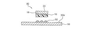
- a mounting substrate 50 having an electrode 52 formed on the surface 50a is prepared (step B).
- the mounting substrate 50 various substrates such as a lead frame and a circuit substrate (such as a wiring circuit substrate) can be used.
- the material of such a substrate is not particularly limited, and examples thereof include a ceramic substrate and a plastic substrate.
- the plastic substrate include an epoxy substrate, a bismaleimide triazine substrate, and a polyimide substrate.
- a semiconductor wafer can be used as the mounting substrate 50.
- Step of making bumps formed on semiconductor chip and electrodes formed on mounting substrate face each other After the step A and the step B, as shown in FIG. 10, a chip 40 with a sheet-like resin composition is attached to a mounting substrate 50 with the sheet-like resin composition 10 as a bonding surface, and a semiconductor.
- the bumps 18 formed on the chip 22 are opposed to the electrodes 52 formed on the mounting substrate 50 (step C).
- the sheet-shaped resin composition 10 of the chip-shaped resin composition-attached chip 40 is arranged to face the mounting substrate 50, and then a flip-chip bonder is used to insert the chip with the sheet-shaped resin composition. Apply pressure from 40 side.
- the temperature at the time of bonding is preferably 100 to 200 ° C., more preferably 150 to 190 ° C. However, the temperature is preferably lower than the melting point of the solder. Further, the pressure at the time of bonding is preferably 0.01 to 10 MPa, more preferably 0.1 to 1 MPa. When the bonding temperature is 150 ° C. or higher, the viscosity of the sheet-shaped resin composition 10 is lowered, and the unevenness can be filled without a gap. Moreover, bonding becomes possible, suppressing the hardening reaction of the sheet-like resin composition 10 as the temperature of bonding is 200 degrees C or less.
- the minimum melt viscosity at less than 200 ° C. of the sheet-shaped resin composition 10 is in the range of 10 Pa ⁇ s to 5000 Pa ⁇ s, the bumps 18 formed on the semiconductor chip 22 and the mounting substrate 50 are formed.
- the electrode 52 can be opposed to the sheet-shaped resin composition 10 while being easily embedded.
- Step D the sheet-shaped resin composition 10 is heated and semi-cured (step D).
- the heating temperature in the step D is preferably 100 to 230 ° C., more preferably 150 to 210 ° C.
- the heating temperature in the step D is preferably lower than the melting point of the solder.
- the heating time is preferably in the range of 1 to 300 seconds, and more preferably in the range of 3 to 120 seconds. At this time, since the thermosetting rate after heating the sheet-shaped resin composition 10 at 200 ° C. for 20 seconds is 50% or more, it is not necessary to raise the temperature greatly after the process C until the semi-curing process of the process D.
- the curing reaction begins and ends early. Since the process D can be completed quickly, the efficiency of the semiconductor device manufacturing process can be improved.
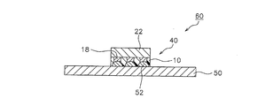
- Step D heating is performed at a higher temperature than the heating in the step D, and as shown in FIG. 11, the bumps 18 and the electrodes 52 are joined, and the sheet-like composition 10 is cured (step E).
- FIG. 11 shows a state in which the bump 18 is made of solder, and the bump 18 and the electrode 52 are joined (electrically connected) by melting the bump 18.
- the heating temperature at this time is preferably 180 to 400 ° C., and more preferably 200 to 300 ° C.
- the heating time is preferably in the range of 1 to 300 seconds, and more preferably in the range of 3 to 120 seconds.
- the bumps 18 are solders having a melting point in the range of 180 to 260 ° C.
- the step D is a step of heating in the range of 100 to 230 ° C.
- the heating in the step D The temperature is preferably lower than the melting point of the solder.
- solder having a melting point in the range of 180 to 260 ° C. is used, the solder is not melted by the heating in the step D.
- the sheet-like resin composition 10 is semi-cured. That is, in the process D, the sheet-shaped resin composition 10 is semi-cured in a mode in which the solder is not melted. In the process D, since solder is not melted, the solder basically does not flow in the process D.
- this process E it heats at a temperature higher than the heating in the said process D, fuses the bump 18 and the electrode 52 by melting the solder, and hardens the sheet-like composition 10.
- the resin constituting the sheet-shaped resin composition 10 is difficult to flow. Therefore, even if the solder is melted for bonding the bump 18 and the electrode 52, the solder is prevented from flowing along with the flow of the sheet-shaped resin composition 10. As a result, it is possible to further suppress occurrence of a short circuit or contact failure due to the solder flow.
- the semiconductor device 60 is obtained.
- the first embodiment has been described above.
- the sheet-shaped resin composition according to the second embodiment is different from the sheet-shaped resin composition 10 according to the first embodiment in that the constituent materials are different, and various physical properties (thermosetting rate, viscosity, viscosity change rate). Etc.). Therefore, in the second embodiment, only differences from the first embodiment will be described, and the description of the other parts will be omitted.
- the sheet-shaped resin composition according to the second embodiment preferably includes an epoxy (meth) acrylate resin and a radical generator.
- Epoxy (meth) acrylate means epoxy acrylate or epoxy methacrylate.
- epoxy (meth) acrylate resin examples include bisphenol A type epoxy (meth) acrylates such as ethoxylated (3) bisphenol A diacrylate.
- the molecular weight (weight average molecular weight) of the epoxy (meth) acrylate resin is not particularly limited, but is preferably 100 to 10,000, and more preferably 200 to 1,000. A weight average molecular weight of 100 to 10000 is preferable in that the cohesive force of the cured product becomes strong.
- the measurement of a weight average molecular weight can be calculated
- the content of the epoxy (meth) acrylate resin with respect to the entire sheet-shaped resin composition is preferably in the range of 2 to 70% by weight from the viewpoint of storage stability and reactivity, and in the range of 10 to 30% by weight. More preferably, it is within.
- the radical generator generates radicals at least by heating.
- radical generators that generate radicals upon heating include organic peroxides and inorganic peroxides such as benzoyl peroxide (BPO), potassium persulfate, and dicumyl peroxide, and azobisisobutyronitrile (AIBN). ) And the like.
- the content of the radical generator with respect to the entire sheet-shaped resin composition is preferably in the range of 0.001 to 2% by weight, and in the range of 0.1 to 1% by weight from the viewpoint of reaction rate. More preferably.
- the sheet-shaped resin composition according to the second embodiment may contain a thermosetting resin. Further, a curing agent may be included.
- the sheet-shaped resin composition includes a thermoplastic resin and the thermoplastic resin has a functional group that undergoes a crosslinking reaction with an epoxy group, it is preferable to include an epoxy resin as a thermosetting resin.
- thermosetting resin examples include epoxy resin, phenol resin, amino resin, unsaturated polyester resin, polyurethane resin, silicone resin, and thermosetting polyimide resin. These resins can be used alone or in combination of two or more. In particular, an epoxy resin containing a small amount of ionic impurities that corrode the semiconductor chip is preferable.
- the epoxy resin is not particularly limited as long as it is generally used as an adhesive composition, for example, bisphenol A type, bisphenol F type, bisphenol S type, brominated bisphenol A type, hydrogenated bisphenol A type, bisphenol AF type.
- a thiol-based curing agent As a curing agent, from the viewpoint of reactivity with thiol-based curing agents and versatility, among the epoxy resins, bisphenol A type, biphenyl type, naphthalene type, phenol novolac type, orthocresol novolak A mold is particularly preferred.
- the content of the thermosetting resin with respect to the entire sheet-shaped resin composition is preferably within the range of 0.1 to 50% by weight, and 0.4 to 20% by weight from the viewpoint of the reliability of the sheet-shaped resin composition. % Is more preferable.
- the sheet-shaped resin composition according to the second embodiment may contain a thermosetting accelerator.
- the thermosetting accelerator is not particularly limited and can be appropriately selected from known thermosetting accelerators.
- a thermosetting accelerator can be used individually or in combination of 2 or more types.
- As the thermosetting accelerator for example, amine-based curing accelerators, phosphorus-based curing accelerators, imidazole-based curing accelerators, boron-based curing accelerators, phosphorus-boron-based curing accelerators, and the like can be used.
- organic compounds containing nitrogen atoms in the molecule for example, amine-based curing accelerators and imidazole-based curing accelerators
- the content of the thermosetting accelerator is preferably in the range of 0.001 to 2% by weight, preferably in the range of 0.01 to 1% by weight, based on 100 parts by weight of the thermosetting resin. More preferred. When it is 0.001 part by weight or more, the thermosetting resin can be sufficiently cured, and when it is 2 part by weight or less, good preservability can be maintained.
- the sheet-shaped resin composition according to the second embodiment preferably contains a thermoplastic resin.
- the thermoplastic resin does not include an epoxy (meth) acrylate resin.
- the thermoplastic resin may contain a carbon-carbon double bond in the molecule.
- thermoplastic resin examples include natural rubber, butyl rubber, isoprene rubber, chloroprene rubber, ethylene-vinyl acetate copolymer, ethylene-acrylic acid copolymer, ethylene-acrylic acid ester copolymer, polybutadiene resin, polycarbonate resin, heat Examples thereof include plastic polyimide resins, polyamide resins such as 6-nylon and 6,6-nylon, phenoxy resins, acrylic resins, saturated polyester resins such as PET and PBT, polyamideimide resins, and fluorine resins. These thermoplastic resins can be used alone or in combination of two or more.
- thermoplastic resins an acrylic resin that has few ionic impurities and high heat resistance and can ensure the reliability of the semiconductor chip is particularly preferable.
- the thermoplastic resin according to the second embodiment has a weight average molecular weight greater than 10,000, and may contain a radical reactive carbon-carbon double bond in the molecule.
- the same acrylic resin as described in the first embodiment can be used within a range not including an epoxy (meth) acrylate resin.
- the content of the thermoplastic resin with respect to the entire sheet-shaped resin composition is preferably 1% by weight or more, more preferably 3% by weight or more. When it is 1% by weight or more, good flexibility is obtained. On the other hand, the content of the thermoplastic resin in the resin component is preferably 40% by weight or less, more preferably 30% by weight or less, and further preferably 25% by weight or less. Good thermal reliability is acquired as it is 40 weight% or less.
- an inorganic filler can be appropriately blended in the sheet-shaped resin composition according to the second embodiment.
- the blending of the inorganic filler makes it possible to improve thermal conductivity, adjust the storage elastic modulus, and the like.
- the inorganic filler those described in the first embodiment can be used, and the blending amount can be the same.
- additives can be appropriately blended with the sheet-shaped resin composition according to the second embodiment as necessary.
- examples of other additives include the same additives as those described in the first embodiment.
- the sheet-shaped resin composition according to the second embodiment can be manufactured by the same method as in the first embodiment. Further, as in the first embodiment, it can be integrated with a back grinding tape. Moreover, it can be used for the manufacturing method of the semiconductor device similar to 1st Embodiment. Therefore, the description here is omitted.
- step A in the present invention is not limited to this example.
- the dicing tape-integrated sheet-shaped resin composition includes a dicing tape and a sheet-shaped resin composition.
- the dicing tape includes a base material and an adhesive layer, and the adhesive layer is provided on the base material.
- the sheet-shaped resin composition is provided on the pressure-sensitive adhesive layer.
- the dicing tape can employ the same configuration as the back grinding tape described above.
- the method for preparing the chip with sheet-shaped resin composition is a method of bonding a bump forming surface on which a bump of a semiconductor wafer is formed and a sheet-shaped resin composition of a dicing tape-integrated sheet-shaped resin composition.
- a method for preparing a chip with a sheet-shaped resin composition using a single sheet-shaped resin composition is, for example, a process of bonding a bump-formed surface on which a bump of a semiconductor wafer is formed and a sheet-shaped resin composition.
- a bonding process a process of bonding a back surface grinding tape to the surface opposite to the semiconductor wafer bonding surface of the sheet-shaped resin composition, a grinding process of grinding the back surface of the semiconductor wafer, and a dicing tape applied to the back surface of the semiconductor wafer Wafer fixing step, peeling step for peeling back surface grinding tape, dicing step for dicing semiconductor wafer to form semiconductor chip with sheet resin composition, and pickup for peeling semiconductor chip with sheet resin composition from dicing tape Process.
- a bump-forming surface on which a bump of a semiconductor wafer is formed a sheet-shaped resin composition
- Bonding process bonding the dicing tape to the surface of the sheet-shaped resin composition opposite to the semiconductor wafer bonding surface, dicing the semiconductor wafer to form a semiconductor chip with the sheet-shaped resin composition
- the sheet-shaped resin composition of the present invention is one that seals the gap between the semiconductor chip and the mounting substrate (so-called underfill sheet) has been described.
- the sheet-shaped resin composition of the present invention is not particularly limited as long as it is used for manufacturing a semiconductor device, that is, for manufacturing a semiconductor device.
- it may be a die bond film for die bonding a semiconductor element to an adherend, or a flip chip type semiconductor back film for forming on the back surface of a semiconductor element flip chip connected on the adherend.
- the sealing film for sealing a semiconductor element may be sufficient.
- Phenol-based curing agent Trade name “MEH-7785H”, manufactured by Meiwa Kasei Co., Ltd. Flux: 2-phenoxybenzoic acid
- Inorganic filler spherical silica (trade name “SO-25R”, manufactured by Admatechs Co., Ltd., average particle diameter: 500nm)
- Thermosetting accelerator Imidazole-based curing accelerator (trade name “2PHZ-PW”, manufactured by Shikoku Kasei Co., Ltd.)
- Radical generator Organic peroxide (trade name “Park Mill D”, manufactured by NOF Corporation)
- Example 2 Comparative Example 1, and Comparative Example 2
- coating on a process film the sheet-like resin composition which concerns on Example 1, Example 2, the comparative example 1, and the comparative example 2 was produced by making it dry at 130 degreeC for 2 minutes.
- all thicknesses were 35 ⁇ m.
- this adhesive composition solution was applied as a release liner (separator) on a release treatment film made of a polyethylene terephthalate film having a thickness of 38 ⁇ m and subjected to silicone release treatment. Then, the sheet-like resin composition which concerns on Example 3 and Example 4 was produced by making it dry at 120 degreeC for 3 minute (s). In Examples 3 and 4, all thicknesses were 35 ⁇ m.
- thermosetting rate after heating at 120 ° C. for 10 minutes was measured as follows. For the measurement, a differential scanning calorimeter manufactured by TA Instruments, product name “Q2000” was used. First, the temperature of the sheet-shaped resin composition that has not been heat-cured is increased from ⁇ 10 ° C. to 350 ° C. (the temperature at which the thermosetting reaction is assumed to be completely completed) at a temperature increase rate of 10 ° C./min. The calorific value (reaction calorie of the uncured sample) was measured. At this time, the exothermic peak temperature was also read. This value is shown in Table 1.
- thermosetting rate [ ⁇ (reaction heat amount of uncured sample) ⁇ (reaction heat amount of sample heated at 120 ° C.
- thermosetting rate after heating at 200 degreeC for 20 seconds was measured as follows.
- a differential scanning calorimeter manufactured by TA Instruments, product name “Q2000” was used.
- the temperature of the sheet-shaped resin composition that has not been heat-cured is increased from ⁇ 10 ° C. to 350 ° C. (the temperature at which the thermosetting reaction is assumed to be completely completed) at a temperature increase rate of 10 ° C./min.
- the calorific value reaction calorie of the uncured sample was measured.
- a sample was prepared by heating the sheet-shaped resin composition at 200 ° C.
- thermosetting rate [ ⁇ (reaction heat amount of uncured sample) ⁇ (reaction heat amount of sample heated at 200 ° C.
- the measured viscosities at 120 ° C. before storage for 1 week and after storage were compared, and the case where the change in viscosity after storage and the viscosity before storage was 1000 Pa ⁇ s or less was evaluated as ⁇ , and the case where it was larger than 1000 Pa ⁇ s was evaluated as x.
- the reason for setting the evaluation criteria as described above is that when the viscosity change is 1000 Pa ⁇ s or less, the bonding at the time of mounting becomes good.
- Table 1 also shows the measured viscosities at 120 ° C. before and after storage.
- [Preservation evaluation 2] Compare the measured viscosities at 120 ° C. before and after storage for 1 week measured in the above storage stability evaluation 1, and the rate of change in viscosity from before storage to after storage (viscosity change rate X1) is in the range of 0 to 20% The case of was evaluated as ⁇ , the case of 20% to 40% as ⁇ , and the case of exceeding 40% as ⁇ . The reason for setting the evaluation criteria as described above is that when the viscosity change rate is 20% or less, the bonding at the time of mounting becomes good. The results are shown in Table 1.
- the viscosity change rate X1 is an absolute value of a value obtained by the following formula.
- the viscosity change rate X2 is an absolute value of a value obtained by the following formula.
- [Viscosity change rate X2 (%)] [100 ⁇ ⁇ (viscosity at 120 ° C. after storage for 2 weeks) ⁇ (viscosity at 120 ° C. before storage) ⁇ / (viscosity at 120 ° C. before storage)
- a mounting substrate (electrode height: 15 ⁇ m) having electrodes was attached to the sample A.
- a flip chip bonder FC3000W manufactured by Toray Engineering Co., Ltd. was used. The pasting conditions were a load: 0.5 Mpa, held at 200 ° C. for 10 seconds, and then held at 260 ° C. for 10 seconds.
- the obtained sample after mounting was polished in parallel with the chip (wafer) to expose the sheet-shaped resin composition.
- the void state of the exposed resin portion was confirmed with an optical microscope (200 times), and when no void (maximum diameter: more than 3 ⁇ m) was confirmed, “ ⁇ ”, the occurrence of a void was confirmed even at one location. Cases were evaluated as “x”.
- Table 1 In the examples, since the sheet-shaped resin composition was sufficiently semi-cured when held at 200 ° C. for 10 seconds, it is considered that expansion of voids was suppressed. On the other hand, in Comparative Example 2, it is considered that the expansion of the void was not suppressed because the sheet-shaped resin composition was not sufficiently cured when held at 200 ° C. for 10 seconds.
Landscapes
- Chemical & Material Sciences (AREA)
- Organic Chemistry (AREA)
- Chemical Kinetics & Catalysis (AREA)
- Medicinal Chemistry (AREA)
- Polymers & Plastics (AREA)
- Health & Medical Sciences (AREA)
- Engineering & Computer Science (AREA)
- Manufacturing & Machinery (AREA)
- Thermal Sciences (AREA)
- Physics & Mathematics (AREA)
- Materials Engineering (AREA)
- Adhesive Tapes (AREA)
- Adhesives Or Adhesive Processes (AREA)
- Mechanical Treatment Of Semiconductor (AREA)
- Structures Or Materials For Encapsulating Or Coating Semiconductor Devices Or Solid State Devices (AREA)
- Wire Bonding (AREA)
Abstract
保存性がよく、且つ、半導体装置の製造プロセスにおいて速硬化性を有するシート状樹脂組成物を提供すること。 120℃で10分加熱した後の熱硬化率が40%以下であり、200℃で20秒加熱した後の熱硬化率が50%以上である半導体装置製造用のシート状樹脂組成物。
Description
本発明は、シート状樹脂組成物、裏面研削用テープ一体型シート状樹脂組成物、及び、半導体装置の製造方法に関する。
従来、半導体チップが基板上にフリップチップボンディングにより実装された(フリップチップ接続された)フリップチップ型の半導体装置に用いられるシート状樹脂組成物であって、半導体チップと基板との間隙の封止用に用いるシート状樹脂組成物が知られている(例えば、特許文献1参照)。
特許文献1のようなシート状樹脂組成物においては、熱硬化性樹脂としてエポキシ樹脂が用いられるとともに、その硬化剤としてフェノール樹脂が用いられることが多い。
しかしながら、エポキシ樹脂の硬化反応において、フェノール樹脂を硬化剤として用いた場合、硬化開始温度から硬化終了温度までの温度幅は、比較的広い。そのため、低温であっても硬化反応が徐々に進行してしまい、シート状樹脂組成物の状態での保存性が乏しくなるといった問題があることを本発明者らは突き止めた。
これを解消する方法としては、保存時に硬化反応が進行しない程度に高温で反応が開始されるようなフェノール樹脂を硬化剤として使用する方法が考えられた。しかしながら、このようなフェノール樹脂を用いると、半導体装置の製造プロセスにおける硬化反応においてより高温、より長時間の加熱が必要となり、製造効率が低下することとなる。
これを解消する方法としては、保存時に硬化反応が進行しない程度に高温で反応が開始されるようなフェノール樹脂を硬化剤として使用する方法が考えられた。しかしながら、このようなフェノール樹脂を用いると、半導体装置の製造プロセスにおける硬化反応においてより高温、より長時間の加熱が必要となり、製造効率が低下することとなる。
本発明は上述した課題に鑑みてなされたものであり、その目的は、保存性がよく、且つ、半導体装置の製造プロセスにおいて速硬化性を有するシート状樹脂組成物を提供することにある。また、当該シート状樹脂組成物を有する裏面研削用テープ一体型シート状樹脂組成物を提供することにある。また、当該シート状樹脂組成物を用いた半導体装置の製造方法を提供することにある。
本願発明者等は、下記の構成を採用することにより、前記の課題を解決できることを見出して本発明を完成させるに至った。
すなわち、本発明は、半導体装置製造用のシート状樹脂組成物であって、
120℃で10分加熱した後の熱硬化率が40%以下であり、
200℃で20秒加熱した後の熱硬化率が50%以上であることを特徴とする。
120℃で10分加熱した後の熱硬化率が40%以下であり、
200℃で20秒加熱した後の熱硬化率が50%以上であることを特徴とする。
本発明に係るシート状樹脂組成物によれば、120℃で10分加熱した後の熱硬化率が40%以下であり、低温における硬化反応の進行が抑制されている。従って、シート状樹脂組成物の状態での保存性に優れる。
また、200℃で20秒加熱した後の熱硬化率が50%以上であるため、半導体装置の製造プロセスにおける硬化反応においてそれほど高温ではない条件、且つ、短時間で硬化反応を進行させることができる。その結果、製造効率を向上させることができる。
このように、本発明に係るシート状樹脂組成物によれば、保存性がよく、且つ、半導体装置の製造プロセスにおいて速硬化性を有するシート状樹脂組成物を提供することができる。
また、200℃で20秒加熱した後の熱硬化率が50%以上であるため、半導体装置の製造プロセスにおける硬化反応においてそれほど高温ではない条件、且つ、短時間で硬化反応を進行させることができる。その結果、製造効率を向上させることができる。
このように、本発明に係るシート状樹脂組成物によれば、保存性がよく、且つ、半導体装置の製造プロセスにおいて速硬化性を有するシート状樹脂組成物を提供することができる。
前記熱硬化率は、加熱前の状態を0%、完全に熱硬化した状態を100%とし、示差走査熱量測定(DSC)により得られる反応熱から求めた値である。より詳しくは後に説明する。
前記構成においては、エポキシ(メタ)アクリレート樹脂と、ラジカル発生剤とを含むことが好ましい。
ラジカル発生剤は、一般的に、ラジカルを発生させる条件にならない限りラジカルをほとんど発生させず、ラジカルを発生させる条件になると、ラジカルを発生させる。エポキシ(メタ)アクリレート樹脂は、炭素-炭素二重結合を有している。本発明では、ラジカル発生剤からラジカルが発生し、エポキシ(メタ)アクリレート樹脂の有する炭素-炭素二重結合が関与するラジカル付加反応が一旦始まると、このラジカル付加反応は連鎖的に進行する。
従って、室温(例えば、120℃以下)ではラジカルを発生させない一方、室温よりは高温であるが比較的低温(例えば、200℃)の条件でラジカルを発生させるようなラジカル発生剤を用いれば、シート状樹脂組成物の120℃で10分加熱した後の熱硬化率を40%以下とし、かつ、200℃での20秒加熱した後の熱硬化率を50%以上とし易くなる。
なお、エポキシ(メタ)アクリレート樹脂は、硬化剤と反応するエポキシ基を有していることを要しない。ただし、例えば、ジグリシジルエーテルと(メタ)アクリル酸とのエステル反応によりエポキシ(メタ)アクリレート樹脂を製造する場合等、エポキシ基はごく少量残る場合はあり得る。つまり、エポキシ(メタ)アクリレート樹脂は、硬化反応として寄与する程度にエポキシ基を有していることを要しない。例えば、オキシラン酸素濃度が0.2%重量以下であればよい。ただし、炭素-炭素二重結合とは別に、官能基としてエポキシ基を有していてもよい。
従って、室温(例えば、120℃以下)ではラジカルを発生させない一方、室温よりは高温であるが比較的低温(例えば、200℃)の条件でラジカルを発生させるようなラジカル発生剤を用いれば、シート状樹脂組成物の120℃で10分加熱した後の熱硬化率を40%以下とし、かつ、200℃での20秒加熱した後の熱硬化率を50%以上とし易くなる。
なお、エポキシ(メタ)アクリレート樹脂は、硬化剤と反応するエポキシ基を有していることを要しない。ただし、例えば、ジグリシジルエーテルと(メタ)アクリル酸とのエステル反応によりエポキシ(メタ)アクリレート樹脂を製造する場合等、エポキシ基はごく少量残る場合はあり得る。つまり、エポキシ(メタ)アクリレート樹脂は、硬化反応として寄与する程度にエポキシ基を有していることを要しない。例えば、オキシラン酸素濃度が0.2%重量以下であればよい。ただし、炭素-炭素二重結合とは別に、官能基としてエポキシ基を有していてもよい。
前記構成においては、熱硬化性樹脂と、硬化剤とを含有し、前記熱硬化性樹脂は、エポキシ樹脂であり、前記硬化剤は、分子内に2つ以上のメルカプト基を有するチオール系硬化剤であることも好ましい。
チオール系硬化剤は、一般的に、フェノール樹脂に比較して、硬化開始温度から硬化終了温度までの温度幅が狭い。従って、エポキシ樹脂の硬化剤としてチオール系硬化剤を用いれば、120℃で10分加熱した後の熱硬化率を40%以下とし、且つ、200℃で20秒加熱した後の熱硬化率が50%以上とし易い。
前記構成においては、熱可塑性樹脂を含有し、前記熱可塑性樹脂は、重量平均分子量が3×10⁵以上のアクリル樹脂であることが好ましい。
熱可塑性樹脂として重量平均分子量が3×10⁵以上のアクリル樹脂を含有すると、樹脂組成物をシート状とし易い。
また、本発明に係る裏面研削用テープ一体型シート状樹脂組成物は、前記シート状樹脂組成物が、裏面研削用テープ上に積層されていることを特徴とする。
本発明に係る裏面研削用テープ一体型シート状樹脂組成物によれば、前記シート状樹脂組成物が、予め裏面研削用テープ上に積層されているため、半導体装置の製造プロセスにおいて、裏面研削用テープをシート状樹脂組成物に貼り合わせる工程等を省略することができる。また、前記シート状樹脂組成物は、120℃で10分加熱した後の熱硬化率が40%以下であり、200℃で20秒加熱した後の熱硬化率が50%以上であるため、保存性がよく、且つ、半導体装置の製造プロセスにおいて速硬化性を有する。
また、本発明に係る半導体装置の製造方法は、
半導体チップのバンプ形成面に、前記シート状樹脂組成物が貼り付けられたシート状樹脂組成物付きチップを準備する工程Aと、
電極が形成された実装用基板を準備する工程Bと、
前記実装用基板に、前記シート状樹脂組成物付きチップを、前記シート状樹脂組成物を貼り合わせ面にして貼り付けて、前記半導体チップに形成された前記バンプと前記実装用基板に形成された電極とを対向させる工程Cと、
前記工程Cの後に、前記シート状樹脂組成物を加熱して半硬化させる工程Dと、
前記工程Dの後に、前記工程Dにおける加熱よりも高温で加熱し、前記バンプと前記電極とを接合するとともに、前記シート状組成物を硬化させる工程Eとを含むことを特徴とする。
半導体チップのバンプ形成面に、前記シート状樹脂組成物が貼り付けられたシート状樹脂組成物付きチップを準備する工程Aと、
電極が形成された実装用基板を準備する工程Bと、
前記実装用基板に、前記シート状樹脂組成物付きチップを、前記シート状樹脂組成物を貼り合わせ面にして貼り付けて、前記半導体チップに形成された前記バンプと前記実装用基板に形成された電極とを対向させる工程Cと、
前記工程Cの後に、前記シート状樹脂組成物を加熱して半硬化させる工程Dと、
前記工程Dの後に、前記工程Dにおける加熱よりも高温で加熱し、前記バンプと前記電極とを接合するとともに、前記シート状組成物を硬化させる工程Eとを含むことを特徴とする。
本発明に係る半導体装置の製造方法によれば、120℃で10分加熱した後の熱硬化率が40%以下であり、200℃で20秒加熱した後の熱硬化率が50%以上であるシート状樹脂組成物を用いているため、工程Cの後、工程Dの半硬化工程までに大きく温度を上げなくても、硬化反応が始まり早期に終了する。工程Dを速やかに終了させることができるため、半導体装置の製造プロセスの効率化が図れる。
本発明によれば、保存性がよく、且つ、半導体装置の製造プロセスにおいて速硬化性を有するシート状樹脂組成物を提供することができる。また、当該シート状樹脂組成物を有する裏面研削用テープ一体型シート状樹脂組成物を提供することができる。また、当該シート状樹脂組成物を用いた半導体装置の製造方法を提供することができる。
以下、本発明の実施形態について、図面を参照しつつ説明する。
[第1実施形態]
まず、第1実施形態について説明する。
まず、第1実施形態について説明する。
[裏面研削用テープ一体型シート状樹脂組成物]
図1は、本発明の一実施形態に係る裏面研削用テープ一体型シート状樹脂組成物を示す断面模式図である。図1に示すように、本実施形態に係る裏面研削用テープ一体型シート状樹脂組成物100は、裏面研削用テープ12と、裏面研削用テープ12上に積層されたシート状樹脂組成物10とを備える。裏面研削用テープ12は、基材12a及び粘着剤層12bを備え、粘着剤層12bは基材12a上に設けられている。シート状樹脂組成物10は粘着剤層12b上に設けられている。なお、シート状樹脂組成物10は、図1に示したように裏面研削用テープ12の全面に積層されていなくてもよく、半導体ウェハ16(図2参照)との貼り合わせに十分なサイズで設けられていればよい。
図1は、本発明の一実施形態に係る裏面研削用テープ一体型シート状樹脂組成物を示す断面模式図である。図1に示すように、本実施形態に係る裏面研削用テープ一体型シート状樹脂組成物100は、裏面研削用テープ12と、裏面研削用テープ12上に積層されたシート状樹脂組成物10とを備える。裏面研削用テープ12は、基材12a及び粘着剤層12bを備え、粘着剤層12bは基材12a上に設けられている。シート状樹脂組成物10は粘着剤層12b上に設けられている。なお、シート状樹脂組成物10は、図1に示したように裏面研削用テープ12の全面に積層されていなくてもよく、半導体ウェハ16(図2参照)との貼り合わせに十分なサイズで設けられていればよい。
(シート状樹脂組成物)
シート状樹脂組成物10は、半導体チップ22を実装用基板50(図9参照)に実装する際に、半導体チップ22と実装用基板50との間隙を封止する機能を有する。
シート状樹脂組成物10は、半導体チップ22を実装用基板50(図9参照)に実装する際に、半導体チップ22と実装用基板50との間隙を封止する機能を有する。
シート状樹脂組成物10は、120℃で10分加熱した後の熱硬化率が40%以下であり、35%以下であることが好ましく、30%以下であることがより好ましい。シート状樹脂組成物10は、120℃で10分加熱した後の熱硬化率が40%以下であり、低温における硬化反応の進行が抑制されている。従って、シート状樹脂組成物の状態での保存性に優れる。
また、シート状樹脂組成物10は、200℃で20秒加熱した後の熱硬化率が50%以上であり、60%以上であることが好ましく、70%以上であることがより好ましい。シート状樹脂組成物10は、200℃で20秒加熱した後の熱硬化率が50%以上であるため、半導体装置の製造プロセスにおける硬化反応においてそれほど高温ではない条件、且つ、短時間で硬化反応を進行させることができる。その結果、製造効率を向上させることができる。
このように、シート状樹脂組成物10によれば、保存性がよく、且つ、半導体装置の製造プロセスにおいて速硬化性を有するシート状樹脂組成物を提供することができる。
シート状樹脂組成物10の120℃で10分加熱した後の熱硬化率、及び、200℃で20秒加熱した後の熱硬化率は、シート状樹脂組成物10に含有する硬化剤の種類や、硬化促進剤の種類、硬化促進剤の含有量、各種の添加剤等によりコントロールすることができる。
また、シート状樹脂組成物10は、200℃で20秒加熱した後の熱硬化率が50%以上であり、60%以上であることが好ましく、70%以上であることがより好ましい。シート状樹脂組成物10は、200℃で20秒加熱した後の熱硬化率が50%以上であるため、半導体装置の製造プロセスにおける硬化反応においてそれほど高温ではない条件、且つ、短時間で硬化反応を進行させることができる。その結果、製造効率を向上させることができる。
このように、シート状樹脂組成物10によれば、保存性がよく、且つ、半導体装置の製造プロセスにおいて速硬化性を有するシート状樹脂組成物を提供することができる。
シート状樹脂組成物10の120℃で10分加熱した後の熱硬化率、及び、200℃で20秒加熱した後の熱硬化率は、シート状樹脂組成物10に含有する硬化剤の種類や、硬化促進剤の種類、硬化促進剤の含有量、各種の添加剤等によりコントロールすることができる。
前記熱硬化率は、示差走査熱量測定(DSC)を用い、発熱量を測定して求める。具体的には、まず、熱硬化させていないシート状樹脂組成物を作成し、-10℃から昇温速度10℃/分の条件で、350℃(熱硬化反応が完全に完了したと想定される温度)まで昇温した際の発熱量(未硬化サンプルの反応熱量)を測定する。また、熱硬化前のシート状樹脂組成物を、所定条件(120℃で10分加熱、又は、200℃で20秒加熱)で加熱したサンプルを作成する。
次に、所定条件で加熱したサンプルについて、-10℃から昇温速度10℃/分の条件で、350℃(熱硬化反応が完全に完了したと想定される温度)まで昇温した際の発熱量(所定条件で熱硬化させたサンプルの反応熱量)を測定する。その後、以下の式(1)により熱硬化率を得る。なお、発熱量は、示差走査熱量計にて測定される発熱ピークの立ち上がり温度と反応終了温度の2点を結んだ直線とピークで囲まれる面積を用いて求める。
次に、所定条件で加熱したサンプルについて、-10℃から昇温速度10℃/分の条件で、350℃(熱硬化反応が完全に完了したと想定される温度)まで昇温した際の発熱量(所定条件で熱硬化させたサンプルの反応熱量)を測定する。その後、以下の式(1)により熱硬化率を得る。なお、発熱量は、示差走査熱量計にて測定される発熱ピークの立ち上がり温度と反応終了温度の2点を結んだ直線とピークで囲まれる面積を用いて求める。
式(1):
熱硬化率=[{(未硬化サンプルの反応熱量)-(所定条件で熱硬化させたサンプルの反応熱量)}/(未硬化サンプルの反応熱量)]×100(%)
熱硬化率=[{(未硬化サンプルの反応熱量)-(所定条件で熱硬化させたサンプルの反応熱量)}/(未硬化サンプルの反応熱量)]×100(%)
シート状樹脂組成物10は、示差走査熱量測定において10℃/minの昇温条件で測定した際に、熱硬化のピーク温度が130℃~190℃の範囲内となるように調製されたものが好ましい。前記熱硬化のピーク温度を130℃~190℃の範囲内となるように調整する方法としては、例えば、硬化促進剤の種類、硬化促進剤の含有量により調整する方法を挙げることができる。
シート状樹脂組成物10は、120℃における粘度が0.1kPa・s以上10kPa・s以下であることが好ましく、0.5kPa・s以上9kPa・s以下であることがより好ましく、1kPa・s以上8kPa・s以下であることがさらに好ましい。シート状樹脂組成物10の120℃における粘度が0.1kPa・s以上であると、工程Cの温度から半硬化工程Dの温度に昇温する際のボイド膨張を抑制することができる。一方、10kPa・s以下であると、実装用基板の凹凸へシート状樹脂組成物を埋め込むことができる。
シート状樹脂組成物10は、温度:25℃の条件で、1週間保存した後の120℃での粘度と、保存前における120℃での粘度との粘度変化率X1が、絶対値で0~40%の範囲内であることが好ましく、0~20%の範囲内であることがより好ましい。なお、粘度変化率X1は、下記式により得られる値である。
[粘度変化率X1(%)]=[100×{(1週間保存後の120℃での粘度)-(保存前の120℃での粘度)}/(保存前の120℃での粘度)]
[粘度変化率X1(%)]=[100×{(1週間保存後の120℃での粘度)-(保存前の120℃での粘度)}/(保存前の120℃での粘度)]
シート状樹脂組成物10は、温度:25℃の条件で、2週間保存した後の120℃での粘度と、保存前における120℃での粘度との粘度変化率X2が、絶対値で0~40%の範囲内であることが好ましく、0~20%の範囲内であることがより好ましい。なお、粘度変化率X2は、下記式により得られる値である。
[粘度変化率X2(%)]=[100×{(2週間保存後の120℃での粘度)-(保存前の120℃での粘度)}/(保存前の120℃での粘度)]
[粘度変化率X2(%)]=[100×{(2週間保存後の120℃での粘度)-(保存前の120℃での粘度)}/(保存前の120℃での粘度)]
シート状樹脂組成物10は200℃未満における最低溶融粘度が10Pa・s~5000Pa・sの範囲内にあることが好ましく、50Pa・s~3000Pa・sの範囲内にあることがより好ましく、100Pa・s~2000Pa・sの範囲内にあることがさらに好ましい。シート状樹脂組成物10の200℃未満における最低溶融粘度が10Pa・s~5000Pa・sの範囲内にあると、後述する工程Cにおいて、半導体チップ22に形成されたバンプ18と実装用基板50に形成された電極52とを容易にシート状樹脂組成物10に埋め込みながら、対向させることができる。
シート状樹脂組成物10の200℃未満における最低溶融粘度とは、熱硬化前の200℃未満における最低溶融粘度をいう。
シート状樹脂組成物10の200℃未満における最低溶融粘度は、シート状樹脂組成物10の構成材料の選択によりコントロールすることができる。特に、熱可塑性樹脂の選択によりコントロールすることができる。具体的に、熱可塑性樹脂として、例えば、低分子量のものを使用すると、200℃未満における最低溶融粘度を小さくすることができ、例えば、高分子量のものを使用すると、200℃未満における最低溶融粘度を大きくすることができる。
シート状樹脂組成物10は、熱硬化性樹脂を含むことが好ましい。また、シート状樹脂組成物10は、硬化剤を含むことが好ましい。
前記熱硬化性樹脂としては、エポキシ樹脂、フェノール樹脂、アミノ樹脂、不飽和ポリエステル樹脂、ポリウレタン樹脂、シリコーン樹脂、又は熱硬化性ポリイミド樹脂等が挙げられる。これらの樹脂は、単独で又は2種以上を併用して用いることができる。特に、半導体チップを腐食させるイオン性不純物等の含有が少ないエポキシ樹脂が好ましい。
前記エポキシ樹脂は、接着剤組成物として一般に用いられるものであれば特に限定は無く、例えばビスフェノールA型、ビスフェノールF型、ビスフェノールS型、臭素化ビスフェノールA型、水添ビスフェノールA型、ビスフェノールAF型、ビフェニル型、ナフタレン型、フルオンレン型、フェノールノボラック型、オルソクレゾールノボラック型、トリスヒドロキシフェニルメタン型、テトラフェニロールエタン型等の二官能エポキシ樹脂や多官能エポキシ樹脂、又はヒダントイン型、トリスグリシジルイソシアヌレート型若しくはグリシジルアミン型等のエポキシ樹脂が用いられる。これらは単独で、又は2種以上を併用して用いることができる。硬化剤としてチオール系硬化剤を用いる場合、チオール系硬化剤との反応性や汎用性の観点から、前記エポキシ樹脂のなかでも、ビスフェノールA型、ビフェニル型、ナフタレン型、フェノールノボラック型、オルソクレゾールノボラック型が特に好ましい。
シート状樹脂組成物10全体に対する熱硬化性樹脂の含有量は、シート状樹脂組成物が熱硬化性のシートとしての機能を発揮できる程度であれば特に限定されず、5~50重量%の範囲内であることが好ましく、10~30重量%の範囲内であることがより好ましい。
前記硬化剤は、熱硬化性樹脂の種類に応じて、適宜選択することができる。前記熱硬化性樹脂がエポキシ樹脂である場合、前記硬化剤としては、分子内に2つ以上のメルカプト基を有するチオール系硬化剤が好ましい。なかでも、分子内に4つのメルカプト基を有するチオール系硬化剤が好ましい。チオール系硬化剤は、一般的に、フェノール樹脂に比較して、硬化開始温度から硬化終了温度までの温度幅が狭い。従って、エポキシ樹脂の硬化剤としてチオール系硬化剤を用いれば、120℃で10分加熱した後の熱硬化率を40%以下とし、且つ、200℃で20秒加熱した後の熱硬化率が50%以上とし易い。
前記チオール系硬化剤のなかでも、分子内に1つ以上の第2級メルカプト基を有するチオール系硬化剤がより好ましく、分子内に4つの第2級メルカプト基を有するチオール系硬化剤がさらに好ましい。一般に、第2級メルカプト基は、メチル基の存在による立体障害が大きく、第1級メルカプト基に比べてエポキシ基との反応性が低い。また、第2級メルカプト基は、β位のカルボニル基に内部水素結合することができるため、安定な状態となり反応性が低下する。そのため、シート状樹脂組成物10の120℃で10分加熱した後の熱硬化率をより40%以下とし易い。
チオール系硬化剤のなかでも、シート状樹脂組成物10の硬化開始温度をフェノール樹脂を用いた場合よりも高くする(例えば、120~180℃程度)ことができるものが好ましい。このようなチオール系硬化剤の具体例としては、分子内に第2級メルカプト基を有する下記式(2)で示されるペンタエリスリトールテトラキス(3-メルカプトブチレート)、下記式(3)で示される1,4-ビス(3-メルカプトブチリルオキシ)ブタン、下記式(4)で示される1,3,5-トリス(3-メルカプトブチリルオキシエチル)1,3,5-トリアジン-2,4,6(1H,3H,5H)-トリオン等が挙げられる。
前記チオール系硬化剤のなかでも、分子内に1つ以上の第2級メルカプト基を有するチオール系硬化剤がより好ましく、分子内に4つの第2級メルカプト基を有するチオール系硬化剤がさらに好ましい。一般に、第2級メルカプト基は、メチル基の存在による立体障害が大きく、第1級メルカプト基に比べてエポキシ基との反応性が低い。また、第2級メルカプト基は、β位のカルボニル基に内部水素結合することができるため、安定な状態となり反応性が低下する。そのため、シート状樹脂組成物10の120℃で10分加熱した後の熱硬化率をより40%以下とし易い。
チオール系硬化剤のなかでも、シート状樹脂組成物10の硬化開始温度をフェノール樹脂を用いた場合よりも高くする(例えば、120~180℃程度)ことができるものが好ましい。このようなチオール系硬化剤の具体例としては、分子内に第2級メルカプト基を有する下記式(2)で示されるペンタエリスリトールテトラキス(3-メルカプトブチレート)、下記式(3)で示される1,4-ビス(3-メルカプトブチリルオキシ)ブタン、下記式(4)で示される1,3,5-トリス(3-メルカプトブチリルオキシエチル)1,3,5-トリアジン-2,4,6(1H,3H,5H)-トリオン等が挙げられる。

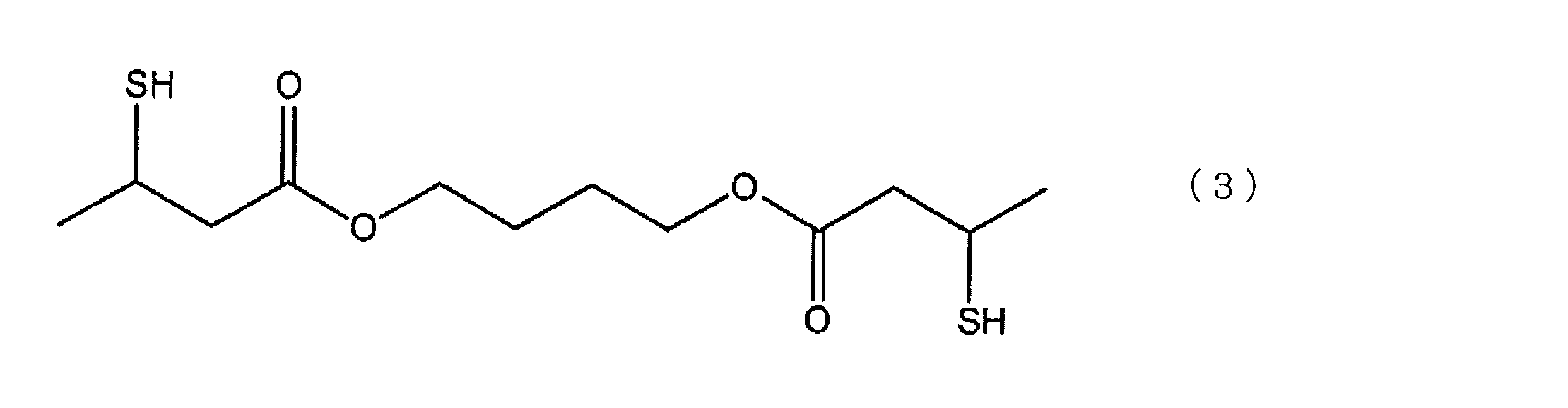

前記熱硬化性樹脂がエポキシ樹脂である場合、前記硬化剤の配合量としては、特に限定されないが、シート状樹脂組成物10全体に対して5~30重量%が好ましく、10~20重量%がより好ましい。
シート状樹脂組成物10は、熱硬化促進剤を含有していてもよい。前記熱硬化促進剤としては、特に制限されず、公知の熱硬化促進剤の中から適宜選択して用いることができる。熱硬化促進剤は単独で又は2種以上を組み合わせて用いることができる。熱硬化促進剤としては、例えば、アミン系硬化促進剤、リン系硬化促進剤、イミダゾール系硬化促進剤、ホウ素系硬化促進剤、リン-ホウ素系硬化促進剤などを用いることができる。なかでも、反応性、溶解性の観点から、窒素原子を分子内に含む有機化合物(例えば、アミン系硬化促進剤、イミダゾール系硬化促進剤)が好ましい。
前記熱硬化促進剤の含有量は、熱硬化性樹脂100重量部に対して、0.3重量部以上であることが好ましく、1.0重量部以上であることがより好ましく、2.0重量部以上であることがさらに好ましい。4.8重量部以上であると、後述する半硬化工程(工程D)において容易にシート状樹脂組成物10を半硬化させることができる。また、熱硬化促進剤の含有量は、好ましくは24重量部以下である。24重量部以下であると、熱硬化性樹脂の保存性を向上させることができる。
シート状樹脂組成物10は、熱可塑性樹脂を含むことが好ましい。前記熱可塑性樹脂としては、天然ゴム、ブチルゴム、イソプレンゴム、クロロプレンゴム、エチレン-酢酸ビニル共重合体、エチレン-アクリル酸共重合体、エチレン-アクリル酸エステル共重合体、ポリブタジエン樹脂、ポリカーボネート樹脂、熱可塑性ポリイミド樹脂、6-ナイロンや6,6-ナイロン等のポリアミド樹脂、フェノキシ樹脂、アクリル樹脂、PETやPBT等の飽和ポリエステル樹脂、ポリアミドイミド樹脂、フッ素樹脂等が挙げられる。これらの熱可塑性樹脂は単独で、又は2種以上を併用して用いることができる。これらの熱可塑性樹脂のうち、イオン性不純物が少なく耐熱性が高く、半導体チップの信頼性を確保できるアクリル樹脂が特に好ましい。
前記アクリル樹脂としては、特に限定されるものではなく、炭素数30以下、特に炭素数4~18の直鎖若しくは分岐のアルキル基を有するアクリル酸又はメタクリル酸のエステルの1種又は2種以上を成分とする重合体等が挙げられる。前記アルキル基としては、例えばメチル基、エチル基、プロピル基、イソプロピル基、n-ブチル基、t-ブチル基、イソブチル基、アミル基、イソアミル基、へキシル基、へプチル基、シクロヘキシル基、2-エチルヘキシル基、オクチル基、イソオクチル基、ノニル基、イソノニル基、デシル基、イソデシル基、ウンデシル基、ラウリル基、トリデシル基、テトラデシル基、ステアリル基、オクタデシル基、又はドデシル基等が挙げられる。
また、前記重合体を形成する他のモノマーとしては、特に限定されるものではなく、例えばアクリル酸、メタクリル酸、カルボキシエチルアクリレート、カルボキシペンチルアクリレート、イタコン酸、マレイン酸、フマール酸若しくはクロトン酸等の様なカルボキシル基含有モノマー、無水マレイン酸若しくは無水イタコン酸等の様な酸無水物モノマー、(メタ)アクリル酸2-ヒドロキシエチル、(メタ)アクリル酸2-ヒドロキシプロピル、(メタ)アクリル酸4-ヒドロキシブチル、(メタ)アクリル酸6-ヒドロキシヘキシル、(メタ)アクリル酸8-ヒドロキシオクチル、(メタ)アクリル酸10-ヒドロキシデシル、(メタ)アクリル酸12-ヒドロキシラウリル若しくは(4-ヒドロキシメチルシクロヘキシル)-メチルアクリレート等の様なヒドロキシル基含有モノマー、スチレンスルホン酸、アリルスルホン酸、2-(メタ)アクリルアミド-2-メチルプロパンスルホン酸、(メタ)アクリルアミドプロパンスルホン酸、スルホプロピル(メタ)アクリレート若しくは(メタ)アクリロイルオキシナフタレンスルホン酸等の様なスルホン酸基含有モノマー、又は2-ヒドロキシエチルアクリロイルホスフェート等の様な燐酸基含有モノマーが挙げられる。
前記アクリル樹脂は、製膜性の観点から、重量平均分子量が3×10⁵以上であることが好ましく、4×10⁵以上であることがより好ましい。前記熱可塑性樹脂として重量平均分子量が3×10⁵以上のアクリル樹脂を含有すると、樹脂組成物をシート状とし易い。重量平均分子量の測定は、GPC(ゲル・パーミエーション・クロマトグラフィー)により行い、ポリスチレン換算により算出した値である。
シート状樹脂組成物10全体に対する熱可塑性樹脂の含有量は、好ましくは1重量%以上であり、より好ましくは3重量%以上である。1重量%以上であると、良好な可とう性が得られる。一方、樹脂成分中の熱可塑性樹脂の含有量は、好ましくは15重量%以下であり、より好ましくは12重量%以下であり、さらに好ましくは8重量%以下である。15重量%以下であると、良好な熱的信頼性が得られる。
また、シート状樹脂組成物10には、無機充填剤を適宜配合することができる。無機充填剤の配合は、熱伝導性の向上、貯蔵弾性率の調節等を可能にする。
前記無機充填剤としては、例えば、シリカ、クレー、石膏、炭酸カルシウム、硫酸バリウム、酸化アルミナ、酸化ベリリウム、炭化珪素、窒化珪素等のセラミック類、カーボン等の無機粉末が挙げられる。これらは、単独で又は2種以上を併用して用いることができる。なかでも、シリカ、特に溶融シリカが好適に用いられる。
無機充填剤の平均粒径は、10~1000nmの範囲内であることが好ましく、20~500nmの範囲内であることがより好ましく、50~300nmの範囲内であることがさらに好ましい。なお、本発明においては、平均粒径が相互に異なる無機充填剤同士を組み合わせ、全体として平均粒径が上記数値範囲内となるようにしてもよい。前記無機充填剤の平均粒径が10nm以上であると、容易に製膜することができる。一方、前記無機充填剤の平均粒径が10000nm以下であると、フィルムに透明性を付与することができる。前記平均粒径は、光度式の粒度分布計(HORIBA製、装置名;LA-910)により求めた値である。
前記無機充填剤の配合量は、有機樹脂成分100重量部に対し50~1400重量部に設定することが好ましい。特に好ましくは100~900重量部である。無機充填剤の配合量を50重量部以上にすると、耐熱性や強度が向上する。また、1400重量部以下とすることにより、流動性が確保できる。これにより、接着性や埋め込み性が低下することを防止できる。
なお、シート状樹脂組成物10には、前記無機充填剤以外に、必要に応じて他の添加剤を適宜に配合することができる。他の添加剤としては、例えば難燃剤、シランカップリング剤、イオントラップ剤、カーボンブラック等の顔料等が挙げられる。前記難燃剤としては、例えば、三酸化アンチモン、五酸化アンチモン、臭素化エポキシ樹脂等が挙げられる。これらは、単独で、又は2種以上を併用して用いることができる。前記シランカップリング剤としては、例えば、β-(3、4-エポキシシクロヘキシル)エチルトリメトキシシラン、γ-グリシドキシプロピルトリメトキシシラン、γ-グリシドキシプロピルメチルジエトキシシラン等が挙げられる。これらの化合物は、単独で又は2種以上を併用して用いることができる。前記イオントラップ剤としては、例えばハイドロタルサイト類、水酸化ビスマス等が挙げられる。これらは、単独で又は2種以上を併用して用いることができる。また、実装時に半田の酸化膜を除去することを目的として、有機酸等のフラックスを添加することもできる。
シート状樹脂組成物10の厚さ(複層の場合は、総厚)は特に限定されないものの、硬化後の樹脂の強度や充填性を考慮すると5μm以上500μm以下が好ましい。なお、シート状樹脂組成物10の厚さは、チップ22と実装用基板50との間隙の幅を考慮して適宜設定することができる。
シート状樹脂組成物10は、例えば、次の通りにして作製される。まず、シート状樹脂組成物10の形成材料である樹脂組成物溶液を作製する。当該樹脂組成物溶液には、前述の通り、前記樹脂組成物やフィラー、その他各種の添加剤等が配合されている。
次に、樹脂組成物溶液を基材セパレータ上に所定厚みとなる様に塗布して塗布膜を形成した後、該塗布膜を所定条件下で乾燥させ、シート状樹脂組成物10を形成する。塗布方法としては特に限定されず、例えば、ロール塗工、スクリーン塗工、グラビア塗工等が挙げられる。また、乾燥条件としては、例えば乾燥温度70~160℃、乾燥時間1~5分間の範囲内で行われる。
(裏面研削用テープ)
裏面研削用テープ12は、基材12aと、基材12a上に積層された粘着剤層12bとを備えている。
裏面研削用テープ12は、基材12aと、基材12a上に積層された粘着剤層12bとを備えている。
上記基材12aは裏面研削用テープ一体型シート状樹脂組成物100の強度母体となるものである。例えば、低密度ポリエチレン、直鎖状ポリエチレン、中密度ポリエチレン、高密度ポリエチレン、超低密度ポリエチレン、ランダム共重合ポリプロピレン、ブロック共重合ポリプロピレン、ホモポリプロレン、ポリブテン、ポリメチルペンテンなどのポリオレフィン、エチレン-酢酸ビニル共重合体、アイオノマー樹脂、エチレン-(メタ)アクリル酸共重合体、エチレン-(メタ)アクリル酸エステル(ランダム、交互)共重合体、エチレン-ブテン共重合体、エチレン-ヘキセン共重合体、ポリウレタン、ポリエチレンテレフタレート、ポリエチレンナフタレートなどのポリエステル、ポリカーボネート、ポリイミド、ポリエーテルエーテルケトン、ポリイミド、ポリエーテルイミド、ポリアミド、全芳香族ポリアミド、ポリフェニルスルフイド、アラミド(紙)、ガラス、ガラスクロス、フッ素樹脂、ポリ塩化ビニル、ポリ塩化ビニリデン、セルロース系樹脂、シリコーン樹脂、金属(箔)、紙などが挙げられる。粘着剤層12bが紫外線硬化型である場合、基材12aは紫外線に対し透過性を有するものが好ましい。
上記基材12aは、同種又は異種のものを適宜に選択して使用することができ、必要に応じて数種をブレンドしたものを用いることができる。基材12aの表面には、慣用の表面処理を施すことができる。基材12aには、帯電防止能を付与するため、上記の基材12a上に金属、合金、これらの酸化物などからなる厚さが30~500Å程度の導電性物質の蒸着層を設けることができる。基材12aは単層又は2種以上の複層でもよい。
基材12aの厚さは適宜に決定でき、一般的には5μm以上200μm以下程度であり、好ましくは35μm以上120μm以下である。
なお、基材12aには、各種添加剤(例えば、着色剤、充填剤、可塑剤、老化防止剤、酸化防止剤、界面活性剤、難燃剤など)が含まれていてもよい。
粘着剤層12bの形成に用いる粘着剤は、半導体ウェハの裏面研削時に半導体ウェハを保持でき、裏面研削後に半導体ウェハから剥離できるものであれば特に制限されない。例えば、アクリル系粘着剤、ゴム系粘着剤などの一般的な感圧性接着剤を用いることができる。上記感圧性接着剤としては、半導体ウェハやガラスなどの汚染をきらう電子部品の超純水やアルコールなどの有機溶剤による清浄洗浄性などの点から、アクリル系ポリマーをベースポリマーとするアクリル系粘着剤が好ましい。
上記アクリル系ポリマーとしては、アクリル酸エステルを主モノマー成分として用いたものが挙げられる。上記アクリル酸エステルとしては、例えば、(メタ)アクリル酸アルキルエステル(例えば、メチルエステル、エチルエステル、プロピルエステル、イソプロピルエステル、ブチルエステル、イソブチルエステル、s-ブチルエステル、t-ブチルエステル、ペンチルエステル、イソペンチルエステル、ヘキシルエステル、ヘプチルエステル、オクチルエステル、2-エチルヘキシルエステル、イソオクチルエステル、ノニルエステル、デシルエステル、イソデシルエステル、ウンデシルエステル、ドデシルエステル、トリデシルエステル、テトラデシルエステル、ヘキサデシルエステル、オクタデシルエステル、エイコシルエステルなどのアルキル基の炭素数1~30、特に炭素数4~18の直鎖状又は分岐鎖状のアルキルエステルなど)及び(メタ)アクリル酸シクロアルキルエステル(例えば、シクロペンチルエステル、シクロヘキシルエステルなど)の1種又は2種以上を単量体成分として用いたアクリル系ポリマーなどが挙げられる。なお、(メタ)アクリル酸エステルとはアクリル酸エステル及び/又はメタクリル酸エステルをいい、本発明の(メタ)とは全て同様の意味である。
上記アクリル系ポリマーは、凝集力、耐熱性などの改質を目的として、必要に応じ、上記(メタ)アクリル酸アルキルエステル又はシクロアルキルエステルと共重合可能な他のモノマー成分に対応する単位を含んでいてもよい。このようなモノマー成分として、例えば、アクリル酸、メタクリル酸、カルボキシエチル(メタ)アクリレート、カルボキシペンチル(メタ)アクリレート、イタコン酸、マレイン酸、フマル酸、クロトン酸などのカルボキシル基含有モノマー;無水マレイン酸、無水イタコン酸などの酸無水物モノマー;(メタ)アクリル酸2-ヒドロキシエチル、(メタ)アクリル酸2-ヒドロキシプロピル、(メタ)アクリル酸4-ヒドロキシブチル、(メタ)アクリル酸6-ヒドロキシヘキシル、(メタ)アクリル酸8-ヒドロキシオクチル、(メタ)アクリル酸10-ヒドロキシデシル、(メタ)アクリル酸12-ヒドロキシラウリル、(4-ヒドロキシメチルシクロヘキシル)メチル(メタ)アクリレートなどのヒドロキシル基含有モノマー;スチレンスルホン酸、アリルスルホン酸、2-(メタ)アクリルアミド-2-メチルプロパンスルホン酸、(メタ)アクリルアミドプロパンスルホン酸、スルホプロピル(メタ)アクリレート、(メタ)アクリロイルオキシナフタレンスルホン酸などのスルホン酸基含有モノマー;2-ヒドロキシエチルアクリロイルホスフェートなどのリン酸基含有モノマー;アクリルアミド、アクリロニトリルなどがあげられる。これら共重合可能なモノマー成分は、1種又は2種以上使用できる。これら共重合可能なモノマーの使用量は、全モノマー成分の40重量%以下が好ましい。
さらに、上記アクリル系ポリマーは、架橋させるため、多官能性モノマーなども、必要に応じて共重合用モノマー成分として含むことができる。このような多官能性モノマーとして、例えば、ヘキサンジオールジ(メタ)アクリレート、(ポリ)エチレングリコールジ(メタ)アクリレート、(ポリ)プロピレングリコールジ(メタ)アクリレート、ネオペンチルグリコールジ(メタ)アクリレート、ペンタエリスリトールジ(メタ)アクリレート、トリメチロールプロパントリ(メタ)アクリレート、ペンタエリスリトールトリ(メタ)アクリレート、ジペンタエリスリトールヘキサ(メタ)アクリレート、エポキシ(メタ)アクリレート、ポリエステル(メタ)アクリレート、ウレタン(メタ)アクリレートなどがあげられる。これらの多官能性モノマーも1種又は2種以上用いることができる。多官能性モノマーの使用量は、粘着特性などの点から、全モノマー成分の30重量%以下が好ましい。
上記アクリル系ポリマーは、単一モノマー又は2種以上のモノマー混合物を重合に付すことにより得られる。重合は、溶液重合、乳化重合、塊状重合、懸濁重合などの何れの方式で行うこともできる。清浄な被着体への汚染防止などの点から、低分子量物質の含有量が小さいのが好ましい。この点から、アクリル系ポリマーの数平均分子量は、好ましくは30万以上、さらに好ましくは40万~300万程度である。
また、上記粘着剤には、ベースポリマーであるアクリル系ポリマーなどの数平均分子量を高めるため、外部架橋剤を適宜に採用することもできる。外部架橋方法の具体的手段としては、ポリイソシアネート化合物、エポキシ化合物、アジリジン化合物、メラミン系架橋剤などのいわゆる架橋剤を添加し反応させる方法があげられる。外部架橋剤を使用する場合、その使用量は、架橋すべきベースポリマーとのバランスにより、さらには、粘着剤としての使用用途によって適宜決定される。一般的には、上記ベースポリマー100重量部に対して、5重量部程度以下、さらには0.1~5重量部配合するのが好ましい。さらに、粘着剤には、必要により、上記成分のほかに、従来公知の各種の粘着付与剤、老化防止剤などの添加剤を用いてもよい。
粘着剤層12bは放射線硬化型粘着剤により形成することができる。放射線硬化型粘着剤は、紫外線などの放射線の照射により架橋度を増大させてその粘着力を容易に低下させることができ、ピックアップを容易に行うことができる。放射線としては、X線、紫外線、電子線、α線、β線、中性子線などが挙げられる。
放射線硬化型粘着剤は、炭素-炭素二重結合などの放射線硬化性の官能基を有し、かつ粘着性を示すものを特に制限なく使用することができる。放射線硬化型粘着剤としては、例えば、上記アクリル系粘着剤、ゴム系粘着剤などの一般的な感圧性粘着剤に、放射線硬化性のモノマー成分やオリゴマー成分を配合した添加型の放射線硬化性粘着剤を例示できる。
配合する放射線硬化性のモノマー成分としては、例えば、ウレタンオリゴマー、ウレタン(メタ)アクリレート、トリメチロールプロパントリ(メタ)アクリレート、テトラメチロールメタンテトラ(メタ)アクリレート、ペンタエリスリトールトリ(メタ)アクリレート、ペンタエリストールテトラ(メタ)アクリレート、ジペンタエリストールモノヒドロキシペンタ(メタ)アクリレート、ジペンタエリスリトールヘキサ(メタ)アクリレート、1,4-ブタンジオールジ(メタ)アクリレートなどがあげられる。また放射線硬化性のオリゴマー成分はウレタン系、ポリエーテル系、ポリエステル系、ポリカーボネート系、ポリブタジエン系など種々のオリゴマーがあげられ、その重量平均分子量が100~30000程度の範囲のものが適当である。放射線硬化性のモノマー成分やオリゴマー成分の配合量は、上記粘着剤層の種類に応じて、粘着剤層の粘着力を低下できる量を、適宜に決定することができる。一般的には、粘着剤を構成するアクリル系ポリマーなどのベースポリマー100重量部に対して、例えば5~500重量部、好ましくは40~150重量部程度である。
また、放射線硬化型粘着剤としては、上記説明した添加型の放射線硬化性粘着剤のほかに、ベースポリマーとして、炭素-炭素二重結合をポリマー側鎖または主鎖中もしくは主鎖末端に有するものを用いた内在型の放射線硬化性粘着剤があげられる。内在型の放射線硬化性粘着剤は、低分子成分であるオリゴマー成分などを含有する必要がなく、または多くは含まないため、経時的にオリゴマー成分などが粘着剤在中を移動することなく、安定した層構造の粘着剤層を形成することができるため好ましい。
上記炭素-炭素二重結合を有するベースポリマーは、炭素-炭素二重結合を有し、かつ粘着性を有するものを特に制限なく使用できる。このようなベースポリマーとしては、アクリル系ポリマーを基本骨格とするものが好ましい。アクリル系ポリマーの基本骨格としては、上記例示したアクリル系ポリマーがあげられる。
上記アクリル系ポリマーへの炭素-炭素二重結合の導入法は特に制限されず、様々な方法を採用できるが、炭素-炭素二重結合はポリマー側鎖に導入するのが分子設計が容易である。例えば、予め、アクリル系ポリマーに官能基を有するモノマーを共重合した後、この官能基と反応しうる官能基および炭素-炭素二重結合を有する化合物を、炭素-炭素二重結合の放射線硬化性を維持したまま縮合または付加反応させる方法があげられる。
これら官能基の組合せの例としては、カルボン酸基とエポキシ基、カルボン酸基とアジリジル基、ヒドロキシル基とイソシアネート基などがあげられる。これら官能基の組合せのなかでも反応追跡の容易さから、ヒドロキシル基とイソシアネート基との組合せが好適である。また、これら官能基の組み合わせにより、上記炭素-炭素二重結合を有するアクリル系ポリマーを生成するような組合せであれば、官能基はアクリル系ポリマーと上記化合物のいずれの側にあってもよいが、上記の好ましい組み合わせでは、アクリル系ポリマーがヒドロキシル基を有し、上記化合物がイソシアネート基を有する場合が好適である。この場合、炭素-炭素二重結合を有するイソシアネート化合物としては、例えば、メタクリロイルイソシアネート、2-メタクリロイルオキシエチルイソシアネート、m-イソプロペニル-α,α-ジメチルベンジルイソシアネートなどがあげられる。また、アクリル系ポリマーとしては、上記例示のヒドロキシ基含有モノマーや2-ヒドロキシエチルビニルエーテル、4-ヒドロキシブチルビニルエーテル、ジエチレングルコールモノビニルエーテルのエーテル系化合物などを共重合したものが用いられる。
上記内在型の放射線硬化性粘着剤は、上記炭素-炭素二重結合を有するベースポリマー(特にアクリル系ポリマー)を単独で使用することができるが、特性を悪化させない程度に上記放射線硬化性のモノマー成分やオリゴマー成分を配合することもできる。放射線硬化性のオリゴマー成分などは、通常ベースポリマー100重量部に対して30重量部の範囲内であり、好ましくは0~10重量部の範囲である。
上記放射線硬化型粘着剤には、紫外線などにより硬化させる場合には光重合開始剤を含有させることが好ましい。光重合開始剤としては、例えば、4-(2-ヒドロキシエトキシ)フェニル(2-ヒドロキシ-2-プロピル)ケトン、α-ヒドロキシ-α,α´-ジメチルアセトフェノン、2-メチル-2-ヒドロキシプロピオフェノン、1-ヒドロキシシクロヘキシルフェニルケトンなどのα-ケトール系化合物;メトキシアセトフェノン、2,2-ジメトキシ-2-フェニルアセトフエノン、2,2-ジエトキシアセトフェノン、2-メチル-1-[4-(メチルチオ)-フェニル]-2-モルホリノプロパン-1などのアセトフェノン系化合物;ベンゾインエチルエーテル、ベンゾインイソプロピルエーテル、アニソインメチルエーテルなどのベンゾインエーテル系化合物;ベンジルジメチルケタールなどのケタール系化合物;2-ナフタレンスルホニルクロリドなどの芳香族スルホニルクロリド系化合物;1-フェノン-1,1―プロパンジオン-2-(o-エトキシカルボニル)オキシムなどの光活性オキシム系化合物;ベンゾフェノン、ベンゾイル安息香酸、3,3′-ジメチル-4-メトキシベンゾフェノンなどのベンゾフェノン系化合物;チオキサンソン、2-クロロチオキサンソン、2-メチルチオキサンソン、2,4-ジメチルチオキサンソン、イソプロピルチオキサンソン、2,4-ジクロロチオキサンソン、2,4-ジエチルチオキサンソン、2,4-ジイソプロピルチオキサンソンなどのチオキサンソン系化合物;カンファーキノン;ハロゲン化ケトン;アシルホスフィノキシド;アシルホスフォナートなどがあげられる。光重合開始剤の配合量は、粘着剤を構成するアクリル系ポリマーなどのベースポリマー100重量部に対して、例えば0.05~20重量部程度である。
なお、放射線照射の際に、酸素による硬化阻害が起こる場合は、放射線硬化型の粘着剤層12bの表面よりなんらかの方法で酸素(空気)を遮断するのが望ましい。例えば、上記粘着剤層12bの表面をセパレータで被覆する方法や、窒素ガス雰囲気中で紫外線などの放射線の照射を行う方法などが挙げられる。
なお、粘着剤層12bには、各種添加剤(例えば、着色剤、増粘剤、増量剤、充填剤、粘着付与剤、可塑剤、老化防止剤、酸化防止剤、界面活性剤、架橋剤など)が含まれていてもよい。
粘着剤層12bの厚さは特に限定されないが、チップ切断面の欠け防止、シート状樹脂組成物10の固定保持の両立性などの観点から1~50μm程度であるのが好ましい。好ましくは2~30μm、さらには好ましくは5~25μmである。
(裏面研削用テープ一体型シート状樹脂組成物の製造方法)
裏面研削用テープ一体型シート状樹脂組成物100は、例えば裏面研削用テープ12及びシート状樹脂組成物10を別々に作製しておき、最後にこれらを貼り合わせることにより作成することができる。
裏面研削用テープ一体型シート状樹脂組成物100は、例えば裏面研削用テープ12及びシート状樹脂組成物10を別々に作製しておき、最後にこれらを貼り合わせることにより作成することができる。
(半導体装置の製造方法)
次に、本発明の一実施形態に係る半導体装置の製造方法について説明する。図2~図11は、本発明の一実施形態に係る半導体装置の製造方法を説明するための断面模式図である。
次に、本発明の一実施形態に係る半導体装置の製造方法について説明する。図2~図11は、本発明の一実施形態に係る半導体装置の製造方法を説明するための断面模式図である。
本実施形態に係る半導体装置の製造方法は、
半導体チップのバンプ形成面にシート状樹脂組成物が貼り付けられたシート状樹脂組成物付きチップを準備する工程Aと、
電極が形成された実装用基板を準備する工程Bと、
前記実装用基板に、前記シート状樹脂組成物付きチップを、前記シート状樹脂組成物を貼り合わせ面にして貼り付けて、前記半導体チップに形成された前記バンプと前記実装用基板に形成された電極とを対向させる工程Cと、
前記工程Cの後に、前記シート状樹脂組成物を加熱して半硬化させる工程Dと、
前記工程Dの後に、前記工程Dにおける加熱よりも高温で加熱し、前記バンプと前記電極とを接合するとともに、前記シート状組成物を硬化させる工程Eとを少なくとも含む。
半導体チップのバンプ形成面にシート状樹脂組成物が貼り付けられたシート状樹脂組成物付きチップを準備する工程Aと、
電極が形成された実装用基板を準備する工程Bと、
前記実装用基板に、前記シート状樹脂組成物付きチップを、前記シート状樹脂組成物を貼り合わせ面にして貼り付けて、前記半導体チップに形成された前記バンプと前記実装用基板に形成された電極とを対向させる工程Cと、
前記工程Cの後に、前記シート状樹脂組成物を加熱して半硬化させる工程Dと、
前記工程Dの後に、前記工程Dにおける加熱よりも高温で加熱し、前記バンプと前記電極とを接合するとともに、前記シート状組成物を硬化させる工程Eとを少なくとも含む。
[シート状樹脂組成物付きチップを準備する工程]
本実施形態に係る半導体装置の製造方法においては、まず、図8に示すように、シート状樹脂組成物付きチップ40を準備する(工程A)。以下、図2~図7を参照しながら、シート状樹脂組成物付チップ40の具体的な準備方法について説明する。
本実施形態に係る半導体装置の製造方法においては、まず、図8に示すように、シート状樹脂組成物付きチップ40を準備する(工程A)。以下、図2~図7を参照しながら、シート状樹脂組成物付チップ40の具体的な準備方法について説明する。
(シート状樹脂組成物付チップの準備方法)
本実施形態に係るシート状樹脂組成物付チップの準備方法は、半導体ウェハ16のバンプ18が形成されたバンプ形成面22aと裏面研削用テープ一体型シート状樹脂組成物100のシート状樹脂組成物10とを貼り合わせる貼合せ工程、半導体ウェハ16の裏面16bを研削する研削工程、半導体ウェハ16の裏面16bにダイシングテープ11を貼りつけるウェハ固定工程、裏面研削用テープ12を剥離する剥離工程、半導体ウェハ16をダイシングしてシート状樹脂組成物付き半導体チップ40を形成するダイシング工程、及びシート状樹脂組成物付き半導体チップ40をダイシングテープ11から剥離するピックアップ工程を含む。
本実施形態に係るシート状樹脂組成物付チップの準備方法は、半導体ウェハ16のバンプ18が形成されたバンプ形成面22aと裏面研削用テープ一体型シート状樹脂組成物100のシート状樹脂組成物10とを貼り合わせる貼合せ工程、半導体ウェハ16の裏面16bを研削する研削工程、半導体ウェハ16の裏面16bにダイシングテープ11を貼りつけるウェハ固定工程、裏面研削用テープ12を剥離する剥離工程、半導体ウェハ16をダイシングしてシート状樹脂組成物付き半導体チップ40を形成するダイシング工程、及びシート状樹脂組成物付き半導体チップ40をダイシングテープ11から剥離するピックアップ工程を含む。
<貼合せ工程>
貼合せ工程では、半導体ウェハ16のバンプ18が形成されたバンプ形成面22aと裏面研削用テープ一体型シート状樹脂組成物100のシート状樹脂組成物10とを貼り合わせる(図2参照)。
貼合せ工程では、半導体ウェハ16のバンプ18が形成されたバンプ形成面22aと裏面研削用テープ一体型シート状樹脂組成物100のシート状樹脂組成物10とを貼り合わせる(図2参照)。
半導体ウェハ16のバンプ形成面22aには、複数のバンプ18が形成されている(図2参照)。バンプ18の高さは用途に応じて定められ、一般的には5~100μm程度である。もちろん、半導体ウェハ16における個々のバンプ18の高さは同一でも異なっていてもよい。
半導体ウェハ16表面に形成されたバンプ18の高さX(μm)とシート状樹脂組成物10の厚さY(μm)とが、0.5≦Y/X≦2の関係を満たすことが好ましい。より好ましくは、0.5≦Y/X≦1.5であり、さらに好ましくは、0.8≦Y/X≦1.3である。
バンプ18の高さX(μm)とシート状樹脂組成物10の厚さY(μm)とが上記関係を満たすことにより、半導体チップ22と実装用基板50との間の空間を十分に充填することができると共に、当該空間からのシート状樹脂組成物10の過剰のはみ出しを防止することができ、シート状樹脂組成物10による半導体チップ22の汚染などを防止することができる。なお、各バンプ18の高さが異なる場合は、最も高いバンプ18の高さを基準とする。
まず、裏面研削用テープ一体型シート状樹脂組成物100のシート状樹脂組成物10上に任意に設けられたセパレータを適宜に剥離し、図2に示すように、半導体ウェハ16のバンプ18が形成されたバンプ形成面22aとシート状樹脂組成物10とを対向させ、シート状樹脂組成物10と半導体ウェハ16とを貼り合わせる(マウント)。
貼り合わせの方法は特に限定されないが、圧着による方法が好ましい。圧着の圧力は、好ましくは0.1MPa以上、より好ましくは0.2MPa以上である。0.1MPa以上であると、半導体ウェハ16のバンプ形成面22aの凹凸を良好に埋め込むことができる。また、圧着の圧力の上限は特に限定されないが、好ましくは1MPa以下、より好ましくは0.5MPa以下である。
貼り合わせの温度は、好ましくは40℃以上であり、より好ましくは60℃以上である。40℃以上であると、シート状樹脂組成物10の粘度が低下し、半導体ウェハ16の凹凸を空隙なく充填できる。また、貼り合わせの温度は、好ましくは100℃以下であり、より好ましくは80℃以下である。100℃以下であると、シート状樹脂組成物10の硬化反応を抑制したまま貼り合わせが可能となる。
貼り合わせは、減圧下で行うことが好ましく、例えば、1000Pa以下、好ましくは500Pa以下である。下限は特に限定されず、例えば、1Pa以上である。
<研削工程>
研削工程では、半導体ウェハ16のバンプ形成面22aとは反対側の面(すなわち、裏面)16bを研削する(図3参照)。半導体ウェハ16の裏面研削に用いる薄型加工機としては特に限定されず、例えば研削機(バックグラインダー)、研磨パッドなどを例示できる。また、エッチングなどの化学的方法にて裏面研削を行ってもよい。裏面研削は、半導体ウェハ16が所望の厚さ(例えば、20~700μm)になるまで行われる。
研削工程では、半導体ウェハ16のバンプ形成面22aとは反対側の面(すなわち、裏面)16bを研削する(図3参照)。半導体ウェハ16の裏面研削に用いる薄型加工機としては特に限定されず、例えば研削機(バックグラインダー)、研磨パッドなどを例示できる。また、エッチングなどの化学的方法にて裏面研削を行ってもよい。裏面研削は、半導体ウェハ16が所望の厚さ(例えば、20~700μm)になるまで行われる。
<ウェハ固定工程>
研削工程後、半導体ウェハ16の裏面16bにダイシングテープ11を貼りつける(図4参照)。なお、ダイシングテープ11は、基材11a上に粘着剤層11bが積層された構造を有する。基材11a及び粘着剤層11bとしては、裏面研削用テープ12の基材12a及び粘着剤層12bの項で示した成分及び製法を用いて好適に作製することができる。
研削工程後、半導体ウェハ16の裏面16bにダイシングテープ11を貼りつける(図4参照)。なお、ダイシングテープ11は、基材11a上に粘着剤層11bが積層された構造を有する。基材11a及び粘着剤層11bとしては、裏面研削用テープ12の基材12a及び粘着剤層12bの項で示した成分及び製法を用いて好適に作製することができる。
<剥離工程>
次いで、裏面研削用テープ12を剥離する(図5参照)。これにより、シート状樹脂組成物10が露出した状態となる。
次いで、裏面研削用テープ12を剥離する(図5参照)。これにより、シート状樹脂組成物10が露出した状態となる。
裏面研削用テープ12を剥離する際、粘着剤層12bが放射線硬化性を有する場合には、粘着剤層12bに放射線を照射して粘着剤層12bを硬化させることで、剥離を容易に行うことができる。放射線の照射量は、用いる放射線の種類や粘着剤層の硬化度などを考慮して適宜設定すればよい。
<ダイシング工程>
ダイシング工程では、図6に示すように半導体ウェハ16及びシート状樹脂組成物10をダイシングしてダイシングされたシート状樹脂組成物付き半導体チップ40を形成する。ダイシングは、半導体ウェハ16のシート状樹脂組成物10を貼り合わせたバンプ形成面22aから常法に従い行われる。例えば、ダイシングテープ11まで切込みを行うフルカットと呼ばれる切断方式などを採用できる。本工程で用いるダイシング装置としては特に限定されず、従来公知のものを用いることができる。
ダイシング工程では、図6に示すように半導体ウェハ16及びシート状樹脂組成物10をダイシングしてダイシングされたシート状樹脂組成物付き半導体チップ40を形成する。ダイシングは、半導体ウェハ16のシート状樹脂組成物10を貼り合わせたバンプ形成面22aから常法に従い行われる。例えば、ダイシングテープ11まで切込みを行うフルカットと呼ばれる切断方式などを採用できる。本工程で用いるダイシング装置としては特に限定されず、従来公知のものを用いることができる。
なお、ダイシング工程に続いてダイシングテープ11のエキスパンドを行う場合、該エキスパンドは従来公知のエキスパンド装置を用いて行うことができる。
<ピックアップ工程>
図7に示すように、シート状樹脂組成物付き半導体チップ40をダイシングテープ11から剥離する(シート状樹脂組成物付き半導体チップ40をピックアップする)。ピックアップの方法としては特に限定されず、従来公知の種々の方法を採用できる。
図7に示すように、シート状樹脂組成物付き半導体チップ40をダイシングテープ11から剥離する(シート状樹脂組成物付き半導体チップ40をピックアップする)。ピックアップの方法としては特に限定されず、従来公知の種々の方法を採用できる。
ここでピックアップは、ダイシングテープ11の粘着剤層11bが紫外線硬化型の場合、粘着剤層11bに紫外線を照射した後に行う。これにより、粘着剤層11bの半導体チップ22に対する粘着力が低下し、半導体チップ22の剥離が容易になる。
以上により、シート状樹脂組成物付き半導体チップ40の準備が完了する。
上記のようにして得られたシート状樹脂組成物付きチップ40は、バンプ18が形成された半導体チップ22と、半導体チップ22のバンプ形成面22aに貼り付けられたシート状樹脂組成物10とを有する(図8参照)。シート状樹脂組成物付きチップ40では、バンプ18がシート状樹脂組成物10に埋め込まれるとともに、半導体チップ22のバンプ形成面22aがシート状樹脂組成物10に貼り付けられている。
半導体チップ22の厚さとしては、特に限定されないが、例えば、10~1000μmの範囲内で適宜設定することができる。
半導体チップ22に形成されているバンプ18の高さとしては、特に限定されないが、例えば、2~300μmの範囲内で適宜設定できる。
バンプ18の構成材料としては、特に限定されないが、ハンダが好ましく、Sn-Pb系、Pb-Sn-Sb系、Sn-Sb系、Sn-Pb-Bi系、Bi-Sn系、Sn-Cu系、Sn-Pb-Cu系、Sn-In系、Sn-Ag系、Sn-Pb-Ag系、Pb-Ag系、Sn-Ag-Cu系のハンダを挙げることができる。なかでも、融点が210~230℃の範囲内にあるものを好ましく用いることができ、前記のハンダのなかでも、例えば、Sn-Ag系が好ましい。
[実装用基板を準備する工程]
また、図9に示すように、表面50aに電極52が形成された実装用基板50を準備する(工程B)。
また、図9に示すように、表面50aに電極52が形成された実装用基板50を準備する(工程B)。
実装用基板50としては、リードフレームや回路基板(配線回路基板など)等の各種基板を用いることができる。このような基板の材質としては、特に限定されるものではないが、セラミック基板や、プラスチック基板が挙げられる。プラスチック基板としては、例えば、エポキシ基板、ビスマレイミドトリアジン基板、ポリイミド基板等が挙げられる。
また、実装用基板50として半導体ウエハを用いることもできる。
また、実装用基板50として半導体ウエハを用いることもできる。
[半導体チップに形成されたバンプと実装用基板に形成された電極とを対向させる工程]
前記工程A及び前記工程Bの後、図10に示すように、実装用基板50に、シート状樹脂組成物付きチップ40を、シート状樹脂組成物10を貼り合わせ面にして貼り付けて、半導体チップ22に形成されたバンプ18と実装用基板50に形成された電極52とを対向させる(工程C)。具体的には、まず、シート状樹脂組成物付きチップ40のシート状樹脂組成物10を実装用基板50に対向させて配置し、次に、フリップチップボンダーを用い、シート状樹脂組成物付きチップ40側から圧力を加える。これにより、バンプ18と電極52とは、シート状樹脂組成物10に埋め込まれながら、対向される。貼り合わせ時の温度は、100~200℃が好ましく、より好ましくは150~190℃である。ただし、ハンダの融点よりも低い温度であることが好ましい。また、貼り合わせ時の圧力は0.01~10MPaが好ましく、より好ましくは0.1~1MPaである。
貼り合わせの温度が150℃以上であると、シート状樹脂組成物10の粘度が低下し、凹凸を空隙なく充填できる。また、貼り合わせの温度が、200℃以下であると、シート状樹脂組成物10の硬化反応を抑制したまま貼り合わせが可能となる。
この際、シート状樹脂組成物10の200℃未満における最低溶融粘度が10Pa・s~5000Pa・sの範囲内にあると、半導体チップ22に形成されたバンプ18と実装用基板50に形成された電極52とを容易にシート状樹脂組成物10に埋め込みながら、対向させることができる。
前記工程A及び前記工程Bの後、図10に示すように、実装用基板50に、シート状樹脂組成物付きチップ40を、シート状樹脂組成物10を貼り合わせ面にして貼り付けて、半導体チップ22に形成されたバンプ18と実装用基板50に形成された電極52とを対向させる(工程C)。具体的には、まず、シート状樹脂組成物付きチップ40のシート状樹脂組成物10を実装用基板50に対向させて配置し、次に、フリップチップボンダーを用い、シート状樹脂組成物付きチップ40側から圧力を加える。これにより、バンプ18と電極52とは、シート状樹脂組成物10に埋め込まれながら、対向される。貼り合わせ時の温度は、100~200℃が好ましく、より好ましくは150~190℃である。ただし、ハンダの融点よりも低い温度であることが好ましい。また、貼り合わせ時の圧力は0.01~10MPaが好ましく、より好ましくは0.1~1MPaである。
貼り合わせの温度が150℃以上であると、シート状樹脂組成物10の粘度が低下し、凹凸を空隙なく充填できる。また、貼り合わせの温度が、200℃以下であると、シート状樹脂組成物10の硬化反応を抑制したまま貼り合わせが可能となる。
この際、シート状樹脂組成物10の200℃未満における最低溶融粘度が10Pa・s~5000Pa・sの範囲内にあると、半導体チップ22に形成されたバンプ18と実装用基板50に形成された電極52とを容易にシート状樹脂組成物10に埋め込みながら、対向させることができる。
[シート状樹脂組成物を半硬化させる工程]
前記工程Cの後、シート状樹脂組成物10を加熱して半硬化させる(工程D)。前記工程Dにおける加熱温度は、100~230℃であることが好ましく、150~210℃であることがより好ましい。前記工程Dにおける加熱温度は、ハンダの融点よりも低い温度であることが好ましい。また、加熱時間は、1~300秒の範囲内であることが好ましく、3~120秒の範囲内であることがより好ましい。
この際、シート状樹脂組成物10の200℃で20秒加熱した後の熱硬化率が50%以上であるため、工程Cの後、工程Dの半硬化工程までに大きく温度を上げなくても、硬化反応が始まり早期に終了する。工程Dを速やかに終了させることができるため、半導体装置の製造プロセスの効率化が図れる。
前記工程Cの後、シート状樹脂組成物10を加熱して半硬化させる(工程D)。前記工程Dにおける加熱温度は、100~230℃であることが好ましく、150~210℃であることがより好ましい。前記工程Dにおける加熱温度は、ハンダの融点よりも低い温度であることが好ましい。また、加熱時間は、1~300秒の範囲内であることが好ましく、3~120秒の範囲内であることがより好ましい。
この際、シート状樹脂組成物10の200℃で20秒加熱した後の熱硬化率が50%以上であるため、工程Cの後、工程Dの半硬化工程までに大きく温度を上げなくても、硬化反応が始まり早期に終了する。工程Dを速やかに終了させることができるため、半導体装置の製造プロセスの効率化が図れる。
[バンプと電極とを接合するとともに、シート状組成物を硬化させる工程]
前記工程Dの後、前記工程Dにおける加熱よりも高温で加熱し、図11に示すように、バンプ18と電極52とを接合するとともに、シート状組成物10を硬化させる(工程E)。図11では、バンプ18がハンダで構成され、バンプ18が溶融することによりバンプ18と電極52とが接合(電気的に接続)されている様子を示している。
この際の加熱温度は、180~400℃であることが好ましく、200~300℃であることがより好ましい。また、加熱時間は、1~300秒の範囲内であることが好ましく、3~120秒の範囲内であることがより好ましい。
前記工程Dの後、前記工程Dにおける加熱よりも高温で加熱し、図11に示すように、バンプ18と電極52とを接合するとともに、シート状組成物10を硬化させる(工程E)。図11では、バンプ18がハンダで構成され、バンプ18が溶融することによりバンプ18と電極52とが接合(電気的に接続)されている様子を示している。
この際の加熱温度は、180~400℃であることが好ましく、200~300℃であることがより好ましい。また、加熱時間は、1~300秒の範囲内であることが好ましく、3~120秒の範囲内であることがより好ましい。
上述の通り、本実施形態では、バンプ18が融点180~260℃の範囲内にあるハンダであり、前記工程Dは、100~230℃の範囲内で加熱する工程であり、前記工程Dにおける加熱温度は、前記ハンダの前記融点よりも低い温度であることが好ましい。融点が180~260℃の範囲内にあるハンダを用いると、前記工程Dにおける加熱では、ハンダは溶融しない。その一方で、シート状樹脂組成物10は半硬化する。すなわち、工程Dでは、ハンダを溶融させない態様でシート状樹脂組成物10を半硬化させる。工程Dでは、ハンダを溶融させないので、工程Dにおいてハンダが流れることは基本的にない。
その後、この工程Eにおいて、前記工程Dにおける加熱よりも高温で加熱し、バンプ18と電極52とをハンダを溶融させて接合するとともに、シート状組成物10を硬化させる。工程Eの段階では、すでにシート状樹脂組成物10は半硬化しているため、シート状樹脂組成物10を構成する樹脂が流れ難くなっている。従って、バンプ18と電極52との接合のためにハンダを溶融させてもシート状樹脂組成物10の流れに伴ってハンダが流れることは、抑制されている。その結果、ハンダ流れによる短絡や接触不良が発生することをさらに抑制することができる。
その後、この工程Eにおいて、前記工程Dにおける加熱よりも高温で加熱し、バンプ18と電極52とをハンダを溶融させて接合するとともに、シート状組成物10を硬化させる。工程Eの段階では、すでにシート状樹脂組成物10は半硬化しているため、シート状樹脂組成物10を構成する樹脂が流れ難くなっている。従って、バンプ18と電極52との接合のためにハンダを溶融させてもシート状樹脂組成物10の流れに伴ってハンダが流れることは、抑制されている。その結果、ハンダ流れによる短絡や接触不良が発生することをさらに抑制することができる。
以上により、半導体装置60が得られる。
以上、第1実施形態について説明した。
[第2実施形態]
第2実施形態に係るシート状樹脂組成物は、第1実施形態に係るシート状樹脂組成物10と比較して構成材料が異なる点で相違し、各種物性(熱硬化率、粘度、粘度変化率等)で共通する。そこで、第2実施形態では、第1実施形態と異なる点についてのみ説明し、それ以外については説明を省略することとする。
第2実施形態に係るシート状樹脂組成物は、第1実施形態に係るシート状樹脂組成物10と比較して構成材料が異なる点で相違し、各種物性(熱硬化率、粘度、粘度変化率等)で共通する。そこで、第2実施形態では、第1実施形態と異なる点についてのみ説明し、それ以外については説明を省略することとする。
(シート状樹脂組成物)
第2実施形態に係るシート状樹脂組成物は、エポキシ(メタ)アクリレート樹脂と、ラジカル発生剤とを含むことが好ましい。なお、エポキシ(メタ)アクリレートとは、エポキシアクリレート又はエポキシメタクリレートを意味する。
第2実施形態に係るシート状樹脂組成物は、エポキシ(メタ)アクリレート樹脂と、ラジカル発生剤とを含むことが好ましい。なお、エポキシ(メタ)アクリレートとは、エポキシアクリレート又はエポキシメタクリレートを意味する。
前記エポキシ(メタ)アクリレート樹脂の具体例としては、エトキシ化(3)ビスフェノールAジアクリレートなどのビスフェノールA型エポキシ(メタ)アクリレートを挙げることができる。
前記エポキシ(メタ)アクリレート樹脂の分子量(重量平均分子量)は、特に限定されないが、好ましくは100~10000であり、より好ましくは200~1000である。重量平均分子量が100~10000であると、硬化物の凝集力が強くなる点で好ましい。重量平均分子量の測定は、GPC法によりポリスチレン換算して求めることができる。
シート状樹脂組成物全体に対する前記エポキシ(メタ)アクリレート樹脂の含有量としては、保存性と反応性の観点から、2~70重量%の範囲内であることが好ましく、10~30重量%の範囲内であることがより好ましい。
前記ラジカル発生剤は、少なくとも加熱によりラジカルを発生させるものである。
加熱によりラジカルを発生させるラジカル発生剤としては、例えば、過酸化ベンゾイル(BPO)、過硫酸カリウム、ジクミルパーオキサイドのような有機過酸化物及び無機過酸化物、アゾビスイソブチロニトリル(AIBN)のようなアゾ化合物等が挙げられる。
シート状樹脂組成物全体に対する前記ラジカル発生剤の含有量としては、反応速度の観点から、0.001~2重量%の範囲内であることが好ましく、0.1~1重量%の範囲内であることがより好ましい。
第2実施形態に係るシート状樹脂組成物は、熱硬化性樹脂を含んでいてもよい。また、硬化剤を含んでもよい。特に、シート状樹脂組成物が熱可塑性樹脂を含み、かつ、当該熱可塑性樹脂がエポキシ基と架橋反応する官能基を有する場合、熱硬化性樹脂としてのエポキシ樹脂を含むことが好ましい。
前記熱硬化性樹脂としては、エポキシ樹脂、フェノール樹脂、アミノ樹脂、不飽和ポリエステル樹脂、ポリウレタン樹脂、シリコーン樹脂、又は熱硬化性ポリイミド樹脂等が挙げられる。これらの樹脂は、単独で又は2種以上を併用して用いることができる。特に、半導体チップを腐食させるイオン性不純物等の含有が少ないエポキシ樹脂が好ましい。
前記エポキシ樹脂は、接着剤組成物として一般に用いられるものであれば特に限定は無く、例えばビスフェノールA型、ビスフェノールF型、ビスフェノールS型、臭素化ビスフェノールA型、水添ビスフェノールA型、ビスフェノールAF型、ビフェニル型、ナフタレン型、フルオンレン型、フェノールノボラック型、オルソクレゾールノボラック型、トリスヒドロキシフェニルメタン型、テトラフェニロールエタン型等の二官能エポキシ樹脂や多官能エポキシ樹脂、又はヒダントイン型、トリスグリシジルイソシアヌレート型若しくはグリシジルアミン型等のエポキシ樹脂が用いられる。これらは単独で、又は2種以上を併用して用いることができる。硬化剤としてチオール系硬化剤を用いる場合、チオール系硬化剤との反応性や汎用性の観点から、前記エポキシ樹脂のなかでも、ビスフェノールA型、ビフェニル型、ナフタレン型、フェノールノボラック型、オルソクレゾールノボラック型が特に好ましい。
シート状樹脂組成物全体に対する熱硬化性樹脂の含有量は、シート状樹脂組成物の信頼性の観点から、0.1~50重量%の範囲内であることが好ましく、0.4~20重量%の範囲内であることがより好ましい。
第2実施形態に係るシート状樹脂組成物は、熱硬化促進剤を含有していてもよい。前記熱硬化促進剤としては、特に制限されず、公知の熱硬化促進剤の中から適宜選択して用いることができる。熱硬化促進剤は単独で又は2種以上を組み合わせて用いることができる。熱硬化促進剤としては、例えば、アミン系硬化促進剤、リン系硬化促進剤、イミダゾール系硬化促進剤、ホウ素系硬化促進剤、リン-ホウ素系硬化促進剤などを用いることができる。なかでも、反応性、溶解性の観点から、窒素原子を分子内に含む有機化合物(例えば、アミン系硬化促進剤、イミダゾール系硬化促進剤)が好ましい。
前記熱硬化促進剤の含有量は、熱硬化性樹脂100重量部に対して0.001~2重量%の範囲内であることが好ましく、0.01~1重量%の範囲内であることがより好ましい。0.001重量部以上であると、熱硬化性樹脂を十分に硬化することができ、2重量部以下であると良好な保存性を維持 することができる。
第2実施形態に係るシート状樹脂組成物は、熱可塑性樹脂を含むことが好ましい。なお、第2実施形態において熱可塑性樹脂は、エポキシ(メタ)アクリレート樹脂を含まない。また、第2実施形態において熱可塑性樹脂は、炭素-炭素二重結合を分子内に含んでも良い。前記熱可塑性樹脂としては、天然ゴム、ブチルゴム、イソプレンゴム、クロロプレンゴム、エチレン-酢酸ビニル共重合体、エチレン-アクリル酸共重合体、エチレン-アクリル酸エステル共重合体、ポリブタジエン樹脂、ポリカーボネート樹脂、熱可塑性ポリイミド樹脂、6-ナイロンや6,6-ナイロン等のポリアミド樹脂、フェノキシ樹脂、アクリル樹脂、PETやPBT等の飽和ポリエステル樹脂、ポリアミドイミド樹脂、フッ素樹脂等が挙げられる。これらの熱可塑性樹脂は単独で、又は2種以上を併用して用いることができる。これらの熱可塑性樹脂のうち、イオン性不純物が少なく耐熱性が高く、半導体チップの信頼性を確保できるアクリル樹脂が特に好ましい。なお、第2実施形態に係る熱可塑性樹脂は、重量平均分子量が10000より大きいものをいい、ラジカル反応性の炭素-炭素二重結合を分子内に含んでも良い。
前記アクリル樹脂としては、エポキシ(メタ)アクリレート樹脂を含まない範囲内において、第1実施形態で説明したものと同様のものを用いることができる。
シート状樹脂組成物全体に対する熱可塑性樹脂の含有量は、好ましくは1重量%以上であり、より好ましくは3重量%以上である。1重量%以上であると、良好な可とう性が得られる。一方、樹脂成分中の熱可塑性樹脂の含有量は、好ましくは40重量%以下であり、より好ましくは30重量%以下であり、さらに好ましくは25重量%以下である。40重量%以下であると、良好な熱的信頼性が得られる。
また、第2実施形態に係るシート状樹脂組成物には、無機充填剤を適宜配合することができる。無機充填剤の配合は、熱伝導性の向上、貯蔵弾性率の調節等を可能にする。
前記無機充填剤としては、第1実施形態で説明したものと同様のものを用いることができ、配合量も同様とすることができる。
なお、第2実施形態に係るシート状樹脂組成物には、前記無機充填剤以外に、必要に応じて他の添加剤を適宜に配合することができる。他の添加剤としては、第1実施形態で説明したものと同様のものを挙げることができる。
以上、第2実施形態に係るシート状樹脂組成物について説明した。
なお、第2実施形態に係るシート状樹脂組成物は、第1実施形態と同様の方法で製造することができる。また、第1実施形態と同様、裏面研削用テープとの一体型とすることができる。また、第1実施形態と同様の半導体装置の製造方法に使用することができる。従って、ここでの説明は省略する。
[その他の変形例]
上述した実施形態では、シート状樹脂組成物付きチップを準備する工程Aとして、裏面研削用テープ一体型シート状樹脂組成物を用いた場合について説明した。しかしながら、本発明における工程Aは、この例に限定されない。例えば、ダイシングテープ一体型シート状樹脂組成物を用いて準備してもよい。ダイシングテープ一体型シート状樹脂組成物は、ダイシングテープと、シート状樹脂組成物とを備える。ダイシングテープは、基材及び粘着剤層を備え、粘着剤層は基材上に設けられている。シート状樹脂組成物は粘着剤層上に設けられている。ダイシングテープは、上述した裏面研削用テープと同様の構成を採用することができる。
具体的に、当該シート状樹脂組成物付チップの準備方法は、半導体ウェハのバンプが形成されたバンプ形成面とダイシングテープ一体型シート状樹脂組成物のシート状樹脂組成物とを貼り合わせる貼合せ工程、半導体ウェハをダイシングしてシート状樹脂組成物付き半導体チップを形成するダイシング工程、及びシート状樹脂組成物付き半導体チップをダイシングテープから剥離するピックアップ工程を含む。
具体的に、当該シート状樹脂組成物付チップの準備方法は、半導体ウェハのバンプが形成されたバンプ形成面とダイシングテープ一体型シート状樹脂組成物のシート状樹脂組成物とを貼り合わせる貼合せ工程、半導体ウェハをダイシングしてシート状樹脂組成物付き半導体チップを形成するダイシング工程、及びシート状樹脂組成物付き半導体チップをダイシングテープから剥離するピックアップ工程を含む。
また、シート状樹脂組成物付き半導体チップを準備する工程Aとして、単体のシート状樹脂組成物を用いて準備してもよい。
具体的に、単体のシート状樹脂組成物を用いたシート状樹脂組成物付チップの準備方法は、例えば、半導体ウェハのバンプが形成されたバンプ形成面とシート状樹脂組成物とを貼り合わせる貼合せ工程、シート状樹脂組成物の半導体ウエハ貼り合わせ面とは反対側の面に裏面研削用テープを貼り合わせる工程、半導体ウェハの裏面を研削する研削工程、半導体ウェハの裏面にダイシングテープを貼りつけるウェハ固定工程、裏面研削用テープを剥離する剥離工程、半導体ウェハをダイシングしてシート状樹脂組成物付き半導体チップを形成するダイシング工程、及びシート状樹脂組成物付き半導体チップをダイシングテープから剥離するピックアップ工程を含む。
また、単体のシート状樹脂組成物を用いたシート状樹脂組成物付き半導体チップを準備する工程Aの他の例としては、半導体ウェハのバンプが形成されたバンプ形成面とシート状樹脂組成物とを貼り合わせる貼合せ工程、シート状樹脂組成物の半導体ウエハ貼り合わせ面とは反対側の面にダイシングテープを貼り合わせる工程、半導体ウェハをダイシングしてシート状樹脂組成物付き半導体チップを形成するダイシング工程、及びシート状樹脂組成物付き半導体チップをダイシングテープから剥離するピックアップ工程を含む。
具体的に、単体のシート状樹脂組成物を用いたシート状樹脂組成物付チップの準備方法は、例えば、半導体ウェハのバンプが形成されたバンプ形成面とシート状樹脂組成物とを貼り合わせる貼合せ工程、シート状樹脂組成物の半導体ウエハ貼り合わせ面とは反対側の面に裏面研削用テープを貼り合わせる工程、半導体ウェハの裏面を研削する研削工程、半導体ウェハの裏面にダイシングテープを貼りつけるウェハ固定工程、裏面研削用テープを剥離する剥離工程、半導体ウェハをダイシングしてシート状樹脂組成物付き半導体チップを形成するダイシング工程、及びシート状樹脂組成物付き半導体チップをダイシングテープから剥離するピックアップ工程を含む。
また、単体のシート状樹脂組成物を用いたシート状樹脂組成物付き半導体チップを準備する工程Aの他の例としては、半導体ウェハのバンプが形成されたバンプ形成面とシート状樹脂組成物とを貼り合わせる貼合せ工程、シート状樹脂組成物の半導体ウエハ貼り合わせ面とは反対側の面にダイシングテープを貼り合わせる工程、半導体ウェハをダイシングしてシート状樹脂組成物付き半導体チップを形成するダイシング工程、及びシート状樹脂組成物付き半導体チップをダイシングテープから剥離するピックアップ工程を含む。
また、上述した実施形態では、本発明のシート状樹脂組成物が、半導体チップと実装用基板との間隙を封止するもの(いわゆる、アンダーフィル用シート)である場合について説明した。しかしながら、本発明のシート状樹脂組成物は、半導体装置の製造に用いられるもの、すなわち、半導体装置製造用であれば、特に限定されない。例えば、被着体に半導体素子をダイボンドするためのダイボンドフィルムであってもよく、被着体上にフリップチップ接続された半導体素子の裏面に形成するためのフリップチップ型半導体裏面用フィルムであってもよく、半導体素子を封止するための封止フィルムであってもよい。
以下に、この発明の好適な実施例を例示的に詳しく説明する。但し、この実施例に記載されている材料や配合量などは、特に限定的な記載がない限りは、この発明の範囲をそれらのみに限定する趣旨のものではない。
<シート状樹脂組成物の作製>
以下の成分を表1に示す割合でメチルエチルケトンに溶解して、固形分濃度が25.4~60.6重量%となる接着剤組成物の溶液を調製した。
アクリルポリマー:アクリル酸エチル-メチルメタクリレートを主成分とするアクリル酸エステル系ポリマー(商品名「パラクロンW-197C」、根上工業株式会社製、重量平均分子量:4×10⁵)
エポキシ樹脂1:商品名「エピコート1004」、JER株式会社製
エポキシ樹脂2:商品名「エピコート828」、JER株式会社製
チオール系硬化剤:ペンタエリスリトールテトラキス(3-メルカプトブチレート)、商品名「カレンズMT PE1」、昭和電工社製
エポキシアクリレート樹脂(ビスA型エポキシアクリレート樹脂):商品名「CN-104NS」、Sartomer社製、重量平均分子量10000以下。
フェノール系硬化剤:商品名「MEH-7851H」、明和化成株式会社製
フラックス:2-フェノキシ安息香酸
無機充填剤:球状シリカ(商品名「SO-25R」、株式会社アドマテックス製、平均粒径:500nm)
熱硬化促進剤:イミダゾール系硬化促進剤(商品名「2PHZ-PW」、四国化成株式会社製)
ラジカル発生剤:有機過酸化物(商品名「パークミルD」、日油社製)
以下の成分を表1に示す割合でメチルエチルケトンに溶解して、固形分濃度が25.4~60.6重量%となる接着剤組成物の溶液を調製した。
アクリルポリマー:アクリル酸エチル-メチルメタクリレートを主成分とするアクリル酸エステル系ポリマー(商品名「パラクロンW-197C」、根上工業株式会社製、重量平均分子量:4×10⁵)
エポキシ樹脂1:商品名「エピコート1004」、JER株式会社製
エポキシ樹脂2:商品名「エピコート828」、JER株式会社製
チオール系硬化剤:ペンタエリスリトールテトラキス(3-メルカプトブチレート)、商品名「カレンズMT PE1」、昭和電工社製
エポキシアクリレート樹脂(ビスA型エポキシアクリレート樹脂):商品名「CN-104NS」、Sartomer社製、重量平均分子量10000以下。
フェノール系硬化剤:商品名「MEH-7851H」、明和化成株式会社製
フラックス:2-フェノキシ安息香酸
無機充填剤:球状シリカ(商品名「SO-25R」、株式会社アドマテックス製、平均粒径:500nm)
熱硬化促進剤:イミダゾール系硬化促進剤(商品名「2PHZ-PW」、四国化成株式会社製)
ラジカル発生剤:有機過酸化物(商品名「パークミルD」、日油社製)
実施例1、実施例2、比較例1、比較例2に関しては、この接着剤組成物の溶液を、剥離ライナ(セパレータ)としてシリコーン離型処理した厚さが38μmのポリエチレンテレフタレートフィルムからなる離型処理フィルム上に塗布した後、130℃で2分間乾燥させることにより、実施例1、実施例2、比較例1、比較例2に係るシート状樹脂組成物を作製した。実施例1、実施例2、比較例1、比較例2においては、厚さは、すべて、35μmとした。
また、実施例3、実施例4に関しては、この接着剤組成物の溶液を、剥離ライナ(セパレータ)としてシリコーン離型処理した厚さが38μmのポリエチレンテレフタレートフィルムからなる離型処理フィルム上に塗布した後、120℃で3分間乾燥させることにより、実施例3、実施例4に係るシート状樹脂組成物を作製した。実施例3、実施例4においては、厚さは、すべて、35μmとした。
(120℃で10分加熱した後の熱硬化率の測定)
実施例、比較例のシート状樹脂組成物について、以下のようにして、120℃で10分加熱した後の熱硬化率を測定した。測定には、ティー・エイ・インスツルメント社製の示差走査熱量計、製品名「Q2000」を用いた。
まず、熱硬化処理をしていないシート状樹脂組成物を-10℃から昇温速度10℃/分の条件で、350℃(熱硬化反応が完全に完了したと想定される温度)まで昇温した際の発熱量(未硬化サンプルの反応熱量)を測定した。なお、この際、発熱ピーク温度についても読み取った。この値を表1に示した。
また、シート状樹脂組成物を120℃で10分加熱したサンプルを準備し、-10℃から昇温速度10℃/分の条件で、350℃(熱硬化反応が完全に完了したと想定される温度)まで昇温した際の発熱量(200℃で10秒間加熱したサンプルの反応熱量)を測定した。その後、以下の式(1a)により熱硬化率を得た。
式(1a):
熱硬化率=[{(未硬化サンプルの反応熱量)-(120℃で10分加熱したサンプルの反応熱量)}/(未硬化サンプルの反応熱量)]×100(%)
なお、発熱量は、示差走査熱量計にて測定される発熱ピークの立ち上がり温度と反応終了温度の2点を結んだ直線とピークで囲まれる面積を用いて求める。
結果を表1に示す。
実施例、比較例のシート状樹脂組成物について、以下のようにして、120℃で10分加熱した後の熱硬化率を測定した。測定には、ティー・エイ・インスツルメント社製の示差走査熱量計、製品名「Q2000」を用いた。
まず、熱硬化処理をしていないシート状樹脂組成物を-10℃から昇温速度10℃/分の条件で、350℃(熱硬化反応が完全に完了したと想定される温度)まで昇温した際の発熱量(未硬化サンプルの反応熱量)を測定した。なお、この際、発熱ピーク温度についても読み取った。この値を表1に示した。
また、シート状樹脂組成物を120℃で10分加熱したサンプルを準備し、-10℃から昇温速度10℃/分の条件で、350℃(熱硬化反応が完全に完了したと想定される温度)まで昇温した際の発熱量(200℃で10秒間加熱したサンプルの反応熱量)を測定した。その後、以下の式(1a)により熱硬化率を得た。
式(1a):
熱硬化率=[{(未硬化サンプルの反応熱量)-(120℃で10分加熱したサンプルの反応熱量)}/(未硬化サンプルの反応熱量)]×100(%)
なお、発熱量は、示差走査熱量計にて測定される発熱ピークの立ち上がり温度と反応終了温度の2点を結んだ直線とピークで囲まれる面積を用いて求める。
結果を表1に示す。
(200℃で20秒加熱した後の熱硬化率の測定)
実施例、比較例のシート状樹脂組成物について、以下のようにして、200℃で20秒加熱した後の熱硬化率を測定した。測定には、ティー・エイ・インスツルメント社製の示差走査熱量計、製品名「Q2000」を用いた。
まず、熱硬化処理をしていないシート状樹脂組成物を-10℃から昇温速度10℃/分の条件で、350℃(熱硬化反応が完全に完了したと想定される温度)まで昇温した際の発熱量(未硬化サンプルの反応熱量)を測定した。
また、シート状樹脂組成物を200℃で20秒加熱したサンプルを準備し、-10℃から昇温速度10℃/分の条件で、350℃(熱硬化反応が完全に完了したと想定される温度)まで昇温した際の発熱量(200℃で10秒間加熱したサンプルの反応熱量)を測定した。その後、以下の式(1b)により熱硬化率を得た。
式(1b):
熱硬化率=[{(未硬化サンプルの反応熱量)-(200℃で20秒加熱したサンプルの反応熱量)}/(未硬化サンプルの反応熱量)]×100(%)
なお、発熱量は、示差走査熱量計にて測定される発熱ピークの立ち上がり温度と反応終了温度の2点を結んだ直線とピークで囲まれる面積を用いて求める。
結果を表1に示す。
実施例、比較例のシート状樹脂組成物について、以下のようにして、200℃で20秒加熱した後の熱硬化率を測定した。測定には、ティー・エイ・インスツルメント社製の示差走査熱量計、製品名「Q2000」を用いた。
まず、熱硬化処理をしていないシート状樹脂組成物を-10℃から昇温速度10℃/分の条件で、350℃(熱硬化反応が完全に完了したと想定される温度)まで昇温した際の発熱量(未硬化サンプルの反応熱量)を測定した。
また、シート状樹脂組成物を200℃で20秒加熱したサンプルを準備し、-10℃から昇温速度10℃/分の条件で、350℃(熱硬化反応が完全に完了したと想定される温度)まで昇温した際の発熱量(200℃で10秒間加熱したサンプルの反応熱量)を測定した。その後、以下の式(1b)により熱硬化率を得た。
式(1b):
熱硬化率=[{(未硬化サンプルの反応熱量)-(200℃で20秒加熱したサンプルの反応熱量)}/(未硬化サンプルの反応熱量)]×100(%)
なお、発熱量は、示差走査熱量計にて測定される発熱ピークの立ち上がり温度と反応終了温度の2点を結んだ直線とピークで囲まれる面積を用いて求める。
結果を表1に示す。
[保存性評価1]
まず、熱硬化処理をしていないシート状樹脂組成物の静的粘度を、回転式粘度計(サーモフィッシャーサイエンティフィック社製、製品名「HAAKE Roto Visco 1」)にて測定した。測定条件は、ギャップ100μm、回転プレート直径20mm、昇温速度10℃/min、せん断速度5(1/s)とし、80℃~230℃における粘度を測定した。
また、温度:25℃の条件で、7日(1週間)の期間放置(保存)したシート状樹脂組成物について、上記と同様に粘度を測定した。
1週間保存前と保存後の120℃における測定粘度を比較し、保存後の粘度と保存前の粘度の変化が1000Pa・s以下の場合を〇、1000Pa・sより大きい場合を×として評価した。評価基準を上記のように設定した理由は、前記の粘度変化が1000Pa・s以下であると、実装時の接合が良好となるためである。結果を表1に示す。なお、表1には、保存前と保存後の120℃における測定粘度も合わせて示した。
まず、熱硬化処理をしていないシート状樹脂組成物の静的粘度を、回転式粘度計(サーモフィッシャーサイエンティフィック社製、製品名「HAAKE Roto Visco 1」)にて測定した。測定条件は、ギャップ100μm、回転プレート直径20mm、昇温速度10℃/min、せん断速度5(1/s)とし、80℃~230℃における粘度を測定した。
また、温度:25℃の条件で、7日(1週間)の期間放置(保存)したシート状樹脂組成物について、上記と同様に粘度を測定した。
1週間保存前と保存後の120℃における測定粘度を比較し、保存後の粘度と保存前の粘度の変化が1000Pa・s以下の場合を〇、1000Pa・sより大きい場合を×として評価した。評価基準を上記のように設定した理由は、前記の粘度変化が1000Pa・s以下であると、実装時の接合が良好となるためである。結果を表1に示す。なお、表1には、保存前と保存後の120℃における測定粘度も合わせて示した。
[保存性評価2]
上記の保存性評価1において測定した、1週間保存前と保存後の120℃における測定粘度を比較し、保存前から保存後の粘度の変化率(粘度変化率X1)が0~20%の範囲の場合を○、20%~40%の場合を△、40%を超える場合を×として評価した。評価基準を上記のように設定した理由は、前記の粘度変化率が20%以下であると、実装時の接合が良好となるためである。結果を表1に示す。
粘度変化率X1は、下記式により得られる値の絶対値である。
[粘度変化率X1(%)]=[100×{(1週間保存後の120℃での粘度)-(保存前の120℃での粘度)}/(保存前の120℃での粘度)
上記の保存性評価1において測定した、1週間保存前と保存後の120℃における測定粘度を比較し、保存前から保存後の粘度の変化率(粘度変化率X1)が0~20%の範囲の場合を○、20%~40%の場合を△、40%を超える場合を×として評価した。評価基準を上記のように設定した理由は、前記の粘度変化率が20%以下であると、実装時の接合が良好となるためである。結果を表1に示す。
粘度変化率X1は、下記式により得られる値の絶対値である。
[粘度変化率X1(%)]=[100×{(1週間保存後の120℃での粘度)-(保存前の120℃での粘度)}/(保存前の120℃での粘度)
[保存性評価3]
温度:25℃の条件で、14日(2週間)の期間放置(保存)したシート状樹脂組成物について、上記保存性評価1と同様に粘度を測定した。
2週間保存前と保存後の120℃における測定粘度を比較し、保存前から保存後の粘度の変化率(粘度変化率X2)が0~20%の範囲の場合を○、20%~40%の場合を△、40%を超える場合を×として評価した。評価基準を上記のように設定した理由は、前記の粘度変化率が20%以下であると、実装時の接合が良好となるためである。結果を表1に示す。
粘度変化率X2は、下記式により得られる値の絶対値である。
[粘度変化率X2(%)]=[100×{(2週間保存後の120℃での粘度)-(保存前の120℃での粘度)}/(保存前の120℃での粘度)
温度:25℃の条件で、14日(2週間)の期間放置(保存)したシート状樹脂組成物について、上記保存性評価1と同様に粘度を測定した。
2週間保存前と保存後の120℃における測定粘度を比較し、保存前から保存後の粘度の変化率(粘度変化率X2)が0~20%の範囲の場合を○、20%~40%の場合を△、40%を超える場合を×として評価した。評価基準を上記のように設定した理由は、前記の粘度変化率が20%以下であると、実装時の接合が良好となるためである。結果を表1に示す。
粘度変化率X2は、下記式により得られる値の絶対値である。
[粘度変化率X2(%)]=[100×{(2週間保存後の120℃での粘度)-(保存前の120℃での粘度)}/(保存前の120℃での粘度)
[ボイド評価]
(株)ウォルツ社のテストビークル(厚さ725μmのウエハに、高さ40μmのバンプが形成されたもの)に、厚さ40μmのシート状樹脂組成物を貼り付けた。貼付条件は、真空度:100Paの条件下において、温度:60℃、貼り付け圧力:0.5Mpaとした。これにより図8に示すような形態のサンプルAを得た。
(株)ウォルツ社のテストビークル(厚さ725μmのウエハに、高さ40μmのバンプが形成されたもの)に、厚さ40μmのシート状樹脂組成物を貼り付けた。貼付条件は、真空度:100Paの条件下において、温度:60℃、貼り付け圧力:0.5Mpaとした。これにより図8に示すような形態のサンプルAを得た。
次に、このサンプルAに電極を有する実装用基板(電極の高さ:15μm)を貼り付けた。貼り付けには、東レエンジニアリング社のフリップチップボンダー(FC3000W)を用い、貼付条件は、荷重:0.5Mpaの条件で、200℃で10秒間保持した後、260℃で10秒保持した。
得られた実装後のサンプルをチップ(ウエハ)と平行に研磨し、シート状樹脂組成物を露出させた。露出した樹脂部分のボイド状態を光学顕微鏡(200倍)にて確認し、ボイド(最大径:3μm超)の発生が確認されなかった場合を「○」、1箇所でもボイドの発生が確認された場合を「×」として評価した。結果を表1に示す。実施例では、200℃で10秒間保持した際にシート状樹脂組成物の半硬化が充分に行なわれたため、ボイドの膨張が抑制されたと考えられる。一方、比較例2では、200℃で10秒間保持した際にシート状樹脂組成物の半硬化が充分に行なわれていないため、ボイドの膨張が抑制されなかったと考えられる。

10 シート状樹脂組成物
18 バンプ
22 半導体チップ
22a バンプ形成面
40 シート状樹脂組成物付きチップ
50 実装用基板
52 電極
60 半導体装置
18 バンプ
22 半導体チップ
22a バンプ形成面
40 シート状樹脂組成物付きチップ
50 実装用基板
52 電極
60 半導体装置
Claims (6)
- 120℃で10分加熱した後の熱硬化率が40%以下であり、
200℃で20秒加熱した後の熱硬化率が50%以上であることを特徴とする半導体装置製造用のシート状樹脂組成物。 - エポキシ(メタ)アクリレート樹脂と、
ラジカル発生剤と
を含むことを特徴とする請求項1に記載のシート状樹脂組成物。 - 熱硬化性樹脂と、硬化剤とを含有し、
前記熱硬化性樹脂は、エポキシ樹脂であり、
前記硬化剤は、分子内に2つ以上のメルカプト基を有するチオール系硬化剤であることを特徴とする請求項1に記載のシート状樹脂組成物。 - 熱可塑性樹脂を含有し、
前記熱可塑性樹脂は、重量平均分子量が3×10⁵以上のアクリル樹脂であることを特徴とする請求項1又は3に記載のシート状樹脂組成物。 - 請求項1~4のいずれか1に記載のシート状樹脂組成物が、裏面研削用テープ上に積層されていることを特徴とする裏面研削用テープ一体型シート状樹脂組成物。
- 半導体チップのバンプ形成面に、請求項1~4のいずれか1に記載のシート状樹脂組成物が貼り付けられたシート状樹脂組成物付きチップを準備する工程Aと、
電極が形成された実装用基板を準備する工程Bと、
前記実装用基板に、前記シート状樹脂組成物付きチップを、前記シート状樹脂組成物を貼り合わせ面にして貼り付けて、前記半導体チップに形成された前記バンプと前記実装用基板に形成された電極とを対向させる工程Cと、
前記工程Cの後に、前記シート状樹脂組成物を加熱して半硬化させる工程Dと、
前記工程Dの後に、前記工程Dにおける加熱よりも高温で加熱し、前記バンプと前記電極とを接合するとともに、前記シート状組成物を硬化させる工程Eとを含むことを特徴とする半導体装置の製造方法。
Priority Applications (1)
| Application Number | Priority Date | Filing Date | Title |
|---|---|---|---|
| KR1020167035762A KR20170035842A (ko) | 2014-07-22 | 2015-06-05 | 시트상 수지 조성물, 이면 연삭용 테이프 일체형 시트상 수지 조성물 및 반도체 장치의 제조 방법 |
Applications Claiming Priority (4)
| Application Number | Priority Date | Filing Date | Title |
|---|---|---|---|
| JP2014-148927 | 2014-07-22 | ||
| JP2014148927 | 2014-07-22 | ||
| JP2015-062747 | 2015-03-25 | ||
| JP2015062747A JP6530213B2 (ja) | 2014-07-22 | 2015-03-25 | シート状樹脂組成物、裏面研削用テープ一体型シート状樹脂組成物、及び、半導体装置の製造方法 |
Publications (1)
| Publication Number | Publication Date |
|---|---|
| WO2016013310A1 true WO2016013310A1 (ja) | 2016-01-28 |
Family
ID=55162846
Family Applications (1)
| Application Number | Title | Priority Date | Filing Date |
|---|---|---|---|
| PCT/JP2015/066293 Ceased WO2016013310A1 (ja) | 2014-07-22 | 2015-06-05 | シート状樹脂組成物、裏面研削用テープ一体型シート状樹脂組成物、及び、半導体装置の製造方法 |
Country Status (4)
| Country | Link |
|---|---|
| JP (1) | JP6530213B2 (ja) |
| KR (1) | KR20170035842A (ja) |
| TW (1) | TW201605958A (ja) |
| WO (1) | WO2016013310A1 (ja) |
Cited By (2)
| Publication number | Priority date | Publication date | Assignee | Title |
|---|---|---|---|---|
| US10947417B2 (en) | 2017-09-29 | 2021-03-16 | Taimide Tech. Inc. | Thermal-curable adhesive composition and adhesive sheet |
| US20220157637A1 (en) * | 2020-11-18 | 2022-05-19 | Nitto Denko Corporation | Dicing die bonding film |
Families Citing this family (4)
| Publication number | Priority date | Publication date | Assignee | Title |
|---|---|---|---|---|
| JP2017179176A (ja) * | 2016-03-31 | 2017-10-05 | ナミックス株式会社 | フィルム状半導体封止剤、および半導体装置 |
| US10752742B2 (en) * | 2017-02-24 | 2020-08-25 | Sharp Kabushiki Kaisha | Decorative film |
| KR101989240B1 (ko) * | 2017-09-28 | 2019-06-13 | 타이미드 테크 인코퍼레이티드 | 열경화형 접착 조성물 및 접착시트 |
| JP7095978B2 (ja) * | 2017-11-16 | 2022-07-05 | 日東電工株式会社 | 半導体プロセスシートおよび半導体パッケージ製造方法 |
Citations (4)
| Publication number | Priority date | Publication date | Assignee | Title |
|---|---|---|---|---|
| JP2007157758A (ja) * | 2005-11-30 | 2007-06-21 | Sumitomo Bakelite Co Ltd | 半導体用接着フィルム及びこれを用いた半導体装置 |
| JP2011080033A (ja) * | 2009-05-29 | 2011-04-21 | Hitachi Chem Co Ltd | 接着剤組成物、接着剤シート及び半導体装置の製造方法 |
| JP2013058412A (ja) * | 2011-09-08 | 2013-03-28 | Sekisui Chem Co Ltd | 絶縁材料、積層体、接続構造体、積層体の製造方法及び接続構造体の製造方法 |
| JP2013197130A (ja) * | 2012-03-16 | 2013-09-30 | Sekisui Chem Co Ltd | 絶縁シート、絶縁シートの製造方法及び多層基板 |
Family Cites Families (1)
| Publication number | Priority date | Publication date | Assignee | Title |
|---|---|---|---|---|
| JP4438973B2 (ja) | 2000-05-23 | 2010-03-24 | アムコア テクノロジー,インコーポレイテッド | シート状樹脂組成物及びそれを用いた半導体装置の製造方法 |
-
2015
- 2015-03-25 JP JP2015062747A patent/JP6530213B2/ja active Active
- 2015-06-05 KR KR1020167035762A patent/KR20170035842A/ko not_active Withdrawn
- 2015-06-05 WO PCT/JP2015/066293 patent/WO2016013310A1/ja not_active Ceased
- 2015-06-17 TW TW104119628A patent/TW201605958A/zh unknown
Patent Citations (4)
| Publication number | Priority date | Publication date | Assignee | Title |
|---|---|---|---|---|
| JP2007157758A (ja) * | 2005-11-30 | 2007-06-21 | Sumitomo Bakelite Co Ltd | 半導体用接着フィルム及びこれを用いた半導体装置 |
| JP2011080033A (ja) * | 2009-05-29 | 2011-04-21 | Hitachi Chem Co Ltd | 接着剤組成物、接着剤シート及び半導体装置の製造方法 |
| JP2013058412A (ja) * | 2011-09-08 | 2013-03-28 | Sekisui Chem Co Ltd | 絶縁材料、積層体、接続構造体、積層体の製造方法及び接続構造体の製造方法 |
| JP2013197130A (ja) * | 2012-03-16 | 2013-09-30 | Sekisui Chem Co Ltd | 絶縁シート、絶縁シートの製造方法及び多層基板 |
Cited By (2)
| Publication number | Priority date | Publication date | Assignee | Title |
|---|---|---|---|---|
| US10947417B2 (en) | 2017-09-29 | 2021-03-16 | Taimide Tech. Inc. | Thermal-curable adhesive composition and adhesive sheet |
| US20220157637A1 (en) * | 2020-11-18 | 2022-05-19 | Nitto Denko Corporation | Dicing die bonding film |
Also Published As
| Publication number | Publication date |
|---|---|
| KR20170035842A (ko) | 2017-03-31 |
| JP2016029701A (ja) | 2016-03-03 |
| JP6530213B2 (ja) | 2019-06-12 |
| TW201605958A (zh) | 2016-02-16 |
Similar Documents
| Publication | Publication Date | Title |
|---|---|---|
| JP5976573B2 (ja) | 補強シート及び二次実装半導体装置の製造方法 | |
| JP6514564B2 (ja) | 樹脂組成物、裏面研削用テープ一体型シート状樹脂組成物、ダイシングテープ一体型シート状樹脂組成物、半導体装置の製造方法、及び、半導体装置 | |
| JP2014210880A (ja) | 熱硬化性樹脂組成物及び半導体装置の製造方法 | |
| JP6530213B2 (ja) | シート状樹脂組成物、裏面研削用テープ一体型シート状樹脂組成物、及び、半導体装置の製造方法 | |
| WO2014162974A1 (ja) | アンダーフィル用接着フィルム、裏面研削用テープ一体型アンダーフィル用接着フィルム、ダイシングテープ一体型アンダーフィル用接着フィルム及び半導体装置 | |
| JP6502026B2 (ja) | シート状樹脂組成物、積層シート及び半導体装置の製造方法 | |
| WO2015174184A1 (ja) | 半導体装置の製造方法 | |
| JP6407684B2 (ja) | シート状樹脂組成物、積層シート及び半導体装置の製造方法 | |
| WO2015046082A1 (ja) | 半導体装置の製造方法 | |
| JP2017092365A (ja) | ダイシングテープ一体型接着シート、及び、半導体装置の製造方法 | |
| JP5907717B2 (ja) | 半導体装置の製造方法 | |
| WO2016152271A1 (ja) | 樹脂組成物、裏面研削用テープ一体型シート状樹脂組成物、ダイシングテープ一体型シート状樹脂組成物、半導体装置の製造方法、及び、半導体装置 | |
| JP2010199626A (ja) | ダイボンド用接着フィルム、及びこれを用いた半導体装置 | |
| JP5889625B2 (ja) | 半導体装置の製造方法 | |
| WO2015046073A1 (ja) | 半導体装置の製造方法 | |
| JP6147103B2 (ja) | アンダーフィル材、積層シート及び半導体装置の製造方法 | |
| JP2013127997A (ja) | 半導体装置の製造方法 | |
| JP2016102166A (ja) | シート状樹脂組成物、積層シート及び半導体装置の製造方法 |
Legal Events
| Date | Code | Title | Description |
|---|---|---|---|
| 121 | Ep: the epo has been informed by wipo that ep was designated in this application |
Ref document number: 15824926 Country of ref document: EP Kind code of ref document: A1 |
|
| ENP | Entry into the national phase |
Ref document number: 20167035762 Country of ref document: KR Kind code of ref document: A |
|
| NENP | Non-entry into the national phase |
Ref country code: DE |
|
| 122 | Ep: pct application non-entry in european phase |
Ref document number: 15824926 Country of ref document: EP Kind code of ref document: A1 |