WO2016002748A1 - Electrical junction box - Google Patents
Electrical junction box Download PDFInfo
- Publication number
- WO2016002748A1 WO2016002748A1 PCT/JP2015/068766 JP2015068766W WO2016002748A1 WO 2016002748 A1 WO2016002748 A1 WO 2016002748A1 JP 2015068766 W JP2015068766 W JP 2015068766W WO 2016002748 A1 WO2016002748 A1 WO 2016002748A1
- Authority
- WO
- WIPO (PCT)
- Prior art keywords
- insulating substrate
- hole
- reinforcing plate
- bus bar
- holding member
- Prior art date
Links
Images


Classifications
-
- H—ELECTRICITY
- H02—GENERATION; CONVERSION OR DISTRIBUTION OF ELECTRIC POWER
- H02G—INSTALLATION OF ELECTRIC CABLES OR LINES, OR OF COMBINED OPTICAL AND ELECTRIC CABLES OR LINES
- H02G3/00—Installations of electric cables or lines or protective tubing therefor in or on buildings, equivalent structures or vehicles
- H02G3/02—Details
- H02G3/08—Distribution boxes; Connection or junction boxes
- H02G3/16—Distribution boxes; Connection or junction boxes structurally associated with support for line-connecting terminals within the box
-
- B—PERFORMING OPERATIONS; TRANSPORTING
- B60—VEHICLES IN GENERAL
- B60R—VEHICLES, VEHICLE FITTINGS, OR VEHICLE PARTS, NOT OTHERWISE PROVIDED FOR
- B60R16/00—Electric or fluid circuits specially adapted for vehicles and not otherwise provided for; Arrangement of elements of electric or fluid circuits specially adapted for vehicles and not otherwise provided for
- B60R16/02—Electric or fluid circuits specially adapted for vehicles and not otherwise provided for; Arrangement of elements of electric or fluid circuits specially adapted for vehicles and not otherwise provided for electric constitutive elements
- B60R16/023—Electric or fluid circuits specially adapted for vehicles and not otherwise provided for; Arrangement of elements of electric or fluid circuits specially adapted for vehicles and not otherwise provided for electric constitutive elements for transmission of signals between vehicle parts or subsystems
- B60R16/0239—Electronic boxes
-
- H—ELECTRICITY
- H01—ELECTRIC ELEMENTS
- H01R—ELECTRICALLY-CONDUCTIVE CONNECTIONS; STRUCTURAL ASSOCIATIONS OF A PLURALITY OF MUTUALLY-INSULATED ELECTRICAL CONNECTING ELEMENTS; COUPLING DEVICES; CURRENT COLLECTORS
- H01R13/00—Details of coupling devices of the kinds covered by groups H01R12/70 or H01R24/00 - H01R33/00
- H01R13/66—Structural association with built-in electrical component
- H01R13/665—Structural association with built-in electrical component with built-in electronic circuit
- H01R13/6658—Structural association with built-in electrical component with built-in electronic circuit on printed circuit board
-
- H—ELECTRICITY
- H02—GENERATION; CONVERSION OR DISTRIBUTION OF ELECTRIC POWER
- H02G—INSTALLATION OF ELECTRIC CABLES OR LINES, OR OF COMBINED OPTICAL AND ELECTRIC CABLES OR LINES
- H02G5/00—Installations of bus-bars
- H02G5/06—Totally-enclosed installations, e.g. in metal casings
-
- H—ELECTRICITY
- H05—ELECTRIC TECHNIQUES NOT OTHERWISE PROVIDED FOR
- H05K—PRINTED CIRCUITS; CASINGS OR CONSTRUCTIONAL DETAILS OF ELECTRIC APPARATUS; MANUFACTURE OF ASSEMBLAGES OF ELECTRICAL COMPONENTS
- H05K7/00—Constructional details common to different types of electric apparatus
- H05K7/02—Arrangements of circuit components or wiring on supporting structure
- H05K7/06—Arrangements of circuit components or wiring on supporting structure on insulating boards, e.g. wiring harnesses
-
- H—ELECTRICITY
- H05—ELECTRIC TECHNIQUES NOT OTHERWISE PROVIDED FOR
- H05K—PRINTED CIRCUITS; CASINGS OR CONSTRUCTIONAL DETAILS OF ELECTRIC APPARATUS; MANUFACTURE OF ASSEMBLAGES OF ELECTRICAL COMPONENTS
- H05K7/00—Constructional details common to different types of electric apparatus
- H05K7/20—Modifications to facilitate cooling, ventilating, or heating
- H05K7/2039—Modifications to facilitate cooling, ventilating, or heating characterised by the heat transfer by conduction from the heat generating element to a dissipating body
- H05K7/20436—Inner thermal coupling elements in heat dissipating housings, e.g. protrusions or depressions integrally formed in the housing
-
- H—ELECTRICITY
- H01—ELECTRIC ELEMENTS
- H01R—ELECTRICALLY-CONDUCTIVE CONNECTIONS; STRUCTURAL ASSOCIATIONS OF A PLURALITY OF MUTUALLY-INSULATED ELECTRICAL CONNECTING ELEMENTS; COUPLING DEVICES; CURRENT COLLECTORS
- H01R2201/00—Connectors or connections adapted for particular applications
- H01R2201/26—Connectors or connections adapted for particular applications for vehicles
Definitions
- the present invention relates to an electrical junction box.
- Patent Document 1 includes a circuit configuration body in which a bus bar configuration board composed of a plurality of bus bars and a printed board are stacked, and a case in which the circuit configuration body is built. Electrical components such as relays are mounted on the printed circuit board, and a heat sink is disposed at the bottom of the case.
- the bus bar constituting plate is composed of a large number of bus bars corresponding to the shape of the conductive path. Since the bus bar constituting plate is superimposed on the thin printed board, the strength of the printed board is reinforced.
- the present invention has been completed based on the above circumstances, and an object thereof is to easily position the insulating substrate with respect to the heat radiating member while reinforcing the insulating substrate.
- the electrical junction box of the present invention includes an insulating substrate in which a conductive path is formed on an insulating plate, a bus bar that is attached to the insulating substrate and forms a conductive path, and a region in the insulating substrate where the bus bar is not attached.
- the reinforcing plate formed with a through-hole through which the shaft portion of the screw is pasted, the terminal to be soldered to the insulating substrate, and the surface of the reinforcing plate opposite to the insulating substrate are overlapped, and the screw A heat radiating member in which screw holes for screwing are formed, and a holding member that holds the positions of the insulating substrate, the bus bar, and the reinforcing plate, and the reinforcing plate engages with the holding member
- an engagement portion is provided that aligns the through hole and the screw hole.
- the engaging portion of the reinforcing plate engages with the holding member, the through hole and the screw hole are aligned, and in this state, if the reinforcing plate is screwed to the heat radiating member, heat dissipation is performed.
- the position of the insulating substrate with respect to the member can be fixed via the reinforcing plate. Therefore, it is possible to easily position the insulating substrate with respect to the heat dissipation member while reinforcing the insulating substrate.
- the following embodiments are preferable.
- the engaging part is provided in the vicinity of the through hole. In this way, alignment accuracy can be increased.
- the said engaging part is formed by notching the periphery in the said reinforcement board. If it does in this way, the shape of an engaging part can be simplified.
- the holding member includes an engagement pin that engages with the engagement portion. If it does in this way, an engaging part can be easily engaged with a holding member.
- the said heat radiating member has a receiving part in which the said engagement pin is penetrated.
- the engagement pin is inserted into the receiving portion of the heat dissipation member, so that the engagement pin can be prevented from coming into contact with the heat dissipation member even if the protrusion dimension of the engagement pin is increased. It is possible to increase the protruding dimension of the engaging pin so that the engaging pin can be easily engaged with the engaging portion.
- the reinforcing plate includes a protruding piece that is fitted into the holding member in the vicinity of the through hole.
- the insulating substrate includes a terminal insertion hole into which the terminal is inserted and soldered, and the reinforcing plate is an edge of the substrate exposed region where the bus bar does not overlap in the region including the terminal insertion hole in the insulating substrate. It is arranged along. The position along the edge of the substrate exposed region where the bus bar cannot be superimposed on the insulating substrate to insulate from the outside can be reinforced with the reinforcing plate.
- the terminal includes a plurality of terminals and a terminal module in which the plurality of terminals are connected by a connecting member, and the connecting member is in contact with a surface of the insulating substrate opposite to a surface on which the reinforcing plate overlaps. Yes.
- the present invention it is possible to easily position the insulating substrate with respect to the heat radiating member while reinforcing the insulating substrate.
- the electric junction box 10 is arranged in a power supply path between a power source such as a battery of a vehicle such as an electric vehicle or a hybrid vehicle and a load including an in-vehicle electrical component such as a lamp or a drive motor, for example, a DC-DC converter. It can be used for inverters and the like.
- a power source such as a battery of a vehicle such as an electric vehicle or a hybrid vehicle
- a load including an in-vehicle electrical component such as a lamp or a drive motor, for example, a DC-DC converter. It can be used for inverters and the like.
- the vertical direction (Z-axis) and the horizontal direction (Y-axis) will be described with reference to the direction of FIG. 3, and the front-back direction (X-axis) will be described with the left side of FIG. .
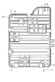
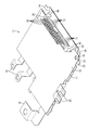
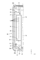
- the electrical junction box 10 has a circuit board 11, a control circuit board 33 disposed opposite to the circuit board 11 with a space therebetween, and the circuit board 11, and heat is radiated to the outside. And a case 45 for accommodating the circuit board 11 and the control circuit board 33 between the heat dissipating member 42.
- circuit board 11 As shown in FIG. 7, the circuit board 11 has a rectangular shape, and an electronic component (not shown) is mounted on a conductive path (not shown).
- the electronic component includes a switching element such as an FET (Field Effect Transistor), a capacitor, and the like.
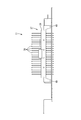
- the circuit board 11 includes an insulating substrate 12, a bus bar substrate 17 that is stacked on the insulating substrate 12, and a reinforcing plate 20 that is stacked on the insulating substrate 12 at a position different from the bus bar substrate 17.
- the insulating substrate 12 has a rectangular shape, and a conductive path made of copper foil or the like is formed by a printed wiring technique on an insulating plate made of an insulating material.
- the insulating substrate 12 includes a plurality of terminal insertion holes 13 through which the terminals 38 of the terminal module 37 are inserted, component insertion holes (not shown) for connecting the lead terminals of the electronic components to the bus bar substrate 17, and screws to the heat dissipation member 42.
- a through hole 15 through which a shaft portion of a metal screw 65 for fastening is passed is formed.
- Each terminal insertion hole 13 is connected to the conductive path of the insulating substrate 12, and a plurality of terminal insertion holes 13 are formed in a line.
- a plurality of component insertion holes are formed according to the position of the lead terminal 38 of the electronic component, and are composed of a large hole through which the bottom surface of the electronic component can be inserted and a small hole through which only the lead terminal can be inserted.
- the through-holes 15 are plural (one through-hole is shown in FIG. 7 and the other illustrations are omitted), and are circular shapes into which the shaft portion of the screw 65 can be inserted. It is arranged at the corner.
- the bus bar substrate 17 is composed of a plurality of plate-like bus bars 17A (see FIG. 11) formed by punching a metal plate material made of a copper alloy or the like in accordance with the shape of the conductive path, and the bus bars 17A are insulated at intervals. Affixed to the lower surface of the substrate 12 and fixed. Of the bus bar substrate 17, a through hole (not shown) through which a screw (not shown) for screwing is passed through the bus bar 17 ⁇ / b> A that overlaps with a through hole (not shown) of the insulating substrate 12. As shown in FIG. 7, the end portion of the bus bar substrate 17 is bent into a crank shape to form a connection terminal 19 connected to an external power supply terminal, output terminal, and coil (not shown).
- the reinforcing plate 20 has a plate shape that is long in the arrangement direction of the plurality of terminal insertion holes 13 overlapped with the rear end portion (left end portion in FIG. 11) of the insulating substrate 12.
- the insulating substrate 12 is disposed with a gap through a substrate exposed region 29 where the back surface of the insulating substrate 12 is exposed, and is fixed to the lower surface of the insulating substrate 12 with an adhesive.
- the reinforcing plate 20 is arranged on one end side in the arrangement direction of the terminals 38 and fixed to the heat radiating member 42 by being screwed with screws 65.
- the width of the reinforcing plate 20 is reduced from the fixing portion 21.
- the diameter-reduced portion 26 extending along the side edge of the substrate exposed region 29, and the diameter-increased portion 27, which is disposed on the other end side in the arrangement direction of the terminals 38 and whose width is increased from the diameter-reduced portion 26, Have
- the fixing portion 21 includes a circular through hole 22 into which a shaft portion of a screw 65 having a head portion and a shaft portion is inserted, a projecting piece 23 to be fitted into the recess 50 on the bottom surface of the case 45, and a side edge that is concave. And an engaging portion 24 that is notched and engages with the engaging pin 51 of the case 45.
- the through hole 22 is formed in the vicinity of the engaging portion 24. Specifically, the through hole 22 is located near the front edge on the opposite side of the engaging portion 24 in the front-rear direction (X-axis) and slightly more than the engaging portion 24 in the left-right direction (Y-axis). It is arranged on the protruding piece 23 side (one end side in the arrangement direction of the terminals 38).
- the projecting piece 23 is located in the vicinity of the through hole 22, and is disposed at one end of the reinforcing plate 20 in the arrangement direction of the terminals 38.
- the projecting piece 23 is The housing 45 is housed in a recess 50 formed on the bottom surface of the case 45.
- the outer edge portion from the base end of the projecting piece 23 to the engaging portion 24 is notched according to the bottom surface shape of the case 45.
- the engaging portion 24 has a shape in which the rear end portion of the fixed portion 21 is cut out in a semicircular shape. Of the edge portion of the engaging portion 24, the protruding piece 23 side protrudes rearward and the engaging pin 51. It is set as the receiving part 24A which receives.
- the reduced diameter portion 26 extends in the left-right direction with a constant width dimension.
- the enlarged diameter portion 27 includes a locked portion 28 that is locked to the case 45.
- the locked portion 28 stands up in a crank shape from the plate surface of the reinforcing plate 20 and extends to a position one step higher on the side.
- the periphery of the terminal insertion hole 13 on the back surface of the insulating substrate 12 is a substrate exposed region 29 where the bus bar substrate 17 and the reinforcing plate 20 are not overlapped and the back surface of the insulating substrate 12 is exposed and soldered.
- the substrate exposed region 29 extends along the arrangement direction of the plurality of terminals 38 and is formed with a certain width dimension.
- the insulating substrate 12 is affixed to the bus bar substrate 17 and the reinforcing plate 20 with an insulating adhesive 31.
- the adhesive 31 adheres between the insulating substrate 12 and the bus bar substrate 17 and between the insulating substrate 12 and the reinforcing plate 20 over the entire portion excluding the component insertion hole and the substrate exposed region 29.
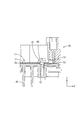
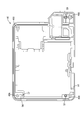
- Control circuit board 33 As shown in FIG. 5, the control circuit board 33 has a rectangular shape with a smaller area than the circuit board 11, and a conductive path made of copper foil or the like is printed on an insulating plate made of an insulating material.
- the control circuit board 33 the upper end side of the terminal 38 of the terminal module 37 is inserted into the through hole 62 and soldered, and the control housing 34 is fixed by screwing with a screw 61.
- the control housing 34 is made of synthetic resin and has an opening in a rectangular tube shape into which a mating connector housing can be fitted, and an L-shaped control terminal 36 is fixed.
- the conductive path of the circuit board 11 and the conductive path of the control circuit board 33 are connected by a plurality of terminals 38 of the terminal module 37.
- the terminal module 37 includes a plurality of terminals 38 arranged in a row and a connecting member 39 that connects the plurality of terminals 38.
- Each terminal 38 is made of copper, copper alloy, or the like and has the same shape.
- the connecting member 39 is made of an insulating synthetic resin, and has a plurality of terminals 38 and leg portions 40 placed on the circuit board 11.
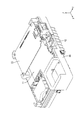
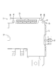
- the heat dissipating member 42 is made of a metal material having high thermal conductivity such as an aluminum alloy or a copper alloy. As shown in FIGS. 2 and 3, the upper surface side is flat and a large number of heat dissipating fins are arranged side by side on the lower surface side. Yes. A screw hole 53 that can be screwed with a screw 65 is formed at a predetermined depth on the upper surface of the heat dissipation member 42 at a position below the through hole 15 of the insulating substrate 12 and the through hole 22 of the reinforcing plate 20.
- the heat radiating member 42 is formed with a plurality of insertion holes 43 that are screwed to the holding member 46 at the positions of the four corners.
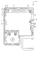
- the case 45 includes a synthetic resin holding member 46 placed on the upper surface of the heat radiating member 42, and a metal shield cover 60 mounted on the holding member 46. .
- the holding member 46 is provided along the peripheral edge of the heat radiating member 42, and a frame-like frame portion 47 that holds the circuit board 11 and the control circuit board 33 inside, and the shield cover 60.
- An attachment portion 56 is provided that can be attached to an end portion of an electric wire that is arranged on the outside and connected to an external power source (not shown).
- the frame portion 47 is partitioned at a portion where the choke coil 66 is accommodated.
- the upper part of the frame part 47 is provided with board fixing parts 48 and 49 to which the four corners of the control circuit board 33 are fixed.
- the pair of board fixing parts 48 arranged diagonally have a convex part inserted into the through hole 35 of the control circuit board 33, and the other pair of board fixing parts 49 are the through holes 35 of the control circuit board 33.
- a screw hole that can be screwed with a screw 61 is formed.
- the circuit board 11 can be mounted on the bottom surface (back surface) side of the frame portion 47. As shown in FIGS. 10 and 11, the recess 50 into which the protruding piece 23 of the reinforcing plate 20 is inserted, and the engaging portion 24, an engaging pin 51 that engages with 24, and a locking portion 52 that locks the locked portion 28 are provided.
- the concave portion 50 has a groove shape extending in the direction in which the protruding piece 23 protrudes.
- the engagement pin 51 has a cylindrical rod shape that rises in a direction orthogonal to the bottom surface of the frame portion 47.
- the engagement pin 51 can be positioned with its circular outer peripheral surface slidingly in contact with the engagement portion 24.
- the engaging pin 51 penetrates the heat radiating member 42 together with the guide pin 59 having the same shape as the engaging pin 51 formed at the end opposite to the engaging pin 51 on the back surface of the holding member 46. (It may be recessed on the upper surface of the member 42) and is inserted into the receiving portion 44, and can guide the movement in the assembling direction when the holding member 46 is assembled.
- the locking portion 52 is the upper surface of the bottom surface portion 54 that protrudes in a plate shape in the horizontal direction on the bottom surface of the frame portion 47 (see FIG. 6). The position on the side of the locking part 52 in the circuit board 11 is held.
- boss portions 46A for screwing screws (not shown) through the insertion holes 43 from the heat radiating member 42 side to the holding member 46 are formed at four corner positions.
- the boss portion 46A has a screw hole, and the relative position between the holding member 46 and the heat dissipation member 42 is fixed by screwing to the boss portion 46A.
- the attachment part 56 partitions the terminal connected to the power supply side from the outside. Electric power from an external power source is supplied to the circuit board 11 via a terminal in the mounting portion 56.
- a connector housing 55 in which the connection terminals 19 are arranged is mounted.
- the shield cover 60 is formed by punching and bending a plate-like metal made of aluminum or the like, and the lower end portion is fixed to the heat dissipation member 42 by screwing to the heat dissipation member 42 with screws 64. At the same time, the shield cover 60 is connected to the ground via the heat dissipation member 42.
- the assembly of the electrical junction box 10 will be described.
- the adhesive 31 is applied to the insulating substrate 12 and the bus bar substrate 17 and the reinforcing plate 20 are overlapped to form the circuit board 11, and the terminal module 37 is mounted on the circuit board 11 and inserted into the terminal insertion holes 13 of the circuit board 11.
- the lower ends of the plurality of terminals 38 are flow soldered (FIG. 7).
- the engaging pin 51 of the holding member 46 is aligned with the engaging portion 24 of the circuit board 11 to engage the engaging portion 24 with the engaging pin 51, and the projecting piece 23 is recessed with the concave portion 50 of the holding member 46.
- the circuit board 11 is fitted to the bottom surface of the frame portion 47 (FIG. 11).
- the heat radiating member 42 is disposed on the back side of the holding member 46 into which the circuit board 11 is fitted, and the engaging pin 51 and the guide pin 59 are inserted into the receiving portion 44 of the heat radiating member 42, and the heat radiating member 42 is connected to the circuit board. 11 and the holding member 46, the screw hole 53 of the heat dissipation member 42 overlaps the through hole 15 of the insulating substrate 12 and the through hole 22 of the reinforcing plate 20. Then, the circuit board 11 is screwed into the screw hole 53 of the heat radiating member 42 through the screw 65 through the through hole 15 and the through hole 22 from the upper surface side of the circuit board 11 (FIG. 3), and the insertion hole from the back surface side of the heat radiating member 42.
- the heat radiating member 42 is screwed to the holding member 46 through 43.
- the control circuit board 33 is screwed to the board fixing portions 48 and 49, and the upper ends of the terminals 38 are flow soldered (FIG. 4).
- the electrical connection box 10 is formed by covering the shield cover 60 and screwing it onto the heat dissipation member 42 with screws 64 (FIG. 1).
- the electrical junction box 10 is formed in an insulating substrate 12 having a conductive path formed on an insulating plate, a bus bar 17A attached to the insulating substrate 12 to form a conductive path, and a region of the insulating substrate 12 where the bus bar 17A is not attached.
- the reinforcing plate 20 that is pasted and formed with the through hole 22 through which the shaft portion of the screw 65 is formed, the terminal 38 that is soldered to the insulating substrate 12, and the surface of the reinforcing plate 20 opposite to the insulating substrate 12 are overlapped.
- An engaging portion 24 is provided in which the through hole 22 and the screw hole 53 are aligned by engaging with the holding member 46.
- the insulating substrate 12 can be reinforced by the reinforcing plate 20, deformation of the insulating substrate 12 due to heat when soldering the terminals 38 can be suppressed.
- the engaging portion 24 of the reinforcing plate 20 is engaged with the holding member 46 so that the through hole 22 and the screw hole 53 are aligned, the reinforcing plate 20 is screwed to the heat radiating member 42 in this state. Then, the position of the insulating substrate 12 with respect to the heat radiating member 42 can be fixed via the reinforcing plate 20. Therefore, it is possible to easily position the insulating substrate 12 with respect to the heat dissipation member 42 while reinforcing the insulating substrate 12.
- the engaging part 24 is provided in the vicinity of the through-hole 22, it can raise the precision of position alignment. Furthermore, since the engaging part 24 is formed by cutting out the peripheral edge of the reinforcing plate 20, the shape of the engaging part 24 can be simplified.
- the holding member 46 includes the engaging pin 51 that engages with the engaging portion 24, the engaging portion 24 can be easily engaged with the holding member 46.
- the reinforcing plate 20 includes the projecting piece 23 fitted in the holding member 46 in the vicinity of the through hole 22, the direction (front-rear direction) orthogonal to the arrangement direction (left-right direction) of the plurality of terminals 38. Can be positioned.
- the engaging pin 51 is inserted into the receiving portion 44 of the heat radiating member 42 so that the engaging pin 51 does not come into contact with the heat radiating member 42 even if the protruding dimension of the engaging pin 51 is increased. Therefore, the protruding dimension of the engaging pin 51 can be increased so that the engaging pin 51 can easily engage with the engaging portion 24.
- the insulating substrate 12 includes a terminal insertion hole 13 into which the terminal 38 is inserted and soldered, and the reinforcing plate 20 does not overlap the bus bar 17A in the region including the terminal insertion hole 13 in the insulating substrate 12. Is disposed along the edge of the exposed substrate exposed region 29. In this way, the reinforcing plate 20 can reinforce the position along the edge of the substrate exposed region 29 where the bus bar 17A cannot be superimposed on the insulating substrate 12 in order to insulate it from the outside.
- the terminal 38 includes a plurality of terminals, and a terminal module 37 in which the plurality of terminals 38 are connected by a connecting member 39.
- the connecting member 39 is provided on a surface of the insulating substrate 12 opposite to the surface on which the reinforcing plate 20 overlaps. It is in contact. By doing so, the connecting member 39 for connecting the plurality of terminals 38 is brought into contact with the insulating substrate 12, so that the surface of the insulating substrate 12 opposite to the surface on which the reinforcing plate 20 overlaps is connected by the connecting member 39. Can be supported.
- the present invention is not limited to the embodiments described with reference to the above description and drawings.
- the reinforcing plate 20 is made of the same material as the bus bar 17A, but may be made of a different material.
- the reinforcing plate is not limited to metal but may be formed of resin.
- the holding member 46 may directly hold the insulating substrate 12, the bus bar 17 ⁇ / b> A, and the reinforcing plate 20, or may indirectly hold them via other members.
- the shape and position for the engaging portion 24 to engage with the holding member 46 are not limited to the above embodiment.
- the engaging portion may be provided at a position different from the engaging portion 24.
- it is not restricted to the structure which provides the protruding member like an engagement pin, You may engage the engaging part 24 with the part which does not protrude.
- the insulating substrate 12 is overlaid on the portion of the reinforcing plate 20 that is screwed with the screw 65, but the insulating substrate 12 is not overlaid on the screwed portion (the edge of the through hole 22). Only the reinforcing plate 20 may be screwed to the heat radiating member 42. Even in this case, if the reinforcing plate 20 is fixed to the insulating substrate 12 with an adhesive or the like, the insulating substrate 12 can be aligned with the heat dissipation member 42.
Abstract
This electrical junction box (10) comprises: an insulating substrate (12) having an electroconductive path formed on an insulating plate; a bus bar (17A) that is bonded to the insulating substrate (12) and that forms an electroconductive path; a reinforcement plate (20) that is bonded to a region in the insulating substrate (12) where the bus bar (17A) is not bonded, the reinforcement plate having formed therein a through hole (22) through which a shaft part of a screw (65) is passed; a terminal (38) that is soldered to the insulating substrate (12); a heat-dissipating member (42) that is superposed on a surface of the reinforcement plate (20) on the opposite side from the insulating substrate (12), the heat-dissipating member having formed therein a screw hole (53) into which the screw (65) is screwed; and a retaining member (46) that retains the respective positions of the insulating substrate (12), the bus bar (17A), and the reinforcement plate (20). The reinforcement plate (20) includes an engagement part (24) that positions the through hole (22) and the screw hole (53) with respect to one another by engaging with the retaining member (46).
Description
本発明は、電気接続箱に関する。
The present invention relates to an electrical junction box.
従来、絶縁基板とバスバー基板とが重ねられ、放熱部材に対して固定された電気接続箱が知られている。特許文献1は、複数のバスバーからなるバスバー構成板とプリント基板とが積層された回路構成体と、この回路構成体を内蔵したケースとを備えている。プリント基板上にはリレー等の電気部品が実装されており、ケースの底部には放熱板が配置されている。バスバー構成板は、導電路の形状に応じた多数のバスバーからなる。バスバー構成板が板厚の薄いプリント基板に重ねられているため、プリント基板の強度が補強されている。
Conventionally, an electrical junction box in which an insulating substrate and a bus bar substrate are stacked and fixed to a heat radiating member is known. Patent Document 1 includes a circuit configuration body in which a bus bar configuration board composed of a plurality of bus bars and a printed board are stacked, and a case in which the circuit configuration body is built. Electrical components such as relays are mounted on the printed circuit board, and a heat sink is disposed at the bottom of the case. The bus bar constituting plate is composed of a large number of bus bars corresponding to the shape of the conductive path. Since the bus bar constituting plate is superimposed on the thin printed board, the strength of the printed board is reinforced.
ところで、プリント基板のうちバスバー構成板が重なっていない領域はその強度を充分に確保し難いため、半田付けの熱で変形することが懸念される。一方、プリント基板の変形等を抑制するために、プリント基板のうちバスバー構成板が重ならない位置に補強板を重ねることでプリント基板を補強することが考えられる。この場合、プリント基板の補強だけでなく、放熱板に対するプリント基板の位置決めを容易にできることが望ましい。
By the way, there is a concern that the area of the printed circuit board where the bus bar constituent plates do not overlap is difficult to secure its strength, and is deformed by the heat of soldering. On the other hand, in order to suppress deformation or the like of the printed circuit board, it is conceivable to reinforce the printed circuit board by overlapping a reinforcing plate at a position where the bus bar constituting plate does not overlap in the printed circuit board. In this case, it is desirable not only to reinforce the printed circuit board but also to facilitate positioning of the printed circuit board with respect to the heat sink.
本発明は上記のような事情に基づいて完成されたものであって、絶縁基板を補強しつつ放熱部材に対する絶縁基板の位置決めを容易に行うことを目的とする。
The present invention has been completed based on the above circumstances, and an object thereof is to easily position the insulating substrate with respect to the heat radiating member while reinforcing the insulating substrate.
本発明の電気接続箱は、絶縁板に導電路が形成された絶縁基板と、前記絶縁基板に貼り付けられ、導電路を形成するバスバーと、前記絶縁基板における前記バスバーが貼り付けられない領域に貼り付けられ、ネジの軸部を通す通し孔が形成された補強板と、前記絶縁基板に半田付けされる端子と、前記補強板における前記絶縁基板とは反対側の面に重ねられ、前記ネジでネジ留めするためのネジ孔が形成された放熱部材と、前記絶縁基板、前記バスバー及び前記補強板の位置を保持する保持部材と、を備え、前記補強板は、前記保持部材に係合することで前記通し孔と前記ネジ孔との位置合わせがされる係合部を備える。
The electrical junction box of the present invention includes an insulating substrate in which a conductive path is formed on an insulating plate, a bus bar that is attached to the insulating substrate and forms a conductive path, and a region in the insulating substrate where the bus bar is not attached. The reinforcing plate formed with a through-hole through which the shaft portion of the screw is pasted, the terminal to be soldered to the insulating substrate, and the surface of the reinforcing plate opposite to the insulating substrate are overlapped, and the screw A heat radiating member in which screw holes for screwing are formed, and a holding member that holds the positions of the insulating substrate, the bus bar, and the reinforcing plate, and the reinforcing plate engages with the holding member Thus, an engagement portion is provided that aligns the through hole and the screw hole.
本構成によれば、補強板の係合部が保持部材に係合することで通し孔とネジ孔との位置合わせがされるため、この状態で、補強板を放熱部材にネジ留めすれば放熱部材に対する絶縁基板の位置を補強板を介して固定することができる。よって、絶縁基板を補強しつつ放熱部材に対する絶縁基板の位置決めを容易に行うことができる。
According to this configuration, since the engaging portion of the reinforcing plate engages with the holding member, the through hole and the screw hole are aligned, and in this state, if the reinforcing plate is screwed to the heat radiating member, heat dissipation is performed. The position of the insulating substrate with respect to the member can be fixed via the reinforcing plate. Therefore, it is possible to easily position the insulating substrate with respect to the heat dissipation member while reinforcing the insulating substrate.
本発明の実施態様としては以下の態様が好ましい。
・前記係合部は、前記通し孔の近傍に設けられている。
このようにすれば、位置合わせの精度を高めることができる。 As embodiments of the present invention, the following embodiments are preferable.
-The engaging part is provided in the vicinity of the through hole.
In this way, alignment accuracy can be increased.
・前記係合部は、前記通し孔の近傍に設けられている。
このようにすれば、位置合わせの精度を高めることができる。 As embodiments of the present invention, the following embodiments are preferable.
-The engaging part is provided in the vicinity of the through hole.
In this way, alignment accuracy can be increased.
・前記係合部は、前記補強板における周縁を切り欠いて形成されている。
このようにすれば、係合部の形状を簡素化することができる。 -The said engaging part is formed by notching the periphery in the said reinforcement board.
If it does in this way, the shape of an engaging part can be simplified.
このようにすれば、係合部の形状を簡素化することができる。 -The said engaging part is formed by notching the periphery in the said reinforcement board.
If it does in this way, the shape of an engaging part can be simplified.
・前記保持部材は、前記係合部に係合する係合ピンを備えている。
このようにすれば、係合部を保持部材に容易に係合させることができる。 The holding member includes an engagement pin that engages with the engagement portion.
If it does in this way, an engaging part can be easily engaged with a holding member.
このようにすれば、係合部を保持部材に容易に係合させることができる。 The holding member includes an engagement pin that engages with the engagement portion.
If it does in this way, an engaging part can be easily engaged with a holding member.
・前記放熱部材は、前記係合ピンが挿通される受け部を有する。
このようにすれば、係合ピンが放熱部材の受け部に挿通されることで、係合ピンの突出寸法を大きくしても係合ピンが放熱部材に当接しないようにすることができるため、係合ピンの突出寸法を大きくして係合ピンが係合部に係合しやすいようにすることが可能になる。 -The said heat radiating member has a receiving part in which the said engagement pin is penetrated.
By doing so, the engagement pin is inserted into the receiving portion of the heat dissipation member, so that the engagement pin can be prevented from coming into contact with the heat dissipation member even if the protrusion dimension of the engagement pin is increased. It is possible to increase the protruding dimension of the engaging pin so that the engaging pin can be easily engaged with the engaging portion.
・前記補強板は、前記通し孔の近傍に前記保持部材に嵌め入れられる突片を備えている。
The reinforcing plate includes a protruding piece that is fitted into the holding member in the vicinity of the through hole.
・前記絶縁基板は、前記端子が挿通されて半田付けされる端子挿通孔を備え、前記補強板は、前記絶縁基板における前記端子挿通孔を含む領域で前記バスバーが重ならない基板露出領域の端縁の沿うように配されている。
外部と絶縁するためにバスバーを絶縁基板に重ねることができない基板露出領域の端縁の沿う位置を補強板で補強することができる。 The insulating substrate includes a terminal insertion hole into which the terminal is inserted and soldered, and the reinforcing plate is an edge of the substrate exposed region where the bus bar does not overlap in the region including the terminal insertion hole in the insulating substrate. It is arranged along.
The position along the edge of the substrate exposed region where the bus bar cannot be superimposed on the insulating substrate to insulate from the outside can be reinforced with the reinforcing plate.
・前記端子は複数であって、前記複数の端子が連結部材で連結された端子モジュールを備え、前記連結部材は、前記絶縁基板における前記補強板が重なる面とは反対側の面に当接している。
The terminal includes a plurality of terminals and a terminal module in which the plurality of terminals are connected by a connecting member, and the connecting member is in contact with a surface of the insulating substrate opposite to a surface on which the reinforcing plate overlaps. Yes.
本発明によれば、絶縁基板を補強しつつ放熱部材に対する絶縁基板の位置決めを容易に行うことができる。
According to the present invention, it is possible to easily position the insulating substrate with respect to the heat radiating member while reinforcing the insulating substrate.
<実施形態>
実施形態を図1ないし図11を参照しつつ説明する。
電気接続箱10は、例えば電気自動車やハイブリット自動車等の車両のバッテリ等の電源とランプ等の車載電装品や駆動モータ等からなる負荷との間の電力供給経路に配され、例えばDC-DCコンバータやインバータ等に用いることができる。以下では、上下方向(Z軸)及び左右方向(Y軸)については、図3の方向を基準とし、前後方向(X軸)については図6の左方を前方、右方を後方として説明する。 <Embodiment>
The embodiment will be described with reference to FIGS.
Theelectric junction box 10 is arranged in a power supply path between a power source such as a battery of a vehicle such as an electric vehicle or a hybrid vehicle and a load including an in-vehicle electrical component such as a lamp or a drive motor, for example, a DC-DC converter. It can be used for inverters and the like. Hereinafter, the vertical direction (Z-axis) and the horizontal direction (Y-axis) will be described with reference to the direction of FIG. 3, and the front-back direction (X-axis) will be described with the left side of FIG. .
実施形態を図1ないし図11を参照しつつ説明する。
電気接続箱10は、例えば電気自動車やハイブリット自動車等の車両のバッテリ等の電源とランプ等の車載電装品や駆動モータ等からなる負荷との間の電力供給経路に配され、例えばDC-DCコンバータやインバータ等に用いることができる。以下では、上下方向(Z軸)及び左右方向(Y軸)については、図3の方向を基準とし、前後方向(X軸)については図6の左方を前方、右方を後方として説明する。 <Embodiment>
The embodiment will be described with reference to FIGS.
The
(電気接続箱10)
電気接続箱10は、図1,図4に示すように、回路基板11と、回路基板11に間隔を空けて対向配置された制御回路基板33と、回路基板11が載置され、外部に放熱するための放熱部材42と、回路基板11及び制御回路基板33を放熱部材42との間に収容するケース45と、を備えている。 (Electric junction box 10)
As shown in FIGS. 1 and 4, theelectrical junction box 10 has a circuit board 11, a control circuit board 33 disposed opposite to the circuit board 11 with a space therebetween, and the circuit board 11, and heat is radiated to the outside. And a case 45 for accommodating the circuit board 11 and the control circuit board 33 between the heat dissipating member 42.
電気接続箱10は、図1,図4に示すように、回路基板11と、回路基板11に間隔を空けて対向配置された制御回路基板33と、回路基板11が載置され、外部に放熱するための放熱部材42と、回路基板11及び制御回路基板33を放熱部材42との間に収容するケース45と、を備えている。 (Electric junction box 10)
As shown in FIGS. 1 and 4, the
(回路基板11)
回路基板11は、図7に示すように、長方形状であって、図示しない導電路に図示しない電子部品が実装される。電子部品は、FET(Field Effect Transistor)等のスイッチング素子やコンデンサ等からなる。回路基板11は、絶縁基板12と、絶縁基板12に重ねられるバスバー基板17と、絶縁基板12におけるバスバー基板17とは異なる位置に重ねられる補強板20と、を備えている。 (Circuit board 11)
As shown in FIG. 7, thecircuit board 11 has a rectangular shape, and an electronic component (not shown) is mounted on a conductive path (not shown). The electronic component includes a switching element such as an FET (Field Effect Transistor), a capacitor, and the like. The circuit board 11 includes an insulating substrate 12, a bus bar substrate 17 that is stacked on the insulating substrate 12, and a reinforcing plate 20 that is stacked on the insulating substrate 12 at a position different from the bus bar substrate 17.
回路基板11は、図7に示すように、長方形状であって、図示しない導電路に図示しない電子部品が実装される。電子部品は、FET(Field Effect Transistor)等のスイッチング素子やコンデンサ等からなる。回路基板11は、絶縁基板12と、絶縁基板12に重ねられるバスバー基板17と、絶縁基板12におけるバスバー基板17とは異なる位置に重ねられる補強板20と、を備えている。 (Circuit board 11)
As shown in FIG. 7, the
(絶縁基板12)
絶縁基板12は、長方形状であって、絶縁材料からなる絶縁板に銅箔等からなる導電路がプリント配線技術により形成されている。絶縁基板12は、端子モジュール37の端子38が挿通される複数の端子挿通孔13と、電子部品のリード端子をバスバー基板17に接続するため部品挿通孔(図示しない)と、放熱部材42にネジ留めするための金属製のネジ65の軸部を通す通し穴15と、が貫通形成されている。 (Insulating substrate 12)
Theinsulating substrate 12 has a rectangular shape, and a conductive path made of copper foil or the like is formed by a printed wiring technique on an insulating plate made of an insulating material. The insulating substrate 12 includes a plurality of terminal insertion holes 13 through which the terminals 38 of the terminal module 37 are inserted, component insertion holes (not shown) for connecting the lead terminals of the electronic components to the bus bar substrate 17, and screws to the heat dissipation member 42. A through hole 15 through which a shaft portion of a metal screw 65 for fastening is passed is formed.
絶縁基板12は、長方形状であって、絶縁材料からなる絶縁板に銅箔等からなる導電路がプリント配線技術により形成されている。絶縁基板12は、端子モジュール37の端子38が挿通される複数の端子挿通孔13と、電子部品のリード端子をバスバー基板17に接続するため部品挿通孔(図示しない)と、放熱部材42にネジ留めするための金属製のネジ65の軸部を通す通し穴15と、が貫通形成されている。 (Insulating substrate 12)
The
各端子挿通孔13は、絶縁基板12の導電路に連なっており、複数の端子挿通孔13が一列に並んで形成されている。部品挿通孔は、電子部品のリード端子38の位置に応じて複数形成されており、電子部品の底面を挿通可能な面積が大きい孔とリード端子のみを挿通可能な小さい孔とからなる。通し穴15は、複数(図7では1つの通し孔を図示し、他の図示は省略)であって、ネジ65の軸部を挿通可能な円形状であって、絶縁基板12の周縁部や角部の位置に配されている。
Each terminal insertion hole 13 is connected to the conductive path of the insulating substrate 12, and a plurality of terminal insertion holes 13 are formed in a line. A plurality of component insertion holes are formed according to the position of the lead terminal 38 of the electronic component, and are composed of a large hole through which the bottom surface of the electronic component can be inserted and a small hole through which only the lead terminal can be inserted. The through-holes 15 are plural (one through-hole is shown in FIG. 7 and the other illustrations are omitted), and are circular shapes into which the shaft portion of the screw 65 can be inserted. It is arranged at the corner.
(バスバー基板17)
バスバー基板17は、銅合金等からなる金属板材を導電路の形状に応じて打ち抜いて形成した複数の板状のバスバー17A(図11参照)から構成され、各バスバー17A間は間隔を空けて絶縁基板12の下面に貼り付けられて固定されている。バスバー基板17のうち、絶縁基板12の通し穴(図示しない)に重なるバスバー17Aには、ネジ留めするためのネジ(図示しない)を通す通し穴(図示しない)が貫通形成されている。バスバー基板17の端部は、図7に示すように、クランク状に屈曲されて外部の図示しない電源端子や出力端子やコイルに接続される接続端子19を形成している。 (Bus bar substrate 17)
Thebus bar substrate 17 is composed of a plurality of plate-like bus bars 17A (see FIG. 11) formed by punching a metal plate material made of a copper alloy or the like in accordance with the shape of the conductive path, and the bus bars 17A are insulated at intervals. Affixed to the lower surface of the substrate 12 and fixed. Of the bus bar substrate 17, a through hole (not shown) through which a screw (not shown) for screwing is passed through the bus bar 17 </ b> A that overlaps with a through hole (not shown) of the insulating substrate 12. As shown in FIG. 7, the end portion of the bus bar substrate 17 is bent into a crank shape to form a connection terminal 19 connected to an external power supply terminal, output terminal, and coil (not shown).
バスバー基板17は、銅合金等からなる金属板材を導電路の形状に応じて打ち抜いて形成した複数の板状のバスバー17A(図11参照)から構成され、各バスバー17A間は間隔を空けて絶縁基板12の下面に貼り付けられて固定されている。バスバー基板17のうち、絶縁基板12の通し穴(図示しない)に重なるバスバー17Aには、ネジ留めするためのネジ(図示しない)を通す通し穴(図示しない)が貫通形成されている。バスバー基板17の端部は、図7に示すように、クランク状に屈曲されて外部の図示しない電源端子や出力端子やコイルに接続される接続端子19を形成している。 (Bus bar substrate 17)
The
(補強板20)
補強板20は、図11に示すように、絶縁基板12の後端部(図11の左端部)に重ねられた複数の端子挿通孔13の並び方向に長い板状であって、バスバー17Aとの間に絶縁基板12の裏面が露出した基板露出領域29を介して間隔を空けて配置されており、絶縁基板12の下面に接着剤で貼り付けられて固定されている。この補強板20は、端子38の並び方向の一方の端部側に配されて放熱部材42にネジ65でネジ留めされて固定される固定部21と、固定部21から幅寸法が縮径され、基板露出領域29の側縁に沿って延びる縮径部26と、端子38の並び方向の他方の端部側に配され、縮径部26から幅寸法が拡径された拡径部27とを有する。 (Reinforcing plate 20)
As shown in FIG. 11, thereinforcing plate 20 has a plate shape that is long in the arrangement direction of the plurality of terminal insertion holes 13 overlapped with the rear end portion (left end portion in FIG. 11) of the insulating substrate 12. In this case, the insulating substrate 12 is disposed with a gap through a substrate exposed region 29 where the back surface of the insulating substrate 12 is exposed, and is fixed to the lower surface of the insulating substrate 12 with an adhesive. The reinforcing plate 20 is arranged on one end side in the arrangement direction of the terminals 38 and fixed to the heat radiating member 42 by being screwed with screws 65. The width of the reinforcing plate 20 is reduced from the fixing portion 21. The diameter-reduced portion 26 extending along the side edge of the substrate exposed region 29, and the diameter-increased portion 27, which is disposed on the other end side in the arrangement direction of the terminals 38 and whose width is increased from the diameter-reduced portion 26, Have
補強板20は、図11に示すように、絶縁基板12の後端部(図11の左端部)に重ねられた複数の端子挿通孔13の並び方向に長い板状であって、バスバー17Aとの間に絶縁基板12の裏面が露出した基板露出領域29を介して間隔を空けて配置されており、絶縁基板12の下面に接着剤で貼り付けられて固定されている。この補強板20は、端子38の並び方向の一方の端部側に配されて放熱部材42にネジ65でネジ留めされて固定される固定部21と、固定部21から幅寸法が縮径され、基板露出領域29の側縁に沿って延びる縮径部26と、端子38の並び方向の他方の端部側に配され、縮径部26から幅寸法が拡径された拡径部27とを有する。 (Reinforcing plate 20)
As shown in FIG. 11, the
固定部21は、頭部と軸部を有するネジ65の軸部が挿通される円形状の通し孔22と、ケース45の底面の凹部50に嵌め入れられる突片23と、側縁が凹状に切り欠かれてケース45の係合ピン51に係合する係合部24とを備えている。
The fixing portion 21 includes a circular through hole 22 into which a shaft portion of a screw 65 having a head portion and a shaft portion is inserted, a projecting piece 23 to be fitted into the recess 50 on the bottom surface of the case 45, and a side edge that is concave. And an engaging portion 24 that is notched and engages with the engaging pin 51 of the case 45.
通し孔22は、係合部24の近傍に形成されている。具体的には、通し孔22は、前後方向(X軸)については、係合部24とは反対側の前端縁寄りの位置で、左右方向(Y軸)には係合部24よりもやや突片23側(端子38の並び方向の一方の端部側)に配されている。突片23は、通し孔22の近傍に位置し、補強板20における端子38の並び方向の一方の端部に配されており、回路基板11がケース45に装着されると、突片23は、ケース45の底面に形成された凹部50に収容される。突片23の基端から係合部24に至る外縁部は、ケース45の底面形状に応じて切り欠かれている。
The through hole 22 is formed in the vicinity of the engaging portion 24. Specifically, the through hole 22 is located near the front edge on the opposite side of the engaging portion 24 in the front-rear direction (X-axis) and slightly more than the engaging portion 24 in the left-right direction (Y-axis). It is arranged on the protruding piece 23 side (one end side in the arrangement direction of the terminals 38). The projecting piece 23 is located in the vicinity of the through hole 22, and is disposed at one end of the reinforcing plate 20 in the arrangement direction of the terminals 38. When the circuit board 11 is attached to the case 45, the projecting piece 23 is The housing 45 is housed in a recess 50 formed on the bottom surface of the case 45. The outer edge portion from the base end of the projecting piece 23 to the engaging portion 24 is notched according to the bottom surface shape of the case 45.
係合部24は、固定部21の後端部を半円形状に切り欠いた形状とされており、係合部24の縁部のうち、突片23側は後方に突き出て係合ピン51を受ける受け部24Aとされている。縮径部26は、一定の幅寸法で左右方向に延びている。拡径部27は、ケース45に係止される被係止部28を備えている。被係止部28は、補強板20の板面からクランク状に起立して側方の一段高い位置に延びている。
The engaging portion 24 has a shape in which the rear end portion of the fixed portion 21 is cut out in a semicircular shape. Of the edge portion of the engaging portion 24, the protruding piece 23 side protrudes rearward and the engaging pin 51. It is set as the receiving part 24A which receives. The reduced diameter portion 26 extends in the left-right direction with a constant width dimension. The enlarged diameter portion 27 includes a locked portion 28 that is locked to the case 45. The locked portion 28 stands up in a crank shape from the plate surface of the reinforcing plate 20 and extends to a position one step higher on the side.
絶縁基板12の裏面における端子挿通孔13の周囲は、バスバー基板17や補強板20が重ねられず、絶縁基板12の裏面が露出して半田付けされる基板露出領域29とされている。基板露出領域29は、複数の端子38の並び方向に沿って延び、一定の幅寸法で形成されている。
The periphery of the terminal insertion hole 13 on the back surface of the insulating substrate 12 is a substrate exposed region 29 where the bus bar substrate 17 and the reinforcing plate 20 are not overlapped and the back surface of the insulating substrate 12 is exposed and soldered. The substrate exposed region 29 extends along the arrangement direction of the plurality of terminals 38 and is formed with a certain width dimension.
絶縁基板12は、バスバー基板17や補強板20に、絶縁性の接着剤31で貼り付けられている。接着剤31は、部品挿通孔や基板露出領域29を除いた全体に亘って絶縁基板12とバスバー基板17との間、及び、絶縁基板12と補強板20との間を接着している。
The insulating substrate 12 is affixed to the bus bar substrate 17 and the reinforcing plate 20 with an insulating adhesive 31. The adhesive 31 adheres between the insulating substrate 12 and the bus bar substrate 17 and between the insulating substrate 12 and the reinforcing plate 20 over the entire portion excluding the component insertion hole and the substrate exposed region 29.
(制御回路基板33)
制御回路基板33は、図5に示すように、回路基板11よりも面積が小さい長方形状であって、絶縁材料からなる絶縁板に銅箔等からなる導電路がプリント配線されている。制御回路基板33は、端子モジュール37の端子38の上端側がスルーホール62に挿通されて半田付けされ、制御用ハウジング34がネジ61でネジ留めされて固定されている。制御用ハウジング34は、合成樹脂製で、相手側のコネクタハウジングを嵌合可能な角筒状に開口しており、L字状の制御端子36が固定されている。回路基板11の導電路と制御回路基板33の導電路との間は、端子モジュール37の複数の端子38により接続される。 (Control circuit board 33)
As shown in FIG. 5, thecontrol circuit board 33 has a rectangular shape with a smaller area than the circuit board 11, and a conductive path made of copper foil or the like is printed on an insulating plate made of an insulating material. In the control circuit board 33, the upper end side of the terminal 38 of the terminal module 37 is inserted into the through hole 62 and soldered, and the control housing 34 is fixed by screwing with a screw 61. The control housing 34 is made of synthetic resin and has an opening in a rectangular tube shape into which a mating connector housing can be fitted, and an L-shaped control terminal 36 is fixed. The conductive path of the circuit board 11 and the conductive path of the control circuit board 33 are connected by a plurality of terminals 38 of the terminal module 37.
制御回路基板33は、図5に示すように、回路基板11よりも面積が小さい長方形状であって、絶縁材料からなる絶縁板に銅箔等からなる導電路がプリント配線されている。制御回路基板33は、端子モジュール37の端子38の上端側がスルーホール62に挿通されて半田付けされ、制御用ハウジング34がネジ61でネジ留めされて固定されている。制御用ハウジング34は、合成樹脂製で、相手側のコネクタハウジングを嵌合可能な角筒状に開口しており、L字状の制御端子36が固定されている。回路基板11の導電路と制御回路基板33の導電路との間は、端子モジュール37の複数の端子38により接続される。 (Control circuit board 33)
As shown in FIG. 5, the
(端子モジュール37)
端子モジュール37は、1列に並んだ複数の端子38と、複数の端子38を連結する連結部材39とを備えている。各端子38は、銅や銅合金等からなり、同一形状である。連結部材39は、絶縁性の合成樹脂からなり、複数の端子38が固定されるとともに、回路基板11に載置される脚部40を有する。 (Terminal module 37)
Theterminal module 37 includes a plurality of terminals 38 arranged in a row and a connecting member 39 that connects the plurality of terminals 38. Each terminal 38 is made of copper, copper alloy, or the like and has the same shape. The connecting member 39 is made of an insulating synthetic resin, and has a plurality of terminals 38 and leg portions 40 placed on the circuit board 11.
端子モジュール37は、1列に並んだ複数の端子38と、複数の端子38を連結する連結部材39とを備えている。各端子38は、銅や銅合金等からなり、同一形状である。連結部材39は、絶縁性の合成樹脂からなり、複数の端子38が固定されるとともに、回路基板11に載置される脚部40を有する。 (Terminal module 37)
The
(放熱部材42)
放熱部材42は、アルミニウム合金や銅合金等の熱伝導性が高い金属材料からなり、図2,図3に示すように、上面側が平坦で、下面側に多数の放熱フィンが並んで配されている。放熱部材42の上面には、絶縁基板12の通し穴15や補強板20の通し孔22に連なる下方の位置にネジ65でネジ留め可能なネジ孔53が所定の深さで形成されている。ネジ65を絶縁基板12の上から絶縁基板12及び補強板20を挟んで放熱部材42に固定することで、絶縁基板12、補強板20及び放熱部材42間の位置が固定される。
また、放熱部材42には、保持部材46にネジ留めするための複数の挿通穴43が四隅の位置に貫通形成されている。 (Heat dissipation member 42)
Theheat dissipating member 42 is made of a metal material having high thermal conductivity such as an aluminum alloy or a copper alloy. As shown in FIGS. 2 and 3, the upper surface side is flat and a large number of heat dissipating fins are arranged side by side on the lower surface side. Yes. A screw hole 53 that can be screwed with a screw 65 is formed at a predetermined depth on the upper surface of the heat dissipation member 42 at a position below the through hole 15 of the insulating substrate 12 and the through hole 22 of the reinforcing plate 20. By fixing the screw 65 from above the insulating substrate 12 to the heat radiating member 42 with the insulating substrate 12 and the reinforcing plate 20 interposed therebetween, the positions between the insulating substrate 12, the reinforcing plate 20 and the heat radiating member 42 are fixed.
Further, theheat radiating member 42 is formed with a plurality of insertion holes 43 that are screwed to the holding member 46 at the positions of the four corners.
放熱部材42は、アルミニウム合金や銅合金等の熱伝導性が高い金属材料からなり、図2,図3に示すように、上面側が平坦で、下面側に多数の放熱フィンが並んで配されている。放熱部材42の上面には、絶縁基板12の通し穴15や補強板20の通し孔22に連なる下方の位置にネジ65でネジ留め可能なネジ孔53が所定の深さで形成されている。ネジ65を絶縁基板12の上から絶縁基板12及び補強板20を挟んで放熱部材42に固定することで、絶縁基板12、補強板20及び放熱部材42間の位置が固定される。
また、放熱部材42には、保持部材46にネジ留めするための複数の挿通穴43が四隅の位置に貫通形成されている。 (Heat dissipation member 42)
The
Further, the
(ケース45)
ケース45は、図1に示すように、放熱部材42の上面に載置される合成樹脂製の保持部材46と、保持部材46の上に装着される金属製のシールドカバー60とを備えている。 (Case 45)
As shown in FIG. 1, thecase 45 includes a synthetic resin holding member 46 placed on the upper surface of the heat radiating member 42, and a metal shield cover 60 mounted on the holding member 46. .
ケース45は、図1に示すように、放熱部材42の上面に載置される合成樹脂製の保持部材46と、保持部材46の上に装着される金属製のシールドカバー60とを備えている。 (Case 45)
As shown in FIG. 1, the
(保持部材46)
保持部材46は、図5に示すように、放熱部材42の周縁部に沿うように設けられ、内側に回路基板11及び制御回路基板33を保持するフレーム状のフレーム部47と、シールドカバー60の外側に配され、外部の図示しない電源側に接続された電線の端末部を取付可能な取付部56とを備えている。フレーム部47は、チョークコイル66が収容される部分が仕切られている。 (Holding member 46)
As shown in FIG. 5, the holdingmember 46 is provided along the peripheral edge of the heat radiating member 42, and a frame-like frame portion 47 that holds the circuit board 11 and the control circuit board 33 inside, and the shield cover 60. An attachment portion 56 is provided that can be attached to an end portion of an electric wire that is arranged on the outside and connected to an external power source (not shown). The frame portion 47 is partitioned at a portion where the choke coil 66 is accommodated.
保持部材46は、図5に示すように、放熱部材42の周縁部に沿うように設けられ、内側に回路基板11及び制御回路基板33を保持するフレーム状のフレーム部47と、シールドカバー60の外側に配され、外部の図示しない電源側に接続された電線の端末部を取付可能な取付部56とを備えている。フレーム部47は、チョークコイル66が収容される部分が仕切られている。 (Holding member 46)
As shown in FIG. 5, the holding
フレーム部47の上部には、制御回路基板33の四隅が固定される基板固定部48,49を備えている。対角に配置された一対の基板固定部48は、制御回路基板33の貫通孔35に挿通される凸部を有し、他の一対の基板固定部49は、制御回路基板33の貫通孔35を介してネジ61でネジ留め可能なネジ孔が形成されている。
The upper part of the frame part 47 is provided with board fixing parts 48 and 49 to which the four corners of the control circuit board 33 are fixed. The pair of board fixing parts 48 arranged diagonally have a convex part inserted into the through hole 35 of the control circuit board 33, and the other pair of board fixing parts 49 are the through holes 35 of the control circuit board 33. A screw hole that can be screwed with a screw 61 is formed.
フレーム部47の底面(裏面)側は、回路基板11が装着可能とされており、図10,図11に示すように、補強板20の突片23が挿通される凹部50と、係合部24に係合する係合ピン51と、被係止部28を係止する係止部52とを備えている。
The circuit board 11 can be mounted on the bottom surface (back surface) side of the frame portion 47. As shown in FIGS. 10 and 11, the recess 50 into which the protruding piece 23 of the reinforcing plate 20 is inserted, and the engaging portion 24, an engaging pin 51 that engages with 24, and a locking portion 52 that locks the locked portion 28 are provided.
凹部50は、突片23が突出する方向に延びる溝状をなす。係合ピン51は、フレーム部47の底面から直交する方向に起立する円柱の棒状をなす。係合ピン51は、円形の外周面が係合部24に摺接して位置決めできる。また、係合ピン51は、保持部材46の裏面における係合ピン51とは反対側の端部に形成された係合ピン51と同一形状の案内ピン59とともに、放熱部材42を貫通する(放熱部材42の上面に凹設でもよい)受け部44に挿通されるようになっており、保持部材46の組み付けの際に組み付け方向の移動をガイドすることができる。係止部52は、フレーム部47の底面で水平方向に板状に突設された底面部54の上面である(図6参照)。回路基板11における係止部52側の位置が保持される。
The concave portion 50 has a groove shape extending in the direction in which the protruding piece 23 protrudes. The engagement pin 51 has a cylindrical rod shape that rises in a direction orthogonal to the bottom surface of the frame portion 47. The engagement pin 51 can be positioned with its circular outer peripheral surface slidingly in contact with the engagement portion 24. Further, the engaging pin 51 penetrates the heat radiating member 42 together with the guide pin 59 having the same shape as the engaging pin 51 formed at the end opposite to the engaging pin 51 on the back surface of the holding member 46. (It may be recessed on the upper surface of the member 42) and is inserted into the receiving portion 44, and can guide the movement in the assembling direction when the holding member 46 is assembled. The locking portion 52 is the upper surface of the bottom surface portion 54 that protrudes in a plate shape in the horizontal direction on the bottom surface of the frame portion 47 (see FIG. 6). The position on the side of the locking part 52 in the circuit board 11 is held.
保持部材46の裏面には、放熱部材42側から挿通穴43を通した図示しないネジを保持部材46にネジ留めするための複数のボス部46Aが四隅の位置に形成されている。ボス部46Aは、ネジ孔を有し、このボス部46Aにネジ留めすることで保持部材46と放熱部材42との相対的位置を固定する。
On the back surface of the holding member 46, a plurality of boss portions 46A for screwing screws (not shown) through the insertion holes 43 from the heat radiating member 42 side to the holding member 46 are formed at four corner positions. The boss portion 46A has a screw hole, and the relative position between the holding member 46 and the heat dissipation member 42 is fixed by screwing to the boss portion 46A.
取付部56は、図1に示すように、電源側と接続される端子を外部と仕切るものである。外部の電源からの電力は取付部56内の端子を介して回路基板11に供給される。制御用ハウジング34の隣には、接続端子19が配されるコネクタハウジング55が装着されている。
As shown in FIG. 1, the attachment part 56 partitions the terminal connected to the power supply side from the outside. Electric power from an external power source is supplied to the circuit board 11 via a terminal in the mounting portion 56. Next to the control housing 34, a connector housing 55 in which the connection terminals 19 are arranged is mounted.
(シールドカバー60)
シールドカバー60は、アルミニウム等からなる板状の金属に打ち抜き加工及び曲げ加工を施して形成されており、下端部は、ネジ64で放熱部材42にネジ留めすることで放熱部材42に固定されるとともに、放熱部材42を介してシールドカバー60がグランドに接続される。 (Shield cover 60)
Theshield cover 60 is formed by punching and bending a plate-like metal made of aluminum or the like, and the lower end portion is fixed to the heat dissipation member 42 by screwing to the heat dissipation member 42 with screws 64. At the same time, the shield cover 60 is connected to the ground via the heat dissipation member 42.
シールドカバー60は、アルミニウム等からなる板状の金属に打ち抜き加工及び曲げ加工を施して形成されており、下端部は、ネジ64で放熱部材42にネジ留めすることで放熱部材42に固定されるとともに、放熱部材42を介してシールドカバー60がグランドに接続される。 (Shield cover 60)
The
電気接続箱10の組み付けについて説明する。
絶縁基板12に接着剤31を塗布してバスバー基板17及び補強板20を重ねて回路基板11を形成するとともに、回路基板11に端子モジュール37を装着し、回路基板11の端子挿通孔13に挿通された複数の端子38の下端部をフロー半田付けする(図7)。
次に、保持部材46の係合ピン51を回路基板11の係合部24の位置を合わせて係合部24を係合ピン51に係合させるとともに、突片23を保持部材46の凹部50に嵌め入れると、回路基板11がフレーム部47の底面に嵌め合わされる(図11)。 The assembly of theelectrical junction box 10 will be described.
The adhesive 31 is applied to the insulatingsubstrate 12 and the bus bar substrate 17 and the reinforcing plate 20 are overlapped to form the circuit board 11, and the terminal module 37 is mounted on the circuit board 11 and inserted into the terminal insertion holes 13 of the circuit board 11. The lower ends of the plurality of terminals 38 are flow soldered (FIG. 7).
Next, the engagingpin 51 of the holding member 46 is aligned with the engaging portion 24 of the circuit board 11 to engage the engaging portion 24 with the engaging pin 51, and the projecting piece 23 is recessed with the concave portion 50 of the holding member 46. Then, the circuit board 11 is fitted to the bottom surface of the frame portion 47 (FIG. 11).
絶縁基板12に接着剤31を塗布してバスバー基板17及び補強板20を重ねて回路基板11を形成するとともに、回路基板11に端子モジュール37を装着し、回路基板11の端子挿通孔13に挿通された複数の端子38の下端部をフロー半田付けする(図7)。
次に、保持部材46の係合ピン51を回路基板11の係合部24の位置を合わせて係合部24を係合ピン51に係合させるとともに、突片23を保持部材46の凹部50に嵌め入れると、回路基板11がフレーム部47の底面に嵌め合わされる(図11)。 The assembly of the
The adhesive 31 is applied to the insulating
Next, the engaging
次に、回路基板11が嵌め入れられた保持部材46の裏側に放熱部材42を配し、係合ピン51及び案内ピン59を放熱部材42の受け部44に挿通し、放熱部材42を回路基板11及び保持部材46に嵌め合わせると、放熱部材42のネジ孔53が絶縁基板12の通し穴15及び補強板20の通し孔22に重なる。そして、回路基板11の上面側から通し穴15,通し孔22にネジ65を通して回路基板11を放熱部材42のネジ孔53にネジ留めするとともに(図3)、放熱部材42の裏面側から挿通穴43を通して放熱部材42を保持部材46にネジ留めする。
次に、制御回路基板33を基板固定部48,49にネジ留めして複数の端子38の上端部をフロー半田付けする(図4)。そして、シールドカバー60を被せてネジ64で放熱部材42にネジ留めすることで電気接続箱10が形成される(図1)。 Next, theheat radiating member 42 is disposed on the back side of the holding member 46 into which the circuit board 11 is fitted, and the engaging pin 51 and the guide pin 59 are inserted into the receiving portion 44 of the heat radiating member 42, and the heat radiating member 42 is connected to the circuit board. 11 and the holding member 46, the screw hole 53 of the heat dissipation member 42 overlaps the through hole 15 of the insulating substrate 12 and the through hole 22 of the reinforcing plate 20. Then, the circuit board 11 is screwed into the screw hole 53 of the heat radiating member 42 through the screw 65 through the through hole 15 and the through hole 22 from the upper surface side of the circuit board 11 (FIG. 3), and the insertion hole from the back surface side of the heat radiating member 42. The heat radiating member 42 is screwed to the holding member 46 through 43.
Next, thecontrol circuit board 33 is screwed to the board fixing portions 48 and 49, and the upper ends of the terminals 38 are flow soldered (FIG. 4). Then, the electrical connection box 10 is formed by covering the shield cover 60 and screwing it onto the heat dissipation member 42 with screws 64 (FIG. 1).
次に、制御回路基板33を基板固定部48,49にネジ留めして複数の端子38の上端部をフロー半田付けする(図4)。そして、シールドカバー60を被せてネジ64で放熱部材42にネジ留めすることで電気接続箱10が形成される(図1)。 Next, the
Next, the
本実施形態の作用、効果について説明する。
電気接続箱10は、絶縁板に導電路が形成された絶縁基板12と、絶縁基板12に貼り付けられ、導電路を形成するバスバー17Aと、絶縁基板12におけるバスバー17Aが貼り付けられない領域に貼り付けられ、ネジ65の軸部を通す通し孔22が形成された補強板20と、絶縁基板12に半田付けされる端子38と、補強板20における絶縁基板12とは反対側の面に重ねられ、ネジ65でネジ留めするためのネジ孔53が形成された放熱部材42と、絶縁基板12、バスバー17A及び補強板20の位置を保持する保持部材46と、を備え、補強板20は、保持部材46に係合することで通し孔22とネジ孔53との位置合わせがされる係合部24を備える。 The operation and effect of this embodiment will be described.
Theelectrical junction box 10 is formed in an insulating substrate 12 having a conductive path formed on an insulating plate, a bus bar 17A attached to the insulating substrate 12 to form a conductive path, and a region of the insulating substrate 12 where the bus bar 17A is not attached. The reinforcing plate 20 that is pasted and formed with the through hole 22 through which the shaft portion of the screw 65 is formed, the terminal 38 that is soldered to the insulating substrate 12, and the surface of the reinforcing plate 20 opposite to the insulating substrate 12 are overlapped. The heat dissipating member 42 in which the screw hole 53 for screwing with the screw 65 is formed, and the holding member 46 that holds the positions of the insulating substrate 12, the bus bar 17A, and the reinforcing plate 20, are provided. An engaging portion 24 is provided in which the through hole 22 and the screw hole 53 are aligned by engaging with the holding member 46.
電気接続箱10は、絶縁板に導電路が形成された絶縁基板12と、絶縁基板12に貼り付けられ、導電路を形成するバスバー17Aと、絶縁基板12におけるバスバー17Aが貼り付けられない領域に貼り付けられ、ネジ65の軸部を通す通し孔22が形成された補強板20と、絶縁基板12に半田付けされる端子38と、補強板20における絶縁基板12とは反対側の面に重ねられ、ネジ65でネジ留めするためのネジ孔53が形成された放熱部材42と、絶縁基板12、バスバー17A及び補強板20の位置を保持する保持部材46と、を備え、補強板20は、保持部材46に係合することで通し孔22とネジ孔53との位置合わせがされる係合部24を備える。 The operation and effect of this embodiment will be described.
The
本実施形態によれば、補強板20により絶縁基板12を補強できるため、端子38を半田付けする際の熱による絶縁基板12の変形を抑制できる。また、補強板20の係合部24が保持部材46に係合することで通し孔22とネジ孔53との位置合わせがされるため、この状態で、補強板20を放熱部材42にネジ留めすれば放熱部材42に対する絶縁基板12の位置を補強板20を介して固定することができる。よって、絶縁基板12を補強しつつ放熱部材42に対する絶縁基板12の位置決めを容易に行うことができる。
According to the present embodiment, since the insulating substrate 12 can be reinforced by the reinforcing plate 20, deformation of the insulating substrate 12 due to heat when soldering the terminals 38 can be suppressed. In addition, since the engaging portion 24 of the reinforcing plate 20 is engaged with the holding member 46 so that the through hole 22 and the screw hole 53 are aligned, the reinforcing plate 20 is screwed to the heat radiating member 42 in this state. Then, the position of the insulating substrate 12 with respect to the heat radiating member 42 can be fixed via the reinforcing plate 20. Therefore, it is possible to easily position the insulating substrate 12 with respect to the heat dissipation member 42 while reinforcing the insulating substrate 12.
また、係合部24は、通し孔22の近傍に設けられているため、位置合わせの精度を高めることができる。
さらに、係合部24は、補強板20における周縁を切り欠いて形成されているため、係合部24の形状を簡素化することができる。 Moreover, since the engagingpart 24 is provided in the vicinity of the through-hole 22, it can raise the precision of position alignment.
Furthermore, since the engagingpart 24 is formed by cutting out the peripheral edge of the reinforcing plate 20, the shape of the engaging part 24 can be simplified.
さらに、係合部24は、補強板20における周縁を切り欠いて形成されているため、係合部24の形状を簡素化することができる。 Moreover, since the engaging
Furthermore, since the engaging
また、保持部材46は、係合部24に係合する係合ピン51を備えているため、係合部24を保持部材46に容易に係合させることができる。
さらに、補強板20は、通し孔22の近傍に保持部材46に嵌め入れられる突片23を備えているため、複数の端子38の並び方向(左右方向)に対して直交する方向(前後方向)の位置決めを行うことができる。 Further, since the holdingmember 46 includes the engaging pin 51 that engages with the engaging portion 24, the engaging portion 24 can be easily engaged with the holding member 46.
Further, since the reinforcingplate 20 includes the projecting piece 23 fitted in the holding member 46 in the vicinity of the through hole 22, the direction (front-rear direction) orthogonal to the arrangement direction (left-right direction) of the plurality of terminals 38. Can be positioned.
さらに、補強板20は、通し孔22の近傍に保持部材46に嵌め入れられる突片23を備えているため、複数の端子38の並び方向(左右方向)に対して直交する方向(前後方向)の位置決めを行うことができる。 Further, since the holding
Further, since the reinforcing
また、係合ピン51が放熱部材42の受け部44に挿通されることで、係合ピン51の突出寸法を大きくしても係合ピン51が放熱部材42に当接しないようにすることができるため、係合ピン51の突出寸法を大きくして係合ピン51が係合部24に係合しやすいようにすることが可能になる。
Further, the engaging pin 51 is inserted into the receiving portion 44 of the heat radiating member 42 so that the engaging pin 51 does not come into contact with the heat radiating member 42 even if the protruding dimension of the engaging pin 51 is increased. Therefore, the protruding dimension of the engaging pin 51 can be increased so that the engaging pin 51 can easily engage with the engaging portion 24.
さらに、絶縁基板12は、端子38が挿通されて半田付けされる端子挿通孔13を備え、補強板20は、絶縁基板12における端子挿通孔13を含む領域でバスバー17Aが重ならず絶縁基板12が露出した基板露出領域29の端縁に沿うように配されている。
このようにすれば、外部と絶縁するためにバスバー17Aを絶縁基板12に重ねることができない基板露出領域29の端縁の沿う位置を補強板20で補強することができる。 Further, the insulatingsubstrate 12 includes a terminal insertion hole 13 into which the terminal 38 is inserted and soldered, and the reinforcing plate 20 does not overlap the bus bar 17A in the region including the terminal insertion hole 13 in the insulating substrate 12. Is disposed along the edge of the exposed substrate exposed region 29.
In this way, the reinforcingplate 20 can reinforce the position along the edge of the substrate exposed region 29 where the bus bar 17A cannot be superimposed on the insulating substrate 12 in order to insulate it from the outside.
このようにすれば、外部と絶縁するためにバスバー17Aを絶縁基板12に重ねることができない基板露出領域29の端縁の沿う位置を補強板20で補強することができる。 Further, the insulating
In this way, the reinforcing
また、端子38は複数であって、複数の端子38が連結部材39で連結された端子モジュール37を備え、連結部材39は、絶縁基板12における補強板20が重なる面とは反対側の面に当接している。
このようにすれば、複数の端子38を連結するための連結部材39を絶縁基板12に当接させることで、絶縁基板12における補強板20が重なる面とは反対側の面を連結部材39で支持することができる。 Further, the terminal 38 includes a plurality of terminals, and aterminal module 37 in which the plurality of terminals 38 are connected by a connecting member 39. The connecting member 39 is provided on a surface of the insulating substrate 12 opposite to the surface on which the reinforcing plate 20 overlaps. It is in contact.
By doing so, the connectingmember 39 for connecting the plurality of terminals 38 is brought into contact with the insulating substrate 12, so that the surface of the insulating substrate 12 opposite to the surface on which the reinforcing plate 20 overlaps is connected by the connecting member 39. Can be supported.
このようにすれば、複数の端子38を連結するための連結部材39を絶縁基板12に当接させることで、絶縁基板12における補強板20が重なる面とは反対側の面を連結部材39で支持することができる。 Further, the terminal 38 includes a plurality of terminals, and a
By doing so, the connecting
<他の実施形態>
本発明は上記記述及び図面によって説明した実施形態に限定されるものではなく、例えば次のような実施形態も本発明の技術的範囲に含まれる。
(1)補強板20は、バスバー17Aと同じ材質としたが、異なる材質としてもよい。例えば、補強板を金属に限らず、樹脂で形成してもよい。
(2)保持部材46は、絶縁基板12、バスバー17A及び補強板20を直接保持していても、他の部材を介して間接的に保持していてもよい。 <Other embodiments>
The present invention is not limited to the embodiments described with reference to the above description and drawings. For example, the following embodiments are also included in the technical scope of the present invention.
(1) The reinforcingplate 20 is made of the same material as the bus bar 17A, but may be made of a different material. For example, the reinforcing plate is not limited to metal but may be formed of resin.
(2) The holdingmember 46 may directly hold the insulating substrate 12, the bus bar 17 </ b> A, and the reinforcing plate 20, or may indirectly hold them via other members.
本発明は上記記述及び図面によって説明した実施形態に限定されるものではなく、例えば次のような実施形態も本発明の技術的範囲に含まれる。
(1)補強板20は、バスバー17Aと同じ材質としたが、異なる材質としてもよい。例えば、補強板を金属に限らず、樹脂で形成してもよい。
(2)保持部材46は、絶縁基板12、バスバー17A及び補強板20を直接保持していても、他の部材を介して間接的に保持していてもよい。 <Other embodiments>
The present invention is not limited to the embodiments described with reference to the above description and drawings. For example, the following embodiments are also included in the technical scope of the present invention.
(1) The reinforcing
(2) The holding
(3)係合部24が保持部材46に係合するための形状や位置は上記実施形態に限られない。例えば、係合部24とは異なる位置に係合部を設けてもよい。さら、係合ピンのような突出する部材を設ける構成に限られず、突出しない部分に係合部24を係合させてもよい。
(4)補強板20におけるネジ65でネジ留めされる部分には、絶縁基板12が重ねられる構成としたが、ネジ留めされる部分(通し孔22の縁部)に絶縁基板12を重ねない構成とし、補強板20のみが放熱部材42にネジ留めされるようにしてもよい。この場合でも、補強板20が接着剤等で絶縁基板12に固定されていれば、放熱部材42に対する絶縁基板12の位置合わせをすることができる。 (3) The shape and position for the engagingportion 24 to engage with the holding member 46 are not limited to the above embodiment. For example, the engaging portion may be provided at a position different from the engaging portion 24. Furthermore, it is not restricted to the structure which provides the protruding member like an engagement pin, You may engage the engaging part 24 with the part which does not protrude.
(4) The insulatingsubstrate 12 is overlaid on the portion of the reinforcing plate 20 that is screwed with the screw 65, but the insulating substrate 12 is not overlaid on the screwed portion (the edge of the through hole 22). Only the reinforcing plate 20 may be screwed to the heat radiating member 42. Even in this case, if the reinforcing plate 20 is fixed to the insulating substrate 12 with an adhesive or the like, the insulating substrate 12 can be aligned with the heat dissipation member 42.
(4)補強板20におけるネジ65でネジ留めされる部分には、絶縁基板12が重ねられる構成としたが、ネジ留めされる部分(通し孔22の縁部)に絶縁基板12を重ねない構成とし、補強板20のみが放熱部材42にネジ留めされるようにしてもよい。この場合でも、補強板20が接着剤等で絶縁基板12に固定されていれば、放熱部材42に対する絶縁基板12の位置合わせをすることができる。 (3) The shape and position for the engaging
(4) The insulating
10: 電気接続箱
11: 回路基板
12: 絶縁基板
17: バスバー基板
17A:バスバー
20: 補強板
22: 通し孔
21: 固定部
23: 突片
24: 係合部
28: 被係止部
37: 端子モジュール
38: 端子
39: 連結部材
42: 放熱部材
44: 受け部
45: ケース
46: 保持部材
51: 係合ピン
52: 係止部
53: ネジ孔
65: ネジ 10: Electrical connection box 11: Circuit board 12: Insulating board 17:Bus bar board 17A: Bus bar 20: Reinforcing plate 22: Through hole 21: Fixing part 23: Protruding piece 24: Engaging part 28: Locked part 37: Terminal Module 38: Terminal 39: Connecting member 42: Heat radiation member 44: Receiving portion 45: Case 46: Holding member 51: Engaging pin 52: Locking portion 53: Screw hole 65: Screw
11: 回路基板
12: 絶縁基板
17: バスバー基板
17A:バスバー
20: 補強板
22: 通し孔
21: 固定部
23: 突片
24: 係合部
28: 被係止部
37: 端子モジュール
38: 端子
39: 連結部材
42: 放熱部材
44: 受け部
45: ケース
46: 保持部材
51: 係合ピン
52: 係止部
53: ネジ孔
65: ネジ 10: Electrical connection box 11: Circuit board 12: Insulating board 17:
Claims (8)
- 絶縁板に導電路が形成された絶縁基板と、
前記絶縁基板に貼り付けられ、導電路を形成するバスバーと、
前記絶縁基板における前記バスバーが貼り付けられない領域に貼り付けられ、ネジの軸部を通す通し孔が形成された補強板と、
前記絶縁基板に半田付けされる端子と、
前記補強板における前記絶縁基板とは反対側の面に重ねられ、前記ネジでネジ留めするためのネジ孔が形成された放熱部材と、
前記絶縁基板、前記バスバー及び前記補強板の位置を保持する保持部材と、を備え、
前記補強板は、前記保持部材に係合することで前記通し孔と前記ネジ孔との位置合わせがされる係合部を備える電気接続箱。 An insulating substrate having a conductive path formed on an insulating plate;
A bus bar affixed to the insulating substrate to form a conductive path;
A reinforcing plate that is attached to a region of the insulating substrate where the bus bar is not attached, and a through-hole for passing a shaft portion of a screw is formed;
Terminals soldered to the insulating substrate;
A heat dissipating member that is overlaid on a surface of the reinforcing plate opposite to the insulating substrate, and that has screw holes for screwing with the screws;
A holding member that holds the position of the insulating substrate, the bus bar, and the reinforcing plate;
The said reinforcement board is an electrical junction box provided with the engaging part by which the said through hole and the said screw hole are aligned by engaging with the said holding member. - 前記係合部は、前記通し孔の近傍に設けられている請求項1に記載の電気接続箱。 The electrical connection box according to claim 1, wherein the engaging portion is provided in the vicinity of the through hole.
- 前記係合部は、前記補強板における周縁を切り欠いて形成されている請求項1又は請求項2に記載の電気接続箱。 The electrical connection box according to claim 1, wherein the engaging portion is formed by cutting out a peripheral edge of the reinforcing plate.
- 前記保持部材は、前記係合部に係合する係合ピンを備えている請求項1ないし請求項3のいずれか一項に記載の電気接続箱。 The electrical connection box according to claim 1, wherein the holding member includes an engagement pin that engages with the engagement portion.
- 前記放熱部材は、前記係合ピンが挿通される受け部を有する請求項4に記載の電気接続箱。 The electrical connection box according to claim 4, wherein the heat radiating member has a receiving portion through which the engagement pin is inserted.
- 前記補強板は、前記通し孔の近傍に前記保持部材に嵌め入れられる突片を備えている請求項1ないし請求項5のいずれか一項に記載の電気接続箱。 6. The electrical junction box according to claim 1, wherein the reinforcing plate includes a projecting piece fitted into the holding member in the vicinity of the through hole.
- 前記絶縁基板は、前記端子が挿通されて半田付けされる端子挿通孔を備え、
前記補強板は、前記絶縁基板における前記端子挿通孔を含む領域で前記バスバーが重ならない基板露出領域の端縁の沿うように配されている請求項1ないし請求項6のいずれか一項に記載の電気接続箱。 The insulating substrate includes a terminal insertion hole through which the terminal is inserted and soldered,
The said reinforcement board is distribute | arranged so that the edge of the board | substrate exposure area | region where the said bus bar may not overlap in the area | region including the said terminal insertion hole in the said insulated substrate is followed. Electrical junction box. - 前記端子は複数であって、前記複数の端子が連結部材で連結された端子モジュールを備え、
前記連結部材は、前記絶縁基板における前記補強板が重なる面とは反対側の面に当接している請求項1ないし請求項7のいずれか一項に記載の電気接続箱。 The terminal includes a plurality of terminals, wherein the plurality of terminals are connected by a connecting member,
The electrical connection box according to any one of claims 1 to 7, wherein the connecting member is in contact with a surface of the insulating substrate opposite to a surface on which the reinforcing plate overlaps.
Priority Applications (3)
| Application Number | Priority Date | Filing Date | Title |
|---|---|---|---|
| CN201580032882.2A CN106463934B (en) | 2014-07-02 | 2015-06-30 | Electric connection box |
| DE112015002668.1T DE112015002668T5 (en) | 2014-07-02 | 2015-06-30 | Electric distributor |
| US15/321,648 US9853432B2 (en) | 2014-07-02 | 2015-06-30 | Electrical junction box |
Applications Claiming Priority (2)
| Application Number | Priority Date | Filing Date | Title |
|---|---|---|---|
| JP2014-136487 | 2014-07-02 | ||
| JP2014136487A JP5995113B2 (en) | 2014-07-02 | 2014-07-02 | Electrical junction box |
Publications (1)
| Publication Number | Publication Date |
|---|---|
| WO2016002748A1 true WO2016002748A1 (en) | 2016-01-07 |
Family
ID=55019280
Family Applications (1)
| Application Number | Title | Priority Date | Filing Date |
|---|---|---|---|
| PCT/JP2015/068766 WO2016002748A1 (en) | 2014-07-02 | 2015-06-30 | Electrical junction box |
Country Status (5)
| Country | Link |
|---|---|
| US (1) | US9853432B2 (en) |
| JP (1) | JP5995113B2 (en) |
| CN (1) | CN106463934B (en) |
| DE (1) | DE112015002668T5 (en) |
| WO (1) | WO2016002748A1 (en) |
Families Citing this family (10)
| Publication number | Priority date | Publication date | Assignee | Title |
|---|---|---|---|---|
| JP6633433B2 (en) * | 2016-03-16 | 2020-01-22 | 京セラ株式会社 | Power converter |
| JP6575930B2 (en) * | 2016-06-02 | 2019-09-18 | 株式会社オートネットワーク技術研究所 | Board unit |
| JP6611010B2 (en) * | 2016-06-02 | 2019-11-27 | 株式会社オートネットワーク技術研究所 | Board unit |
| USD821446S1 (en) * | 2016-08-31 | 2018-06-26 | Sevcon Limited | Electric motor controller |
| JP2018182147A (en) * | 2017-04-18 | 2018-11-15 | 株式会社オートネットワーク技術研究所 | Substrate with metal member, circuit configuration body, and electric connection box |
| JPWO2019021399A1 (en) * | 2017-07-26 | 2019-11-07 | 三菱電機株式会社 | Ventilation equipment |
| CN109906509B (en) * | 2017-10-10 | 2022-10-28 | 新电元工业株式会社 | Module and power conversion device |
| FR3076091B1 (en) * | 2017-12-22 | 2021-01-01 | Valeo Siemens Eautomotive France Sas | ELECTRICAL CONDUCTION PART FOR ELECTRICAL ASSEMBLY |
| JP6783844B2 (en) | 2018-12-26 | 2020-11-11 | 本田技研工業株式会社 | Fastening structure of electrical members, fastening method of electrical members, and fastening / unfastening method of electrical members |
| JP7205516B2 (en) * | 2020-04-15 | 2023-01-17 | 株式会社デンソー | power converter |
Citations (2)
| Publication number | Priority date | Publication date | Assignee | Title |
|---|---|---|---|---|
| JP2006050754A (en) * | 2004-08-03 | 2006-02-16 | Auto Network Gijutsu Kenkyusho:Kk | Electric connection box |
| JP2007259594A (en) * | 2006-03-23 | 2007-10-04 | Sumitomo Wiring Syst Ltd | Electrical connection box and manufacturing method therefor |
Family Cites Families (17)
| Publication number | Priority date | Publication date | Assignee | Title |
|---|---|---|---|---|
| JP3336970B2 (en) * | 1998-09-04 | 2002-10-21 | 住友電装株式会社 | Automotive electrical junction box |
| AUPQ729400A0 (en) * | 2000-05-04 | 2000-05-25 | Robert Bosch Gmbh | An electronic control module for a vehicle |
| US6942499B2 (en) * | 2001-03-07 | 2005-09-13 | Yazaki Corporation | Terminal holding and heat dissipating structure |
| US7167377B2 (en) | 2001-11-26 | 2007-01-23 | Sumitoo Wiring Systems, Ltd. | Circuit-constituting unit and method of producing the same |
| JP3927017B2 (en) | 2001-11-26 | 2007-06-06 | 株式会社オートネットワーク技術研究所 | Circuit structure and manufacturing method thereof |
| KR20060054393A (en) * | 2003-08-01 | 2006-05-22 | 지멘스 악티엔게젤샤프트 | Electronic unit and method for manufacturing an electronic unit |
| JP2006093404A (en) * | 2004-09-24 | 2006-04-06 | Sumitomo Wiring Syst Ltd | Electrical connection box |
| US7632110B2 (en) * | 2004-11-29 | 2009-12-15 | Autonetworks Technologies, Ltd. | Electric junction box |
| JP4473141B2 (en) * | 2005-01-04 | 2010-06-02 | 日立オートモティブシステムズ株式会社 | Electronic control unit |
| JP4585980B2 (en) * | 2005-10-14 | 2010-11-24 | 株式会社オートネットワーク技術研究所 | Electrical junction box |
| JP4736903B2 (en) * | 2006-03-31 | 2011-07-27 | 株式会社ジェイテクト | Electronic control unit |
| JP4278680B2 (en) * | 2006-12-27 | 2009-06-17 | 三菱電機株式会社 | Electronic control unit |
| DE102007042593B4 (en) * | 2007-09-07 | 2018-10-31 | Continental Automotive Gmbh | Module for integrated control electronics with simplified design |
| JP5044695B2 (en) * | 2008-04-22 | 2012-10-10 | 株式会社オートネットワーク技術研究所 | In-vehicle electrical junction box |
| US9415730B2 (en) * | 2008-04-23 | 2016-08-16 | Littlefuse, Inc. | Flexible power distribution module cover assembly |
| JP2010245174A (en) * | 2009-04-02 | 2010-10-28 | Denso Corp | Electronic control unit and method of manufacturing the same |
| JP6105887B2 (en) * | 2012-09-28 | 2017-03-29 | 日立オートモティブシステムズ株式会社 | Electronic control unit |
-
2014
- 2014-07-02 JP JP2014136487A patent/JP5995113B2/en active Active
-
2015
- 2015-06-30 CN CN201580032882.2A patent/CN106463934B/en active Active
- 2015-06-30 DE DE112015002668.1T patent/DE112015002668T5/en active Pending
- 2015-06-30 US US15/321,648 patent/US9853432B2/en active Active
- 2015-06-30 WO PCT/JP2015/068766 patent/WO2016002748A1/en active Application Filing
Patent Citations (2)
| Publication number | Priority date | Publication date | Assignee | Title |
|---|---|---|---|---|
| JP2006050754A (en) * | 2004-08-03 | 2006-02-16 | Auto Network Gijutsu Kenkyusho:Kk | Electric connection box |
| JP2007259594A (en) * | 2006-03-23 | 2007-10-04 | Sumitomo Wiring Syst Ltd | Electrical connection box and manufacturing method therefor |
Also Published As
| Publication number | Publication date |
|---|---|
| CN106463934B (en) | 2018-06-26 |
| DE112015002668T5 (en) | 2017-03-02 |
| US20170149223A1 (en) | 2017-05-25 |
| US9853432B2 (en) | 2017-12-26 |
| JP5995113B2 (en) | 2016-09-21 |
| CN106463934A (en) | 2017-02-22 |
| JP2016015822A (en) | 2016-01-28 |
Similar Documents
| Publication | Publication Date | Title |
|---|---|---|
| JP5995113B2 (en) | Electrical junction box | |
| WO2016104108A1 (en) | Circuit structure and electrical connection box | |
| CN108702856B (en) | Circuit structure | |
| WO2015194666A1 (en) | Electrical junction box and connector housing | |
| JP6278243B2 (en) | Power storage unit | |
| JP6501116B2 (en) | Electrical connection box | |
| JP6413637B2 (en) | Power storage unit | |
| CN110915312B (en) | Circuit structure and electrical connection box | |
| JP5811986B2 (en) | Electrical junction box | |
| CN108293311B (en) | Electrical junction box | |
| JP6094452B2 (en) | Power storage module | |
| CN110383612B (en) | Electric connection box | |
| JP2016152349A (en) | Circuit structure | |
| CN113015658A (en) | Electric connection box | |
| WO2016002749A1 (en) | Electrical junction box | |
| JP2014103747A (en) | Electric connection box | |
| WO2019159648A1 (en) | Inductor, boarded inductor, and electrical connection box | |
| JP6620941B2 (en) | Electrical junction box | |
| JP2015082918A (en) | Circuit structure and manufacturing method of the same | |
| JP6011886B2 (en) | Electrical junction box | |
| JP2013098273A (en) | Circuit structure | |
| JP2012199355A (en) | Electronic controller |
Legal Events
| Date | Code | Title | Description |
|---|---|---|---|
| 121 | Ep: the epo has been informed by wipo that ep was designated in this application |
Ref document number: 15814252 Country of ref document: EP Kind code of ref document: A1 |
|
| WWE | Wipo information: entry into national phase |
Ref document number: 15321648 Country of ref document: US |
|
| WWE | Wipo information: entry into national phase |
Ref document number: 112015002668 Country of ref document: DE |
|
| 122 | Ep: pct application non-entry in european phase |
Ref document number: 15814252 Country of ref document: EP Kind code of ref document: A1 |