WO2019159648A1 - Inductor, boarded inductor, and electrical connection box - Google Patents
Inductor, boarded inductor, and electrical connection box Download PDFInfo
- Publication number
- WO2019159648A1 WO2019159648A1 PCT/JP2019/002400 JP2019002400W WO2019159648A1 WO 2019159648 A1 WO2019159648 A1 WO 2019159648A1 JP 2019002400 W JP2019002400 W JP 2019002400W WO 2019159648 A1 WO2019159648 A1 WO 2019159648A1
- Authority
- WO
- WIPO (PCT)
- Prior art keywords
- substrate
- inductor
- electronic component
- conductive path
- terminal
- Prior art date
Links
Images


Classifications
-
- H—ELECTRICITY
- H05—ELECTRIC TECHNIQUES NOT OTHERWISE PROVIDED FOR
- H05K—PRINTED CIRCUITS; CASINGS OR CONSTRUCTIONAL DETAILS OF ELECTRIC APPARATUS; MANUFACTURE OF ASSEMBLAGES OF ELECTRICAL COMPONENTS
- H05K9/00—Screening of apparatus or components against electric or magnetic fields
- H05K9/0007—Casings
- H05K9/002—Casings with localised screening
- H05K9/0022—Casings with localised screening of components mounted on printed circuit boards [PCB]
- H05K9/0024—Shield cases mounted on a PCB, e.g. cans or caps or conformal shields
- H05K9/0026—Shield cases mounted on a PCB, e.g. cans or caps or conformal shields integrally formed from metal sheet
-
- H—ELECTRICITY
- H01—ELECTRIC ELEMENTS
- H01F—MAGNETS; INDUCTANCES; TRANSFORMERS; SELECTION OF MATERIALS FOR THEIR MAGNETIC PROPERTIES
- H01F27/00—Details of transformers or inductances, in general
- H01F27/28—Coils; Windings; Conductive connections
- H01F27/29—Terminals; Tapping arrangements for signal inductances
- H01F27/292—Surface mounted devices
-
- H—ELECTRICITY
- H01—ELECTRIC ELEMENTS
- H01F—MAGNETS; INDUCTANCES; TRANSFORMERS; SELECTION OF MATERIALS FOR THEIR MAGNETIC PROPERTIES
- H01F27/00—Details of transformers or inductances, in general
- H01F27/02—Casings
-
- H—ELECTRICITY
- H01—ELECTRIC ELEMENTS
- H01F—MAGNETS; INDUCTANCES; TRANSFORMERS; SELECTION OF MATERIALS FOR THEIR MAGNETIC PROPERTIES
- H01F27/00—Details of transformers or inductances, in general
- H01F27/06—Mounting, supporting or suspending transformers, reactors or choke coils not being of the signal type
-
- H—ELECTRICITY
- H01—ELECTRIC ELEMENTS
- H01F—MAGNETS; INDUCTANCES; TRANSFORMERS; SELECTION OF MATERIALS FOR THEIR MAGNETIC PROPERTIES
- H01F27/00—Details of transformers or inductances, in general
- H01F27/24—Magnetic cores
-
- H—ELECTRICITY
- H01—ELECTRIC ELEMENTS
- H01F—MAGNETS; INDUCTANCES; TRANSFORMERS; SELECTION OF MATERIALS FOR THEIR MAGNETIC PROPERTIES
- H01F27/00—Details of transformers or inductances, in general
- H01F27/24—Magnetic cores
- H01F27/26—Fastening parts of the core together; Fastening or mounting the core on casing or support
- H01F27/263—Fastening parts of the core together
-
- H—ELECTRICITY
- H01—ELECTRIC ELEMENTS
- H01F—MAGNETS; INDUCTANCES; TRANSFORMERS; SELECTION OF MATERIALS FOR THEIR MAGNETIC PROPERTIES
- H01F27/00—Details of transformers or inductances, in general
- H01F27/24—Magnetic cores
- H01F27/26—Fastening parts of the core together; Fastening or mounting the core on casing or support
- H01F27/266—Fastening or mounting the core on casing or support
-
- H—ELECTRICITY
- H01—ELECTRIC ELEMENTS
- H01F—MAGNETS; INDUCTANCES; TRANSFORMERS; SELECTION OF MATERIALS FOR THEIR MAGNETIC PROPERTIES
- H01F27/00—Details of transformers or inductances, in general
- H01F27/34—Special means for preventing or reducing unwanted electric or magnetic effects, e.g. no-load losses, reactive currents, harmonics, oscillations, leakage fields
- H01F27/36—Electric or magnetic shields or screens
- H01F27/363—Electric or magnetic shields or screens made of electrically conductive material
-
- H—ELECTRICITY
- H01—ELECTRIC ELEMENTS
- H01F—MAGNETS; INDUCTANCES; TRANSFORMERS; SELECTION OF MATERIALS FOR THEIR MAGNETIC PROPERTIES
- H01F27/00—Details of transformers or inductances, in general
- H01F27/06—Mounting, supporting or suspending transformers, reactors or choke coils not being of the signal type
- H01F2027/065—Mounting on printed circuit boards
Definitions
- Patent Document 1 a recess is formed in a first electronic component that is an inductor component mounted on a mounting board.
- the second electronic component is mounted on the mounting substrate in the recess of the first electronic component.
- the mounting area is reduced by the mounting area of the second electronic component, and the mounting substrate is reduced in size.
- the second electronic component can be reduced in size by arranging the second electronic component in the concave portion of the inductor component, but there is a concern that the second electronic component may be affected by the magnetic field generated from the inductor component.
- An object of the present invention is to provide an inductor, an inductor with a substrate, and an electrical junction box that can suppress the influence on components.
- the inductor described in this specification includes a magnetic core, a conductive path that penetrates the magnetic core, a core holding portion that holds the magnetic core, and a core holding portion that is placed on the substrate.
- a pedestal portion having a support portion that supports the electronic component at a height that can accommodate an electronic component on the substrate side, and provided on the substrate side with respect to the magnetic core, shields a magnetic field generated by energization of the conductive path. And a shield part to be provided.
- the space increases, the mounting density of electronic components can be increased, and miniaturization becomes possible.
- the inductor is placed on the board in this way, the distance between the conductive path of the inductor and the electronic component on the board becomes short, and there is a concern about the influence of the magnetic field from the conductive path to the electronic component.
- the According to this configuration since the magnetic field generated on the electronic component side by energization of the conductive path is shielded by the shield portion, the influence on the electronic component by the magnetic field generated by energization of the conductive path can be suppressed. Accordingly, it is possible to reduce the size of the electronic component mounted on the substrate due to the magnetic field generated by energization of the conductive path in the inductor.
- a conductive cover portion is provided that covers the opposite side of the magnetic core from the substrate side. If it does in this way, the influence on the exterior of the magnetic field which arises on the opposite side to a substrate side to a magnetic body core with a conductive cover part can be controlled.
- the shield part is provided over the entire surface of the base part on the substrate side. In this way, it is possible to suppress the influence of the entire conductive path in the inductor on the electronic component mounted on the board.
- a terminal portion connected to the conductive path and connectable to an external terminal is provided, and the pedestal portion includes a terminal holding portion that holds the terminal portion.
- the inductor can suppress the influence of the magnetic field generated by energization of the terminal portion on the substrate side while having the function of the terminal block.
- the substrate comprising: the inductor; a substrate on which the pedestal portion is mounted and having a ground pattern connected to a ground potential; and the electronic component mounted on the substrate and having a terminal connected to the ground pattern
- An inductor is used. Although there is a concern about the influence on the electronic components connected to the ground pattern of the board due to the influence of the magnetic field from the inductor, according to this configuration, the electronic circuit is easily connected to such a ground pattern and the magnetic field is likely to be affected. The influence on components can be suppressed.
- the electric junction box includes the inductor, the substrate, the electronic component, and a case that accommodates the inductor, the substrate, and the electronic component.
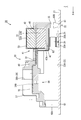
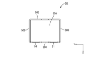
- Sectional drawing which shows the electrical-connection box of Embodiment 1.
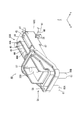
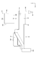
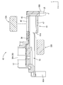
- Longitudinal sectional view of the position passing through the recess of the pedestal in the inductor with substrate The perspective view which shows the base part in which the conductive path was formed
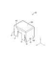
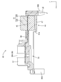
- wearing with a division member with respect to a base part Sectional drawing which shows the state by which the magnetic body core was mounted
- the electrical junction box 10 in which the inductor 30 of the first embodiment is housed is a power supply between a power source such as a battery of a vehicle such as an electric vehicle or a hybrid vehicle and a load composed of an on-vehicle electrical component such as a lamp or a drive motor.
- a power source such as a battery of a vehicle such as an electric vehicle or a hybrid vehicle
- a load composed of an on-vehicle electrical component such as a lamp or a drive motor.
- a DC-DC converter or an inverter for a DC-DC converter or an inverter.
- the electrical connection box 10 includes an inductor 20 with a substrate and a case 11 that accommodates the inductor 20 with a substrate.
- the case 11 is made of synthetic resin or metal, and has a lower case 13 and an upper case 12 that fits into the lower case 13.
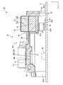
- the substrate-equipped inductor 20 includes a substrate 21, a plurality of electronic components 25 mounted on the substrate 21, and an inductor 30 mounted on the substrate 21.
- the board 21 is a printed board in which an insulating plate made of an insulating material is formed with a pattern 23 made of copper foil or the like by a printed wiring technique.
- the pattern 23 has a ground pattern 23A connected to the ground potential.
- the substrate 21 is only a printed board.
- the present invention is not limited to this.
- a board in which a metal plate material (bus bar) such as copper or copper alloy is superimposed on the printed board may be used.
- a plurality of through holes 22 that continue to the pattern 23 are formed through the substrate 21.
- Each electronic component 25 has a plurality of lead terminals 25 ⁇ / b> A connected to the pattern 23 of the substrate 21.
- the plurality of lead terminals 25A are soldered to the pattern 23 of the substrate 21, and one lead terminal 25A of the electronic component 25 is connected to the ground pattern 23A.
- At least one electronic component 25 mounted on the substrate 21 is disposed in a space below the inductor 30.
- the electronic component 25 it can be set as various electronic components, such as a capacitor, FET (Field
- the inductor 30 includes a magnetic core 31, a conductive path 34 that penetrates the magnetic core 31, a pedestal portion 40 made of an insulating synthetic resin that holds the magnetic core 31 and the conductive path 34, and energization of the conductive path 34. And a shield part 63 that shields the magnetic field generated by.
- the magnetic core 31 is made of a magnetic material such as ferrite, and is configured by facing a pair of divided members 32A and 32B having the same shape. A flat plate-like insertion portion 42 of the pedestal portion 40 is inserted between the pair of divided members 32A and 32B.
- the magnetic core 31 may be fixed by winding a tape from the outside of the pair of divided members 32A and 32B in a state where the pair of divided members 32A and 32B sandwich the insertion portion 42.
- the conductive path 34 is made of a flat metal plate (bus bar) such as copper or copper alloy, and a plurality of board connection terminals 35 bent at one end side to be L-shaped and connected to the conductive path 34 of the board 21. The other end side is bent in a stepped shape, and a through hole 34A through which the shaft portion of the stud bolt 36 is inserted is formed in the heightened step.
- a shaft portion of the stud bolt 36 is a terminal portion 36A that can be connected to a mating terminal TE connected to a terminal portion of an external electric wire.
- the terminal portion 36A is an output terminal that outputs electric power to the outside.
- another terminal portion (not shown) to which electric power is input from the outside is mounted on the substrate 21.
- the head of the stud bolt 36 is welded to the hole edge of the through hole 34 ⁇ / b> A in the conductive path 34.
- the plurality of substrate connection terminals 35 are both rod-shaped, arranged in a line at predetermined intervals, and are inserted into the through holes 22 of the substrate 21 and soldered. Thereby, it is electrically connected to the pattern 23 of the substrate 21.
- the pedestal portion 40 is made of an insulating synthetic resin, and is in close contact with the entire surface of the conductive path 34 other than the upper surface of the terminal portion 36A, and includes a core holding portion 41 that holds the magnetic core 31, and a terminal portion.
- the core holding portion 41 is disposed below the insertion portion 42, the insertion portion 42 inserted between the pair of division members 32A, 32B, the recess 44 into which the end portions of the division members 32A, 32B are fitted.
- a receiving portion 47 for receiving the lower divided member 32B.
- the insertion portion 42 extends in a flat plate shape in the front-rear direction, and is configured such that resin is in close contact with the entire circumference of the conductive path 34.
- the insertion portion 42 is provided with a pair of left and right thin spacer portions 45 that do not overlap the conductive path 34.
- the spacer portion 45 is sandwiched between the divided members 32A and 32B and maintains the space between the divided members 32A and 32B.
- the concave portions 44 are provided on the upper and lower surfaces of the core holding portion 41 and are recessed in a rectangular shape that is long in the front-rear direction.
- An annularly extending rib 44A protrudes from the edge of the recess 44.
- a space 45 is provided between the upper and lower recesses 44.
- the receiving portion 47 is a U-shaped plate shape into which the dividing member 32B can be fitted, and connects the lower side of the left and right side walls of the core holding portion 41. As shown in FIG.
- An inclined surface 47A is formed by cutting out in an inclined shape.
- the upper part of the core holding part 41 is covered with a cover part 50 in a state where the magnetic core 31 is attached to the insertion part 42 of the core holding part 41 as shown in FIG.
- the cover portion 50 connects the rectangular ceiling wall 50A, the side walls 50B and 50D extending downward from both side edges of the ceiling wall 50A, and the side walls 50B and 50D, thereby connecting the ceiling wall 50A.
- a pair of connecting walls 50C and 50E extending downward from the front and rear edges.
- a pair of insertion pieces 51 extend downward in a band shape on the connecting wall 50C. Between each insertion piece 51 and the side walls 50B and 50D, an insertion groove 52 extends in a slit shape in the vertical direction.
- the connecting wall 50E is shortened by notching the lower side.
- the pair of side walls 50 ⁇ / b> B and 50 ⁇ / b> D has a locked portion in which the hole edge is locked to the locking portion 48 projecting from the outer surface of the core holding portion 41 to position the cover portion 50. 53 is penetratingly formed in a rectangular shape.
- the locking part 48 has a lower end protruding in a stepped shape, and a protruding dimension is reduced in an inclined manner toward the upper side.
- the terminal holding part 56 is formed integrally with the core holding part 41, and as shown in FIG. 3, an insulating wall 57 surrounding three sides of the terminal part 36A, and a groove part 58 arranged around the insulating wall 57, Is provided.
- the four support portions 60A to 60D are four columnar legs projecting downward at the four corner positions of the pedestal portion 40 (the bottom surfaces of the core holding portion 41 and the terminal holding portion 56).
- the support portions 60A and 60D on the 56 side are shorter in height than the two support portions 60B and 60C on the core holding portion 41 side, and have a large outer diameter.
- the support surface 61 of the support portions 60A to 60D is placed on the substrate 21, it is formed with a height dimension that can accommodate the electronic component 25 under the core holding portion 41 and the terminal holding portion 56 (on the substrate 21 side).
- the substrate connection terminal 35 is embedded, and the lower end portion is tapered and tapered. As shown in FIG.
- screw holes 61A are formed in the support surface 61 of the support portions 60A and 60D on the terminal holding portion 56 side.
- the substrate 21 may be fixed by screwing into the screw holes 61A of the support portions 60A and 60D with screws (not shown) from the lower side of the substrate 21.
- the shield part 63 is attached to the bottom surface of the receiving part 47 in the pedestal part 40.
- a metal plate material such as aluminum, aluminum alloy, copper, or copper alloy is punched by a press machine and bent. It is made into the box shape which gave.
- the shield part 63 is fitted to the lower surface side of the core holding part 41, and a pair of a base plate part 63 ⁇ / b> A that covers the entire bottom surface of the receiving part 47 and the side walls 50 ⁇ / b> B and 50 ⁇ / b> D of the core holding part 41.
- the shield part 63 can be fixed to the core holding part 41 by, for example, an adhesive.
- the shield part 63 can be fixed using various known fixing means.
- a locking claw (not shown) is provided on one of the shield part 63 and the core holding part 41, and the shield part 63 is shielded.
- the shield 63 may be fixed to the core holding part 41 by providing a locked recess to be locked to the locking claw on the other of the part 63 and the core holding part 41.
- the assembly of the electrical junction box 10 will be described.
- the electronic component 25 is placed on the substrate 21 to which the solder is applied, and the electronic component 25 is soldered to the substrate 21 by, for example, reflow soldering.
- the conductive path 34 and the pedestal portion 40 are integrally formed by insert molding in which a stud bolt 36 is welded to the conductive path 34 formed by a press and the conductive path 34 is arranged in the mold (FIG. 3). .
- one split member 32 ⁇ / b> A is fitted into the upper pair of concave portions 44 from the upper side of the core holding portion 41, and on the inclined surface 47 ⁇ / b> A of the receiving portion 47 from the lower side of the pedestal portion 40.
- the magnetic core 31 is formed by being fitted in the pair of lower recesses 44 while being slid (FIG. 10).
- the cover part 50 is put on the magnetic core 31 (see FIG. 4), and the locked part 53 of the cover part 50 is locked to the locking part 48 of the core holding part 41.
- the inductor 30 is formed by fixing the shield part 63 to the core holding part 41 from below the pedestal part 40 with an adhesive or the like (see FIG. 4).
- the support portions 60A to 60D of the inductor 30 are placed on the substrate 21 while the substrate connection terminals 35 of the inductor 30 are inserted into the through holes 22 of the substrate 21, and the substrate connection terminals 35 are attached to the substrate 21 by, for example, flow soldering. Solder to the through hole 22.
- substrate is formed (FIG. 2).
- the electric connection box 10 is formed by covering the upper case 12 and the lower case 13 on the top and bottom of the inductor 20 with the substrate (FIG. 1).
- the inductor 30 When the inductor 30 is placed on the substrate 21, the magnetic core 31, the conductive path 34 that penetrates the magnetic core 31, the core holding portion 41 that holds the magnetic core 31, and the core holding portion 41.
- a pedestal portion 40 having support portions 60A to 60D that support the electronic component 25 at a height that can accommodate the electronic component 25 on the substrate 21 side, and the magnetic core 31 is provided on the substrate 21 side, and is generated by energization of the conductive path 34.
- a shield part 63 that shields the magnetic field.
- the electronic component 25 when the support portions 60A to 60D of the inductor 30 are placed on the substrate 21, the electronic component 25 can be accommodated between the core holding portion 41 and the substrate 21.
- the space in which the electronic component 25 can be accommodated is increased, the mounting density of the electronic component 25 can be increased, and the size can be reduced.
- the inductor 30 when the inductor 30 is placed on the substrate 21 in this way, the distance between the conductive path 34 of the inductor 30 and the electronic component 25 on the substrate 21 is short, and therefore, when the current is energized, the electrons are transferred from the conductive path 34. There is a concern about the influence of the magnetic field on the component 25.
- the magnetic field generated on the electronic component 25 side by energization of the conductive path 34 is shielded by the shield part 63, the influence on the electronic component 25 by the magnetic field generated by energization of the conductive path 34 can be suppressed. it can. Therefore, it is possible to suppress the influence on the electronic component 25 mounted on the substrate 21 by the magnetic field generated by energization of the conductive path 34 in the inductor 30 while enabling the miniaturization.
- the electroconductive cover part 50 which covers the opposite side to the board
- the terminal portion 36A includes a terminal holding portion 56 that holds the terminal portion 36A.
- the terminal portion 36A includes a terminal portion 36A that is connected to the conductive path 34 and can be connected to an external terminal. In this way, the inductor 30 can suppress the influence on the electronic component 25 mounted on the substrate 21 by the magnetic field generated by energization of the terminal portion 36A while having the function of the terminal block.
- the inductor 20 with substrate is mounted on the substrate 21 having the ground pattern 23A on which the inductor 30 and the pedestal portion 40 are mounted and connected to the ground potential, and the lead terminal connected to the ground pattern 23A.
- an electronic component 25 having 25A is provided. Although there is a concern about the influence on the electronic component 25 connected to the ground pattern 23A due to the influence of the magnetic field from the inductor 30, according to the present embodiment, the influence of the magnetic field is likely to occur due to the connection to the ground pattern 23A. The influence on the electronic component 25 can be suppressed in the configuration.
- Embodiment 2 will be described with reference to FIG.
- a shield portion 72 is provided on the bottom surface of the terminal holding portion 56 in addition to the core holding portion 41.
- the same components as those of the first embodiment are denoted by the same reference numerals and description thereof is omitted.
- the shield portion 72 is provided over the entire bottom surface (lower surface) of the pedestal portion 40 of the inductor 71.
- the shield portion is not limited to this, and may be provided on the outer surface or the upper surface of the pedestal portion 40.
- the shield portion is provided over the entire outer surface (other than the terminal portion 36A) of the pedestal portion 40. It may be.
- an electronic component 26 such as a capacitor, FET, resistor, or coil may be mounted on the substrate 21 below the terminal holding portion 56 on the substrate 21.
- the shield portion 72 is provided over the entire surface of the base portion 40 on the substrate 21 side, the entire conductive path 34 in the inductor 71 is mounted on the substrate 21. The influence on 25 and 26 can be suppressed.
- the technology described in the present specification is not limited to the embodiments described with reference to the above description and the drawings.
- the following embodiments are also included in the technical scope of the technology described in the present specification.
- the shape of the shield part 63 is not limited to the box shape described above, and may be various shapes.
- a flat plate shape that covers only the bottom surface of the core holding portion 41 may be used.
- the shield part 63 is not limited to a metal plate material, and may be a metal foil such as aluminum or copper, or a mesh braided wire. Further, a conductive resin may be used as the shield part 63.
- the pedestal portion 40 is made of synthetic resin, but is not limited thereto.
- the pedestal portion may be made of metal, and the conductive path 34 and the inductor 30 may be insulated by an insulating layer made of an insulating adhesive or the like.
- the direction of the plate surface of the conductive path 34 extending into the pedestal portion 40 may be a direction different from the above embodiment.
- a conductive path having a plate surface in a direction orthogonal to the plate surface of the conductive path 34 may be inserted through the magnetic core.
- the pair of divided members 32A and 32B may be fitted from the left and right directions according to the direction of the plate surface of the conductive path.
- the inductor 30 is formed by insert molding in which the conductive path 34 is arranged in the mold and the resin is injected into the mold, the invention is not limited thereto.
- the inductor may be formed by assembling the conductive path to the pedestal portion.
Landscapes
- Engineering & Computer Science (AREA)
- Power Engineering (AREA)
- Microelectronics & Electronic Packaging (AREA)
- Shielding Devices Or Components To Electric Or Magnetic Fields (AREA)
- Housings And Mounting Of Transformers (AREA)
- Coils Or Transformers For Communication (AREA)
- Regulation Of General Use Transformers (AREA)
- Connection Or Junction Boxes (AREA)
Abstract
Provided is an inductor 30 comprising: a magnetic core 31; a conductive path 34 that passes through the magnetic core 31; a seat part 40 having a core holding part 41 that supports the magnetic core 31, and having support parts 60A-60D that support electronic parts 25 at such a height that the electronic parts 25 can be accommodated at a board 21 side with respect to a core holding part 41 when placed on the board 21; and a shield part 63 that is provided at a board 21 side with respect to the magnetic core 31 and shields against the magnetic field caused by energization of the conductive path 34.
Description
本明細書では、インダクタ、基板付きインダクタ及び電気接続箱に関する技術を開示する。
In this specification, the technology regarding an inductor, an inductor with a substrate, and an electrical junction box is disclosed.
従来、基板にインダクタ部品が実装される技術が知られている。特許文献1は、実装基板に実装されるインダクタ部品である第1の電子部品には凹部が形成されている。第2の電子部品は、第1の電子部品の凹部において実装基板に実装されている。これにより、第2の電子部品の実装面積分だけ実装面積を減少させ、実装基板を小さくして小型化されている。
Conventionally, a technique in which an inductor component is mounted on a substrate is known. In Patent Document 1, a recess is formed in a first electronic component that is an inductor component mounted on a mounting board. The second electronic component is mounted on the mounting substrate in the recess of the first electronic component. As a result, the mounting area is reduced by the mounting area of the second electronic component, and the mounting substrate is reduced in size.
ところで、上記構成では、インダクタ部品の凹部に第2の電子部品を配することで小型化が可能になるものの、インダクタ部品から生じる磁界により第2の電子部品に影響が生じることが懸念される。
By the way, in the above configuration, the second electronic component can be reduced in size by arranging the second electronic component in the concave portion of the inductor component, but there is a concern that the second electronic component may be affected by the magnetic field generated from the inductor component.
本明細書に記載された技術は、上記のような事情に基づいて完成されたものであって、小型化を可能としつつ、インダクタ内の導電路の通電で生じる磁界による基板に実装される電子部品への影響を抑制することが可能なインダクタ、基板付きインダクタ及び電気接続箱を提供することを目的とする。
The technology described in the present specification has been completed based on the above-described circumstances, and can be reduced in size while being mounted on a substrate by a magnetic field generated by energization of a conductive path in an inductor. An object of the present invention is to provide an inductor, an inductor with a substrate, and an electrical junction box that can suppress the influence on components.
本明細書に記載されたインダクタは、磁性体コアと、前記磁性体コアを貫通する導電路と、前記磁性体コアを保持するコア保持部と基板に載置された際に前記コア保持部に対して前記基板側に電子部品を収容可能な高さで支持する支持部とを有する台座部と、前記磁性体コアに対して前記基板側に設けられ、前記導電路の通電により生じる磁界を遮蔽するシールド部と、を備える。
本構成によれば、インダクタの支持部が基板に載置された際に、コイル保持部と基板との間に電子部品を収容することが可能になるため、基板上における電子部品を収容可能なスペースが多くなって電子部品の実装密度を高めることができ、小型化が可能になる。ここで、このように基板にインダクタを載置した場合には、インダクタの導電路と基板上の電子部品との間の距離が近くなるため、導電路から電子部品への磁界の影響が懸念される。本構成によれば、導電路の通電により電子部品側に生じる磁界がシールド部により遮蔽されるため、導電路の通電で生じる磁界による電子部品への影響を抑制することができる。よって、小型化を可能としつつ、インダクタ内の導電路の通電で生じる磁界による基板に実装される電子部品への影響を抑制することが可能となる。 The inductor described in this specification includes a magnetic core, a conductive path that penetrates the magnetic core, a core holding portion that holds the magnetic core, and a core holding portion that is placed on the substrate. On the other hand, a pedestal portion having a support portion that supports the electronic component at a height that can accommodate an electronic component on the substrate side, and provided on the substrate side with respect to the magnetic core, shields a magnetic field generated by energization of the conductive path. And a shield part to be provided.
According to this configuration, when the support portion of the inductor is placed on the substrate, the electronic component can be accommodated between the coil holding portion and the substrate, so that the electronic component on the substrate can be accommodated. The space increases, the mounting density of electronic components can be increased, and miniaturization becomes possible. Here, when the inductor is placed on the board in this way, the distance between the conductive path of the inductor and the electronic component on the board becomes short, and there is a concern about the influence of the magnetic field from the conductive path to the electronic component. The According to this configuration, since the magnetic field generated on the electronic component side by energization of the conductive path is shielded by the shield portion, the influence on the electronic component by the magnetic field generated by energization of the conductive path can be suppressed. Accordingly, it is possible to reduce the size of the electronic component mounted on the substrate due to the magnetic field generated by energization of the conductive path in the inductor.
本明細書に記載された技術の実施態様としては以下の態様が好ましい。
前記磁性体コアにおける前記基板側とは反対側を覆う導電性のカバー部を備える。
このようにすれば、導電性のカバー部により磁性体コアに対して基板側とは反対側に生じる磁界の外部への影響を抑制することができる。 The following embodiments are preferable as the embodiments of the technology described in this specification.
A conductive cover portion is provided that covers the opposite side of the magnetic core from the substrate side.
If it does in this way, the influence on the exterior of the magnetic field which arises on the opposite side to a substrate side to a magnetic body core with a conductive cover part can be controlled.
前記シールド部は、前記台座部における前記基板側の面の全体に亘って設けられている。
このようにすれば、インダクタ内の導電路の全体について基板に実装される電子部品への影響を抑制することが可能となる。 The shield part is provided over the entire surface of the base part on the substrate side.
In this way, it is possible to suppress the influence of the entire conductive path in the inductor on the electronic component mounted on the board.
このようにすれば、インダクタ内の導電路の全体について基板に実装される電子部品への影響を抑制することが可能となる。 The shield part is provided over the entire surface of the base part on the substrate side.
In this way, it is possible to suppress the influence of the entire conductive path in the inductor on the electronic component mounted on the board.
前記導電路に接続され、外部の端子と接続可能な端子部を備え、前記台座部は、前記端子部を保持する端子保持部を備える。
このようにすれば、インダクタは、端子台の機能を有しつつ、端子部の通電により生じる磁界による基板側への影響を抑制することが可能となる。 A terminal portion connected to the conductive path and connectable to an external terminal is provided, and the pedestal portion includes a terminal holding portion that holds the terminal portion.
In this way, the inductor can suppress the influence of the magnetic field generated by energization of the terminal portion on the substrate side while having the function of the terminal block.
前記インダクタと、前記台座部が載置され、グランド電位に接続されたグランドパターンを有する基板と、前記基板に実装され、前記グランドパターンに接続される端子を有する前記電子部品と、を備える基板付きインダクタとする。
インダクタからの磁界の影響により基板のグランドパターンに接続される電子部品への影響が懸念されるが、本構成によれば、そのようなグランドパターンに接続されて磁界の影響が生じやすい構成において電子部品への影響を抑制することができる。 With the substrate comprising: the inductor; a substrate on which the pedestal portion is mounted and having a ground pattern connected to a ground potential; and the electronic component mounted on the substrate and having a terminal connected to the ground pattern An inductor is used.
Although there is a concern about the influence on the electronic components connected to the ground pattern of the board due to the influence of the magnetic field from the inductor, according to this configuration, the electronic circuit is easily connected to such a ground pattern and the magnetic field is likely to be affected. The influence on components can be suppressed.
前記インダクタと、前記基板と、前記電子部品と、前記インダクタ、前記基板及び前記電子部品を収容するケースとを備える電気接続箱とする。
Suppose that the electric junction box includes the inductor, the substrate, the electronic component, and a case that accommodates the inductor, the substrate, and the electronic component.
本明細書に記載された技術によれば、小型化を可能としつつ、導電路の通電で生じる磁界による基板に実装される電子部品への影響を抑制することが可能となる。
According to the technique described in the present specification, it is possible to reduce the size of the electronic component mounted on the substrate due to the magnetic field generated by energization of the conductive path while enabling downsizing.
実施形態1について図1~図11を参照しつつ説明する。
実施形態1のインダクタ30が収容される電気接続箱10は、例えば電気自動車やハイブリット自動車等の車両のバッテリ等の電源とランプ等の車載電装品や駆動モータ等からなる負荷との間の電力供給経路に配され、例えばDC-DCコンバータやインバータ等に用いることができる。以下では、図3のX方向を前方、Y方向を右方、Z方向を上方として説明する。 The first embodiment will be described with reference to FIGS.
Theelectrical junction box 10 in which the inductor 30 of the first embodiment is housed is a power supply between a power source such as a battery of a vehicle such as an electric vehicle or a hybrid vehicle and a load composed of an on-vehicle electrical component such as a lamp or a drive motor. For example, it can be used for a DC-DC converter or an inverter. In the following description, it is assumed that the X direction in FIG. 3 is the front, the Y direction is the right, and the Z direction is the upper.
実施形態1のインダクタ30が収容される電気接続箱10は、例えば電気自動車やハイブリット自動車等の車両のバッテリ等の電源とランプ等の車載電装品や駆動モータ等からなる負荷との間の電力供給経路に配され、例えばDC-DCコンバータやインバータ等に用いることができる。以下では、図3のX方向を前方、Y方向を右方、Z方向を上方として説明する。 The first embodiment will be described with reference to FIGS.
The
電気接続箱10は、図1に示すように、基板付きインダクタ20と、基板付きインダクタ20を収容するケース11とを備える。ケース11は、合成樹脂製又は金属製であって、ロアケース13とこのロアケース13に嵌合するアッパケース12とを有する。
As shown in FIG. 1, the electrical connection box 10 includes an inductor 20 with a substrate and a case 11 that accommodates the inductor 20 with a substrate. The case 11 is made of synthetic resin or metal, and has a lower case 13 and an upper case 12 that fits into the lower case 13.
基板付きインダクタ20は、図2に示すように、基板21と、基板21に実装される複数の電子部品25と、基板21に実装されるインダクタ30とを備える。基板21は、絶縁材料からなる絶縁板に銅箔等からなるパターン23がプリント配線技術により形成されたプリント基板とされている。パターン23は、グランド電位に接続されたグランドパターン23Aを有する。なお、本実施形態では、基板21は、プリント基板のみとしたが、これに限られず、例えば、プリント基板に銅、銅合金等の金属板材(バスバ―)が重ねられた基板を用いてもよい。基板21には、パターン23に連なる複数のスルーホール22が貫通形成されている。
As shown in FIG. 2, the substrate-equipped inductor 20 includes a substrate 21, a plurality of electronic components 25 mounted on the substrate 21, and an inductor 30 mounted on the substrate 21. The board 21 is a printed board in which an insulating plate made of an insulating material is formed with a pattern 23 made of copper foil or the like by a printed wiring technique. The pattern 23 has a ground pattern 23A connected to the ground potential. In the present embodiment, the substrate 21 is only a printed board. However, the present invention is not limited to this. For example, a board in which a metal plate material (bus bar) such as copper or copper alloy is superimposed on the printed board may be used. . A plurality of through holes 22 that continue to the pattern 23 are formed through the substrate 21.
各電子部品25は、基板21のパターン23に接続される複数のリード端子25Aを有する。複数のリード端子25Aは、基板21のパターン23に半田付けされており、電子部品25の一つのリード端子25Aは、グランドパターン23Aに接続されている。基板21に実装される少なくとも一つの電子部品25は、インダクタ30の下側のスペースに配置されている。電子部品25としては、例えば、コンデンサ、FET(Field Effect Transistor)、抵抗、コイル等の種々の電子部品とすることができる。
Each electronic component 25 has a plurality of lead terminals 25 </ b> A connected to the pattern 23 of the substrate 21. The plurality of lead terminals 25A are soldered to the pattern 23 of the substrate 21, and one lead terminal 25A of the electronic component 25 is connected to the ground pattern 23A. At least one electronic component 25 mounted on the substrate 21 is disposed in a space below the inductor 30. As the electronic component 25, it can be set as various electronic components, such as a capacitor, FET (Field | Effect | Transfector), resistance, a coil, for example.
インダクタ30は、磁性体コア31と、磁性体コア31を貫通する導電路34と、磁性体コア31及び導電路34を保持する絶縁性の合成樹脂からなる台座部40と、導電路34の通電により生じる磁界を遮蔽するシールド部63とを備える。
The inductor 30 includes a magnetic core 31, a conductive path 34 that penetrates the magnetic core 31, a pedestal portion 40 made of an insulating synthetic resin that holds the magnetic core 31 and the conductive path 34, and energization of the conductive path 34. And a shield part 63 that shields the magnetic field generated by.
磁性体コア31は、フェライト等の磁性体からなり、同一形状の一対の分割部材32A,32Bを対向させて構成されている。一対の分割部材32A,32Bの間には、台座部40の平板状の挿通部42が挿通されている。なお、磁性体コア31は、一対の分割部材32A,32Bが挿通部42を挟んだ状態で一対の分割部材32A,32Bの外側からテープを巻き付けて固定してもよい。
The magnetic core 31 is made of a magnetic material such as ferrite, and is configured by facing a pair of divided members 32A and 32B having the same shape. A flat plate-like insertion portion 42 of the pedestal portion 40 is inserted between the pair of divided members 32A and 32B. The magnetic core 31 may be fixed by winding a tape from the outside of the pair of divided members 32A and 32B in a state where the pair of divided members 32A and 32B sandwich the insertion portion 42.
導電路34は、銅、銅合金等の平板状の金属板材(バスバ―)からなり、一端側はL字状に屈曲されて基板21の導電路34に接続される複数の基板接続端子35が形成され、他端側は、段差状に屈曲され、一段高くされた部分にスタッドボルト36の軸部が挿通される貫通孔34Aが形成されている。スタッドボルト36の軸部は、外部の電線の端末部に接続される相手側端子TEに接続可能な端子部36Aとされている。端子部36Aは、外部に電力を出力する出力端子とされ、基板21上には、端子部36Aとは異なり、外部から電力が入力される図示しない他の端子部が実装されている。スタッドボルト36の頭部は導電路34における貫通孔34Aの孔縁部に溶接されている。
The conductive path 34 is made of a flat metal plate (bus bar) such as copper or copper alloy, and a plurality of board connection terminals 35 bent at one end side to be L-shaped and connected to the conductive path 34 of the board 21. The other end side is bent in a stepped shape, and a through hole 34A through which the shaft portion of the stud bolt 36 is inserted is formed in the heightened step. A shaft portion of the stud bolt 36 is a terminal portion 36A that can be connected to a mating terminal TE connected to a terminal portion of an external electric wire. The terminal portion 36A is an output terminal that outputs electric power to the outside. Unlike the terminal portion 36A, another terminal portion (not shown) to which electric power is input from the outside is mounted on the substrate 21. The head of the stud bolt 36 is welded to the hole edge of the through hole 34 </ b> A in the conductive path 34.
複数の基板接続端子35は、図3に示すように、共に棒状であって、互いに所定間隔を空けて一列に並んで配されており、基板21のスルーホール22に挿通されて半田付けされることにより基板21のパターン23に電気的に接続される。
As shown in FIG. 3, the plurality of substrate connection terminals 35 are both rod-shaped, arranged in a line at predetermined intervals, and are inserted into the through holes 22 of the substrate 21 and soldered. Thereby, it is electrically connected to the pattern 23 of the substrate 21.
台座部40は、絶縁性の合成樹脂製であって、端子部36Aの上面以外の導電路34の全面に亘って密着しており、磁性体コア31を保持するコア保持部41と、端子部36Aを保持する端子保持部56と、コア保持部41及び端子保持部56を支持する支持部60A~60Dとを備える。コア保持部41は、一対の分割部材32A,32Bの間に挿通される挿通部42と、分割部材32A,32Bの端部が嵌め入れられる凹部44と、挿通部42の下側に配されて下側の分割部材32Bを受ける受け部47とを有する。
The pedestal portion 40 is made of an insulating synthetic resin, and is in close contact with the entire surface of the conductive path 34 other than the upper surface of the terminal portion 36A, and includes a core holding portion 41 that holds the magnetic core 31, and a terminal portion. A terminal holding part 56 for holding 36A, and support parts 60A to 60D for supporting the core holding part 41 and the terminal holding part 56. The core holding portion 41 is disposed below the insertion portion 42, the insertion portion 42 inserted between the pair of division members 32A, 32B, the recess 44 into which the end portions of the division members 32A, 32B are fitted. And a receiving portion 47 for receiving the lower divided member 32B.
挿通部42は、前後方向に平板状に延びており、導電路34の全周に樹脂が密着されて構成されている。挿通部42には、導電路34に重ならない薄肉のスペーサ部45が左右一対設けられている。スペーサ部45は、分割部材32A,32Bの間に挟まれて分割部材32A,32Bの間の間隔を保持する。
The insertion portion 42 extends in a flat plate shape in the front-rear direction, and is configured such that resin is in close contact with the entire circumference of the conductive path 34. The insertion portion 42 is provided with a pair of left and right thin spacer portions 45 that do not overlap the conductive path 34. The spacer portion 45 is sandwiched between the divided members 32A and 32B and maintains the space between the divided members 32A and 32B.
凹部44は、コア保持部41の上下両面に設けられ、前後方向に長い長方形状に凹んでいる。凹部44の縁部は、環状に延びるリブ44Aが突出している。上下の凹部44の間は、スペーサ部45とされている。受け部47は、分割部材32Bを嵌め入れ可能なU字の板状であって、コア保持部41の左右の側壁の下側を連結しており、図2に示すように、先端側の内面が傾斜状に切り欠かれた傾斜面47Aが形成されている。
The concave portions 44 are provided on the upper and lower surfaces of the core holding portion 41 and are recessed in a rectangular shape that is long in the front-rear direction. An annularly extending rib 44A protrudes from the edge of the recess 44. A space 45 is provided between the upper and lower recesses 44. The receiving portion 47 is a U-shaped plate shape into which the dividing member 32B can be fitted, and connects the lower side of the left and right side walls of the core holding portion 41. As shown in FIG. An inclined surface 47A is formed by cutting out in an inclined shape.
コア保持部41の上方は、図2に示すように、コア保持部41の挿通部42に磁性体コア31を装着した状態でカバー部50により覆われる。カバー部50は、図6~図8に示すように、長方形状の天井壁50Aと、天井壁50Aの両側縁から下方に延びる側壁50B,50Dと、側壁50B,50Dを連結し、天井壁50Aの前後の縁から下方に延びる一対の連結壁50C,50Eとを有する。連結壁50Cには、一対の挿通片51が下方に帯状に延びている。各挿通片51と側壁50B,50Dとの間には、挿通溝52が上下方向にスリット状に延びている。連結壁50Eは、下方側が切り欠かれて短くされている。一対の側壁50B,50Dには、図4に示すように、コア保持部41の外側面に突設された係止部48に孔縁が係止してカバー部50を位置決めする被係止部53が長方形状に貫通形成されている。係止部48は、下端が段差状に突出し、上方側に向けて傾斜状に突出寸法が小さくされている。
The upper part of the core holding part 41 is covered with a cover part 50 in a state where the magnetic core 31 is attached to the insertion part 42 of the core holding part 41 as shown in FIG. As shown in FIGS. 6 to 8, the cover portion 50 connects the rectangular ceiling wall 50A, the side walls 50B and 50D extending downward from both side edges of the ceiling wall 50A, and the side walls 50B and 50D, thereby connecting the ceiling wall 50A. And a pair of connecting walls 50C and 50E extending downward from the front and rear edges. A pair of insertion pieces 51 extend downward in a band shape on the connecting wall 50C. Between each insertion piece 51 and the side walls 50B and 50D, an insertion groove 52 extends in a slit shape in the vertical direction. The connecting wall 50E is shortened by notching the lower side. As shown in FIG. 4, the pair of side walls 50 </ b> B and 50 </ b> D has a locked portion in which the hole edge is locked to the locking portion 48 projecting from the outer surface of the core holding portion 41 to position the cover portion 50. 53 is penetratingly formed in a rectangular shape. The locking part 48 has a lower end protruding in a stepped shape, and a protruding dimension is reduced in an inclined manner toward the upper side.
端子保持部56は、コア保持部41と一体に形成されており、図3に示すように、端子部36Aの三方を包囲する絶縁壁57と、絶縁壁57の周りに配される溝部58とを備える。
The terminal holding part 56 is formed integrally with the core holding part 41, and as shown in FIG. 3, an insulating wall 57 surrounding three sides of the terminal part 36A, and a groove part 58 arranged around the insulating wall 57, Is provided.
4つの支持部60A~60Dは、台座部40(コア保持部41及び端子保持部56の底面側)の四隅の位置に下方に突設された円柱状の4本の脚であり、端子保持部56側の支持部60A,60Dは、コア保持部41側の2つの支持部60B,60Cよりも高さ寸法が短く、外径が太径とされている。支持部60A~60Dの支持面61が基板21に載置された際にコア保持部41及び端子保持部56の下側(基板21側)に電子部品25を収容可能となる高さ寸法で形成されている。コア保持部41側の2つの支持部60B,60Cは、基板接続端子35が埋設されており、下端部がテーパ状に先細の形状とされている。端子保持部56側の支持部60A,60Dの支持面61には、図5に示すように、ネジ穴61Aが形成されている。基板21の下側から図示しないネジにより基板21を支持部60A,60Dのネジ穴61Aにネジ留めして固定してもよい。
The four support portions 60A to 60D are four columnar legs projecting downward at the four corner positions of the pedestal portion 40 (the bottom surfaces of the core holding portion 41 and the terminal holding portion 56). The support portions 60A and 60D on the 56 side are shorter in height than the two support portions 60B and 60C on the core holding portion 41 side, and have a large outer diameter. When the support surface 61 of the support portions 60A to 60D is placed on the substrate 21, it is formed with a height dimension that can accommodate the electronic component 25 under the core holding portion 41 and the terminal holding portion 56 (on the substrate 21 side). Has been. In the two support portions 60B and 60C on the core holding portion 41 side, the substrate connection terminal 35 is embedded, and the lower end portion is tapered and tapered. As shown in FIG. 5, screw holes 61A are formed in the support surface 61 of the support portions 60A and 60D on the terminal holding portion 56 side. The substrate 21 may be fixed by screwing into the screw holes 61A of the support portions 60A and 60D with screws (not shown) from the lower side of the substrate 21.
シールド部63は、図2に示すように、台座部40における受け部47の底面に取付けられており、例えば、アルミニウム、アルミニウム合金、銅、銅合金等の金属板材をプレス機により打ち抜いて曲げ加工を施した箱形状とされている。シールド部63は、図5に示すように、コア保持部41の下面側に外嵌し、受け部47の底面の全体を覆う底板部63Aと、コア保持部41の側壁50B,50Dを覆う一対の側壁部63B,63Dと、一対の側壁部63B,63Dを連結し、底板部63Aの前縁から下方に延びる連結壁部63Eとを有する。
As shown in FIG. 2, the shield part 63 is attached to the bottom surface of the receiving part 47 in the pedestal part 40. For example, a metal plate material such as aluminum, aluminum alloy, copper, or copper alloy is punched by a press machine and bent. It is made into the box shape which gave. As shown in FIG. 5, the shield part 63 is fitted to the lower surface side of the core holding part 41, and a pair of a base plate part 63 </ b> A that covers the entire bottom surface of the receiving part 47 and the side walls 50 </ b> B and 50 </ b> D of the core holding part 41. Side wall portions 63B and 63D, and a pair of side wall portions 63B and 63D, and a connecting wall portion 63E extending downward from the front edge of the bottom plate portion 63A.
シールド部63のコア保持部41への固定は、例えば、接着剤により固定することができる。なお、これに限られず、シールド部63の固定は、種々の公知の固定手段を用いることができ、例えば、シールド部63及びコア保持部41の一方に係止爪(図示しない)を設け、シールド部63及びコア保持部41の他方に係止爪に係止する被係止凹部を設けてシールド部63をコア保持部41に固定するようにしてもよい。
The shield part 63 can be fixed to the core holding part 41 by, for example, an adhesive. The shield part 63 can be fixed using various known fixing means. For example, a locking claw (not shown) is provided on one of the shield part 63 and the core holding part 41, and the shield part 63 is shielded. The shield 63 may be fixed to the core holding part 41 by providing a locked recess to be locked to the locking claw on the other of the part 63 and the core holding part 41.
電気接続箱10の組み付けについて説明する。
半田を塗布した基板21に電子部品25を載置し、例えばリフロー半田付けにより、基板21に電子部品25を半田付けする。また、プレス機により形成した導電路34にスタッドボルト36を溶接し、金型内に導電路34を配したインサート成形により、導電路34と台座部40とを一体的に形成する(図3)。 The assembly of theelectrical junction box 10 will be described.
Theelectronic component 25 is placed on the substrate 21 to which the solder is applied, and the electronic component 25 is soldered to the substrate 21 by, for example, reflow soldering. Further, the conductive path 34 and the pedestal portion 40 are integrally formed by insert molding in which a stud bolt 36 is welded to the conductive path 34 formed by a press and the conductive path 34 is arranged in the mold (FIG. 3). .
半田を塗布した基板21に電子部品25を載置し、例えばリフロー半田付けにより、基板21に電子部品25を半田付けする。また、プレス機により形成した導電路34にスタッドボルト36を溶接し、金型内に導電路34を配したインサート成形により、導電路34と台座部40とを一体的に形成する(図3)。 The assembly of the
The
次に、図9に示すように、コア保持部41の上方側から一方の分割部材32Aを上側の一対の凹部44に嵌め込み、台座部40の下側から受け部47の傾斜面47Aの上にスライドさせつつ、下側の一対の凹部44に嵌め込むことで磁性体コア31が形成される(図10)。次に、磁性体コア31の上にカバー部50を被せ(図4参照)、カバー部50の被係止部53をコア保持部41の係止部48に係止させる。
Next, as shown in FIG. 9, one split member 32 </ b> A is fitted into the upper pair of concave portions 44 from the upper side of the core holding portion 41, and on the inclined surface 47 </ b> A of the receiving portion 47 from the lower side of the pedestal portion 40. The magnetic core 31 is formed by being fitted in the pair of lower recesses 44 while being slid (FIG. 10). Next, the cover part 50 is put on the magnetic core 31 (see FIG. 4), and the locked part 53 of the cover part 50 is locked to the locking part 48 of the core holding part 41.
次に、シールド部63を台座部40の下側から接着剤等でコア保持部41に固定することにより(図4参照)、インダクタ30が形成される。次に、インダクタ30の基板接続端子35を基板21のスルーホール22に挿通しつつインダクタ30の支持部60A~60Dを基板21に載置し、例えばフロー半田付けにより、基板接続端子35を基板21のスルーホール22に半田付けする。これにより、基板付きインダクタ20が形成される(図2)。基板付きインダクタ20の上下にアッパケース12及びロアケース13を被せることにより、電気接続箱10が形成される(図1)。
Next, the inductor 30 is formed by fixing the shield part 63 to the core holding part 41 from below the pedestal part 40 with an adhesive or the like (see FIG. 4). Next, the support portions 60A to 60D of the inductor 30 are placed on the substrate 21 while the substrate connection terminals 35 of the inductor 30 are inserted into the through holes 22 of the substrate 21, and the substrate connection terminals 35 are attached to the substrate 21 by, for example, flow soldering. Solder to the through hole 22. Thereby, the inductor 20 with a board | substrate is formed (FIG. 2). The electric connection box 10 is formed by covering the upper case 12 and the lower case 13 on the top and bottom of the inductor 20 with the substrate (FIG. 1).
本実施形態の作用、効果について説明する。
インダクタ30は、磁性体コア31と、磁性体コア31を貫通する導電路34と、磁性体コア31を保持するコア保持部41と基板21に載置された際にコア保持部41に対して基板21側に電子部品25を収容可能な高さで支持する支持部60A~60Dとを有する台座部40と、磁性体コア31に対して基板21側に設けられ、導電路34の通電により生じる磁界を遮蔽するシールド部63と、を備える。 The operation and effect of this embodiment will be described.
When theinductor 30 is placed on the substrate 21, the magnetic core 31, the conductive path 34 that penetrates the magnetic core 31, the core holding portion 41 that holds the magnetic core 31, and the core holding portion 41. A pedestal portion 40 having support portions 60A to 60D that support the electronic component 25 at a height that can accommodate the electronic component 25 on the substrate 21 side, and the magnetic core 31 is provided on the substrate 21 side, and is generated by energization of the conductive path 34. And a shield part 63 that shields the magnetic field.
インダクタ30は、磁性体コア31と、磁性体コア31を貫通する導電路34と、磁性体コア31を保持するコア保持部41と基板21に載置された際にコア保持部41に対して基板21側に電子部品25を収容可能な高さで支持する支持部60A~60Dとを有する台座部40と、磁性体コア31に対して基板21側に設けられ、導電路34の通電により生じる磁界を遮蔽するシールド部63と、を備える。 The operation and effect of this embodiment will be described.
When the
本実施形態によれば、インダクタ30の支持部60A~60Dが基板21に載置された際に、コア保持部41と基板21との間に電子部品25を収容することができるため、基板21上における電子部品25を収容可能なスペースが多くなって電子部品25の実装密度を高めることができ、小型化が可能になる。ここで、このように基板21にインダクタ30を載置した場合には、インダクタ30の導電路34と基板21上の電子部品25との間の距離が近くなるため、通電時に導電路34から電子部品25への磁界の影響が懸念される。本実施形態によれば、導電路34の通電により電子部品25側に生じる磁界がシールド部63により遮蔽されるため、導電路34の通電で生じる磁界による電子部品25への影響を抑制することができる。よって、小型化を可能としつつ、インダクタ30内の導電路34の通電で生じる磁界による基板21に実装される電子部品25への影響を抑制することが可能となる。
According to the present embodiment, when the support portions 60A to 60D of the inductor 30 are placed on the substrate 21, the electronic component 25 can be accommodated between the core holding portion 41 and the substrate 21. The space in which the electronic component 25 can be accommodated is increased, the mounting density of the electronic component 25 can be increased, and the size can be reduced. Here, when the inductor 30 is placed on the substrate 21 in this way, the distance between the conductive path 34 of the inductor 30 and the electronic component 25 on the substrate 21 is short, and therefore, when the current is energized, the electrons are transferred from the conductive path 34. There is a concern about the influence of the magnetic field on the component 25. According to the present embodiment, since the magnetic field generated on the electronic component 25 side by energization of the conductive path 34 is shielded by the shield part 63, the influence on the electronic component 25 by the magnetic field generated by energization of the conductive path 34 can be suppressed. it can. Therefore, it is possible to suppress the influence on the electronic component 25 mounted on the substrate 21 by the magnetic field generated by energization of the conductive path 34 in the inductor 30 while enabling the miniaturization.
また、磁性体コア31における基板21側とは反対側を覆う導電性のカバー部50を備える。
このようにすれば、導電性のカバー部50により磁性体コア31に対して基板21側とは反対側に生じる磁界の外部への影響を抑制することができる。 Moreover, the electroconductive coverpart 50 which covers the opposite side to the board | substrate 21 side in the magnetic body core 31 is provided.
In this way, the influence of the magnetic field generated on the side opposite to thesubstrate 21 side with respect to the magnetic core 31 by the conductive cover 50 can be suppressed.
このようにすれば、導電性のカバー部50により磁性体コア31に対して基板21側とは反対側に生じる磁界の外部への影響を抑制することができる。 Moreover, the electroconductive cover
In this way, the influence of the magnetic field generated on the side opposite to the
また、導電路34に接続され、外部の端子と接続可能な端子部36Aを備え、台座部40は、端子部36Aを保持する端子保持部56を備える。
このようにすれば、インダクタ30は、端子台の機能を有しつつ、端子部36Aの通電により生じる磁界による基板21に実装される電子部品25への影響を抑制することが可能となる。 Theterminal portion 36A includes a terminal holding portion 56 that holds the terminal portion 36A. The terminal portion 36A includes a terminal portion 36A that is connected to the conductive path 34 and can be connected to an external terminal.
In this way, theinductor 30 can suppress the influence on the electronic component 25 mounted on the substrate 21 by the magnetic field generated by energization of the terminal portion 36A while having the function of the terminal block.
このようにすれば、インダクタ30は、端子台の機能を有しつつ、端子部36Aの通電により生じる磁界による基板21に実装される電子部品25への影響を抑制することが可能となる。 The
In this way, the
また、基板付きインダクタ20は、インダクタ30と、台座部40が載置され、グランド電位に接続されたグランドパターン23Aを有する基板21と、基板21に実装され、グランドパターン23Aに接続されるリード端子25Aを有する電子部品25と、を備える。
インダクタ30からの磁界の影響によりグランドパターン23Aに接続される電子部品25への影響が懸念されるが、本実施形態によれば、そのようなグランドパターン23Aに接続されて磁界の影響が生じやすい構成において電子部品25への影響を抑制することができる。 In addition, theinductor 20 with substrate is mounted on the substrate 21 having the ground pattern 23A on which the inductor 30 and the pedestal portion 40 are mounted and connected to the ground potential, and the lead terminal connected to the ground pattern 23A. And an electronic component 25 having 25A.
Although there is a concern about the influence on theelectronic component 25 connected to the ground pattern 23A due to the influence of the magnetic field from the inductor 30, according to the present embodiment, the influence of the magnetic field is likely to occur due to the connection to the ground pattern 23A. The influence on the electronic component 25 can be suppressed in the configuration.
インダクタ30からの磁界の影響によりグランドパターン23Aに接続される電子部品25への影響が懸念されるが、本実施形態によれば、そのようなグランドパターン23Aに接続されて磁界の影響が生じやすい構成において電子部品25への影響を抑制することができる。 In addition, the
Although there is a concern about the influence on the
<実施形態2>
次に、実施形態2について図12を参照しつつ説明する。実施形態2の基板付きインダクタ70は、コア保持部41に加えて端子保持部56の底面にシールド部72を設けたものである。以下では、実施形態1と同一の構成については同一の符号を付して説明を省略する。 <Embodiment 2>
Next, Embodiment 2 will be described with reference to FIG. In theinductor 70 with a substrate of the second embodiment, a shield portion 72 is provided on the bottom surface of the terminal holding portion 56 in addition to the core holding portion 41. In the following, the same components as those of the first embodiment are denoted by the same reference numerals and description thereof is omitted.
次に、実施形態2について図12を参照しつつ説明する。実施形態2の基板付きインダクタ70は、コア保持部41に加えて端子保持部56の底面にシールド部72を設けたものである。以下では、実施形態1と同一の構成については同一の符号を付して説明を省略する。 <Embodiment 2>
Next, Embodiment 2 will be described with reference to FIG. In the
シールド部72は、インダクタ71の台座部40の底面(下面)の全体に亘って設けられている。なお、シールド部はこれに限られず、台座部40の外側面や上面に設けるようにしてもよく、例えば、台座部40の(端子部36A以外の)外面の全面に亘ってシールド部を設けるようにしてもよい。また、基板21上における端子保持部56の下側の基板21にコンデンサ、FET、抵抗、コイル等の電子部品26を実装してもよい。
The shield portion 72 is provided over the entire bottom surface (lower surface) of the pedestal portion 40 of the inductor 71. The shield portion is not limited to this, and may be provided on the outer surface or the upper surface of the pedestal portion 40. For example, the shield portion is provided over the entire outer surface (other than the terminal portion 36A) of the pedestal portion 40. It may be. In addition, an electronic component 26 such as a capacitor, FET, resistor, or coil may be mounted on the substrate 21 below the terminal holding portion 56 on the substrate 21.
実施形態2によれば、シールド部72は、台座部40における基板21側の面の全体に亘って設けられているため、インダクタ71内の導電路34の全体について基板21に実装される電子部品25,26への影響を抑制することが可能となる。
According to the second embodiment, since the shield portion 72 is provided over the entire surface of the base portion 40 on the substrate 21 side, the entire conductive path 34 in the inductor 71 is mounted on the substrate 21. The influence on 25 and 26 can be suppressed.
<他の実施形態>
本明細書に記載された技術は上記記述及び図面によって説明した実施形態に限定されるものではなく、例えば次のような実施形態も本明細書に記載された技術の技術的範囲に含まれる。
(1)シールド部63の形状は上記した箱形状に限られず、種々の形状とすることができる。例えば、コア保持部41の底面のみを覆う平板状としてもよい。また、シールド部63は、金属板材に限られず、アルミニウム、銅等の金属箔としたり、メッシュ状の編組線を用いてもよい。また、シールド部63として導電性樹脂を用いてもよい。 <Other embodiments>
The technology described in the present specification is not limited to the embodiments described with reference to the above description and the drawings. For example, the following embodiments are also included in the technical scope of the technology described in the present specification.
(1) The shape of theshield part 63 is not limited to the box shape described above, and may be various shapes. For example, a flat plate shape that covers only the bottom surface of the core holding portion 41 may be used. The shield part 63 is not limited to a metal plate material, and may be a metal foil such as aluminum or copper, or a mesh braided wire. Further, a conductive resin may be used as the shield part 63.
本明細書に記載された技術は上記記述及び図面によって説明した実施形態に限定されるものではなく、例えば次のような実施形態も本明細書に記載された技術の技術的範囲に含まれる。
(1)シールド部63の形状は上記した箱形状に限られず、種々の形状とすることができる。例えば、コア保持部41の底面のみを覆う平板状としてもよい。また、シールド部63は、金属板材に限られず、アルミニウム、銅等の金属箔としたり、メッシュ状の編組線を用いてもよい。また、シールド部63として導電性樹脂を用いてもよい。 <Other embodiments>
The technology described in the present specification is not limited to the embodiments described with reference to the above description and the drawings. For example, the following embodiments are also included in the technical scope of the technology described in the present specification.
(1) The shape of the
(2)台座部40は、合成樹脂製としたが、これに限られない。例えば、台座部を金属製とし、導電路34とインダクタ30との間を絶縁性の接着剤等からなる絶縁層により絶縁するようにしてもよい。
(2) The pedestal portion 40 is made of synthetic resin, but is not limited thereto. For example, the pedestal portion may be made of metal, and the conductive path 34 and the inductor 30 may be insulated by an insulating layer made of an insulating adhesive or the like.
(3)台座部40内に延びる導電路34の板面の向きを上記実施形態とは異なる方向としてもよい。例えば、導電路34の板面とは直交する方向の板面を有する導電路が磁性体コアに挿通されるようにしてもよい。この場合、導電路の板面の方向に応じて一対の分割部材32A,32Bを左右方向から嵌め合わせるようにしてもよい。
(3) The direction of the plate surface of the conductive path 34 extending into the pedestal portion 40 may be a direction different from the above embodiment. For example, a conductive path having a plate surface in a direction orthogonal to the plate surface of the conductive path 34 may be inserted through the magnetic core. In this case, the pair of divided members 32A and 32B may be fitted from the left and right directions according to the direction of the plate surface of the conductive path.
(4)インダクタ30は、金型内に導電路34を配して金型に樹脂を注入するインサート成形により形成される構成としたが、これに限られない。例えば、台座部を形成した後、導電路を台座部に組み付けることでインダクタを形成するようにしてもよい。
(4) Although the inductor 30 is formed by insert molding in which the conductive path 34 is arranged in the mold and the resin is injected into the mold, the invention is not limited thereto. For example, after forming the pedestal portion, the inductor may be formed by assembling the conductive path to the pedestal portion.
10: 電気接続箱
11: ケース
20,70: 基板付きインダクタ
21: 基板
23A:グランドパターン
25,26: 電子部品
30,71: インダクタ
31: 磁性体コア
32A,32B: 分割部材
34: 導電路
35: 基板接続端子
36A: 端子部
40: 台座部
41: コア保持部
42: 挿通部
44: 凹部
45: スペーサ部
47: 受け部
50: カバー部
56: 端子保持部
60A~60D: 支持部
63,72: シールド部 10: Electrical connection box 11:Case 20, 70: Inductor with substrate 21: Substrate 23A: Ground pattern 25, 26: Electronic component 30, 71: Inductor 31: Magnetic core 32A, 32B: Dividing member 34: Conductive path 35: Board connection terminal 36A: Terminal part 40: Base part 41: Core holding part 42: Insertion part 44: Recess 45: Spacer part 47: Receiving part 50: Cover part 56: Terminal holding parts 60A to 60D: Support parts 63, 72: Shield part
11: ケース
20,70: 基板付きインダクタ
21: 基板
23A:グランドパターン
25,26: 電子部品
30,71: インダクタ
31: 磁性体コア
32A,32B: 分割部材
34: 導電路
35: 基板接続端子
36A: 端子部
40: 台座部
41: コア保持部
42: 挿通部
44: 凹部
45: スペーサ部
47: 受け部
50: カバー部
56: 端子保持部
60A~60D: 支持部
63,72: シールド部 10: Electrical connection box 11:
Claims (6)
- 磁性体コアと、
前記磁性体コアを貫通する導電路と、
前記磁性体コアを保持するコア保持部と基板に載置された際に前記コア保持部に対して前記基板側に電子部品を収容可能な高さで支持する支持部とを有する台座部と、
前記磁性体コアに対して前記基板側に設けられ、前記導電路の通電により生じる磁界を遮蔽するシールド部と、を備える、インダクタ。 A magnetic core;
A conductive path that penetrates the magnetic core;
A pedestal having a core holding part for holding the magnetic core and a support part for supporting the core holding part at a height capable of accommodating an electronic component on the board side when placed on the board;
An inductor provided on the substrate side with respect to the magnetic core and shielding a magnetic field generated by energization of the conductive path. - 前記磁性体コアにおける前記基板側とは反対側を覆う導電性のカバー部を備える請求項1に記載のインダクタ。 The inductor according to claim 1, further comprising a conductive cover portion that covers a side of the magnetic core opposite to the substrate side. *
- 前記シールド部は、前記台座部における前記基板側の面の全体に亘って設けられている請求項1又は請求項2に記載のインダクタ。 The inductor according to claim 1 or 2, wherein the shield part is provided over the entire surface of the base part on the substrate side.
- 前記導電路に接続され、外部の端子と接続可能な端子部を備え、
前記台座部は、前記端子部を保持する端子保持部を備える請求項1から請求項3のいずれか一項に記載のインダクタ。 A terminal portion connected to the conductive path and connectable to an external terminal;
The inductor according to any one of claims 1 to 3, wherein the pedestal part includes a terminal holding part that holds the terminal part. - 請求項1から請求項4のいずれか一項に記載のインダクタと、
前記台座部が載置され、グランド電位に接続されたグランドパターンを有する基板と、
前記基板に実装され、前記グランドパターンに接続される端子を有する前記電子部品と、を備える基板付きインダクタ。 The inductor according to any one of claims 1 to 4,
A substrate on which the pedestal is mounted and having a ground pattern connected to a ground potential;
And an electronic component having a terminal mounted on the substrate and connected to the ground pattern. - 請求項1から請求項4のいずれか一項に記載のインダクタと、前記基板と、前記電子部品と、前記インダクタ、前記基板及び前記電子部品を収容するケースとを備える電気接続箱。 An electrical junction box comprising the inductor according to any one of claims 1 to 4, the substrate, the electronic component, and a case that accommodates the inductor, the substrate, and the electronic component.
Priority Applications (3)
| Application Number | Priority Date | Filing Date | Title |
|---|---|---|---|
| CN201980010009.1A CN111656468B (en) | 2018-02-13 | 2019-01-25 | Inductor, inductor with substrate and electric connection box |
| DE112019000768.8T DE112019000768T5 (en) | 2018-02-13 | 2019-01-25 | Inductor, arrangement of inductor and printed circuit board and electrical distribution box |
| US16/969,770 US11908610B2 (en) | 2018-02-13 | 2019-01-25 | Inductor, inductor with circuit board, and electrical junction box |
Applications Claiming Priority (2)
| Application Number | Priority Date | Filing Date | Title |
|---|---|---|---|
| JP2018-022823 | 2018-02-13 | ||
| JP2018022823A JP6947071B2 (en) | 2018-02-13 | 2018-02-13 | Inductors, inductors with boards and electrical junction boxes |
Publications (1)
| Publication Number | Publication Date |
|---|---|
| WO2019159648A1 true WO2019159648A1 (en) | 2019-08-22 |
Family
ID=67620158
Family Applications (1)
| Application Number | Title | Priority Date | Filing Date |
|---|---|---|---|
| PCT/JP2019/002400 WO2019159648A1 (en) | 2018-02-13 | 2019-01-25 | Inductor, boarded inductor, and electrical connection box |
Country Status (5)
| Country | Link |
|---|---|
| US (1) | US11908610B2 (en) |
| JP (1) | JP6947071B2 (en) |
| CN (1) | CN111656468B (en) |
| DE (1) | DE112019000768T5 (en) |
| WO (1) | WO2019159648A1 (en) |
Cited By (1)
| Publication number | Priority date | Publication date | Assignee | Title |
|---|---|---|---|---|
| CN112562989A (en) * | 2019-09-10 | 2021-03-26 | 法雷奥电机控制系统公司 | Component for forming at least one inductor for an electrical circuit |
Families Citing this family (1)
| Publication number | Priority date | Publication date | Assignee | Title |
|---|---|---|---|---|
| JP7004212B2 (en) * | 2018-02-13 | 2022-01-21 | 住友電装株式会社 | Circuit structure and electrical junction box |
Citations (6)
| Publication number | Priority date | Publication date | Assignee | Title |
|---|---|---|---|---|
| JPH0334316U (en) * | 1989-08-11 | 1991-04-04 | ||
| JPH056821U (en) * | 1991-07-10 | 1993-01-29 | 株式会社トーキン | Substrate type noise filter |
| JP2004103757A (en) * | 2002-09-09 | 2004-04-02 | Seiko Epson Corp | Emi reducing device |
| JP2012104595A (en) * | 2010-11-09 | 2012-05-31 | Kitagawa Ind Co Ltd | Noise suppression device |
| WO2017170817A1 (en) * | 2016-03-31 | 2017-10-05 | 株式会社 豊田自動織機 | On-board electric compressor |
| JP2018019512A (en) * | 2016-07-28 | 2018-02-01 | 北川工業株式会社 | Output noise reduction device |
Family Cites Families (18)
| Publication number | Priority date | Publication date | Assignee | Title |
|---|---|---|---|---|
| JPH0648973Y2 (en) * | 1988-04-12 | 1994-12-12 | アルプス電気株式会社 | Oscillator connection structure |
| JPH036099A (en) * | 1989-06-02 | 1991-01-11 | Canon Inc | Mounting structure of electronic equipment |
| JPH0334316A (en) | 1989-06-29 | 1991-02-14 | Nec Corp | Dry etching device |
| JPH1041165A (en) * | 1996-07-18 | 1998-02-13 | Tokin Corp | Noise filter |
| JPH1140426A (en) * | 1997-07-18 | 1999-02-12 | Tdk Corp | Inductance device |
| DE10026353A1 (en) * | 2000-05-27 | 2001-11-29 | Mannesmann Vdo Ag | Shielded electronic circuit |
| JP2002057047A (en) * | 2000-08-08 | 2002-02-22 | Minebea Co Ltd | Common mode choke coil |
| JP2004152947A (en) | 2002-10-30 | 2004-05-27 | Matsushita Electric Ind Co Ltd | Electronic component apparatus |
| JP4500726B2 (en) * | 2005-04-21 | 2010-07-14 | アルプス電気株式会社 | Mounting structure for high frequency equipment |
| CN102763178B (en) * | 2010-02-19 | 2014-12-31 | 村田电源 | High current inductor assembly |
| KR101873407B1 (en) * | 2011-07-13 | 2018-07-02 | 엘지전자 주식회사 | Mobile terminal |
| JP2014036058A (en) * | 2012-08-07 | 2014-02-24 | Sumitomo Electric Ind Ltd | Reactor, assembly for reactor, converter, and power conversion device |
| JP5963359B2 (en) * | 2012-11-16 | 2016-08-03 | 新電元工業株式会社 | Transformer unit mounting structure |
| JP2015201260A (en) * | 2014-04-04 | 2015-11-12 | 矢崎総業株式会社 | connector device |
| CN204668122U (en) * | 2015-06-02 | 2015-09-23 | 胜美达电机(香港)有限公司 | Inductor |
| JP2017041400A (en) * | 2015-08-21 | 2017-02-23 | 株式会社オートネットワーク技術研究所 | Filter element built-in connector |
| JP6624593B2 (en) * | 2016-05-20 | 2019-12-25 | パナソニックIpマネジメント株式会社 | Transformer, electric circuit unit, power supply unit with circuit, and fuel cell system |
| KR102015441B1 (en) * | 2017-10-23 | 2019-08-28 | 엘지전자 주식회사 | Air conditioner |
-
2018
- 2018-02-13 JP JP2018022823A patent/JP6947071B2/en active Active
-
2019
- 2019-01-25 CN CN201980010009.1A patent/CN111656468B/en active Active
- 2019-01-25 US US16/969,770 patent/US11908610B2/en active Active
- 2019-01-25 WO PCT/JP2019/002400 patent/WO2019159648A1/en active Application Filing
- 2019-01-25 DE DE112019000768.8T patent/DE112019000768T5/en not_active Ceased
Patent Citations (6)
| Publication number | Priority date | Publication date | Assignee | Title |
|---|---|---|---|---|
| JPH0334316U (en) * | 1989-08-11 | 1991-04-04 | ||
| JPH056821U (en) * | 1991-07-10 | 1993-01-29 | 株式会社トーキン | Substrate type noise filter |
| JP2004103757A (en) * | 2002-09-09 | 2004-04-02 | Seiko Epson Corp | Emi reducing device |
| JP2012104595A (en) * | 2010-11-09 | 2012-05-31 | Kitagawa Ind Co Ltd | Noise suppression device |
| WO2017170817A1 (en) * | 2016-03-31 | 2017-10-05 | 株式会社 豊田自動織機 | On-board electric compressor |
| JP2018019512A (en) * | 2016-07-28 | 2018-02-01 | 北川工業株式会社 | Output noise reduction device |
Cited By (1)
| Publication number | Priority date | Publication date | Assignee | Title |
|---|---|---|---|---|
| CN112562989A (en) * | 2019-09-10 | 2021-03-26 | 法雷奥电机控制系统公司 | Component for forming at least one inductor for an electrical circuit |
Also Published As
| Publication number | Publication date |
|---|---|
| JP6947071B2 (en) | 2021-10-13 |
| JP2019140264A (en) | 2019-08-22 |
| US20200411231A1 (en) | 2020-12-31 |
| DE112019000768T5 (en) | 2020-10-22 |
| CN111656468B (en) | 2023-10-31 |
| US11908610B2 (en) | 2024-02-20 |
| CN111656468A (en) | 2020-09-11 |
Similar Documents
| Publication | Publication Date | Title |
|---|---|---|
| CN108605420B (en) | Electrical connection box | |
| CN109121458B (en) | Vehicle-mounted power conversion device | |
| JP5995113B2 (en) | Electrical junction box | |
| US20200194159A1 (en) | Coil device, coil device with circuit board, and electrical junction box | |
| US10263405B2 (en) | Circuit assembly and electrical junction box | |
| US20220009428A1 (en) | Electrical junction box | |
| US10777346B2 (en) | Circuit assembly | |
| WO2019159648A1 (en) | Inductor, boarded inductor, and electrical connection box | |
| JP2012074563A (en) | Wiring structure and joint box having the same | |
| WO2016002749A1 (en) | Electrical junction box | |
| US20210136948A1 (en) | Power conversion apparatus | |
| US9899818B2 (en) | Circuit assembly and electrical junction box | |
| WO2018123584A1 (en) | Circuit structure and electrical connection box | |
| CN113228440A (en) | Electrical connection box | |
| US11081869B2 (en) | Electrical junction box | |
| CN109727758B (en) | Reactor with a reactor body | |
| JP7004212B2 (en) | Circuit structure and electrical junction box | |
| WO2018216466A1 (en) | Coil device, coil device with substrate, and electrical connection box | |
| JP2020053625A (en) | Coil device and electric connection box |
Legal Events
| Date | Code | Title | Description |
|---|---|---|---|
| 121 | Ep: the epo has been informed by wipo that ep was designated in this application |
Ref document number: 19755164 Country of ref document: EP Kind code of ref document: A1 |
|
| 122 | Ep: pct application non-entry in european phase |
Ref document number: 19755164 Country of ref document: EP Kind code of ref document: A1 |