WO2016002424A1 - 液晶表示装置 - Google Patents
液晶表示装置 Download PDFInfo
- Publication number
- WO2016002424A1 WO2016002424A1 PCT/JP2015/066144 JP2015066144W WO2016002424A1 WO 2016002424 A1 WO2016002424 A1 WO 2016002424A1 JP 2015066144 W JP2015066144 W JP 2015066144W WO 2016002424 A1 WO2016002424 A1 WO 2016002424A1
- Authority
- WO
- WIPO (PCT)
- Prior art keywords
- information
- transparent
- liquid crystal
- blanking period
- display device
- Prior art date
Links
Images


Classifications
-
- H—ELECTRICITY
- H04—ELECTRIC COMMUNICATION TECHNIQUE
- H04N—PICTORIAL COMMUNICATION, e.g. TELEVISION
- H04N5/00—Details of television systems
- H04N5/44—Receiver circuitry for the reception of television signals according to analogue transmission standards
- H04N5/445—Receiver circuitry for the reception of television signals according to analogue transmission standards for displaying additional information
- H04N5/44504—Circuit details of the additional information generator, e.g. details of the character or graphics signal generator, overlay mixing circuits
-
- G—PHYSICS
- G09—EDUCATION; CRYPTOGRAPHY; DISPLAY; ADVERTISING; SEALS
- G09G—ARRANGEMENTS OR CIRCUITS FOR CONTROL OF INDICATING DEVICES USING STATIC MEANS TO PRESENT VARIABLE INFORMATION
- G09G3/00—Control arrangements or circuits, of interest only in connection with visual indicators other than cathode-ray tubes
- G09G3/20—Control arrangements or circuits, of interest only in connection with visual indicators other than cathode-ray tubes for presentation of an assembly of a number of characters, e.g. a page, by composing the assembly by combination of individual elements arranged in a matrix no fixed position being assigned to or needed to be assigned to the individual characters or partial characters
- G09G3/2003—Display of colours
-
- G—PHYSICS
- G09—EDUCATION; CRYPTOGRAPHY; DISPLAY; ADVERTISING; SEALS
- G09G—ARRANGEMENTS OR CIRCUITS FOR CONTROL OF INDICATING DEVICES USING STATIC MEANS TO PRESENT VARIABLE INFORMATION
- G09G3/00—Control arrangements or circuits, of interest only in connection with visual indicators other than cathode-ray tubes
- G09G3/20—Control arrangements or circuits, of interest only in connection with visual indicators other than cathode-ray tubes for presentation of an assembly of a number of characters, e.g. a page, by composing the assembly by combination of individual elements arranged in a matrix no fixed position being assigned to or needed to be assigned to the individual characters or partial characters
- G09G3/34—Control arrangements or circuits, of interest only in connection with visual indicators other than cathode-ray tubes for presentation of an assembly of a number of characters, e.g. a page, by composing the assembly by combination of individual elements arranged in a matrix no fixed position being assigned to or needed to be assigned to the individual characters or partial characters by control of light from an independent source
- G09G3/3406—Control of illumination source
- G09G3/3413—Details of control of colour illumination sources
-
- G—PHYSICS
- G09—EDUCATION; CRYPTOGRAPHY; DISPLAY; ADVERTISING; SEALS
- G09G—ARRANGEMENTS OR CIRCUITS FOR CONTROL OF INDICATING DEVICES USING STATIC MEANS TO PRESENT VARIABLE INFORMATION
- G09G3/00—Control arrangements or circuits, of interest only in connection with visual indicators other than cathode-ray tubes
- G09G3/20—Control arrangements or circuits, of interest only in connection with visual indicators other than cathode-ray tubes for presentation of an assembly of a number of characters, e.g. a page, by composing the assembly by combination of individual elements arranged in a matrix no fixed position being assigned to or needed to be assigned to the individual characters or partial characters
- G09G3/34—Control arrangements or circuits, of interest only in connection with visual indicators other than cathode-ray tubes for presentation of an assembly of a number of characters, e.g. a page, by composing the assembly by combination of individual elements arranged in a matrix no fixed position being assigned to or needed to be assigned to the individual characters or partial characters by control of light from an independent source
- G09G3/36—Control arrangements or circuits, of interest only in connection with visual indicators other than cathode-ray tubes for presentation of an assembly of a number of characters, e.g. a page, by composing the assembly by combination of individual elements arranged in a matrix no fixed position being assigned to or needed to be assigned to the individual characters or partial characters by control of light from an independent source using liquid crystals
- G09G3/3607—Control arrangements or circuits, of interest only in connection with visual indicators other than cathode-ray tubes for presentation of an assembly of a number of characters, e.g. a page, by composing the assembly by combination of individual elements arranged in a matrix no fixed position being assigned to or needed to be assigned to the individual characters or partial characters by control of light from an independent source using liquid crystals for displaying colours or for displaying grey scales with a specific pixel layout, e.g. using sub-pixels
-
- G—PHYSICS
- G09—EDUCATION; CRYPTOGRAPHY; DISPLAY; ADVERTISING; SEALS
- G09G—ARRANGEMENTS OR CIRCUITS FOR CONTROL OF INDICATING DEVICES USING STATIC MEANS TO PRESENT VARIABLE INFORMATION
- G09G3/00—Control arrangements or circuits, of interest only in connection with visual indicators other than cathode-ray tubes
- G09G3/20—Control arrangements or circuits, of interest only in connection with visual indicators other than cathode-ray tubes for presentation of an assembly of a number of characters, e.g. a page, by composing the assembly by combination of individual elements arranged in a matrix no fixed position being assigned to or needed to be assigned to the individual characters or partial characters
- G09G3/34—Control arrangements or circuits, of interest only in connection with visual indicators other than cathode-ray tubes for presentation of an assembly of a number of characters, e.g. a page, by composing the assembly by combination of individual elements arranged in a matrix no fixed position being assigned to or needed to be assigned to the individual characters or partial characters by control of light from an independent source
- G09G3/36—Control arrangements or circuits, of interest only in connection with visual indicators other than cathode-ray tubes for presentation of an assembly of a number of characters, e.g. a page, by composing the assembly by combination of individual elements arranged in a matrix no fixed position being assigned to or needed to be assigned to the individual characters or partial characters by control of light from an independent source using liquid crystals
- G09G3/3611—Control of matrices with row and column drivers
- G09G3/3648—Control of matrices with row and column drivers using an active matrix
-
- H—ELECTRICITY
- H04—ELECTRIC COMMUNICATION TECHNIQUE
- H04N—PICTORIAL COMMUNICATION, e.g. TELEVISION
- H04N5/00—Details of television systems
- H04N5/44—Receiver circuitry for the reception of television signals according to analogue transmission standards
- H04N5/57—Control of contrast or brightness
-
- H—ELECTRICITY
- H04—ELECTRIC COMMUNICATION TECHNIQUE
- H04N—PICTORIAL COMMUNICATION, e.g. TELEVISION
- H04N7/00—Television systems
- H04N7/08—Systems for the simultaneous or sequential transmission of more than one television signal, e.g. additional information signals, the signals occupying wholly or partially the same frequency band, e.g. by time division
- H04N7/087—Systems for the simultaneous or sequential transmission of more than one television signal, e.g. additional information signals, the signals occupying wholly or partially the same frequency band, e.g. by time division with signal insertion during the vertical blanking interval only
-
- G—PHYSICS
- G09—EDUCATION; CRYPTOGRAPHY; DISPLAY; ADVERTISING; SEALS
- G09G—ARRANGEMENTS OR CIRCUITS FOR CONTROL OF INDICATING DEVICES USING STATIC MEANS TO PRESENT VARIABLE INFORMATION
- G09G2310/00—Command of the display device
- G09G2310/02—Addressing, scanning or driving the display screen or processing steps related thereto
- G09G2310/0232—Special driving of display border areas
-
- G—PHYSICS
- G09—EDUCATION; CRYPTOGRAPHY; DISPLAY; ADVERTISING; SEALS
- G09G—ARRANGEMENTS OR CIRCUITS FOR CONTROL OF INDICATING DEVICES USING STATIC MEANS TO PRESENT VARIABLE INFORMATION
- G09G2310/00—Command of the display device
- G09G2310/02—Addressing, scanning or driving the display screen or processing steps related thereto
- G09G2310/0235—Field-sequential colour display
-
- G—PHYSICS
- G09—EDUCATION; CRYPTOGRAPHY; DISPLAY; ADVERTISING; SEALS
- G09G—ARRANGEMENTS OR CIRCUITS FOR CONTROL OF INDICATING DEVICES USING STATIC MEANS TO PRESENT VARIABLE INFORMATION
- G09G2310/00—Command of the display device
- G09G2310/06—Details of flat display driving waveforms
- G09G2310/061—Details of flat display driving waveforms for resetting or blanking
-
- G—PHYSICS
- G09—EDUCATION; CRYPTOGRAPHY; DISPLAY; ADVERTISING; SEALS
- G09G—ARRANGEMENTS OR CIRCUITS FOR CONTROL OF INDICATING DEVICES USING STATIC MEANS TO PRESENT VARIABLE INFORMATION
- G09G2320/00—Control of display operating conditions
- G09G2320/02—Improving the quality of display appearance
- G09G2320/0242—Compensation of deficiencies in the appearance of colours
-
- G—PHYSICS
- G09—EDUCATION; CRYPTOGRAPHY; DISPLAY; ADVERTISING; SEALS
- G09G—ARRANGEMENTS OR CIRCUITS FOR CONTROL OF INDICATING DEVICES USING STATIC MEANS TO PRESENT VARIABLE INFORMATION
- G09G2340/00—Aspects of display data processing
- G09G2340/12—Overlay of images, i.e. displayed pixel being the result of switching between the corresponding input pixels
-
- G—PHYSICS
- G09—EDUCATION; CRYPTOGRAPHY; DISPLAY; ADVERTISING; SEALS
- G09G—ARRANGEMENTS OR CIRCUITS FOR CONTROL OF INDICATING DEVICES USING STATIC MEANS TO PRESENT VARIABLE INFORMATION
- G09G2370/00—Aspects of data communication
- G09G2370/04—Exchange of auxiliary data, i.e. other than image data, between monitor and graphics controller
-
- G—PHYSICS
- G09—EDUCATION; CRYPTOGRAPHY; DISPLAY; ADVERTISING; SEALS
- G09G—ARRANGEMENTS OR CIRCUITS FOR CONTROL OF INDICATING DEVICES USING STATIC MEANS TO PRESENT VARIABLE INFORMATION
- G09G3/00—Control arrangements or circuits, of interest only in connection with visual indicators other than cathode-ray tubes
- G09G3/20—Control arrangements or circuits, of interest only in connection with visual indicators other than cathode-ray tubes for presentation of an assembly of a number of characters, e.g. a page, by composing the assembly by combination of individual elements arranged in a matrix no fixed position being assigned to or needed to be assigned to the individual characters or partial characters
- G09G3/2092—Details of a display terminals using a flat panel, the details relating to the control arrangement of the display terminal and to the interfaces thereto
Definitions
- the present invention relates to a liquid crystal display device, and more particularly to a liquid crystal display device that performs color display using a field sequential method or a color filter method.
- liquid crystal display devices that perform color display include color filters that transmit red (R), green (G), and blue (B) light, respectively, corresponding to subpixels obtained by dividing one pixel into three. ing.
- RGB red
- G green
- B blue
- the color filter type liquid crystal display device since about 2/3 of the backlight light applied to the liquid crystal display panel is absorbed by the color filter, the color filter type liquid crystal display device has a problem that the light use efficiency is low. Therefore, a field sequential type liquid crystal display device that performs color display without using a color filter has attracted attention.
- one frame period that is a display period of one screen is divided into three subframe periods.
- a red screen is displayed by causing the red light source to emit light while inputting the red component of the video signal.
- a green screen is displayed by causing the green light source to emit light while inputting the green component of the video signal.
- a blue screen is displayed by emitting a blue light source while inputting a blue component of a video signal.
- the field sequential type liquid crystal display device sequentially displays the red, green, and blue screens, so that the viewer can visually recognize the color image by the afterimage effect.
- the field sequential type liquid crystal display device does not require a color filter, the light use efficiency is improved about three times as compared with the color filter type liquid crystal display device.
- Patent Document 1 describes that if a video signal to which content identification information is added during a blanking period is received, an optimal process according to the type of content is performed on the video signal based on the content identification information.
- Patent Document 2 deals with two types of video signals: a first video signal for displaying an OSD (On Screen Display) video and a second video signal for displaying a video different from the OSD video. The system describes that information for OSD is added to the blanking period of the second video signal and transmitted.
- OSD On Screen Display
- FIG. 14 is a diagram showing that a specific gradation value is handled as a transparent gradation in a conventional field sequential type liquid crystal display device.
- a specific gradation value for example, 1023 gradation value
- the specific gradation value cannot be used to display an image. For this reason, there is a problem that an image cannot be displayed using all displayable colors.
- an object of the present invention is to provide a liquid crystal display device capable of displaying an image using all displayable colors.
- 1st aspect of this invention is a liquid crystal display device which displays the image
- the liquid crystal display device divides one frame period into a plurality of subframe periods in order to irradiate the display unit with light, and a plurality of color light sources that emit light of a color specified for each subframe period;
- a light source unit including a backlight driving circuit for driving the light source
- a screen of a different color is displayed for each subframe period
- the display area information is transparent area information including transparent display information indicating whether or not to perform transparent display for each pixel forming unit
- the signal processing unit is connected to the transparent gradation control circuit that reads the transparent display information from the display area information added to the video signal, and the transparent gradation control circuit, and the video signal of the one frame period is
- a separation circuit that separates each color, and the video signal that displays a screen of one or more colors separated in each subframe period is read from the separation circuit and converted in frequency, and the transparent gradation control circuit
- the transparent area information is added to at least one of a vertical blanking period, a horizontal blanking period of the video signal, and an additional transparent area of the video signal.
- the transparent area information is added to at least one of a vertical blanking period or a horizontal blanking period of the video signal and an additional transparent area of the video signal, respectively.
- the transparent area information further includes transparency information for setting the transparency of the pixel forming portion to be transparently displayed by controlling the luminance of the light source
- the light source includes a light emitting diode disposed for each of the one or more pixel forming units, and the backlight driving circuit controls a luminance by adjusting a driving current value of the light emitting diode based on the transparency information. It is characterized by that.
- a sixth aspect of the present invention is the fifth aspect of the present invention,
- the transparent area information is added to a back porch period or a front porch period of the vertical blanking period or the horizontal blanking period.
- the transparent display information and the transparency information are continuously added to any one of the vertical blanking period, the horizontal blanking period, and the additional transparent area of the video signal.
- the transparent display information is added to any one of the vertical blanking period, the horizontal blanking period, and an additional transparent area of the video signal, and the transparency information is added to any of the remaining areas.
- a ninth aspect of the present invention is the fifth aspect of the present invention, At least one of the transparent display information and the transparency information is added to the horizontal blanking period from the falling edge or rising edge of the vertical synchronization signal every horizontal scanning period.
- a tenth aspect of the present invention is the fifth aspect of the present invention, At least one of the transparent display information and the transparency information is added to the horizontal blanking period adjacent to an area where the video signal is displayed.
- the display area information is hidden area information including fill information indicating whether or not the pixel forming portion is filled with a predetermined color.
- the signal processing unit includes a hidden area control circuit that reads the fill information added to either the vertical blanking period or the horizontal blanking period of the video signal, The driving unit fills the pixel formation unit specified by the fill information with a predetermined color and displays the video on the pixel formation unit not specified by the fill information.
- a twelfth aspect of the present invention is the eleventh aspect of the present invention
- the hidden area information further includes character information for displaying characters
- the fill information and the character information are added together in one of the vertical blanking period and the horizontal blanking period, or are added separately in the vertical blanking period and the horizontal blanking period
- the drive unit displays a character based on the character information on the pixel forming unit painted based on the fill information.
- the display area information indicating the display state of the pixel formation portion is added to the video signal, so that the pixel formation portion specified by the display area information is in a predetermined display state. This eliminates the need to assign a part of the color depth of each color component included in the video signal to the display area information, so that the pixel forming unit is displayed on the pixel forming unit when the display state is determined by the display area information. Images can be displayed using all colors.
- transparent display information indicating whether or not to perform transparent display for each pixel forming portion is added to the video signal.
- the pixel formation part specified by the transparent display area information is transparently displayed. This eliminates the need to assign a part of the color depth of each color component included in the video signal to the transparent display information, so when displaying the pixel forming part transparently, all the images displayed on the pixel forming part not transparently displayed are displayed. Can be displayed using different colors.
- the transparent display information is included in the video signal because it is added to at least one of the vertical blanking period, the horizontal blanking period of the video signal, and the additional transparent area of the image signal. It becomes unnecessary to assign a part of the color depth of each color component to the transparent display information. Accordingly, when the pixel forming portion is displayed in a transparent manner, an image displayed on the pixel forming portion that is not transparently displayed can be displayed using all colors.
- the transparent display information is added to either the vertical blanking period or the horizontal blanking period of the video signal and the additional transparent area of the image signal, each color included in the video signal. It becomes unnecessary to assign a part of the color depth of the component to the transparent display information. Accordingly, when the pixel forming portion is displayed in a transparent manner, an image displayed on the pixel forming portion that is not transparently displayed can be displayed using all colors.
- the transparent area information also includes transparency information for setting the transparency of the pixel forming portion by controlling the luminance of the light source.
- transparency information for setting the transparency of the pixel forming portion by controlling the luminance of the light source.
- the transparent area information is added to the back porch period or the front porch period of the vertical blanking period or the horizontal blanking period.
- the transparent display information and the transparency information are continuously added to any one of the vertical blanking period, the horizontal blanking period, and the additional transparent area of the video signal.
- the transparent display information is added to any of the vertical blanking period, the horizontal blanking period, and the additional transparent area of the video signal, and the transparency information is added to the remaining one.
- the transparent display information is added to the vertical blanking period
- the transparency information is added to either the horizontal blanking period or the additional transparent area of the video signal.
- the vertical synchronization signal rises every horizontal scanning period. Added from falling or rising.
- At least one of the transparent display information and the transparency information included in the transparent area information is given in a horizontal blanking period adjacent to the area where the video signal is displayed.
- the fill information indicating whether or not to fill in each pixel forming portion is added to at least one of the vertical blanking period and the horizontal blanking period of the video signal.
- the pixel formation part specified by the fill information is displayed in a state of being filled with a predetermined color. This eliminates the need to assign a part of the color depth of each color component included in the video signal to the fill information, so when painting the pixel formation part, use all colors for the video displayed on the pixel formation part that is not filled. Can be displayed.
- the hidden area information further includes character information for displaying characters on the painted pixel forming portion.
- This character information is added together with the fill information in one of the vertical blanking period and the horizontal blanking period, or is added separately. Since this character information is given to the filled pixel forming portion, the character is displayed on the filled pixel forming portion.
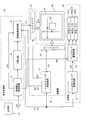
- FIG. 1 is a block diagram illustrating a configuration of a field sequential type liquid crystal display device according to a first embodiment of the present invention.
- FIG. It is a figure which shows the relationship between the vertical blanking period with which transparent area information was added, and the video display area in 1 frame period of 1st Embodiment.
- a 1st embodiment it is a figure which compares the case where transparent area information is expressed with the specific gradation value of each color component, and the case where it adds to a vertical blanking period.
- the field sequential type liquid crystal display device it is a diagram showing gradation values of each color component that can be used for video display by adding transparent area information during the vertical blanking period.
- FIG. 16 is a diagram illustrating an example in which one frame period is divided into five subframe periods in the modified examples of the first to fifth embodiments. It is a figure which shows handling a specific gradation value as a transparent gradation in the conventional liquid crystal display device of a field sequential system.
- FIG. 1 is a block diagram showing a configuration of a field sequential type liquid crystal display device according to a first embodiment of the present invention.
- the liquid crystal display device according to this embodiment is a display device that performs color display by a field sequential method in which one frame period is time-divided into three subframe periods.
- the liquid crystal display device includes a signal source 10, a signal processing unit 20, a driving unit 30, a liquid crystal panel 40, and a light source unit 50.
- the signal processing unit 20 includes a transparent gradation control circuit 21, a separation circuit 23, and a frequency conversion circuit 24.
- the drive unit 30 includes an LCD timing control circuit 31, a source driver 32, and a gate driver 33.
- the light source unit 50 includes an LED timing control circuit 51, a backlight driving circuit 52, and red, green, and blue LEDs (Light Emitting Diodes) 53r, 53g, and 53b that emit red, green, and blue light, respectively. Yes. When these LEDs 53r, 53g, and 53b are not distinguished, they may be referred to as “LEDs 53”.
- one frame period is 1/60 seconds, and subframe periods for displaying red, green, and blue images are each 1/180 seconds.
- the color depth of the red component (R component), green component (G component), and blue component (B component) included in the video signal DAT input from the signal source 10 to the signal processing unit 20 is 10 bits.
- the liquid crystal display device can express each color of red, green, and blue with 1024 gradations, approximately 1.70 billion colors (more precisely, 1024 ⁇ 1024 ⁇ 1024 colors) are displayed on the liquid crystal panel 40. can do.
- the color depth of each color component is not limited to 10 bits, and may be, for example, 8 bits, 12 bits, or 14 bits.
- the R component, G component, and B component may be collectively referred to as “each color component”.
- the signal source 10 transmits a video signal DAT representing a video displayed on the display unit 41 of the liquid crystal panel 40 and a control signal TS such as a vertical synchronization signal and a horizontal synchronization signal to the signal processing unit 20 every frame period.
- a control signal TS such as a vertical synchronization signal and a horizontal synchronization signal
- transparent area information Ita indicating whether or not to perform transparent display is added to each pixel forming unit 42 during the vertical blanking period of the video signal DAT.
- the transparent gradation control circuit 21 Upon receiving the video signal DAT from the signal source 10, the transparent gradation control circuit 21 reads the transparent area information Ita added to the video signal DAT and supplies it to the frequency conversion circuit 24.
- the transparent area information Ita is the same information as the LCD information Icd indicating whether or not the pixel forming portion 42 is transparent in each embodiment described later.
- the video signal DAT is input to the separation circuit 23.
- the separation circuit 23 separates the R component, the G component, and the B component from the video signal DAT, time-divides each color component, and sequentially outputs them to the frequency conversion circuit 24.
- the frequency conversion circuit 24 converts the frequency of each color component of the given video signal DAT from 1/60 seconds to 1/180 seconds. Further, the frequency conversion circuit 24 outputs the control signal TS and the transparent area information Ita included in the video signal DAT to the LCD timing control circuit 31.
- the LCD timing control circuit 31 is a control signal such as a source start pulse, a clock signal, and a latch strobe signal necessary for driving the source driver 32 based on the control signal TS and the transparent area information Ita given from the frequency conversion circuit 24.
- An SCT is generated and output to the source driver 32, and a control signal GCT such as a gate start pulse and a clock signal necessary for driving the gate driver 33 is generated and output to the gate driver 33.
- the LCD timing control circuit 31 uses the control signals SCT and GCT for driving the source driver 32 and the gate driver 33 as frequencies in order to synchronize the operation of the frequency conversion circuit 24 with the operations of the source driver 32 and the gate driver 33.
- the conversion circuit 24 is also provided. Based on the control signals SCT and GCT given from the LCD timing control circuit 31, the frequency conversion circuit 24 converts each color component of the video signal DAT given from the separation circuit 23 and the transparent area given from the transparent gradation control circuit 21. Information Ita is given to the source driver 32.
- a plurality of source lines SL, a plurality of gate lines GL, and a plurality of pixel formations corresponding to the intersections of the source lines SL and the gate lines GL are formed.
- a portion 42 is formed.
- a panel capable of high-speed response is used for the liquid crystal panel 40 so that an image of each color component can be displayed every 1/180 second.
- the display unit 41 only one pixel formation unit 42 connected to the source line SL and the gate line GL is shown for convenience.
- the source driver 32 drives signals for each color component from the R component, G component, and B component included in the video signal DAT supplied from the frequency conversion circuit 24. Voltages are generated in order, the drive signal voltages are time-divisionally applied to the source line SL in order, and the pixel forming unit 42 to be transparently displayed based on the transparent area information Ita has a transparent level corresponding to the transparent gradation. The application of the regulated voltage Vt is repeated every subframe period.
- the gate driver 33 Based on the control signal GCT supplied from the LCD timing control circuit 31, the gate driver 33 sequentially applies to the plurality of gate lines GL every subframe period to activate the gate lines GL one by one. Is repeated every subframe period.
- the frequency conversion circuit 24 controls the control signal TS and the transparent area information in order to control the turning on and off of the LED 53 that functions as a backlight in accordance with the timing at which the driving signal voltage of each color component is applied to the pixel forming unit 42. Ita is also given to the LED timing control circuit 51.
- the LED timing control circuit 51 generates a backlight control signal BCT for controlling lighting and extinguishing of the LED 53 based on the control signal TS and the transparent area information Ita, and provides the backlight driving circuit 52 with the backlight control signal BCT.
- a red LED (Light Emitting Diode) 53r, a green LED 53g, and a blue LED 53b that irradiate the liquid crystal panel 40 with red, green, and blue light, respectively, are disposed on the back side of the liquid crystal panel 40.
- the backlight control signal BCT provided from the LED timing control circuit 51 includes lighting times, extinguishing times, driving current values, and the like of the LEDs 53r, 53g, and 53b of the respective colors. At this time, if the drive current passed through the LED 53 arranged at the position corresponding to the pixel forming portion 42 is increased, the luminance of the LED increases, and the pixel forming portion 42 at the position corresponding to the LED is transparently displayed.
- the backlight drive circuit 52 turns on and off the LED 53 with a predetermined luminance based on the backlight control signal BCT provided from the LED timing control circuit 51, and also forms a pixel display section 42 to be transparently displayed.
- a large drive current is passed through the LED 53 at a position corresponding to.
- the drive current for the LED 53 is supplied from a power supply circuit (not shown).
- the driving signal voltage and the transparent gradation voltage Vt are applied to the source line SL, the scanning signal is applied to the gate line GL, and light of each color is irradiated from the LED 53 to the liquid crystal panel 40 in order.
- the driving signal voltage is applied to each pixel forming unit 42 of the display unit 41, and the video represented by the video signal DAT is displayed on the display unit 41.
- the pixel forming unit 42 to which the transparent gradation voltage Vt generated based on the transparent area information Ita is applied becomes transparent, and the background can be seen through the pixel forming unit 42.
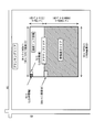
- FIG. 2 is a diagram illustrating a relationship between the vertical blanking period to which the transparent area information is added and the video display area in one frame period of the present embodiment.
- the horizontal synchronizing signal HS shown in FIG. 2 defines one horizontal scanning period
- the vertical synchronizing signal VS defines one vertical scanning period.
- an active area and a blanking area surrounding it are set.
- the blanking area includes a vertical blanking area and a horizontal blanking area.
- the upper and lower areas of the video display area are vertical blanking areas
- the left and right areas are horizontal blanking areas.
- the vertical synchronization signal VS and the horizontal synchronization signal HS are described as signal waveforms in the case of positive logic, but these signals may be signal waveforms in the case of negative logic.
- the active area includes a video display area composed of 1920 pixels in the horizontal direction and 1080 pixels in the vertical direction, and a back porch period in the vertical blanking period to which transparent area information is added (hereinafter, unless otherwise specified in the description of this embodiment).
- This area includes “vertical blanking period”.
- Each pixel forming unit 42 is composed of red, green, and blue sub-pixels (not shown). If the color depth of each color component in each sub-pixel is 10 bits, the number of bits A1 included in one horizontal scanning period of the video display area can be obtained by the following equation (1).
- A1 1920 ⁇ 3 ⁇ 10 (1)
- the transparent area information is 1-bit information indicating whether or not each pixel is transparent.
- the pixel forming unit 42 is not transparent when the transparent area information is “0”, and is transparent when the transparent area information is “1”. Therefore, the number of bits A2 of the transparent area information necessary to indicate whether or not all the pixels in the video display area are transparent is obtained by the following equation (2).
- A2 1920 ⁇ 1080 ⁇ 1 (2)
- the vertical data corresponding to 36 lines from the first data enable (Data Enable) in the vertical blanking period is used.
- a blanking period is required. Since this transparent area information is given as a part of the active area in the vertical blanking period, the active area included in the video signal DAT transmitted from the signal source 10 is (1080 + 36) lines.
- the vertical blanking period to which the transparent area information is added is adjacent to the video display area. Note that the vertical blanking period is set to include at least 36 lines or more so that the transparent area information of all the pixel forming portions 42 can be added.
- the transparent area information added in the vertical blanking period is adjacent to the video display area, but for example, information on the transparent area after 5 clocks from the falling edge of the vertical synchronization signal VS. Therefore, the transparent area information added during the vertical blanking period may not be adjacent to the video display area.
- the transparent area information is added to the back porch period of the vertical blanking period, but may be added to the front porch period of the vertical blanking period. In this case, the transparent area information added to the front porch period is not information in the current frame period but information in the next frame period.
- FIG. 3 is a diagram comparing the case where the transparent area information is represented by a specific gradation value of each color component and the case where it is added to the vertical blanking period.
- a video is displayed in an area of 1920 ⁇ 1080 pixels, which is a video display area, with an R component, a G component, and a B component having a color depth of 10 bits.
- the case of the present embodiment will be described as compared to the conventional case.
- each color component in the transparent display area, the 1023 gradation value of each color component is assigned to the transparent gradation. For this reason, when displaying an image in the image display area, each color component can be expressed only by 1023 gradations of 0 to 1022 gradation values, and pixel values (1023, 1023, 1023) are assigned to transparent gradations. The color represented by the pixel value cannot be displayed.
- each color component can be expressed by 1024 gradations of 0 to 1023 gradation values, and even when a transparent display area is provided, an image can be displayed in a full range of colors.
- FIG. 4 is a diagram showing gradation values of each color component that can be used when displaying an image by adding transparent area information during a vertical blanking period in a field sequential type liquid crystal display device.
- each color has 1024 gradations from 0 gradation value to 1023 gradation value. It is possible to display.
- pixel values (1023, 1023, 1023) are different from the case shown in FIG. 14 by adding transparent area information during the vertical blanking period. Need not be assigned to the transparent gradation, and the color represented by the pixel value can also be used when displaying an image. As a result, the liquid crystal display device can display images in all colors even when performing transparent display.
- the liquid crystal display device in the field sequential type liquid crystal display device, by adding transparent area information during the vertical blanking period, a part of the color depth of each of the R component, G component, and B component is assigned to the transparent gradation. There is no need. Accordingly, the liquid crystal display device can display an image using all colors even when performing transparent display.
- FIG. 5 is a block diagram showing a configuration of a liquid crystal display device according to the second embodiment of the present invention. Since the liquid crystal display device according to the present embodiment is composed of the same circuit as the circuit constituting the liquid crystal display device shown in FIG. 1, the same reference numerals as those of the liquid crystal display device are given to the respective circuits of the liquid crystal display device. It is attached. However, in these liquid crystal display devices, since the connection destination of the transparent gradation control circuit 21 is partially different, this point will be described.
- the transparent gradation control circuit 21 is only connected to the separation circuit 23 and the frequency conversion circuit 24. In addition, it is also connected to the backlight drive circuit 52. This is due to the following reason.
- the transparent area information is represented by 1-bit information indicating whether or not each pixel is transparent.
- the transparent area information is only information indicating whether or not each pixel forming unit 42 is transparent (hereinafter referred to as “LCD information Icd” in the present embodiment).
- the transparent gradation control circuit 21 is also connected to the backlight drive circuit 52 in order to give the LED information Ied included in the transparent area information added in the vertical blanking period to the backlight drive circuit 52.
- the LCD information Icd may be referred to as “transparent display information”, and the LED information Ied may be referred to as “transparency information”.
- the liquid crystal display device is a see-through type display device in which the background of the liquid crystal panel 40 can be seen through
- the number of LEDs 53 arranged on the back side of the liquid crystal panel 40 is made smaller than usual.
- the transparency of the pixel forming unit 42 is set by adjusting the luminance of the LED 53, so that the pixel forming unit 42 has a one-to-one correspondence with the pixel forming unit 42 in order to set the transparency. It is preferable to arrange the LED 53 in the above. However, if the number of LEDs 53 is increased, light from the background is less likely to be transmitted through the liquid crystal panel 40 during transparent display, so that the background is less visible through the liquid crystal panel 40. Therefore, it is preferable to increase the number of LEDs 53 within a range where the background of the liquid crystal panel 40 is sufficiently visible.
- the transparent area information used in the present embodiment represents the transparent state of one pixel with 2-bit information. Of these bits, 1 bit is LCD information Icd indicating whether or not the pixel forming portion 42 is transparent. Similarly to the case of the first embodiment, “0” is set when the pixel forming portion 42 is not transparent. ", And" 1 "if it is transparent.
- the other 1 bit is LED information Ied indicating the transparency of the pixel forming unit 42 when the pixel forming unit 42 is transparent.
- the transparency of the pixel forming portion 42 is determined by the luminance of the LED 53 of each color. If the luminance of the LED 53 is increased, the transparency of the pixel forming portion 42 is increased, and if the luminance of the LED 53 is decreased, the transparency of the pixel forming portion 42 is decreased. Therefore, by setting the LED information Ied indicating the luminance of the LED 53 to “0” or “1”, it is possible to set the pixel forming portion 42 to be transparently displayed to one of two levels of transparency. Specifically, the drive current of the LED 53 is increased or decreased by controlling the backlight drive circuit 52.
- the liquid crystal display device can set the transparency of the pixel forming unit 42 that should perform transparent display, based on the LED information Ied included in the transparent area information.
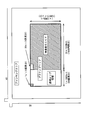
- FIG. 6 is a diagram illustrating the relationship between the vertical blanking period to which the transparent area information is added and the video display area in one frame period of the present embodiment.
- the active area includes a video display area composed of 1920 pixels in the horizontal direction and 1080 pixels in the vertical direction, and a back porch period (hereinafter referred to as the present embodiment) of the vertical blanking period to which transparent area information is added.
- the present embodiment a back porch period
- Each pixel forming unit 42 includes three sub-pixels (not shown) of red, green, and blue. If the color depth of each color component in each sub-pixel is 10 bits, the number of bits B1 included in one horizontal scanning period of the video display area can be obtained by the following equation (4).
- B1 1920 ⁇ 3 ⁇ 10 (4)
- the transparent area information added during the vertical blanking period is different from the number of bits in the video display area, and is 1-bit LCD information Icd indicating whether or not each pixel forming unit 42 is transparent, and see-through.
- the information is made up of a total of 2 bits of 1-bit LED information Ied representing the transparency of the pixel forming section 42 set as described above, and these are given continuously. Therefore, the total number of bits B2 of the transparent area information in one frame period is obtained by the following equation (5).
- B2 1920 ⁇ 1080 ⁇ 2 (5)
- the LED information is described as 1-bit information, but may be multi-bit information.
- the transparency of the pixel forming portion to be transparently displayed can be set to more stages instead of being set to one of the two stages.
- the transparent area information is described as being added to the back porch period of the vertical blanking period, but can be added to the front porch period.
- the transparent area information added to the front porch period is not information in the current frame period but information in the next frame period.
- the liquid crystal display device in the field sequential type liquid crystal display device, by adding the transparent area information during the vertical blanking period, the R component, the G component, and the B component. It is not necessary to assign a part of each color depth to the transparent area information. Accordingly, the liquid crystal display device can display an image using all colors even when performing transparent display.
- the liquid crystal display device can set the transparency of the pixel forming portion 42 to be transparently displayed by adjusting the luminance of the LED 53 based on the LED information Ied.
- the liquid crystal display device according to the third embodiment of the present invention adds 1-bit transparent area information to the horizontal blanking period.
- the configuration of the liquid crystal display device according to the present embodiment is the same as the configuration of the liquid crystal display device shown in FIG. 1, the block diagram and description of the liquid crystal display device according to the present embodiment are omitted.
- FIG. 7 is a diagram illustrating the relationship between the horizontal blanking period to which the transparent area information is added and the video display area in one frame period of the present embodiment.
- the active area is composed of a video display area composed of 1920 pixels in the horizontal direction and 1080 pixels in the vertical direction, and the horizontal blanking period to which the transparent area information is added is the active area. Is not included.
- Each pixel forming unit 42 includes three sub pixel forming units (not shown) of red, green, and blue. If the color depth of these sub-pixels is 10 bits, the number of bits of one pixel forming unit 42 is (3 ⁇ 10) bits.
- the transparent area information is only the LCD information Icd indicating whether or not each pixel forming unit 42 is transparent, one pixel forming unit 42 has one bit. Therefore, the number of pixels Lh of the transparent area information corresponding to 1920 pixels included in one horizontal scanning period (one line) of the video display area is obtained by the following equation (7).
- the transparent area information for 64 pixels may be added for one line in the horizontal blanking period. Therefore, in the present embodiment, transparent area information is added to 64 pixels from the falling edge of the vertical synchronization signal VS for each line in the horizontal blanking period.
- the transparent area information for 64 pixels is added for each line from the first data enable in the horizontal blanking period. Is repeated for 1080 lines. Since this transparent area information is added in the horizontal blanking period separately from the active area, the video signal DAT corresponding to 1920 pixels of the active area for each line from the signal source 10 and 64 pixels separately from the active area. Transparent area information is transmitted. For this reason, as shown in FIG. 7, the horizontal blanking period to which the transparent area information is added is not adjacent to the video display area. In this case, the horizontal blanking period is set to include at least 64 pixels per line so that the transparent area information of all the pixel forming portions 42 can be added.
- the transparent area information is described as being added to the back porch period of the horizontal blanking period. However, it may be added to the front porch period. In this case, the transparent area information added to the front porch period is not information in the current frame period, but information in the next frame period.
- the liquid crystal display device by adding transparent area information in the horizontal blanking period, similarly to the case of adding transparent area information in the vertical blanking period, the R component, G A part of the color depths of the component and the B component may not be used as the transparent gradation. Accordingly, the liquid crystal display device can display an image using all colors even when performing transparent display.
- FIG. 8 is a diagram showing another relationship between the video display area and the horizontal blanking period in which transparent area information is added in one frame period.
- 64 pixels from the time when the vertical synchronization signal VS falls are used as the transparent area information.
- the horizontal blanking period with the transparent area information added is set at a position away from the video display area. Therefore, as shown in FIG. 8, by increasing the data enable transmitted from the signal source 10, an active area including a video display area and a horizontal blanking period to which transparent area information is added is formed.
- This active area includes 1984 pixels in total, including 1920 pixels of the video display area and 64 pixels from the rise time of the data enable, and further includes 1080 such lines. Yes. Therefore, unlike the case shown in FIG. 7, the video display area and the transparent area information added in the horizontal blanking period are adjacent to each other. Since the effect in this case is the same as the effect of the liquid crystal display device shown in FIG.
- the transparent area information is 1-bit information. However, as long as it is within the range of the number of bits that can be added during the horizontal blanking period, information of 2 bits or more may be added as the transparent area information, as in the second embodiment.
- the transparent area information is represented by 2 bits as in the liquid crystal display device according to the second embodiment. However, unlike the case of the first embodiment, 1 bit of 2-bit transparent area information is added to the vertical blanking period, and the other 1 bit is added to the horizontal blanking period.
- the configuration of the liquid crystal display device according to the present embodiment is the same as the configuration of the liquid crystal display device shown in FIG.
- the transparent area information transmitted from the signal source 10 includes 2-bit information.
- the 1-bit information of the transparent area information is LCD information Icd that is “0” when each pixel forming unit 42 is not transparent and “1” when each pixel forming unit 42 is transparent. This information is information given to the source driver 32 via the frequency conversion circuit 24.
- the other 1-bit information is LED information Ied indicating the transparency of the pixel forming unit 42 to be transparently displayed. Specifically, when the LED information Ied is “0”, the drive current value of each LED 53 is decreased to lower the luminance of the LED 53, and the transparency of the pixel forming portion 42 is set to be lower.
- the LED information Ied is “1”
- the drive current value of each LED 53 is increased to increase the luminance of the LED 53, and the transparency of the pixel forming portion 42 is set to be high.
- the LED information Ied can set the transparency of the pixel forming portion 42 to be transparently displayed by controlling the luminance of the LED 53.
- FIG. 9 is a diagram showing the relationship between the vertical and horizontal blanking periods to which the transparent area information is added and the video display area in one frame period of the present embodiment.
- each color depth of the R component, the G component, and the B component is 10 bits, and the LCD information and the LED information are each 1 bit, the LED information is added to the vertical blanking period.
- the information for LCD is added to the horizontal blanking period and transmitted.
- the number of pixels in the video display area is 1920 ⁇ 1080 pixels.
- 64 pixels are required for each horizontal period as determined in the third embodiment. Therefore, the horizontal width of the active area is 1984 pixels when combined with the 1920 pixels of the video display area.
- the number of lines Lv3 required when adding the LED information to the vertical blanking period is obtained by the following formula (10).
- the number of lines in the vertical direction of the active area is (35 + 1080) lines.
- LED information for 35 lines is transmitted from the first data enable in the vertical blanking period.
- the LCD information for 64 pixels (one line) is transmitted from the first data enable in the horizontal blanking period.
- a video signal DAT for 1920 pixels (one line) is transmitted.
- the transmission of the LCD information and the video signal DAT for one line is completed, the transmission of the LCD information and the video signal DAT for the next one line is performed. In this way, the LCD information and the video signal DAT are transmitted for one line, for a total of 1080 lines. In this way, the video signal and the transparent area information included in the active area are transmitted.
- each color of the R component, the G component, and the B component is obtained by adding LCD information during the horizontal blanking period. It becomes unnecessary to use a part of the depth as a transparent gradation. Accordingly, the liquid crystal display device can display an image using all colors even when performing transparent display. Further, by adding the LED information during the vertical blanking period, the liquid crystal display device can set the transparency by adjusting the luminance of the LEDs 53 of each color included in the backlight unit based on the information.
- the transparency information is not set to one of the two levels, as in the case of the second embodiment. It can also be set in stages.
- the LED information is added to the vertical blanking period and the LCD information is added to the horizontal blanking period.
- the LED information may be added to the horizontal blanking period, and the LCD information may be added to the vertical blanking period. In this case, the same effect as described above can be obtained.
- the liquid crystal display device according to the fifth embodiment of the present invention does not add transparent area information to the vertical or horizontal blanking period, It is added to the signal DAT. That is, a new number of bits is added in addition to the number of bits representing the color depth of the R component, G component, and B component included in the video signal DAT, and the added number of bits is assigned to the transparent area information.
- the configuration of the liquid crystal display device according to the present embodiment is the same as the configuration of the liquid crystal display device shown in FIG.
- each color component of the video signal DAT is assigned to the color depth of each color component as a 10-bit signal, and each color component is further expanded by adding 2 bits. 2 bits are assigned to the transparent area information. For this reason, each color component of the video signal is apparently 12 bits.
- FIG. 10 is a diagram showing how to use the number of bits representing the color depth of the R component, the G component, and the B component included in the video signal DAT. More specifically, FIG. 10A is a diagram showing the number of bits of the R component, G component, and B component, and FIG. 10B is the number of bits representing the color depths of the R component, G component, and B component. It is a figure which shows the bit number allocated to transparent area information. As shown in FIG. 10, the number of bits of the R component, G component, and B component are all expanded to 12 bits. However, among them, 10 bits are assigned to each color component for the color depth of the video, and the remaining 2 bits are assigned to the transparent area information.
- the transparent gradation control circuit 21 of the liquid crystal display device If the 2-bit transparent area information added to the video signal DAT is read by the transparent gradation control circuit 21 of the liquid crystal display device, 1-bit information of the 2-bit information included in the transparent area information is used as LCD information. The signal is supplied to the frequency conversion circuit 24, and the other 1 bit is supplied to the backlight drive circuit 52 as LED information. Since the subsequent operation of the liquid crystal display device is the same as that described in the fourth embodiment, the description thereof is omitted.
- the color depth of each color component can be represented by 10 bits.
- the pixel values (1023, 1023, 1023) can be assigned to the transparent gradation, and the color represented by the pixel value can also be used when displaying an image.
- the liquid crystal display device can display images using all colors even when performing transparent display.
- 2 bits are added to 10 bits representing each color component of the video signal in order to add the LCD information and the LED information included in the transparent area information.
- only LCD information may be added to one of the two added bits, and LED information may be added to the horizontal blanking period or vertical blanking period, or only LED information is added.
- the information for LCD may be added to the horizontal blanking period or the vertical blanking period in addition to one of the two bits.
- a bit added to 10 bits representing each color component of the video signal may be referred to as an “additional transparent area”.
- the liquid crystal display device is not a field sequential type liquid crystal display device described in each of the first to fifth embodiments but a color filter type liquid crystal display device, and is not a see-through type. / A display device that displays only a color image every 60 seconds.
- FIG. 11 is a block diagram showing a configuration of the liquid crystal display device according to the present embodiment.
- the configuration of the liquid crystal display device is substantially the same as the configuration of the liquid crystal display device shown in FIG.
- hidden area information is added to the vertical blanking period instead of the transparent area information.
- the fill information Inp included in the hidden area information is “0”
- an image is displayed on the pixel formation unit 47 of the display unit 46 of the liquid crystal panel 45.
- the fill information Inp is “1”
- the pixel formation is performed.
- the portion 47 is filled so that no video is displayed. Therefore, in the liquid crystal display device, a hidden area control circuit 22 is provided instead of the transparent gradation control circuit 21.
- the hidden area control circuit 22 reads the paint information Inp added during the vertical blanking period and supplies it to the source driver 32, the LCD timing control circuit 31, and the LED timing control circuit 51.
- the source driver 32 drives signals for each color component from the R component, G component, and B component included in the video signal DAT supplied from the frequency conversion circuit 24. Voltages are generated in order, and the driving signal voltages are time-divisionally applied to the source line SL in order. Further, applying the fill gradation voltage Vn corresponding to the fill gradation to the pixel forming portion 47 to be filled based on the fill information Inp is repeated every subframe period.
- the separation circuit 23 and the frequency conversion circuit 24 may not be included or may be included. However, when the separation circuit 23 and the frequency conversion circuit 24 are included as shown in FIG. 11, it is necessary to stop their operations. Therefore, in FIG. 11, the separation circuit 23 and the frequency conversion circuit 24 are surrounded by a dotted line to indicate that the operation is stopped.
- the liquid crystal panel 40 included in the liquid crystal display device shown in FIG. 1 is replaced with a liquid crystal panel 45 on which a color filter is formed. Even when the information added in the vertical blanking period is hidden area information, the apparatus can display an image by the color filter method or can fill the hidden pixel forming unit 42 so that the image cannot be displayed.
- the liquid crystal display device usable in this embodiment can be manufactured by simply replacing the field sequential type liquid crystal panel 40 with the color filter type liquid crystal panel 45. it can. Thereby, the manufacturing cost of the liquid crystal display device which can be used in this embodiment can be suppressed at low cost.
- FIG. 12 is a diagram showing the relationship between the video display area and the vertical blanking period to which the hidden area information is added in one frame period of the present embodiment.
- This embodiment corresponds to the case where hidden area information is added to the vertical blanking period instead of transparent area information in the case of the first embodiment. Therefore, as shown in FIG. 12, as the number of lines necessary for adding 1-bit hidden area information corresponding to each of 1920 ⁇ 1080 pixels in the video display area during the vertical blanking period of the video display area, 36 lines are required as determined in the first embodiment. Therefore, the (36 + 1080) lines obtained by combining 1080 lines in the video display area and 36 lines to which hidden area information is added are active areas transmitted from the signal source 10.
- the hidden area information may be added to the horizontal blanking period instead of being added to the vertical blanking period.
- the hidden area information may be represented by a plurality of bits, and a part of the hidden area information may be used as character information for displaying a character or the like on a filled pixel, for example.
- the LCD information and the character information included in the hidden area information may be added together in either the vertical blanking period or the horizontal blanking period, or for example, the LCD information may be added to the vertical blanking period and the horizontal blanking period.
- the blanking period may be given to one of the blanking periods, and the character information may be added to the other blanking period.
- the hidden area information is added to the vertical blanking period, so that it is not necessary to assign a part of each color depth of the R component, the G component, and the B component to the hidden area information.
- the liquid crystal display device can express the video in all colors even when providing a hidden area where the video is not displayed.
- the display unit 46 of the liquid crystal panel 45 can be provided with a pixel forming unit 47 filled with a predetermined color, or black characters can be displayed on the pixel forming unit 42 painted with white or the like, for example.
- the transparent area information and the hidden area information may be collectively referred to as “display area information”, and the state when the pixel forming unit 42 is in the transparent state and the filled state are collectively referred to as the “display state”. There is a case.
- the liquid crystal display device divides one frame period into three subframe periods by time division by a field sequential method, and red, green, and blue images are time-divided in each subframe period. Then, color images were displayed by displaying them sequentially.
- FIG. 13 is a diagram illustrating an example when one frame period is divided into five subframe periods.
- a white subframe (W subframe) period for displaying a white image is added before and after a subframe period for displaying red, green, and blue images, and one frame period is divided into five frames. You may comprise by a sub-frame period.
- Such driving can also be realized in the liquid crystal display device shown in FIG.
- the separation circuit 23 separates the R component, the G component, and the B component included in the video signal for each frame period, and before and after reading them by the frequency conversion circuit 24, the W subframe period is set. In the W subframe period, each color component is read out simultaneously. In this case, since 5 subframe periods are provided in 1/60 second which is one frame period, the frequency conversion circuit 24 needs to convert each subframe period to 1/300 seconds.
- the present invention is applicable to a display device such as a liquid crystal display device that performs color display by a field sequential method or a color filter method.
Landscapes
- Engineering & Computer Science (AREA)
- Physics & Mathematics (AREA)
- Computer Hardware Design (AREA)
- General Physics & Mathematics (AREA)
- Theoretical Computer Science (AREA)
- Multimedia (AREA)
- Signal Processing (AREA)
- Chemical & Material Sciences (AREA)
- Crystallography & Structural Chemistry (AREA)
- Computer Graphics (AREA)
- Control Of Indicators Other Than Cathode Ray Tubes (AREA)
Abstract
従来、透明表示エリアでは、各色成分の1023階調値を透明階調に割り当てていた。このため、映像表示エリアに映像を表示する際に、各色成分を0~1022階調値の1023階調でしか表すことができず、画素値(1023、1023、1023)を透明階調に割り当てる必要がなくなり、当該画素値で表される色を表示することができなかった。そこで、透明エリア情報を映像信号の垂直ブランキング期間に付加するようにすれば、画素値(1023、1023、1023)も映像を表示するために使用可能になる。これにより、各色成分を0~1023階調値の1024階調で表すことが可能になり、透明表示エリアを設けた場合にも映像をフルレンジの色で表示することが可能になる。
Description
本発明は、液晶表示装置に関し、特に、フィールドシーケンシャル方式やカラーフィルタ方式でカラー表示を行う液晶表示装置に関する。
カラー表示を行う液晶表示装置の多くは、1つの画素を3分割したサブ画素に対応してそれぞれ、赤色(R)、緑色(G)、および青色(B)の光を透過させるカラーフィルタを備えている。しかし、液晶表示パネルに照射されるバックライト光の約2/3がカラーフィルタに吸収されるために、カラーフィルタ方式の液晶表示装置は光利用効率が低いという問題を有する。そこで、カラーフィルタを用いずにカラー表示を行うフィールドシーケンシャル方式の液晶表示装置が注目されている。
フィールドシーケンシャル方式では、1画面の表示期間である1フレーム期間は3つのサブフレーム期間に分割される。第1のサブフレーム期間には、映像信号の赤色成分を入力しつつ赤色の光源を発光させることによって、赤色の画面が表示される。第2のサブフレーム期間には、映像信号の緑色成分を入力しつつ緑色の光源を発光させることによって、緑色の画面が表示される。第3のサブフレーム期間には、映像信号の青色成分を入力しつつ青色の光源を発光させることによって、青色の画面が表示される。このようにして、フィールドシーケンシャル方式の液晶表示装置は赤色、緑色、青色の各画面を順に表示するので、視聴者は残像効果によりカラー映像を視認することができる。このように、フィールドシーケンシャル方式の液晶表示装置では、カラーフィルタが不要になるので、カラーフィルタ方式の液晶表示装置に比べて光の利用効率が約3倍に向上する。
特許文献1には、ブランキング期間にコンテンツ識別情報が付加された映像信号を受信すれば、当該コンテンツ識別情報に基づいてコンテンツの種類に応じた最適な処理を映像信号に対して行うことが記載されている。また、特許文献2には、OSD(On Screen Display)用の映像を表示する第1映像信号と、OSD用の映像とは別の映像を表示する第2映像信号の2系統の映像信号を扱うシステムにおいて、OSD用の情報を第2映像信号のブランキング期間に付加して送信することが記載されている。
図14は、従来のフィールドシーケンシャル方式の液晶表示装置において、特定の階調値を透明階調として扱うことを示す図である。図14に示すように、例えば赤色、緑色、青色の各色成分が10ビットである場合、通常の画像だけを表示するのであれば、各色成分についてそれぞれ0階調値から1023階調値までの1024階調で表示することが可能である。しかし、シースルー(透明)表示を行う場合には、各色成分の特定の階調値(例えば1023階調値)を透明階調に割り当てる。このように、当該液晶表示装置において、特定の階調値を透明階調に割り当てれば、当該特定の階調値は映像を表示するために使用できない。このため、表示可能なすべての色を使用して映像を表示することができないという問題がある。
また、特許文献1に記載の発明によれば、映像信号のブランキング期間に挿入されているのはコンテンツの種類を識別するための情報だけであるため、表示パネルに透明エリアを設定する場合には、映像信号の特定の階調値を透明階調に割り当てなければならない。同様に、特許文献2に記載の発明においても、OSD用の情報を第2映像信号のブランキング期間に送信することは記載されているが、透明エリア情報もブランキング期間に送信することは記載されていない。そこで、透明エリア情報を追加しようとすれば第2映像信号の特定の階調値を透明階調に割り当てなければならない。このように、いずれの場合も表示部に透明エリアを設定するために、映像信号の特定の階調値を透明階調に割り当てなければならない。この場合、透明階調に割り当てた特定の階調値は映像信号として使用できないので、表示可能なすべての色で映像を表現することはできない。
そこで、本発明は、表示可能なすべての色を使用して映像を表示することが可能な液晶表示装置を提供することを目的とする。
本発明の第1の局面は、信号源から入力された映像信号によって表される映像を表示する液晶表示装置であって、
複数の画素形成部を含む表示部と、
前記映像信号に基づき前記表示部に前記映像を表示する駆動部と、
前記映像信号に付加して入力された表示エリア情報に基づき前記画素形成部の表示状態を制御する信号処理部とを備え、
前記表示エリア情報は、前記映像信号に付加して与えられ、
前記駆動部は、前記表示エリア情報によって特定された前記画素形成部の表示状態を制御すると共に、前記表示エリア情報によって特定されていない前記画素形成部に前記映像を表示することを特徴とする。
複数の画素形成部を含む表示部と、
前記映像信号に基づき前記表示部に前記映像を表示する駆動部と、
前記映像信号に付加して入力された表示エリア情報に基づき前記画素形成部の表示状態を制御する信号処理部とを備え、
前記表示エリア情報は、前記映像信号に付加して与えられ、
前記駆動部は、前記表示エリア情報によって特定された前記画素形成部の表示状態を制御すると共に、前記表示エリア情報によって特定されていない前記画素形成部に前記映像を表示することを特徴とする。
本発明の第2の局面は、本発明の第1の局面において、
前記液晶表示装置は、前記表示部に光を照射するために、1フレーム期間を複数のサブフレーム期間に分割し、前記サブフレーム期間毎に指定された色の光を発する複数色の光源と前記光源を駆動するバックライト駆動回路とを含む光源部をさらに備えることによって、前記サブフレーム期間毎に異なる色の画面を表示し、
前記表示エリア情報は、前記画素形成部毎に透明表示すべきか否かを示す透明表示情報を含む透明エリア情報であり、
前記信号処理部は、前記映像信号に付加された前記表示エリア情報から前記透明表示情報を読み出す透明階調制御回路と、前記透明階調制御回路に接続され、前記1フレーム期間の前記映像信号を色毎に分離する分離回路と、前記サブフレーム期間毎に分離された1または2以上の色の画面を表示する前記映像信号を分離回路から読み出して周波数を変換し、前記透明階調制御回路によって読み出された前記透明表示情報と共に、前記駆動部に与える周波数変換回路とを含み、
前記駆動部は、前記透明表示情報によって特定された前記画素形成部を透明表示すると共に、前記透明表示情報によって特定されていない前記画素形成部に前記映像を表示することを特徴とする。
本発明の第3の局面は、本発明の第2の局面において、
前記透明エリア情報は、前記映像信号の垂直ブランキング期間、水平ブランキング期間、および前記映像信号の追加透明エリアのうちの少なくともいずれかに付加されていることを特徴とする。
前記透明エリア情報は、前記映像信号の垂直ブランキング期間、水平ブランキング期間、および前記映像信号の追加透明エリアのうちの少なくともいずれかに付加されていることを特徴とする。
本発明の第4の局面は、本発明の第2の局面において、
前記透明エリア情報は、前記映像信号の垂直ブランキング期間または水平ブランキング期間の少なくともいずれかと、前記映像信号の追加透明エリアとにそれぞれ付加されていることを特徴とする。
前記透明エリア情報は、前記映像信号の垂直ブランキング期間または水平ブランキング期間の少なくともいずれかと、前記映像信号の追加透明エリアとにそれぞれ付加されていることを特徴とする。
本発明の第5の局面は、本発明の第3または第4の局面において、
前記透明エリア情報は、前記光源の輝度を制御することによって、透明表示する前記画素形成部の透明度を設定する透明度情報をさらに含み、
前記光源は1または2以上の前記画素形成部毎に配置された発光ダイオードからなり、前記バックライト駆動回路は、前記透明度情報に基づいて前記発光ダイオードの駆動電流値を調整して輝度を制御することを特徴とする。
前記透明エリア情報は、前記光源の輝度を制御することによって、透明表示する前記画素形成部の透明度を設定する透明度情報をさらに含み、
前記光源は1または2以上の前記画素形成部毎に配置された発光ダイオードからなり、前記バックライト駆動回路は、前記透明度情報に基づいて前記発光ダイオードの駆動電流値を調整して輝度を制御することを特徴とする。
本発明の第6の局面は、本発明の第5の局面において、
前記透明エリア情報は、前記垂直ブランキング期間または前記水平ブランキング期間のバックポーチ期間またはフロントポーチ期間に付加されることを特徴とする。
前記透明エリア情報は、前記垂直ブランキング期間または前記水平ブランキング期間のバックポーチ期間またはフロントポーチ期間に付加されることを特徴とする。
本発明の第7の局面は、本発明の第5の局面において、
前記透明表示情報と前記透明度情報は、前記垂直ブランキング期間、前記水平ブランキング期間、および前記映像信号の追加透明エリアのうちのいずれかに連続して付加されることを特徴とする。
前記透明表示情報と前記透明度情報は、前記垂直ブランキング期間、前記水平ブランキング期間、および前記映像信号の追加透明エリアのうちのいずれかに連続して付加されることを特徴とする。
本発明の第8の局面は、本発明の第5の局面において、
前記透明表示情報は、前記垂直ブランキング期間、前記水平ブランキング期間、および前記映像信号の追加透明エリアのうちのいずれかに付加され、前記透明度情報は残りのいずれかに付加されることを特徴とする。
前記透明表示情報は、前記垂直ブランキング期間、前記水平ブランキング期間、および前記映像信号の追加透明エリアのうちのいずれかに付加され、前記透明度情報は残りのいずれかに付加されることを特徴とする。
本発明の第9の局面は、本発明の第5の局面において、
前記透明表示情報および前記透明度情報のうち少なくともいずれかは、1水平走査期間毎に垂直同期信号の立ち下がり時または立ち上がり時から前記水平ブランキング期間に付加されることを特徴とする。
前記透明表示情報および前記透明度情報のうち少なくともいずれかは、1水平走査期間毎に垂直同期信号の立ち下がり時または立ち上がり時から前記水平ブランキング期間に付加されることを特徴とする。
本発明の第10の局面は、本発明の第5の局面において、
前記透明表示情報および前記透明度情報のうち少なくともいずれかは、前記映像信号が表示されるエリアと隣接する前記水平ブランキング期間に付加されることを特徴とする。
前記透明表示情報および前記透明度情報のうち少なくともいずれかは、前記映像信号が表示されるエリアと隣接する前記水平ブランキング期間に付加されることを特徴とする。
本発明の第11の局面は、本発明の第1の局面において、
前記表示エリア情報は、前記画素形成部を所定の色で塗りつぶすか否かを示す塗りつぶし情報を含む隠しエリア情報であり、
前記信号処理部は、前記映像信号の垂直ブランキング期間および水平ブランキング期間のいずれかに付加された前記塗りつぶし情報を読み出す隠しエリア制御回路を含み、
前記駆動部は、前記塗りつぶし情報によって特定された前記画素形成部を所定の色で塗りつぶすと共に、前記塗りつぶし情報によって特定されていない前記画素形成部に前記映像を表示することを特徴とする。
前記表示エリア情報は、前記画素形成部を所定の色で塗りつぶすか否かを示す塗りつぶし情報を含む隠しエリア情報であり、
前記信号処理部は、前記映像信号の垂直ブランキング期間および水平ブランキング期間のいずれかに付加された前記塗りつぶし情報を読み出す隠しエリア制御回路を含み、
前記駆動部は、前記塗りつぶし情報によって特定された前記画素形成部を所定の色で塗りつぶすと共に、前記塗りつぶし情報によって特定されていない前記画素形成部に前記映像を表示することを特徴とする。
本発明の第12の局面は、本発明の第11の局面において、
前記隠しエリア情報は、文字を表示するための文字情報をさらに含み、
前記塗りつぶし情報および前記文字情報は、前記垂直ブランキング期間および前記水平ブランキング期間のいずれか一方にまとめて付加され、または前記垂直ブランキング期間および前記水平ブランキング期間にそれぞれ分けて付加され、
前記駆動部は、前記塗りつぶし情報に基づいて塗りつぶされた前記画素形成部に前記文字情報に基づき文字を表示することを特徴とする。
前記隠しエリア情報は、文字を表示するための文字情報をさらに含み、
前記塗りつぶし情報および前記文字情報は、前記垂直ブランキング期間および前記水平ブランキング期間のいずれか一方にまとめて付加され、または前記垂直ブランキング期間および前記水平ブランキング期間にそれぞれ分けて付加され、
前記駆動部は、前記塗りつぶし情報に基づいて塗りつぶされた前記画素形成部に前記文字情報に基づき文字を表示することを特徴とする。
上記第1の局面によれば、画素形成部の表示状態を表す表示エリア情報を、映像信号に付加して与えることにより、表示エリア情報によって特定された画素形成部は所定の表示状態になる。これにより、映像信号に含まれる各色成分の色深度の一部を表示エリア情報に割り当てる必要がなくなるので、画素形成部を表示エリア情報によって決まる表示状態にする際に、画素形成部に表示される映像をすべての色を使用して表示することができる。
上記第2の局面によれば、フィールドシーケンシャル方式の液晶表示装置において、画素形成部毎に透明表示すべきか否かを示す透明表示情報を、映像信号に付加して与える。これにより、透明表示エリア情報によって特定された画素形成部は透明表示される。このため、映像信号に含まれる各色成分の色深度の一部を透明表示情報に割り当てる必要がなくなるので、画素形成部を透明表示する際に、透明表示しない画素形成部に表示される映像をすべての色を使用して表示することができる。
上記第3の局面によれば、透明表示情報は、映像信号の垂直ブランキング期間、水平ブランキング期間、および画像信号の追加透明エリアの少なくもいずれかに付加されるので、映像信号に含まれる各色成分の色深度の一部を透明表示情報に割り当てる必要がなくなる。これにより、画素形成部を透明表示する際に、透明表示しない画素形成部に表示される映像をすべての色を使用して表示することができる。
上記第4の局面によれば、透明表示情報は、映像信号の垂直ブランキング期間および水平ブランキング期間のいずれかと、画像信号の追加透明エリアとにそれぞれ付加されるので、映像信号に含まれる各色成分の色深度の一部を透明表示情報に割り当てる必要がなくなる。これにより、画素形成部を透明表示する際に、透明表示しない画素形成部に表示される映像をすべての色を使用して表示することができる。
上記第5の局面によれば、透明エリア情報には、光源の輝度を制御することによって画素形成部の透明度を設定する透明度情報も含まれている。画素形成部に対応して配置された発光ダイオードの駆動電流値を透明度情報に基づいて調整することにより、発光ダイオードの輝度を制御し、透明表示される画素形成部の透明度を設定することができる。
上記第6の局面によれば、透明エリア情報は、垂直ブランキング期間または水平ブランキング期間のバックポーチ期間またはフロントポーチ期間に付加される。
上記第7の局面によれば、透明表示情報と透明度情報は、垂直ブランキング期間、水平ブランキング期間、および映像信号の追加透明エリアのいずれかに連続して付加される。
上記第8の局面によれば、透明表示情報は、垂直ブランキング期間、水平ブランキング期間、および映像信号の追加透明エリアのいずれかに付加され、透明度情報は残りのいずれかに付加される。例えば、透明表示情報が垂直ブランキング期間に付加されれば、透明度情報は、水平ブランキング期間および映像信号の追加透明エリアのいずれかに付加される。
上記第9の局面によれば、透明エリア情報に含まれる透明表示情報および透明度情報のうち少なくともいずれかは、水平ブランキング期間に付与される際に、1水平走査期間毎に垂直同期信号の立ち下がり時または立ち上がり時から付加される。
上記第10の局面によれば、透明エリア情報に含まれる透明表示情報および透明度情報のうち少なくともいずれかは、映像信号が表示されるエリアと隣接する水平ブランキング期間に付与される。
上記第11の局面によれば、画素形成部毎に塗りつぶすべきか否かを示す塗りつぶし情報を、映像信号の垂直ブランキング期間および水平ブランキング期間の少なくもいずれか一方に付加して与える。これにより、塗りつぶし情報によって特定された画素形成部は所定の色で塗りつぶした状態で表示される。このため、映像信号に含まれる各色成分の色深度の一部を塗りつぶし情報に割り当てる必要がなくなるので、画素形成部を塗りつぶす際に、塗りつぶさない画素形成部に表示される映像をすべての色を使用して表示することができる。
上記第12の局面によれば、隠しエリア情報には、塗りつぶした画素形成部に文字を表示するための文字情報がさらに含まれている。この文字情報は塗りつぶし情報と共に、垂直ブランキング期間および前記水平ブランキング期間のいずれか一方にまとめて付加され、またはそれぞれを分けて付加される。この文字情報は塗りつぶした画素形成部に与えられるので、塗りつぶした画素形成部に文字が表示される。
<1.第1の実施形態>
<1.1 液晶表示装置の構成>
図1は、本発明の第1の実施形態に係るフィールドシーケンシャル方式の液晶表示装置の構成を示すブロック図である。本実施形態に係る液晶表示装置は、1フレーム期間を3つのサブフレーム期間に時分割するフィールドシーケンシャル方式によってカラー表示を行う表示装置である。図1に示すように、この液晶表示装置は、信号源10、信号処理部20、駆動部30、液晶パネル40、および光源部50を備えている。
<1.1 液晶表示装置の構成>
図1は、本発明の第1の実施形態に係るフィールドシーケンシャル方式の液晶表示装置の構成を示すブロック図である。本実施形態に係る液晶表示装置は、1フレーム期間を3つのサブフレーム期間に時分割するフィールドシーケンシャル方式によってカラー表示を行う表示装置である。図1に示すように、この液晶表示装置は、信号源10、信号処理部20、駆動部30、液晶パネル40、および光源部50を備えている。
信号処理部20は、透明階調制御回路21、分離回路23、および周波数変換回路24を備えている。駆動部30は、LCDタイミング制御回路31、ソースドライバ32、及およびゲートドライバ33を備えている。光源部50は、LEDタイミング制御回路51、バックライト駆動回路52、および、赤色、緑色、青色の光をそれぞれ発する赤色、緑色、青色の各LED(Light Emitting Diode)53r、53g、53bを備えている。これらのLED53r、53g、53bを区別しない場合には「LED53」という場合がある。
以下の説明では、例えば1フレーム期間を1/60秒とし、赤色、緑色、青色の映像を表示するサブフレーム期間をそれぞれ1/180秒とする。また、信号源10から信号処理部20に入力される映像信号DATに含まれる赤色成分(R成分)、緑色成分(G成分)、および青色成分(B成分)の色深度はそれぞれ10ビットであるとする。この場合、液晶表示装置は、赤色、緑色、青色の各色をそれぞれ1024階調で表現できるので、約10.7億色(正確には1024×1024×1024色)の色を液晶パネル40に表示することができる。なお、各色成分の色深度は10ビットに限定されず、例えば8ビット、12ビット、14ビットなどであってもよい。なお、R成分、G成分、B成分をまとめて「各色成分」という場合がある。
信号源10は、液晶パネル40の表示部41に表示される映像を表す映像信号DAT、および垂直同期信号や水平同期信号などの制御信号TSを1フレーム期間毎に信号処理部20に送信する。また、詳しくは後述するが、映像信号DATの垂直ブランキング期間には、画素形成部42毎に透明表示すべきか否かを示す透明エリア情報Itaが付加されている。信号源10から映像信号DATを受信した透明階調制御回路21は、映像信号DATに付加されている透明エリア情報Itaを読み出し、周波数変換回路24に与える。なお、透明エリア情報Itaは、後述する各実施形態において画素形成部42が透明であるか否かを表すLCD用情報Icdと同じ情報である。
次に、映像信号DATは分離回路23に入力される。分離回路23は、映像信号DATからR成分、G成分、B成分を分離し、各色成分を時分割して順に周波数変換回路24に出力する。周波数変換回路24は、与えられた映像信号DATの各色成分の周波数を1/60秒から1/180秒に変換する。また、周波数変換回路24は、映像信号DATに含まれる制御信号TSおよび透明エリア情報ItaをLCDタイミング制御回路31に出力する。
LCDタイミング制御回路31は、周波数変換回路24から与えられた制御信号TSおよび透明エリア情報Itaに基づき、ソースドライバ32を駆動するために必要なソーススタートパルス、クロック信号、ラッチストローブ信号などの制御信号SCTを生成してソースドライバ32に出力し、ゲートドライバ33を駆動するために必要なゲートスタートパルスおよびクロック信号などの制御信号GCTを生成してゲートドライバ33に出力する。
また、LCDタイミング制御回路31は、周波数変換回路24の動作をソースドライバ32およびゲートドライバ33の動作と同期させるために、ソースドライバ32およびゲートドライバ33を駆動するための制御信号SCT、GCTを周波数変換回路24にも与える。周波数変換回路24は、LCDタイミング制御回路31から与えられた制御信号SCT、GCTに基づき、分離回路23から与えられた映像信号DATの各色成分と、透明階調制御回路21から与えられた透明エリア情報Itaをソースドライバ32に与える。
液晶パネル40の表示部41には、複数本のソースラインSLと、複数本のゲートラインGLと、これらのソースラインSLとゲートラインGLとの交差点に対応して設けられた複数個の画素形成部42が形成されている。液晶パネル40には、1/180秒毎に各色成分の映像を表示できるように、高速応答が可能なパネルが使用される。なお、表示部41には、便宜上ソースラインSLおよびゲートラインGLに接続された1つの画素形成部42だけが示されている。
ソースドライバ32は、LCDタイミング制御回路31から与えられた制御信号SCTに基づいて、周波数変換回路24から与えられた映像信号DATに含まれるR成分、G成分、B成分から各色成分の駆動用信号電圧を順に生成し、それらの駆動用信号電圧を時分割してソースラインSLに順に印加し、また透明エリア情報Itaに基づき透明表示すべき画素形成部42には透明階調に応じた透明階調電圧Vtを印加することを1サブフレーム期間毎に繰り返す。
ゲートドライバ33は、LCDタイミング制御回路31から与えられた制御信号GCTに基づいて、1サブフレーム期間毎に複数本のゲートラインGLに順に印加して、ゲートラインGLを1本ずつアクティブにすることを1サブフレーム期間毎に繰り返す。
周波数変換回路24は、各色成分の駆動用信号電圧が画素形成部42に印加されるタイミングに合わせて、バックライトとして機能するLED53の点灯および消灯を制御するために、制御信号TSおよび透明エリア情報ItaをLEDタイミング制御回路51にも与える。LEDタイミング制御回路51は、当該制御信号TSおよび透明エリア情報Itaに基づいてLED53の点灯および消灯を制御するためのバックライト制御信号BCTを生成し、バックライト駆動回路52に与える。
液晶パネル40の背面側には、赤色、緑色、青色の光を液晶パネル40にそれぞれ照射する赤色LED(Light Emitting Diode)53r、緑色LED53g、青色LED53bが配置されている。LEDタイミング制御回路51から与えられるバックライト制御信号BCTには、各色のLED53r、53g、53bの点灯時刻、消灯時刻、および駆動電流値などが含まれている。このとき、画素形成部42に対応する位置に配置されたLED53に流す駆動電流を大きくすれば、当該LEDの輝度が大きくなり、当該LEDに対応する位置の画素形成部42は透明表示される。そこで、バックライト駆動回路52は、LEDタイミング制御回路51から与えられたバックライト制御信号BCTに基づいて、LED53を所定の輝度で点灯させたり消灯させたりすると共に、透明表示すべき画素形成部42に対応する位置のLED53に大きな駆動電流を流す。なお、LED53の駆動電流は、図示しない電源回路から供給される。
以上のようにして、ソースラインSLに駆動用信号電圧および透明階調電圧Vtが印加され、ゲートラインGLに走査信号が印加され、LED53から液晶パネル40に各色の光が順に照射される。これにより、表示部41の各画素形成部42に駆動用信号電圧が印加され、映像信号DATによって表される映像が表示部41に表示される。また透明エリア情報Itaに基づいて生成された透明階調電圧Vtが印加された画素形成部42は透明になり、当該画素形成部42を通して背景が透けて見えるようになる。
<1.2 液晶表示装置の動作>
図2は、本実施形態の1フレーム期間において、透明エリア情報が付加された垂直ブランキング期間と映像表示エリアとの関係を示す図である。図2に示す水平同期信号HSは1水平走査期間を規定し、垂直同期信号VSは1垂直走査期間を規定する。水平同期信号HSと垂直同期信号VSによって規定される1フレーム期間には、アクティブエリアとそれを取り囲むブランキングエリアが設定されている。ブランキングエリアには、垂直ブランキングエリアと水平ブランキングエリアが含まれている。図2に示すブランキングエリアのうち、映像表示エリアの上下のエリアが垂直ブランキングエリアであり、左右のエリアが水平ブランキングエリアである。なお、図2では、垂直同期信号VSおよび水平同期信号HSは、正論理の場合の信号波形として記載されているが、これらの信号は負論理の場合の信号波形であってもよい。
図2は、本実施形態の1フレーム期間において、透明エリア情報が付加された垂直ブランキング期間と映像表示エリアとの関係を示す図である。図2に示す水平同期信号HSは1水平走査期間を規定し、垂直同期信号VSは1垂直走査期間を規定する。水平同期信号HSと垂直同期信号VSによって規定される1フレーム期間には、アクティブエリアとそれを取り囲むブランキングエリアが設定されている。ブランキングエリアには、垂直ブランキングエリアと水平ブランキングエリアが含まれている。図2に示すブランキングエリアのうち、映像表示エリアの上下のエリアが垂直ブランキングエリアであり、左右のエリアが水平ブランキングエリアである。なお、図2では、垂直同期信号VSおよび水平同期信号HSは、正論理の場合の信号波形として記載されているが、これらの信号は負論理の場合の信号波形であってもよい。
アクティブエリアは、水平方向に1920画素、垂直方向に1080画素からなる映像表示エリアと、透明エリア情報が付加された垂直ブランキング期間のバックポーチ期間(以下、本実施形態の説明では特に断らない限り「垂直ブランキング期間」という)を含むエリアである。各画素形成部42は、赤色、緑色、青色の各サブ画素(図示しない)からなる。各サブ画素における各色成分の色深度をそれぞれ10ビットとすれば、映像表示エリアの1水平走査期間に含まれるビット数A1は次式(1)によって求められる。
A1=1920×3×10 … (1)
A1=1920×3×10 … (1)
透明エリア情報は、映像表示エリアの色深度と異なり、画素毎に透明であるか否かを表す1ビットの情報である。例えば、画素形成部42は、透明エリア情報が“0”の場合には透明ではないとし、“1”の場合には透明であるとする。そこで、映像表示エリアの全画素について透明であるか否かを表すために必要な透明エリア情報のビット数A2は次式(2)によって求められる。
A2=1920×1080×1 … (2)
A2=1920×1080×1 … (2)
上式(1)および上式(2)から、すべての画素について透明であるか否かを表す透明エリア情報を付加するために必要な垂直ブランキング期間のライン数Lv1は次式(3)によって求められる。
Lv1=A2/A1=36 … (3)
Lv1=A2/A1=36 … (3)
上式(3)より、すべての画素について透明であるか否かを示す透明エリア情報を付加するためには、垂直ブランキング期間の1つ目のデータイネーブル(Data Enable)から36ライン分の垂直ブランキング期間が必要になる。この透明エリア情報はアクティブエリアの一部として垂直ブランキング期間に付与されるので、信号源10から送信される映像信号DATに含まれるアクティブエリアは(1080+36)ラインになる。このように、透明エリア情報が付加された垂直ブランキング期間は映像表示エリアに隣接している。なお、垂直ブランキング期間は、すべての画素形成部42の透明エリア情報を付加できるように、少なくとも36ライン以上のラインを含むように設定されている。
なお、上記説明では、垂直ブランキング期間に付加された透明エリア情報が映像表示エリアに隣接している場合について説明したが、例えば垂直同期信号VSの立ち下がり時から5クロック後から透明エリアの情報があると決めることも可能であるため、垂直ブランキング期間に付加された透明エリア情報は映像表示エリアに隣接していなくてもよい。また、 上記説明では、透明エリア情報は垂直ブランキング期間のバックポーチ期間に付加される場合について説明したが、垂直ブランキング期間のフロントポーチ期間に付加されてもよい。この場合、フロントポーチ期間に付加した透明エリア情報は、現在のフレーム期間における情報ではなく、次のフレーム期間における情報になる。
図3は、透明エリア情報を各色成分の特定の階調値によって表した場合と、垂直ブランキング期間に付加した場合とを比較した図である。図3に示すように、映像表示エリアである1920×1080画素のエリアに色深度が10ビットのR成分、G成分、B成分によって映像を表示する。このような映像表示エリアに透明にしたい画素形成部42からなる透明表示エリアを設ける場合について、従来の場合と比較して、本実施形態の場合を説明する。
従来、透明表示エリアでは、各色成分の1023階調値を透明階調に割り当てていた。このため、映像表示エリアに映像を表示する際に、各色成分を0~1022階調値の1023階調でしか表すことができず、画素値(1023、1023、1023)を透明階調に割り当てる必要があり、当該画素値で表される色を表示することができなかった。
そこで、透明エリア情報を映像信号DATの垂直ブランキング期間に付加するようにすれば、画素値(1023、1023、1023)を透明階調に割り当てる必要がなくなり、当該画素値も映像を表示するために使用可能になる。これにより、各色成分を0~1023階調値の1024階調で表すことが可能になり、透明表示エリアを設けた場合にも映像をフルレンジの色で表示することが可能になる。
また、図4は、フィールドシーケンシャル方式の液晶表示装置において、垂直ブランキング期間に透明エリア情報を付加することによって映像を表示する際に使用可能な各色成分の階調値を示す図である。図4に示すように、例えば映像信号DATに含まれる赤色、緑色、青色の各色成分の色深度が10ビットである場合、各色はそれぞれ0階調値から1023階調値までの1024階調で表示することが可能である。このように、液晶表示装置の表示部41に透明表示を行う際に、垂直ブランキング期間に透明エリア情報を付加することにより、図14に示す場合と異なり、画素値(1023、1023、1023)を透明階調に割り当てる必要がなくなり、当該画素値で表される色も映像を表示する際に使用することができる。その結果、液晶表示装置は透明表示を行う際にも、映像をすべての色で表示することが可能になる。
<1.3 効果>
本実施形態によれば、フィールドシーケンシャル方式の液晶表示装置において、垂直ブランキング期間に透明エリア情報を付加することにより、R成分、G成分、B成分の各色深度の一部を透明階調に割り当てる必要がなくなる。これにより、液晶表示装置は透明表示を行う際にも、すべての色を使用して映像を表示することが可能になる。
本実施形態によれば、フィールドシーケンシャル方式の液晶表示装置において、垂直ブランキング期間に透明エリア情報を付加することにより、R成分、G成分、B成分の各色深度の一部を透明階調に割り当てる必要がなくなる。これにより、液晶表示装置は透明表示を行う際にも、すべての色を使用して映像を表示することが可能になる。
<2.第2の実施形態>
<2.1 液晶表示装置の構成>
図5は、本発明の第2の実施形態に係る液晶表示装置の構成を示すブロック図である。本実施形態に係る液晶表示装置は、図1に示す液晶表示装置を構成する回路と同じ回路から構成されているので、液晶表示装置の各回路には、液晶表示装置の回路と同じ参照符号を付している。ただし、これらの液晶表示装置では透明階調制御回路21の接続先が一部異なっているので、その点について説明する。
<2.1 液晶表示装置の構成>
図5は、本発明の第2の実施形態に係る液晶表示装置の構成を示すブロック図である。本実施形態に係る液晶表示装置は、図1に示す液晶表示装置を構成する回路と同じ回路から構成されているので、液晶表示装置の各回路には、液晶表示装置の回路と同じ参照符号を付している。ただし、これらの液晶表示装置では透明階調制御回路21の接続先が一部異なっているので、その点について説明する。
図5に示すように、本実施形態に係る液晶表示装置では、図1に示す液晶表示装置の場合と異なり、透明階調制御回路21は分離回路23および周波数変換回路24に接続されているだけでなく、さらにバックライト駆動回路52にも接続されている。これは以下の理由による。図1に示す液晶表示装置では、透明エリア情報は画素毎に透明であるか否かを表す1ビットの情報で表されていた。しかし、本実施形態では、詳しくは後述するが、透明エリア情報は、画素形成部42毎に透明であるか否かを表す情報(以下、本実施形態では「LCD用情報Icd」という)だけではなく、さらに透明である場合に画素形成部42の透明度を設定するための情報(以下、本実施形態では「LED用情報Ied」という)も含む。そこで、透明階調制御回路21は、垂直ブランキング期間に付加された透明エリア情報に含まれるLED用情報Iedをバックライト駆動回路52に与えるために、バックライト駆動回路52にも接続されている。なお、LCD用情報Icdを「透明表示情報」といい、LED用情報Iedを「透明度情報」という場合がある。
また、液晶表示装置は液晶パネル40の背景が透けて見えるシースルータイプの表示装置であるため、液晶パネル40の裏面側に配置するLED53の個数を通常の場合よりも少なくしている。特に本実施形態では、LED53の輝度を調整することによって画素形成部42の透明度を設定するので、画素形成部42毎に透明度を設定するために、画素形成部42と1対1で対応するようにLED53を配置することが好ましい。しかし、LED53の個数を増やせば、透明表示の際に背景からの光が液晶パネル40を透過しにくくなるので、液晶パネル40を通して背景が見えにくくなる。そこで、液晶パネル40の背景が十分見える範囲でLED53の個数を増やすことが好ましい。
次に、液晶表示装置に与えられるLED用情報Iedについて説明する。本実施形態において使用される透明エリア情報は、第1の実施形態において使用される透明エリア情報と異なり、1つの画素の透明状態を2ビットの情報で表す。このうち、1ビットは画素形成部42が透明であるか否かを表すLCD用情報Icdであり、第1の実施形態の場合と同様に、当該画素形成部42が透明ではない場合に“0”とし、透明である場合に“1”とする。
他の1ビットは、当該画素形成部42が透明である場合において、画素形成部42の透明度を表すLED用情報Iedである。画素形成部42の透明度は、各色のLED53の輝度によって決まり、LED53の輝度を大きくすれば画素形成部42の透明度も高くなり、LED53の輝度を小さくすれば画素形成部42の透明度も低くなる。そこで、LED53の輝度を表すLED用情報Iedを“0”または“1”に設定することにより、透明表示すべき画素形成部42を2段階の透明度のいずれかに設定することが可能になる。具体的には、バックライト駆動回路52を制御することによりLED53の駆動電流を増加または減少させる。駆動電流値を大きくすれば、LED53の輝度が大きくなるので、画素形成部42の透明度は高くなる。一方、駆動電流値を小さくすれば、LED53の輝度は小さくなるので、画素形成部42の透明度は低くなる。このようにして、液晶表示装置は、透明エリア情報に含まれるLED用情報Iedに基づき、透明表示を行うべき画素形成部42の透明度を設定することができる。
<2.2 液晶表示装置の動作>
図6は、本実施形態の1フレーム期間において、透明エリア情報が付加された垂直ブランキング期間と映像表示エリアとの関係を示す図である。図6に示すように、アクティブエリアは、水平方向に1920画素、垂直方向に1080画素からなる映像表示エリアと、透明エリア情報が付加された垂直ブランキング期間のバックポーチ期間(以下、本実施形態の説明では特に断らない限り「垂直ブランキング期間」という)を含むエリアである。各画素形成部42は、赤色、緑色、青色の3つのサブ画素(図示しない)からなる。各サブ画素における各色成分の色深度をそれぞれ10ビットとすれば、映像表示エリアの1水平走査期間に含まれるビット数B1は次式(4)によって求められる。
B1=1920×3×10 … (4)
また、垂直ブランキング期間に付加された透明エリア情報は、映像表示エリアのビット数と異なり、画素形成部42毎に透明であるか否かを表す1ビットのLCD用情報Icdと、シースルーになるように設定された画素形成部42の透明度を表す1ビットのLED用情報Iedの合計2ビットの情報からなり、しかもそれらは連続して与えられている。したがって、1フレーム期間における透明エリア情報の全ビット数B2は次式(5)によって求められる。
B2=1920×1080×2 … (5)
B2=1920×1080×2 … (5)
上式(4)および上式(5)からすべての画素形成部42の透明エリア情報を表示するために必要な垂直ブランキング期間のライン数Lv2は次式(6)によって求められる。
Lv2=B2/B1=72 … (6)
Lv2=B2/B1=72 … (6)
上式(6)より、映像表示エリアの各画素形成部42に透明エリア情報を与えるためには、垂直ブランキング期間の1つ目のデータイネーブルから72ライン分の垂直ブランキング期間が必要であることがわかる。この透明エリア情報はアクティブエリアの一部として垂直ブランキング期間に付与されるので、信号源10から送信される映像信号DATに含まれるアクティブエリアは(1080+72)ラインになる。このように、透明エリア情報が付加された垂直ブランキング期間は映像表示エリアに隣接している。
なお、上記説明では、LED用情報は1ビットの情報であるとして説明したが、複数ビットの情報であってもよい。この場合、透明表示される画素形成部の透明度を2段階のいずれかに設定するのではなく、より多くの段階に設定することができる。
また上記説明では、透明エリア情報は垂直ブランキング期間のバックポーチ期間に付加されるとして説明したが、フロントポーチ期間に付加することもできる。この場合、フロントポーチ期間に付加した透明エリア情報は、現在のフレーム期間における情報ではなく、次のフレーム期間における情報になる。
<2.3 効果>
本実施形態によれば、第1の実施形態の場合と同様に、フィールドシーケンシャル方式の液晶表示装置において、垂直ブランキング期間に透明エリア情報を付加することにより、R成分、G成分、B成分の各色深度の一部を透明エリア情報に割り当てる必要がなくなる。これにより、液晶表示装置は透明表示を行う際にも、すべての色を使用して映像を表示することが可能になる。
本実施形態によれば、第1の実施形態の場合と同様に、フィールドシーケンシャル方式の液晶表示装置において、垂直ブランキング期間に透明エリア情報を付加することにより、R成分、G成分、B成分の各色深度の一部を透明エリア情報に割り当てる必要がなくなる。これにより、液晶表示装置は透明表示を行う際にも、すべての色を使用して映像を表示することが可能になる。
さらに、本実施形態の透明エリア情報には、画素形成部42が透明であるか否かを表すLCD用情報Icdだけではなく、当該画素形成部42が透明である場合にその透明度を設定するLED用情報Iedも含んでいる。このため、液晶表示装置は、LED用情報Iedに基づいてLED53の輝度を調整することにより、透明表示すべき画素形成部42の透明度を設定することが可能になる。
<3.第3の実施形態>
本発明の第3の実施形態に係る液晶表示装置は、第1の実施形態に係る液晶表示装置と異なり、1ビットの透明エリア情報を水平ブランキング期間に付加している。しかし、本実施形態に係る液晶表示装置の構成は、図1に示す液晶表示装置の構成と同じであるため、本実施形態に係る液晶表示装置のブロック図および説明を省略する。
本発明の第3の実施形態に係る液晶表示装置は、第1の実施形態に係る液晶表示装置と異なり、1ビットの透明エリア情報を水平ブランキング期間に付加している。しかし、本実施形態に係る液晶表示装置の構成は、図1に示す液晶表示装置の構成と同じであるため、本実施形態に係る液晶表示装置のブロック図および説明を省略する。
<3.1 液晶表示装置の動作>
本実施形態では、透明エリア情報を、水平ブランキング期間のバックポーチ期間(以下、本実施形態の説明では特に断らない限り「水平ブランキング期間」という)に付加する。図7は、本実施形態の1フレーム期間において、透明エリア情報が付加された水平ブランキング期間と映像表示エリアとの関係を示す図である。
本実施形態では、透明エリア情報を、水平ブランキング期間のバックポーチ期間(以下、本実施形態の説明では特に断らない限り「水平ブランキング期間」という)に付加する。図7は、本実施形態の1フレーム期間において、透明エリア情報が付加された水平ブランキング期間と映像表示エリアとの関係を示す図である。
図7に示すように、本実施形態では、アクティブエリアは、水平方向に1920画素、垂直方向に1080画素からなる映像表示エリアからなり、透明エリア情報が付加された水平ブランキング期間はアクティブエリアには含まれていない。各画素形成部42は、赤色、緑色、青色の3つのサブ画素形成部(図示しない)からなる。これらのサブ画素の色深度をそれぞれ10ビットとすれば、1つの画素形成部42のビット数は(3×10)ビットになる。一方、透明エリア情報は画素形成部42毎に透明であるか否かを表すLCD用情報Icdだけであるため、1つの画素形成部42あたり1ビットである。そこで、映像表示エリアの1水平走査期間(1ライン)に含まれる1920画素分に相当する透明エリア情報の画素数Lhは、次式(7)により求められる。
Lh=1920/(3×10)=64 … (7)
Lh=1920/(3×10)=64 … (7)
つまり、1ラインに含まれる画素数分の透明エリア情報を送信するためには、水平ブランキング期間の1ラインについて64画素分の透明エリア情報を付加すればよい。そこで、本実施形態では、水平ブランキング期間のうち1ライン毎に垂直同期信号VSの立ち下がり時から64画素分に透明エリア情報を付加する。
このように、映像表示エリアの各画素形成部42について透明エリア情報を与えるためには、水平ブランキング期間の1つ目のデータイネーブルから1ライン毎に64画素分の透明エリア情報を付加することを1080ラインについて繰り返し行う。この透明エリア情報はアクティブエリアとは別に、水平ブランキング期間に付加されるので、信号源10からは1ライン毎にアクティブエリアの1920画素分の映像信号DATと、アクティブエリアとは別に64画素分の透明エリア情報が送信される。このため、図7に示すように、透明エリア情報が付加された水平ブランキング期間と映像表示エリアとは隣接していない。この場合、水平ブランキング期間は、すべての画素形成部42の透明エリア情報を付加できるように、1ラインあたり少なくとも64画素分の画素数を含むように設定されている。
なお、上記説明では、透明エリア情報は水平ブランキング期間のバックポーチ期間に付加されるとして説明したが、フロントポーチ期間に付加することもできる。この場合、フロントポーチ期間に付加した透明エリア情報は、現在のフレーム期間における情報ではなく、次にフレーム期間における情報になる。
<3.2 効果>
本実施形態によれば、フィールドシーケンシャル方式の液晶表示装置において、水平ブランキング期間に透明エリア情報を付加することにより、垂直ブランキング期間に透明エリア情報を付加した場合と同様に、R成分、G成分、B成分の各色深度の一部を透明階調として使用しなくてもよい。これにより、液晶表示装置は透明表示を行う際にも、すべての色を使用して映像を表示することが可能になる。
本実施形態によれば、フィールドシーケンシャル方式の液晶表示装置において、水平ブランキング期間に透明エリア情報を付加することにより、垂直ブランキング期間に透明エリア情報を付加した場合と同様に、R成分、G成分、B成分の各色深度の一部を透明階調として使用しなくてもよい。これにより、液晶表示装置は透明表示を行う際にも、すべての色を使用して映像を表示することが可能になる。
<3.3 変形例>
図8は、映像表示エリアと、1フレーム期間に透明エリア情報が付加された水平ブランキング期間との他の関係を示す図である。本実施形態では、垂直同期信号VSの立ち下がり時から64画素分を透明エリア情報とした。この場合、透明エリア情報を付加した水平ブランキング期間は、映像表示エリアから離れた位置に設定された。そこで、図8に示すように、信号源10から送信されるデータイネーブルを増やすことによって、映像表示エリアと透明エリア情報が付加された水平ブランキング期間とからなるアクティブエリアを形成する。このアクティブエリアには、1ラインあたり、映像表示エリアの1920画素分と、データイネーブルの立ち上がり時から64画素分とを合わせて1984画素分が含まれ、さらにそのようなラインが1080ライン含まれている。このため、図7に示す場合と異なり、映像表示エリアと水平ブランキング期間に付加された透明エリア情報とは隣接している。この場合の効果は、図7に示す液晶表示装置による効果と同じであるので、その説明を省略する。
図8は、映像表示エリアと、1フレーム期間に透明エリア情報が付加された水平ブランキング期間との他の関係を示す図である。本実施形態では、垂直同期信号VSの立ち下がり時から64画素分を透明エリア情報とした。この場合、透明エリア情報を付加した水平ブランキング期間は、映像表示エリアから離れた位置に設定された。そこで、図8に示すように、信号源10から送信されるデータイネーブルを増やすことによって、映像表示エリアと透明エリア情報が付加された水平ブランキング期間とからなるアクティブエリアを形成する。このアクティブエリアには、1ラインあたり、映像表示エリアの1920画素分と、データイネーブルの立ち上がり時から64画素分とを合わせて1984画素分が含まれ、さらにそのようなラインが1080ライン含まれている。このため、図7に示す場合と異なり、映像表示エリアと水平ブランキング期間に付加された透明エリア情報とは隣接している。この場合の効果は、図7に示す液晶表示装置による効果と同じであるので、その説明を省略する。
また、本実施形態では、透明エリア情報は1ビットの情報であるとした。しかし、水平ブランキング期間に付加できるビット数の範囲であれば、第2の実施形態の場合と同じように、透明エリア情報として2ビットまたはそれ以上のビット数の情報を付加してもよい。
<4.第4の実施形態>
本発明の第4の実施形態に係る液晶表示装置は、第2の実施形態に係る液晶表示装置と同様に透明エリア情報は2ビットで表される。しかし、第1の実施形態の場合と異なり、2ビットの透明エリア情報のうち1ビットを垂直ブランキング期間に付加し、他の1ビットを水平ブランキング期間に付加している。なお、本実施形態に係る液晶表示装置の構成は、図2に示す液晶表示装置の構成と同じであるため、そのブロック図および説明を省略する。
本発明の第4の実施形態に係る液晶表示装置は、第2の実施形態に係る液晶表示装置と同様に透明エリア情報は2ビットで表される。しかし、第1の実施形態の場合と異なり、2ビットの透明エリア情報のうち1ビットを垂直ブランキング期間に付加し、他の1ビットを水平ブランキング期間に付加している。なお、本実施形態に係る液晶表示装置の構成は、図2に示す液晶表示装置の構成と同じであるため、そのブロック図および説明を省略する。
<4.1 液晶表示装置の動作>
本実施形態では、第2の実施形態の場合と同様に、信号源10から送信される透明エリア情報には2ビットの情報が含まれている。この透明エリア情報のうち1ビットの情報は、各画素形成部42が透明ではない場合には“0”とし、透明である場合には“1”とするLCD用情報Icdである。この情報は、周波数変換回路24を介してソースドライバ32に与えられる情報である。また、他の1ビットの情報は透明表示を行うべき画素形成部42の透明度を表すLED用情報Iedである。具体的には、LED用情報Iedが“0”の場合には各LED53の駆動電流値を小さくしてLED53の輝度を低くし、画素形成部42の透明度を低く設定する。LED用情報Iedが“1”の場合には各LED53の駆動電流値を大きくしてLED53の輝度を高くし、画素形成部42の透明度を高く設定する。このように、LED用情報IedはLED53の輝度を制御することにより、透明表示を行うべき画素形成部42の透明度を設定することができる。
本実施形態では、第2の実施形態の場合と同様に、信号源10から送信される透明エリア情報には2ビットの情報が含まれている。この透明エリア情報のうち1ビットの情報は、各画素形成部42が透明ではない場合には“0”とし、透明である場合には“1”とするLCD用情報Icdである。この情報は、周波数変換回路24を介してソースドライバ32に与えられる情報である。また、他の1ビットの情報は透明表示を行うべき画素形成部42の透明度を表すLED用情報Iedである。具体的には、LED用情報Iedが“0”の場合には各LED53の駆動電流値を小さくしてLED53の輝度を低くし、画素形成部42の透明度を低く設定する。LED用情報Iedが“1”の場合には各LED53の駆動電流値を大きくしてLED53の輝度を高くし、画素形成部42の透明度を高く設定する。このように、LED用情報IedはLED53の輝度を制御することにより、透明表示を行うべき画素形成部42の透明度を設定することができる。
図9は、本実施形態の1フレーム期間において、透明エリア情報が付加された垂直および水平ブランキング期間と映像表示エリアとの関係を示す図である。本実施形態では、R成分、G成分、B成分の各色深度が10ビットであり、LCD用情報およびLED用情報がそれぞれ1ビットである場合に、LED用情報を垂直ブランキング期間に付加して送信し、LCD用情報を水平ブランキング期間に付加して送信する。
映像表示エリアの画素数は1920×1080画素である。LCD用情報の1水平期間分を送信するためには、第3の実施形態で求めたように1水平期間毎に64画素分が必要になる。このため、アクティブエリアの水平方向の幅は映像表示エリアの1920画素分と合わせて1984画素分になる。
また、LED用情報を垂直ブランキング期間に付加するために必要な情報のビット数は次式(8)で表される。
C1=1920×1080×1 … (8)
C1=1920×1080×1 … (8)
各画素形成部42は、赤色、緑色、青色の3つのサブ画素からなり、各サブ画素の色深度を10ビットとすれば、LCD用情報が付加された水平ブランキング期間の画素数を含むアクティブエリアの水平方向の幅は上述のように1984画素であるので、そのビット数C2は次式(9)により求められる。
C2=1984×3×10 … (9)
C2=1984×3×10 … (9)
上式(8)と上式(9)から、LED用情報を垂直ブランキング期間に付加する際に必要なライン数Lv3は次式(10)により求められる。
Lv3=C1/C2=35 … (10)
その結果、アクティブエリアの垂直方向のライン数は(35+1080)ラインになる。
Lv3=C1/C2=35 … (10)
その結果、アクティブエリアの垂直方向のライン数は(35+1080)ラインになる。
そこで、信号源10から送信される映像信号DATには、まず垂直ブランキング期間の1つ目のデータイネーブルから35ライン分のLED用情報を送信する。LED用情報の送信が終了すると、水平ブランキング期間の1つ目のデータイネーブルから64画素分(1ライン分)のLCD用情報を送信する。次に、1920画素分(1ライン分)の映像信号DATを送信する。1ライン分のLCD用情報と映像信号DATの送信が終了すると、次の1ライン分のLCD用情報と映像信号DATの送信を行う。このようにして、LCD用情報と映像信号DATを1ライン分ずつ、全部で1080ライン分を送信する。このようにして、アクティブエリアに含まれる映像信号および透明エリア情報を送信する。
<4.2 効果>
本実施形態によれば、第2実施形態の場合と同様に、フィールドシーケンシャル方式の液晶表示装置において、水平ブランキング期間にLCD用情報を付加することにより、R成分、G成分、B成分の各色深度の一部を透明階調として使用しなくてもよくなる。これにより、液晶表示装置は透明表示を行う際にも、すべての色を使用して映像を表示することが可能になる。また、垂直ブランキング期間にLED用情報を付加することにより、液晶表示装置は、当該情報に基づいてバックライトユニットに含まれる各色のLED53の輝度を調整して、透明度を設定することができる。
本実施形態によれば、第2実施形態の場合と同様に、フィールドシーケンシャル方式の液晶表示装置において、水平ブランキング期間にLCD用情報を付加することにより、R成分、G成分、B成分の各色深度の一部を透明階調として使用しなくてもよくなる。これにより、液晶表示装置は透明表示を行う際にも、すべての色を使用して映像を表示することが可能になる。また、垂直ブランキング期間にLED用情報を付加することにより、液晶表示装置は、当該情報に基づいてバックライトユニットに含まれる各色のLED53の輝度を調整して、透明度を設定することができる。
なお、透明度情報を複数ビットの情報とすることにより、第2の実施形態の場合と同様に、透明表示される画素形成部の透明度を2段階のいずれかに設定するのではなく、より多くの段階に設定することもできる。
また、LED用情報を垂直ブランキング期間に付加し、LCD用情報を水平ブランキング期間に付加するとして説明した。しかし、LED用情報を水平ブランキング期間に付加し、LCD用情報を垂直ブランキング期間に付加してもよい。この場合も上記効果と同様の効果が得られる。
<5.第5の実施形態>
本発明の第5の実施形態に係る液晶表示装置は、上記第1~第4の実施形態に係る液晶表示装置と異なり、透明エリア情報を垂直または水平ブランキング期間に付加するのではなく、映像信号DATに付加する。すなわち、映像信号DATに含まれるR成分、G成分、B成分の色深度を表すビット数とは別に新たなビット数を追加し、追加したビット数を透明エリア情報に割り当てる。なお、本実施形態に係る液晶表示装置の構成は、図1に示す液晶表示装置の構成と同じであるため、そのブロック図および説明を省略する。
本発明の第5の実施形態に係る液晶表示装置は、上記第1~第4の実施形態に係る液晶表示装置と異なり、透明エリア情報を垂直または水平ブランキング期間に付加するのではなく、映像信号DATに付加する。すなわち、映像信号DATに含まれるR成分、G成分、B成分の色深度を表すビット数とは別に新たなビット数を追加し、追加したビット数を透明エリア情報に割り当てる。なお、本実施形態に係る液晶表示装置の構成は、図1に示す液晶表示装置の構成と同じであるため、そのブロック図および説明を省略する。
本実施形態では、上記各実施形態の場合と異なり、映像信号DATの各色成分を10ビットの信号として各色成分の色深度に割り当てるとともに、各色成分をさらに2ビットずつ追加して拡張し、追加した2ビットを透明エリア情報に割り当てる。このため、映像信号の各色成分は見かけ上12ビットになる。図10は、映像信号DATに含まれるR成分、G成分、B成分の色深度を表すビット数の使い方を示す図である。より詳しくは、図10(A)はR成分、G成分、B成分の各ビット数を示す図であり、図10(B)はR成分、G成分、B成分の各色深度を表すビット数と透明エリア情報に割り当てられたビット数を示す図である。図10に示すように、R成分、G成分、B成分のビット数はいずれも12ビットに拡張される。しかし、そのうち、映像の色深度に割り当てるのは各色成分とも10ビットであり、残りの2ビットは透明エリア情報に割り当てられている。
映像信号DATに付加された2ビットの透明エリア情報が液晶表示装置の透明階調制御回路21によって読み出されれば、透明エリア情報に含まれる2ビットの情報のうち1ビットの情報をLCD用情報として周波数変換回路24に与え、他の1ビットをLED用情報としてバックライト駆動回路52に与える。その後の液晶表示装置の動作は、第4の実施形態において説明した場合と同じであるので、その説明を省略する。
本実施形態によれば、液晶表示装置では、各色成分の色深度を10ビットで表すことができる。これにより、画素値(1023、1023、1023)を透明階調に割り当てる必要がなくなり、当該画素値で表される色も映像を表示する際に使用することができる。その結果、液晶表示装置は透明表示を行う際にも、すべての色を使用して映像を表示することが可能になる。
なお、上記実施形態では、透明エリア情報に含まれるLCD用情報およびLED用情報を付加するために、映像信号の各色成分を表す10ビットに2ビットを追加した。しかし、例えばLCD用情報だけを追加した2ビットのうちの1ビットに付加し、LED用情報を水平ブランキング期間または垂直ブランキング期間に付加してもよく、あるいは、LED用情報だけを追加した2ビットのうちの1ビットに付加し、LCD用情報を水平ブランキング期間または垂直ブランキング期間に付加してもよい。透明エリア情報を付加するために、映像信号の各色成分を表す10ビットに追加したビットを「追加透明エリア」ということがある。
<6.第6の実施形態>
本実施形態に係る液晶表示装置は、第1~第5の各実施形態で説明したフィールドシーケンシャル方式の液晶表示装置ではなく、カラーフィルタ方式の液晶表示装置であり、しかもシースルータイプではなく、例えば1/60秒毎にカラー映像だけを表示する表示装置である。
本実施形態に係る液晶表示装置は、第1~第5の各実施形態で説明したフィールドシーケンシャル方式の液晶表示装置ではなく、カラーフィルタ方式の液晶表示装置であり、しかもシースルータイプではなく、例えば1/60秒毎にカラー映像だけを表示する表示装置である。
<6.1 液晶表示装置の動作>
図11は、本実施形態に係る液晶表示装置の構成を示すブロック図である。図11に示すように、液晶表示装置の構成は、図1に示す液晶表示装置の構成とほぼ同じである。しかし、液晶表示装置では、透明エリア情報の代わりに、隠しエリア情報を垂直ブランキング期間に付加する。この隠しエリア情報に含まれている塗りつぶし情報Inpが“0”の場合には、液晶パネル45の表示部46の当該画素形成部47に映像を表示し、“1”の場合には当該画素形成部47を塗りつぶして映像が表示されないようにする。そこで、液晶表示装置では、透明階調制御回路21の代わりに隠しエリア制御回路22が設けられている。隠しエリア制御回路22は、垂直ブランキング期間に付加された塗りつぶし情報Inpを読み出してソースドライバ32、LCDタイミング制御回路31、およびLEDタイミング制御回路51に与える。
図11は、本実施形態に係る液晶表示装置の構成を示すブロック図である。図11に示すように、液晶表示装置の構成は、図1に示す液晶表示装置の構成とほぼ同じである。しかし、液晶表示装置では、透明エリア情報の代わりに、隠しエリア情報を垂直ブランキング期間に付加する。この隠しエリア情報に含まれている塗りつぶし情報Inpが“0”の場合には、液晶パネル45の表示部46の当該画素形成部47に映像を表示し、“1”の場合には当該画素形成部47を塗りつぶして映像が表示されないようにする。そこで、液晶表示装置では、透明階調制御回路21の代わりに隠しエリア制御回路22が設けられている。隠しエリア制御回路22は、垂直ブランキング期間に付加された塗りつぶし情報Inpを読み出してソースドライバ32、LCDタイミング制御回路31、およびLEDタイミング制御回路51に与える。
ソースドライバ32は、LCDタイミング制御回路31から与えられた制御信号SCTに基づいて、周波数変換回路24から与えられた映像信号DATに含まれるR成分、G成分、B成分から各色成分の駆動用信号電圧を順に生成し、それらの駆動用信号電圧を時分割してソースラインSLに順に印加する。また、塗りつぶし情報Inpに基づき塗りつぶすべき画素形成部47に塗りつぶし階調に応じた塗りつぶし階調電圧Vnを印加することを1サブフレーム期間毎に繰り返す。
本実施形態に係る液晶表示装置は、フィールドシーケンシャル方式の表示装置ではないので、分離回路23および周波数変換回路24は含まれていなくてもよく、あるいは含まれていてもよい。ただし、図11に示すように分離回路23および周波数変換回路24が含まれている場合には、それらの動作を停止させる必要がある。そこで、図11では、分離回路23および周波数変換回路24は動作を停止していることを示すために点線で囲まれている。
分離回路23および周波数変換回路24を残して動作を停止させる場合には、図1に示す液晶表示装置に含まれる液晶パネル40を、カラーフィルタが形成された液晶パネル45に換えるだけで、液晶表示装置は、垂直ブランキング期間に付加された情報が隠しエリア情報である場合にも、カラーフィルタ方式で映像を表示したり、隠し画素形成部42を塗りつぶして映像を表示できないようにしたりできる。このように、図1に示す液晶表示装置において、フィールドシーケンシャル方式の液晶パネル40を、カラーフィルタ方式の液晶パネル45に交換するだけで、本実施形態において使用可能な液晶表示装置を製造することができる。これにより、本実施形態において使用可能な液晶表示装置の製造コストを安価に抑えることができる。
図12は、本実施形態の1フレーム期間において、映像表示エリアと、隠しエリア情報が付加された垂直ブランキング期間との関係を示す図である。本実施形態は、第1の実施形態の場合において、透明エリア情報の代わりに隠しエリア情報を垂直ブランキング期間に付加した場合に相当する。このため、図12に示すように、映像表示エリアの垂直ブランキング期間に、映像表示エリアの1920×1080画素のそれぞれに対応する1ビットの隠しエリア情報を付加するために必要なライン数として、第1の実施形態で求めたように36ラインが必要になる。そこで、映像表示エリアの1080ラインと、隠しエリア情報を付加した36ラインを合わせた(36+1080)ラインが信号源10から送信されるアクティブエリアになる。なお、隠しエリア情報は、垂直ブランキング期間に付加する代わりに、水平ブランキング期間に付加してもよい。
また、隠しエリア情報を複数のビットによって表し、その一部を例えば塗りつぶした画素に文字などを表示させるための文字情報として使用してもよい。この場合、隠しエリア情報に含まれるLCD用情報と文字情報を垂直ブランキング期間または水平ブランキング期間のいずれか一方にまとめて付加してもよく、あるいは例えばLCD用情報を垂直ブランキング期間および水平ブランキング期間にいずれか一方のブランキング期間に付与し、文字情報を他方のブランキング期間に付加してもよい。
<6.2 効果>
本実施形態によれば、隠しエリア情報は垂直ブランキング期間に付加することにより、R成分、G成分、B成分の各色深度の一部を隠しエリア情報に割り当てる必要がなくなる。これにより、液晶表示装置は映像が表示されない隠しエリアを設ける際にも、すべての色で映像を表現することが可能になる。
本実施形態によれば、隠しエリア情報は垂直ブランキング期間に付加することにより、R成分、G成分、B成分の各色深度の一部を隠しエリア情報に割り当てる必要がなくなる。これにより、液晶表示装置は映像が表示されない隠しエリアを設ける際にも、すべての色で映像を表現することが可能になる。
また、液晶パネル45の表示部46に、所定の色で塗りつぶされた画素形成部47を設けたり、例えば白色などで塗りつぶした画素形成部42に黒色の文字を表示したりすることができる。
なお、本明細書では、透明エリア情報と隠しエリア情報をまとめて「表示エリア情報」という場合があり、画素形成部42の状態が透明状態のときと塗りつぶし状態のときをまとめて「表示状態」という場合がある。
<7.その他>
上記第1~第5の実施形態では、液晶表示装置はフィールドシーケンシャル方式によって1フレーム期間を時分割により3つのサブフレーム期間に分割し、各サブフレーム期間に赤色、緑色、青色の映像を時分割して順に表示することによりカラー映像を表示していた。
上記第1~第5の実施形態では、液晶表示装置はフィールドシーケンシャル方式によって1フレーム期間を時分割により3つのサブフレーム期間に分割し、各サブフレーム期間に赤色、緑色、青色の映像を時分割して順に表示することによりカラー映像を表示していた。
しかし、本実施形態に係る液晶表示装置は、1フレーム期間をより多くのサブフレーム期間に分割することもできる。図13は、1フレーム期間を5つのサブフレーム期間に分割した場合の一例を示す図である。例えば、図13に示すように、赤色、緑色、青色の映像を表示するサブフレーム期間の前後に白色の映像を表示する白色サブフレーム(Wサブフレーム)期間を追加し、1フレーム期間を5つのサブフレーム期間で構成してもよい。このような駆動も、図1または図5に示す液晶表示装置において、実現することができる。具体的には、分離回路23によって、フレーム期間毎に映像信号に含まれるR成分、G成分、B成分を分離し、周波数変換回路24によってそれらを読み出す前と読み出した後に、Wサブフレーム期間を設け、Wサブフレーム期間では各色成分を同時に読み出す。この場合、1フレーム期間である1/60秒間に5つのサブフレーム期間が設けられているので、周波数変換回路24は各サブフレーム期間を1/300秒に変換する必要がある。
本発明は、フィールドシーケンシャル方式やカラーフィルタ方式でカラー表示を行う液晶表示装置などの表示装置に適用可能である。
10…信号源
20…信号処理部
21…透明階調制御回路
22…隠しエリア制御回路
23…分離回路
24…周波数変換回路
30…駆動部
31…LCDタイミング制御回路
32…ソースドライバ
33…ゲートドライバ
40、45…液晶パネル
41、46…表示部
42、47…画素形成部
50…光源部
51…LEDタイミング制御回路
52…バックライト駆動回路
53…LED
Ita…透明エリア情報
Icd…LCD用情報(透明エリア情報)
Ied…LED用情報(透明エリア情報)
Inp…塗りつぶし情報(隠しエリア情報)
20…信号処理部
21…透明階調制御回路
22…隠しエリア制御回路
23…分離回路
24…周波数変換回路
30…駆動部
31…LCDタイミング制御回路
32…ソースドライバ
33…ゲートドライバ
40、45…液晶パネル
41、46…表示部
42、47…画素形成部
50…光源部
51…LEDタイミング制御回路
52…バックライト駆動回路
53…LED
Ita…透明エリア情報
Icd…LCD用情報(透明エリア情報)
Ied…LED用情報(透明エリア情報)
Inp…塗りつぶし情報(隠しエリア情報)
Claims (12)
- 信号源から入力された映像信号によって表される映像を表示する液晶表示装置であって、
複数の画素形成部を含む表示部と、
前記映像信号に基づき前記表示部に前記映像を表示する駆動部と、
前記映像信号に付加して入力された表示エリア情報に基づき前記画素形成部の表示状態を制御する信号処理部とを備え、
前記表示エリア情報は、前記映像信号に付加して与えられ、
前記駆動部は、前記表示エリア情報によって特定された前記画素形成部の表示状態を制御すると共に、前記表示エリア情報によって特定されていない前記画素形成部に前記映像を表示することを特徴とする、液晶表示装置。 - 前記液晶表示装置は、前記表示部に光を照射するために、1フレーム期間を複数のサブフレーム期間に分割し、前記サブフレーム期間毎に指定された色の光を発する複数色の光源と前記光源を駆動するバックライト駆動回路とを含む光源部をさらに備えることによって、前記サブフレーム期間毎に異なる色の画面を表示し、
前記表示エリア情報は、前記画素形成部毎に透明表示すべきか否かを示す透明表示情報を含む透明エリア情報であり、
前記信号処理部は、前記映像信号に付加された前記表示エリア情報から前記透明表示情報を読み出す透明階調制御回路と、前記透明階調制御回路に接続され、前記1フレーム期間の前記映像信号を色毎に分離する分離回路と、前記サブフレーム期間毎に分離された1または2以上の色の画面を表示する前記映像信号を分離回路から読み出して周波数を変換し、前記透明階調制御回路によって読み出された前記透明表示情報と共に、前記駆動部に与える周波数変換回路とを含み、
前記駆動部は、前記透明表示情報によって特定された前記画素形成部を透明表示すると共に、前記透明表示情報によって特定されていない前記画素形成部に前記映像を表示することを特徴とする、請求項1に記載の液晶表示装置。 - 前記透明エリア情報は、前記映像信号の垂直ブランキング期間、水平ブランキング期間、および前記映像信号の追加透明エリアのうちの少なくともいずれかに付加されていることを特徴とする、請求項2に記載の液晶表示装置。
- 前記透明エリア情報は、前記映像信号の垂直ブランキング期間または水平ブランキング期間の少なくともいずれかと、前記映像信号の追加透明エリアとにそれぞれ付加されていることを特徴とする、請求項2に記載の液晶表示装置。
- 前記透明エリア情報は、前記光源の輝度を制御することによって、透明表示する前記画素形成部の透明度を設定する透明度情報をさらに含み、
前記光源は1または2以上の前記画素形成部毎に配置された発光ダイオードからなり、前記バックライト駆動回路は、前記透明度情報に基づいて前記発光ダイオードの駆動電流値を調整して輝度を制御することを特徴とする、請求項3または4に記載の液晶表示装置。 - 前記透明エリア情報は、前記垂直ブランキング期間または前記水平ブランキング期間のバックポーチ期間またはフロントポーチ期間に付加されることを特徴とする、請求項5に記載の液晶表示装置。
- 前記透明表示情報と前記透明度情報は、前記垂直ブランキング期間、前記水平ブランキング期間、および前記映像信号の追加透明エリアのうちのいずれかに連続して付加されることを特徴とする、請求項5に記載の液晶表示装置。
- 前記透明表示情報は、前記垂直ブランキング期間、前記水平ブランキング期間、および前記映像信号の追加透明エリアのうちのいずれかに付加され、前記透明度情報は残りのいずれかに付加されることを特徴とする、請求項5に記載の液晶表示装置。
- 前記透明表示情報および前記透明度情報のうち少なくともいずれかは、1水平走査期間毎に垂直同期信号の立ち下がり時または立ち上がり時から前記水平ブランキング期間に付加されることを特徴とする、請求項5に記載の液晶表示装置。
- 前記透明表示情報および前記透明度情報のうち少なくともいずれかは、前記映像信号が表示されるエリアと隣接する前記水平ブランキング期間に付加されることを特徴とする、請求項5に記載の液晶表示装置。
- 前記表示エリア情報は、前記画素形成部を所定の色で塗りつぶすか否かを示す塗りつぶし情報を含む隠しエリア情報であり、
前記信号処理部は、前記映像信号の垂直ブランキング期間および水平ブランキング期間のいずれかに付加された前記塗りつぶし情報を読み出す隠しエリア制御回路を含み、
前記駆動部は、前記塗りつぶし情報によって特定された前記画素形成部を所定の色で塗りつぶすと共に、前記塗りつぶし情報によって特定されていない前記画素形成部に前記映像を表示することを特徴とする、請求項1に記載の液晶表示装置。 - 前記隠しエリア情報は、文字を表示するための文字情報をさらに含み、
前記塗りつぶし情報および前記文字情報は、前記垂直ブランキング期間および前記水平ブランキング期間のいずれか一方にまとめて付加され、または前記垂直ブランキング期間および前記水平ブランキング期間にそれぞれ分けて付加され、
前記駆動部は、前記塗りつぶし情報に基づいて塗りつぶされた前記画素形成部に前記文字情報に基づき文字を表示することを特徴とする、請求項11に記載の液晶表示装置。
Priority Applications (2)
| Application Number | Priority Date | Filing Date | Title |
|---|---|---|---|
| CN201580031448.2A CN106463093B (zh) | 2014-07-04 | 2015-06-04 | 液晶显示装置 |
| US15/318,456 US10033957B2 (en) | 2014-04-07 | 2015-06-04 | Liquid crystal display device |
Applications Claiming Priority (2)
| Application Number | Priority Date | Filing Date | Title |
|---|---|---|---|
| JP2014139022 | 2014-07-04 | ||
| JP2014-139022 | 2014-07-04 |
Publications (1)
| Publication Number | Publication Date |
|---|---|
| WO2016002424A1 true WO2016002424A1 (ja) | 2016-01-07 |
Family
ID=55018976
Family Applications (1)
| Application Number | Title | Priority Date | Filing Date |
|---|---|---|---|
| PCT/JP2015/066144 WO2016002424A1 (ja) | 2014-04-07 | 2015-06-04 | 液晶表示装置 |
Country Status (3)
| Country | Link |
|---|---|
| US (1) | US10033957B2 (ja) |
| CN (1) | CN106463093B (ja) |
| WO (1) | WO2016002424A1 (ja) |
Families Citing this family (9)
| Publication number | Priority date | Publication date | Assignee | Title |
|---|---|---|---|---|
| US9922588B2 (en) * | 2014-01-29 | 2018-03-20 | Sharp Kabushiki Kaisha | Image display device |
| CN104505055B (zh) * | 2014-12-31 | 2017-02-22 | 深圳创维-Rgb电子有限公司 | 调整背光亮度的方法及装置 |
| CN105898613A (zh) * | 2015-08-21 | 2016-08-24 | 乐视致新电子科技(天津)有限公司 | 一种设置屏幕菜单透明度的方法和装置 |
| US10388212B2 (en) | 2017-06-12 | 2019-08-20 | Motorola Mobility Llc | Organic light emitting diode display with transparent pixel portion and corresponding devices |
| JP2019090858A (ja) * | 2017-11-10 | 2019-06-13 | キヤノン株式会社 | 表示装置、表示制御装置及び表示制御方法 |
| CN109545155B (zh) * | 2019-02-25 | 2019-05-07 | 南京熊猫电子制造有限公司 | 一种改善场序显示色彩均匀度的装置和方法 |
| CN110660369B (zh) * | 2019-09-06 | 2022-05-20 | 北京集创北方科技股份有限公司 | 显示驱动方法、源极驱动电路、驱动芯片以及显示装置 |
| KR20220017574A (ko) * | 2020-08-04 | 2022-02-14 | 삼성디스플레이 주식회사 | 표시장치 |
| CN116811260A (zh) * | 2023-08-31 | 2023-09-29 | 禹创半导体(深圳)有限公司 | 数据传输方法、装置、设备及存储介质 |
Citations (4)
| Publication number | Priority date | Publication date | Assignee | Title |
|---|---|---|---|---|
| JPH08317350A (ja) * | 1995-05-19 | 1996-11-29 | Hitachi Ltd | 字幕表示装置 |
| JPH08331527A (ja) * | 1995-05-31 | 1996-12-13 | Toshiba Corp | 文字情報信号受信装置 |
| WO2007102413A1 (ja) * | 2006-03-03 | 2007-09-13 | Matsushita Electric Industrial Co., Ltd. | 送信装置、受信装置および送受信装置 |
| WO2014097976A1 (ja) * | 2012-12-21 | 2014-06-26 | シャープ株式会社 | 液晶表示装置 |
Family Cites Families (9)
| Publication number | Priority date | Publication date | Assignee | Title |
|---|---|---|---|---|
| TW514854B (en) * | 2000-08-23 | 2002-12-21 | Semiconductor Energy Lab | Portable information apparatus and method of driving the same |
| JP4063158B2 (ja) | 2003-07-10 | 2008-03-19 | ソニー株式会社 | 画像合成装置及び方法、並びに画像再生装置 |
| JP4627148B2 (ja) * | 2004-04-09 | 2011-02-09 | 株式会社 日立ディスプレイズ | 表示装置 |
| US7898623B2 (en) * | 2005-07-04 | 2011-03-01 | Semiconductor Energy Laboratory Co., Ltd. | Display device, electronic device and method of driving display device |
| CN101432793B (zh) * | 2006-07-14 | 2012-02-01 | 夏普株式会社 | 有源矩阵基片和配备该基片的显示装置 |
| EP2124437A4 (en) * | 2007-03-13 | 2010-12-29 | Sony Corp | COMMUNICATION SYSTEM, TRANSMITTER, TRANSMISSION PROCEDURE, RECEIVER AND RECEPTION PROCEDURE |
| WO2011122271A1 (en) * | 2010-03-31 | 2011-10-06 | Semiconductor Energy Laboratory Co., Ltd. | Field-sequential display device |
| US8907881B2 (en) * | 2010-04-09 | 2014-12-09 | Semiconductor Energy Laboratory Co., Ltd. | Liquid crystal display device and method for driving the same |
| CN106057144B (zh) * | 2010-07-02 | 2019-03-12 | 株式会社半导体能源研究所 | 液晶显示装置及驱动液晶显示装置的方法 |
-
2015
- 2015-06-04 WO PCT/JP2015/066144 patent/WO2016002424A1/ja active Application Filing
- 2015-06-04 CN CN201580031448.2A patent/CN106463093B/zh not_active Expired - Fee Related
- 2015-06-04 US US15/318,456 patent/US10033957B2/en active Active
Patent Citations (4)
| Publication number | Priority date | Publication date | Assignee | Title |
|---|---|---|---|---|
| JPH08317350A (ja) * | 1995-05-19 | 1996-11-29 | Hitachi Ltd | 字幕表示装置 |
| JPH08331527A (ja) * | 1995-05-31 | 1996-12-13 | Toshiba Corp | 文字情報信号受信装置 |
| WO2007102413A1 (ja) * | 2006-03-03 | 2007-09-13 | Matsushita Electric Industrial Co., Ltd. | 送信装置、受信装置および送受信装置 |
| WO2014097976A1 (ja) * | 2012-12-21 | 2014-06-26 | シャープ株式会社 | 液晶表示装置 |
Also Published As
| Publication number | Publication date |
|---|---|
| CN106463093B (zh) | 2019-04-02 |
| CN106463093A (zh) | 2017-02-22 |
| US20170150085A1 (en) | 2017-05-25 |
| US10033957B2 (en) | 2018-07-24 |
Similar Documents
| Publication | Publication Date | Title |
|---|---|---|
| WO2016002424A1 (ja) | 液晶表示装置 | |
| KR101219143B1 (ko) | 액정 표시 장치와 이의 구동 방법 | |
| KR101252089B1 (ko) | 액정 표시 장치 | |
| KR101317465B1 (ko) | 필드 시퀀셜 컬러 액정표시장치 및 그 구동방법 | |
| CN1905685B (zh) | 场序显示设备及图像显示方法 | |
| KR102106271B1 (ko) | 표시 장치 및 그것의 구동 방법 | |
| JPWO2015114943A1 (ja) | 画像表示装置 | |
| CN103578412A (zh) | 发光二极管显示装置及其驱动方法 | |
| CN104299575A (zh) | 一种时序混色的显示控制方法、装置及显示器 | |
| KR101859481B1 (ko) | 표시장치 및 그 구동방법 | |
| CN103137090A (zh) | 显示图像的设备和方法 | |
| EP2615603A2 (en) | Image display apparatus and method | |
| WO2015186593A1 (ja) | 表示装置 | |
| US9916806B2 (en) | Liquid crystal display apparatus and driving method thereof | |
| TWI545540B (zh) | 拼接屏顯示裝置以及其顯示驅動方法 | |
| KR102185676B1 (ko) | 백라이트 디밍 제어 장치 | |
| US7576722B2 (en) | Gray-scale method for a flat panel display | |
| CN104299576A (zh) | 一种显示驱动方法、装置及显示器 | |
| WO2015107723A1 (ja) | 表示装置 | |
| KR102509878B1 (ko) | 시간분할 구동 방법 및 이를 구현하는 장치 | |
| US20160049122A1 (en) | Display apparatus and method of driving the same | |
| WO2013150913A1 (ja) | 画像表示装置および画像表示方法 | |
| KR102150290B1 (ko) | 액정표시장치 | |
| KR20150083301A (ko) | 표시 장치 및 이의 구동 방법 | |
| CN104361867B (zh) | 拼接屏显示装置以及其显示驱动方法 |
Legal Events
| Date | Code | Title | Description |
|---|---|---|---|
| 121 | Ep: the epo has been informed by wipo that ep was designated in this application |
Ref document number: 15815184 Country of ref document: EP Kind code of ref document: A1 |
|
| WWE | Wipo information: entry into national phase |
Ref document number: 15318456 Country of ref document: US |
|
| NENP | Non-entry into the national phase |
Ref country code: DE |
|
| NENP | Non-entry into the national phase |
Ref country code: JP |
|
| 122 | Ep: pct application non-entry in european phase |
Ref document number: 15815184 Country of ref document: EP Kind code of ref document: A1 |