WO2015190336A1 - プラズマ処理装置、プラズマ処理装置の運用方法、及び給電装置 - Google Patents
プラズマ処理装置、プラズマ処理装置の運用方法、及び給電装置 Download PDFInfo
- Publication number
- WO2015190336A1 WO2015190336A1 PCT/JP2015/065771 JP2015065771W WO2015190336A1 WO 2015190336 A1 WO2015190336 A1 WO 2015190336A1 JP 2015065771 W JP2015065771 W JP 2015065771W WO 2015190336 A1 WO2015190336 A1 WO 2015190336A1
- Authority
- WO
- WIPO (PCT)
- Prior art keywords
- heaters
- transformers
- plasma processing
- processing apparatus
- power supply
- Prior art date
- Legal status (The legal status is an assumption and is not a legal conclusion. Google has not performed a legal analysis and makes no representation as to the accuracy of the status listed.)
- Ceased
Links
Images




Classifications
-
- H—ELECTRICITY
- H01—ELECTRIC ELEMENTS
- H01J—ELECTRIC DISCHARGE TUBES OR DISCHARGE LAMPS
- H01J37/00—Discharge tubes with provision for introducing objects or material to be exposed to the discharge, e.g. for the purpose of examination or processing thereof
- H01J37/32—Gas-filled discharge tubes
- H01J37/32431—Constructional details of the reactor
- H01J37/32715—Workpiece holder
- H01J37/32724—Temperature
-
- F—MECHANICAL ENGINEERING; LIGHTING; HEATING; WEAPONS; BLASTING
- F27—FURNACES; KILNS; OVENS; RETORTS
- F27D—DETAILS OR ACCESSORIES OF FURNACES, KILNS, OVENS OR RETORTS, IN SO FAR AS THEY ARE OF KINDS OCCURRING IN MORE THAN ONE KIND OF FURNACE
- F27D11/00—Arrangement of elements for electric heating in or on furnaces
- F27D11/02—Ohmic resistance heating
-
- H—ELECTRICITY
- H01—ELECTRIC ELEMENTS
- H01J—ELECTRIC DISCHARGE TUBES OR DISCHARGE LAMPS
- H01J37/00—Discharge tubes with provision for introducing objects or material to be exposed to the discharge, e.g. for the purpose of examination or processing thereof
- H01J37/32—Gas-filled discharge tubes
- H01J37/32009—Arrangements for generation of plasma specially adapted for examination or treatment of objects, e.g. plasma sources
- H01J37/32082—Radio frequency generated discharge
- H01J37/32091—Radio frequency generated discharge the radio frequency energy being capacitively coupled to the plasma
-
- H—ELECTRICITY
- H01—ELECTRIC ELEMENTS
- H01J—ELECTRIC DISCHARGE TUBES OR DISCHARGE LAMPS
- H01J37/00—Discharge tubes with provision for introducing objects or material to be exposed to the discharge, e.g. for the purpose of examination or processing thereof
- H01J37/32—Gas-filled discharge tubes
- H01J37/32431—Constructional details of the reactor
- H01J37/32798—Further details of plasma apparatus not provided for in groups H01J37/3244 - H01J37/32788; special provisions for cleaning or maintenance of the apparatus
- H01J37/32908—Utilities
-
- H—ELECTRICITY
- H05—ELECTRIC TECHNIQUES NOT OTHERWISE PROVIDED FOR
- H05B—ELECTRIC HEATING; ELECTRIC LIGHT SOURCES NOT OTHERWISE PROVIDED FOR; CIRCUIT ARRANGEMENTS FOR ELECTRIC LIGHT SOURCES, IN GENERAL
- H05B3/00—Ohmic-resistance heating
-
- H—ELECTRICITY
- H05—ELECTRIC TECHNIQUES NOT OTHERWISE PROVIDED FOR
- H05B—ELECTRIC HEATING; ELECTRIC LIGHT SOURCES NOT OTHERWISE PROVIDED FOR; CIRCUIT ARRANGEMENTS FOR ELECTRIC LIGHT SOURCES, IN GENERAL
- H05B3/00—Ohmic-resistance heating
- H05B3/20—Heating elements having extended surface area substantially in a two-dimensional [2D] plane, e.g. plate-heater
- H05B3/22—Heating elements having extended surface area substantially in a two-dimensional [2D] plane, e.g. plate-heater non-flexible
- H05B3/28—Heating elements having extended surface area substantially in a two-dimensional [2D] plane, e.g. plate-heater non-flexible heating conductor embedded in insulating material
- H05B3/283—Heating elements having extended surface area substantially in a two-dimensional [2D] plane, e.g. plate-heater non-flexible heating conductor embedded in insulating material the insulating material being an inorganic material, e.g. ceramic
-
- H—ELECTRICITY
- H05—ELECTRIC TECHNIQUES NOT OTHERWISE PROVIDED FOR
- H05B—ELECTRIC HEATING; ELECTRIC LIGHT SOURCES NOT OTHERWISE PROVIDED FOR; CIRCUIT ARRANGEMENTS FOR ELECTRIC LIGHT SOURCES, IN GENERAL
- H05B3/00—Ohmic-resistance heating
- H05B3/62—Heating elements specially adapted for furnaces
-
- H—ELECTRICITY
- H05—ELECTRIC TECHNIQUES NOT OTHERWISE PROVIDED FOR
- H05H—PLASMA TECHNIQUE; PRODUCTION OF ACCELERATED ELECTRICALLY-CHARGED PARTICLES OR OF NEUTRONS; PRODUCTION OR ACCELERATION OF NEUTRAL MOLECULAR OR ATOMIC BEAMS
- H05H1/00—Generating plasma; Handling plasma
- H05H1/24—Generating plasma
- H05H1/46—Generating plasma using applied electromagnetic fields, e.g. high frequency or microwave energy
-
- H—ELECTRICITY
- H10—SEMICONDUCTOR DEVICES; ELECTRIC SOLID-STATE DEVICES NOT OTHERWISE PROVIDED FOR
- H10P—GENERIC PROCESSES OR APPARATUS FOR THE MANUFACTURE OR TREATMENT OF DEVICES COVERED BY CLASS H10
- H10P14/00—Formation of materials, e.g. in the shape of layers or pillars
- H10P14/60—Formation of materials, e.g. in the shape of layers or pillars of insulating materials
- H10P14/65—Formation of materials, e.g. in the shape of layers or pillars of insulating materials characterised by treatments performed before or after the formation of the materials
- H10P14/6502—Formation of materials, e.g. in the shape of layers or pillars of insulating materials characterised by treatments performed before or after the formation of the materials of treatments performed before formation of the materials
- H10P14/6512—Formation of materials, e.g. in the shape of layers or pillars of insulating materials characterised by treatments performed before or after the formation of the materials of treatments performed before formation of the materials by exposure to a gas or vapour
- H10P14/6514—Formation of materials, e.g. in the shape of layers or pillars of insulating materials characterised by treatments performed before or after the formation of the materials of treatments performed before formation of the materials by exposure to a gas or vapour by exposure to a plasma
-
- H—ELECTRICITY
- H10—SEMICONDUCTOR DEVICES; ELECTRIC SOLID-STATE DEVICES NOT OTHERWISE PROVIDED FOR
- H10P—GENERIC PROCESSES OR APPARATUS FOR THE MANUFACTURE OR TREATMENT OF DEVICES COVERED BY CLASS H10
- H10P50/00—Etching of wafers, substrates or parts of devices
- H10P50/20—Dry etching; Plasma etching; Reactive-ion etching
- H10P50/24—Dry etching; Plasma etching; Reactive-ion etching of semiconductor materials
- H10P50/242—Dry etching; Plasma etching; Reactive-ion etching of semiconductor materials of Group IV materials
-
- H—ELECTRICITY
- H10—SEMICONDUCTOR DEVICES; ELECTRIC SOLID-STATE DEVICES NOT OTHERWISE PROVIDED FOR
- H10P—GENERIC PROCESSES OR APPARATUS FOR THE MANUFACTURE OR TREATMENT OF DEVICES COVERED BY CLASS H10
- H10P72/00—Handling or holding of wafers, substrates or devices during manufacture or treatment thereof
- H10P72/04—Apparatus for manufacture or treatment
- H10P72/0402—Apparatus for fluid treatment
- H10P72/0418—Apparatus for fluid treatment for etching
- H10P72/0421—Apparatus for fluid treatment for etching for drying etching
-
- H—ELECTRICITY
- H10—SEMICONDUCTOR DEVICES; ELECTRIC SOLID-STATE DEVICES NOT OTHERWISE PROVIDED FOR
- H10P—GENERIC PROCESSES OR APPARATUS FOR THE MANUFACTURE OR TREATMENT OF DEVICES COVERED BY CLASS H10
- H10P72/00—Handling or holding of wafers, substrates or devices during manufacture or treatment thereof
- H10P72/04—Apparatus for manufacture or treatment
- H10P72/0431—Apparatus for thermal treatment
-
- H—ELECTRICITY
- H10—SEMICONDUCTOR DEVICES; ELECTRIC SOLID-STATE DEVICES NOT OTHERWISE PROVIDED FOR
- H10P—GENERIC PROCESSES OR APPARATUS FOR THE MANUFACTURE OR TREATMENT OF DEVICES COVERED BY CLASS H10
- H10P72/00—Handling or holding of wafers, substrates or devices during manufacture or treatment thereof
- H10P72/04—Apparatus for manufacture or treatment
- H10P72/0431—Apparatus for thermal treatment
- H10P72/0432—Apparatus for thermal treatment mainly by conduction
-
- H—ELECTRICITY
- H10—SEMICONDUCTOR DEVICES; ELECTRIC SOLID-STATE DEVICES NOT OTHERWISE PROVIDED FOR
- H10P—GENERIC PROCESSES OR APPARATUS FOR THE MANUFACTURE OR TREATMENT OF DEVICES COVERED BY CLASS H10
- H10P72/00—Handling or holding of wafers, substrates or devices during manufacture or treatment thereof
- H10P72/06—Apparatus for monitoring, sorting, marking, testing or measuring
- H10P72/0602—Temperature monitoring
-
- H—ELECTRICITY
- H10—SEMICONDUCTOR DEVICES; ELECTRIC SOLID-STATE DEVICES NOT OTHERWISE PROVIDED FOR
- H10P—GENERIC PROCESSES OR APPARATUS FOR THE MANUFACTURE OR TREATMENT OF DEVICES COVERED BY CLASS H10
- H10P72/00—Handling or holding of wafers, substrates or devices during manufacture or treatment thereof
- H10P72/70—Handling or holding of wafers, substrates or devices during manufacture or treatment thereof for supporting or gripping
-
- H—ELECTRICITY
- H10—SEMICONDUCTOR DEVICES; ELECTRIC SOLID-STATE DEVICES NOT OTHERWISE PROVIDED FOR
- H10P—GENERIC PROCESSES OR APPARATUS FOR THE MANUFACTURE OR TREATMENT OF DEVICES COVERED BY CLASS H10
- H10P72/00—Handling or holding of wafers, substrates or devices during manufacture or treatment thereof
- H10P72/70—Handling or holding of wafers, substrates or devices during manufacture or treatment thereof for supporting or gripping
- H10P72/72—Handling or holding of wafers, substrates or devices during manufacture or treatment thereof for supporting or gripping using electrostatic chucks
-
- H—ELECTRICITY
- H10—SEMICONDUCTOR DEVICES; ELECTRIC SOLID-STATE DEVICES NOT OTHERWISE PROVIDED FOR
- H10P—GENERIC PROCESSES OR APPARATUS FOR THE MANUFACTURE OR TREATMENT OF DEVICES COVERED BY CLASS H10
- H10P95/00—Generic processes or apparatus for manufacture or treatments not covered by the other groups of this subclass
-
- H—ELECTRICITY
- H01—ELECTRIC ELEMENTS
- H01J—ELECTRIC DISCHARGE TUBES OR DISCHARGE LAMPS
- H01J2237/00—Discharge tubes exposing object to beam, e.g. for analysis treatment, etching, imaging
- H01J2237/20—Positioning, supporting, modifying or maintaining the physical state of objects being observed or treated
- H01J2237/2001—Maintaining constant desired temperature
-
- H—ELECTRICITY
- H01—ELECTRIC ELEMENTS
- H01J—ELECTRIC DISCHARGE TUBES OR DISCHARGE LAMPS
- H01J2237/00—Discharge tubes exposing object to beam, e.g. for analysis treatment, etching, imaging
- H01J2237/32—Processing objects by plasma generation
- H01J2237/33—Processing objects by plasma generation characterised by the type of processing
- H01J2237/334—Etching
-
- H—ELECTRICITY
- H01—ELECTRIC ELEMENTS
- H01J—ELECTRIC DISCHARGE TUBES OR DISCHARGE LAMPS
- H01J37/00—Discharge tubes with provision for introducing objects or material to be exposed to the discharge, e.g. for the purpose of examination or processing thereof
- H01J37/32—Gas-filled discharge tubes
- H01J37/32009—Arrangements for generation of plasma specially adapted for examination or treatment of objects, e.g. plasma sources
- H01J37/32082—Radio frequency generated discharge
- H01J37/32174—Circuits specially adapted for controlling the RF discharge
- H01J37/32183—Matching circuits
-
- H—ELECTRICITY
- H01—ELECTRIC ELEMENTS
- H01J—ELECTRIC DISCHARGE TUBES OR DISCHARGE LAMPS
- H01J37/00—Discharge tubes with provision for introducing objects or material to be exposed to the discharge, e.g. for the purpose of examination or processing thereof
- H01J37/32—Gas-filled discharge tubes
- H01J37/32431—Constructional details of the reactor
- H01J37/32798—Further details of plasma apparatus not provided for in groups H01J37/3244 - H01J37/32788; special provisions for cleaning or maintenance of the apparatus
- H01J37/32816—Pressure
- H01J37/32834—Exhausting
-
- H—ELECTRICITY
- H05—ELECTRIC TECHNIQUES NOT OTHERWISE PROVIDED FOR
- H05H—PLASMA TECHNIQUE; PRODUCTION OF ACCELERATED ELECTRICALLY-CHARGED PARTICLES OR OF NEUTRONS; PRODUCTION OR ACCELERATION OF NEUTRAL MOLECULAR OR ATOMIC BEAMS
- H05H2242/00—Auxiliary systems
- H05H2242/20—Power circuits
- H05H2242/26—Matching networks
Definitions
- Embodiments of the present invention relate to a plasma processing apparatus, a method for operating the plasma processing apparatus, and a power supply apparatus.
- a plasma treatment is performed on an object to be processed such as a semiconductor substrate or a glass substrate.
- an object to be processed such as a semiconductor substrate or a glass substrate.
- plasma processing in addition to controlling the plasma density distribution on the object to be processed, it is important to control the temperature or temperature distribution of the object to be processed. If the temperature control of the object to be processed is not properly performed, the uniformity of the reaction on the surface of the object to be processed cannot be secured, and the manufacturing yield of the device is lowered.
- a plasma processing apparatus used for plasma processing includes a mounting table on which a target object is mounted in a processing container.
- the mounting table has a function of a high-frequency electrode for applying a high frequency to the plasma generation space, a holding function for holding the object to be processed by electrostatic adsorption or the like, and a temperature control function for controlling the temperature of the object to be processed by heat transfer. is doing.
- a heater as a resistance heating element is incorporated in the mounting table as its temperature control function.
- the temperature of the object to be processed is controlled.
- the heat input characteristics to the object to be processed have a non-uniform distribution. Therefore, in order to eliminate such uneven heat input characteristics, a mounting table configured by arranging a plurality of heaters in a plurality of segments defined in the mounting table has been developed. Further, depending on the process, it is necessary to finely divide the region of the object to be temperature-controlled. Therefore, as described in Patent Document 1, the number of segments defined in the mounting table is increased. It is necessary to let
- FIG. 8 shows the principle of the thyristor.
- the thyristor generally adopts a phase control method, and as shown in FIG. 8A, the ON / OFF switching is performed to make the heater and the power source conductive, that is, the conductive state. The angle ⁇ can be controlled. Thereby, the current shown in FIG. 8B is supplied to the heater.
- the plurality of heaters provided in each of the plurality of segments include heaters having different resistance values. It becomes. Thereby, the resolution of temperature control by a plurality of heaters may vary.
- each heater is usually electrically connected to a power source via two wires, and as described above, the number of wires for supplying power to a plurality of heaters increases as the number of segments increases. Thus, it may be difficult to route the wiring within the mounting table. Therefore, a configuration in which one of the two wires is shared by several heaters can be considered. In such a configuration, the heaters sharing the wiring are connected in parallel to the power source, and the combined resistance value of these heaters becomes a small resistance value. Therefore, the power supply supplies a large current. Even when such a large current is supplied, the amount of current supplied to each heater can be adjusted by connecting a thyristor to each of the plurality of heaters.
- the thyristor can make the power supply and the heater conductive at an arbitrary timing by ON / OFF switching, so that a high temperature control resolution can be realized.
- the current waveform generated by the switching of the thyristor is a discontinuous current waveform as shown in FIG. 8B, noise of harmonic components is generated. As a result, a failure (such as burning of the phase advance capacitor) may occur in another load connected to the primary side (power supply side).
- a plasma processing apparatus for performing plasma processing on an object to be processed.
- a plasma processing apparatus includes a processing container, a mounting table, a plurality of heaters, and a power feeding device.
- the mounting table is provided in the processing container.
- the plurality of heaters are provided in the mounting table.
- the power feeding device supplies power to the plurality of heaters.
- the power supply apparatus includes a plurality of transformers and a plurality of zero-cross control type solid state relays (Solid State Relay).
- the plurality of transformers are configured to step down the voltage from the AC power supply.
- Each of the plurality of transformers has a primary coil and a secondary coil. The primary coil is connected to an AC power source.
- a plurality of solid state relays of the zero cross control type are solid state relays that control ON / OFF with a voltage near zero voltage.
- Each of the plurality of zero-cross control solid state relays is provided between a corresponding one of the plurality of heaters and a secondary coil of the corresponding one of the plurality of transformers.
- the current supply to the heater is controlled by a zero-cross control type solid state relay. Since the zero-cross control type solid state relay controls ON / OFF with an output voltage around 0 V, generation of current including harmonic components, that is, generation of harmonic noise can be suppressed. In addition, a voltage lower than the voltage from the AC power supply is output to the secondary side by the plurality of transformers. Therefore, the current output from the secondary coils of the plurality of transformers is reduced. Since supply or supply stop of the current output in this way to the heater is switched by the solid state relay, the resolution of the heat generation amount of the plurality of heaters can be increased. As a result, it is possible to increase the temperature control resolution of each of the plurality of regions of the object to be processed.
- the plasma processing apparatus may further include a plurality of first wirings and a plurality of second wirings.
- the plurality of first wirings individually connect the first terminals of the plurality of heaters and the plurality of zero-cross control type solid state relays.
- Each of the plurality of second wirings commonly connects a second terminal of two or more corresponding heaters among the plurality of heaters and a secondary coil of one corresponding transformer among the plurality of transformers.
- a heater group including several heaters among a plurality of heaters is connected in parallel to the AC power supply.
- the combined resistance value of the heaters connected in parallel is smaller than the resistance value of each heater, the voltage stepped down by the transformer is output to the secondary side, so the current supplied to the heater can be reduced It is. Therefore, the resolution of the calorific values of the plurality of heaters can be increased. As a result, it is possible to increase the temperature control resolution of each of the plurality of regions of the object to be processed.
- two or more heaters connected to a common second wiring among the plurality of second wirings may have the same resistance value. According to this embodiment, the resolution of the calorific value of two or more heaters connected in parallel can be made uniform.
- the power supply apparatus may further include a plurality of switches that change the transformation ratio of the plurality of transformers. According to this embodiment, the voltage output to the secondary side can be adjusted. Therefore, the magnitude of the current supplied to the heater can be adjusted.
- the plasma processing apparatus may further include a control unit that controls the plurality of switches, and the control unit controls the plurality of switches to set the transformation ratio of the plurality of transformers.
- the first control and the second control for controlling the plurality of switching devices and setting the transformation ratio of the plurality of transformers to a transformation ratio higher than the transformation ratio of the plurality of transformers set in the first control are performed. May be.
- a high voltage is output to the secondary side, a large current is supplied to the heater, and the heater can rapidly generate heat.
- a low voltage is output to the secondary side in the second control to supply a small current to the heater, thereby improving the controllability of the heat generation amount of the heater. it can.
- a method for operating the plasma processing apparatus of the above embodiment includes a first step of controlling a plurality of switchers to set a transformation ratio of the plurality of transformers, and a plurality of transformers set in the first step by controlling the plurality of switchers.
- a power supply device for supplying power to a plurality of heaters provided in a mounting table of a plasma processing apparatus.
- the power supply apparatus includes a plurality of transformers and a plurality of zero-cross control type solid state relays.
- the plurality of transformers are configured to step down the voltage from the AC power supply.
- Each of the plurality of transformers has a primary coil and a secondary coil. The primary coil is connected to an AC power source.
- Each of the plurality of zero-cross control solid state relays is provided between a corresponding one of the plurality of heaters and a secondary coil of the corresponding one of the plurality of transformers.
- the power supply apparatus may further include a plurality of switches that change a transformation ratio of the plurality of transformers.
- FIG. 1 is a diagram schematically showing a plasma processing apparatus according to an embodiment.
- a plasma processing apparatus 10 shown in FIG. 1 is a capacitively coupled parallel plate plasma etching apparatus.
- the plasma processing apparatus 10 includes a substantially cylindrical processing container 12.
- the processing container 12 is made of, for example, aluminum, and the surface thereof is anodized.
- the mounting table 16 includes an electrostatic chuck 18 and a base 20.
- the base 20 has a substantially disk shape and is made of a conductive metal such as aluminum.
- the base 20 constitutes a lower electrode.
- the base 20 is supported by the support portion 14.
- the support portion 14 is a cylindrical member extending from the bottom of the processing container 12.
- the first high frequency power supply HFS is electrically connected to the base 20 via a matching unit MU1.
- the first high-frequency power source HFS is a power source that mainly generates high-frequency power for plasma generation, and generates high-frequency power of 27 to 100 MHz, in one example, 40 MHz.
- the matching unit MU1 has a circuit for matching the output impedance of the first high frequency power supply HFS with the input impedance on the load side (base 20 side).
- the base 20 is electrically connected to the second high frequency power supply LFS via the matching unit MU2.
- the second high-frequency power supply LFS mainly generates high-frequency power (high-frequency bias power) for drawing ions into the object to be processed (hereinafter referred to as “wafer W”), and supplies the high-frequency bias power to the base 20.
- the frequency of the high frequency bias power is a frequency in the range of 400 kHz to 13.56 MHz, and in one example, 3 MHz.
- the matching unit MU2 has a circuit for matching the output impedance of the second high-frequency power supply LFS and the input impedance on the load side (base 20 side).
- An electrostatic chuck 18 is provided on the base 20.
- the electrostatic chuck 18 attracts the wafer W by electrostatic force such as Coulomb force and holds the wafer W.
- the electrostatic chuck 18 has an electrode 18a for electrostatic attraction in a ceramic main body.
- a DC power supply 22 is electrically connected to the electrode 18a via a switch SW1.
- a plurality of heaters HT are built in the electrostatic chuck 18.
- Each of the plurality of heaters HT is a heating resistor, and generates heat when supplied with an electric current.
- the heater HT is not limited, but may be a patterned thin film heater, for example.
- the heater HT may be a foil resistance element, and the foil resistance element may be a metal.
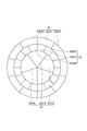
- FIG. 2 is a plan view showing an example of a layout of a plurality of heaters in the electrostatic chuck.
- the electrostatic chuck 18 has a plurality of zones Z1, Z2, and Z3 defined when the electrostatic chuck 18 is viewed in the vertical direction. These zones Z1 to Z3 are concentric zones. That is, the zone Z1 is a circular zone including the center of the electrostatic chuck 18, the zone Z2 is a substantially annular zone surrounding the zone Z1, and the zone Z3 is a substantially annular zone surrounding the zone Z2.
- zones Z1 to Z3 Multiple zones are defined in zones Z1 to Z3. That is, a plurality of segments are defined in the electrostatic chuck 18.
- segments are defined so as to divide the zone Z1 into L pieces in the circumferential direction, and the respective segments are SG11 to SG1L.
- segments are defined so as to divide the zone Z2 into M pieces in the circumferential direction, and the respective segments are designated SG21 to SG2M.
- segments are defined so as to divide the zone Z3 into N pieces in the circumferential direction, and the respective segments are SG31 to SG3N.
- the plurality of heaters HT are respectively arranged in the plurality of segments.
- the plurality of heaters HT are heating resistors having the same resistance value per unit length. Further, as shown in FIG. 2, the plurality of segments include segments having different areas. Therefore, the plurality of heaters HT include heaters having different resistance values. Electric power is supplied to the plurality of heaters HT by the power feeding device PS shown in FIG.
- the zones and segments defined in the electrostatic chuck 18 are not limited to the form shown in FIG.
- a plurality of segments defined by grid-like boundaries may be defined in the electrostatic chuck 18, or a plurality of segments that concentrically divide a region in the electrostatic chuck 18 may be defined.
- a larger number of zones than the number of zones shown in FIG. 2 may be defined, and the number of segments in each zone may be larger or smaller than the number of segments shown in FIG.
- a focus ring FR is provided on the upper surface of the base 20 and around the electrostatic chuck 18.
- the focus ring FR is provided in order to improve the uniformity of plasma processing.
- the focus ring FR is made of a material appropriately selected according to the plasma processing to be performed, and can be made of, for example, silicon or quartz.
- a coolant channel 24 is formed inside the base 20. Refrigerant is supplied to the refrigerant flow path 24 from a chiller unit provided outside the processing container 12 via a pipe 26a. The refrigerant supplied to the refrigerant flow path 24 returns to the chiller unit via the pipe 26b.
- the upper electrode 30 is provided in the processing container 12.
- the upper electrode 30 is disposed above the mounting table 16 so as to face the base 20, and the base 20 and the upper electrode 30 are provided substantially parallel to each other.
- the upper electrode 30 is supported on the upper part of the processing container 12 through an insulating shielding member 32.
- the upper electrode 30 can include an electrode plate 34 and an electrode support 36.
- the electrode plate 34 faces the processing space S and provides a plurality of gas discharge holes 34a.
- the electrode plate 34 can be made of a low resistance conductor or semiconductor with little Joule heat.
- the electrode support 36 supports the electrode plate 34 in a detachable manner and can be made of a conductive material such as aluminum.
- the electrode support 36 may have a water cooling structure.
- a gas diffusion chamber 36 a is provided inside the electrode support 36.
- a plurality of gas flow holes 36b communicating with the gas discharge holes 34a extend downward from the gas diffusion chamber 36a.
- the electrode support 36 is formed with a gas introduction port 36c for introducing a processing gas to the gas diffusion chamber 36a, and a gas supply pipe 38 is connected to the gas introduction port 36c.
- a gas source group 40 is connected to the gas supply pipe 38 via a valve group 42 and a flow rate controller group 44.
- the valve group 42 has a plurality of on-off valves
- the flow rate controller group 44 has a plurality of flow rate controllers such as a mass flow controller.
- the gas source group 40 includes gas sources for a plurality of types of gases necessary for plasma processing.
- the plurality of gas sources of the gas source group 40 are connected to the gas supply pipe 38 via corresponding open / close valves and corresponding mass flow controllers.
- one or more gases from one or more gas sources selected from the plurality of gas sources in the gas source group 40 are supplied to the gas supply pipe 38.
- the gas supplied to the gas supply pipe 38 reaches the gas diffusion chamber 36a and is discharged into the processing space S through the gas flow hole 36b and the gas discharge hole 34a.
- the plasma processing apparatus 10 may further include a ground conductor 12a.
- the ground conductor 12 a is a substantially cylindrical ground conductor, and is provided so as to extend above the height position of the upper electrode 30 from the side wall of the processing container 12.
- a deposition shield 46 is detachably provided along the inner wall of the processing container 12.
- the deposition shield 46 is also provided on the outer periphery of the support portion 14.
- the deposition shield 46 prevents the etching byproduct (depot) from adhering to the processing container 12 and can be configured by coating an aluminum material with ceramics such as Y 2 O 3 .
- an exhaust plate 48 is provided between the support portion 14 and the inner wall of the processing container 12.
- the exhaust plate 48 can be configured by, for example, coating an aluminum material with ceramics such as Y 2 O 3 .
- the processing vessel 12 is provided with an exhaust port 12e.
- An exhaust device 50 is connected to the exhaust port 12e via an exhaust pipe 52.
- the exhaust device 50 includes a vacuum pump such as a turbo molecular pump, and can reduce the pressure in the processing container 12 to a desired degree of vacuum.
- a loading / unloading port 12 g for the wafer W is provided on the side wall of the processing container 12, and the loading / unloading port 12 g can be opened and closed by a gate valve 54.
- the plasma processing apparatus 10 may further include a control unit Cnt.
- the control unit Cnt is a computer including a processor, a storage unit, an input device, a display device, and the like, and controls each unit of the plasma processing apparatus 10.
- an operator can perform a command input operation and the like to manage the plasma processing apparatus 10 using the input device, and the operating status of the plasma processing apparatus 10 is visualized by the display device. Can be displayed.
- the storage unit of the control unit Cnt causes the respective components of the plasma processing apparatus 10 to execute processes according to a control program for controlling various processes executed by the plasma processing apparatus 10 by the processor and processing conditions.
- a program for processing, that is, a processing recipe is stored.
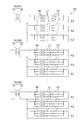
- FIG. 3 is a diagram illustrating a power supply apparatus according to an embodiment.
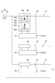
- FIG. 4 is a diagram illustrating the configuration of the SSR 80 together with a part of the power supply apparatus according to the embodiment.
- the power feeding device PS includes a plurality of transformers 70 and a plurality of zero-cross control type solid state relays 80 (hereinafter referred to as “SSR 80”).
- SSR 80 Each of the plurality of transformers 70 includes a primary coil 71 and a secondary coil 72.
- the primary coil 71 is electrically connected to an AC power source, for example, a three-phase AC power source.
- Each of the SSRs 80 is provided between one corresponding heater HT among the plurality of heaters HT and the secondary coil 72 of one corresponding transformer among the plurality of transformers 70.
- Each first terminal of the plurality of heaters HT is connected to a corresponding one SSR 80 via a first wiring L1.
- the SSR 80 is connected to the secondary coil 72 of the corresponding transformer 70.
- nine SSRs 80 are connected to the secondary coil 72 of one transformer 70.
- the heater HT connected to one transformer 70 via the SSR 80 can be arbitrarily set.
- the SSR 80 includes an input circuit 80a, a photocoupler 80b, a zero cross circuit 80c, a trigger circuit 80d, a triac 80e, and a snubber circuit 80f.
- a temperature control unit 82 is connected to the input circuit 80a.
- the temperature control unit 82 provides a control signal for adjusting a period during which the heater HT and the transformer 70 are electrically connected to the input circuit 80a.
- the temperature control unit 82 receives a signal transmitted from the control unit Cnt to generate heat with the amount of heat generated according to the recipe, and adjusts the period during which the heater HT and the transformer 70 are conducted according to this signal.
- a control signal for generating The temperature control unit 82 receives the current value measured by the current monitor 84 and generates a control signal according to the current value.
- the input circuit 80a outputs an input signal sent to the light emitting element of the photocoupler 80b in response to the control signal from the temperature control unit 82.
- this input signal is turned on, the SSR 80 is turned on near zero voltage, and the heater HT and the transformer 70 are made conductive.
- the SSR 80 is turned off in the vicinity of the zero voltage, and current is not substantially supplied to the heater HT.
- FIG. 5 shows an example of a waveform of current generated by ON / OFF control by SSR.
- the waveform current indicated by the solid line indicates the current supplied to the heater HT
- the waveform indicated by the dotted line indicates that no current is supplied to the heater HT during the period when the SSR 80 is OFF.
- SSR 80 the conduction state of heater HT and transformer 70 is switched around zero voltage. Therefore, as shown in FIG. 5, the high frequency component is suppressed in the waveform of the generated current. Therefore, according to SSR 80, generation of high frequency noise can be suppressed.
- the SSR 80 can cope with high-speed and high-frequency switching of ON / OFF, and since it is a contactless relay, it has an advantage that there is no contact failure and there is no operation sound. Further, SSR 80 has an advantage that it is less expensive than thyristors.
- the plurality of heaters HT are arranged in parallel for each group including two or more heaters HT.
- the second terminals of two or more heaters HT constituting one group are electrically connected to one common wiring, that is, the second wiring L2.
- one or more second wirings L ⁇ b> 2 are connected to the secondary coil 72 of one transformer 70.
- each of the plurality of second wirings L2 shares the second terminal of the corresponding two or more heaters among the plurality of heaters HT and the secondary coil 72 of the corresponding transformer among the plurality of transformers 70. Connected.
- FIG. 1 the embodiment shown in FIG.
- the number of heaters HT commonly connected to one second wiring L2 is three, but the number of heaters HT commonly connected to one second wiring L2 is used. Can be set arbitrarily.
- the three second wirings L ⁇ b> 2 are connected to the secondary coil 72 of one transformer 70, but the second wiring L ⁇ b> 2 is connected to the secondary coil 72 of one transformer 70.
- the number of the two wirings L2 can be set arbitrarily.
- Each of the plurality of transformers 70 outputs a voltage obtained by stepping down the voltage on the primary side to the secondary side, that is, the secondary coil 72.
- a first example of the power feeding device PS will be considered.
- nine heaters HT are connected in parallel to each of a plurality of transformers 70, that is, a transformer 701, a transformer 702, and a transformer 703. .
- the resistance values of the nine heaters HT connected to one transformer are 45.5 ⁇ , 40.4 ⁇ , 22.5 ⁇ , 45.5 ⁇ , 40.4 ⁇ , 22.5 ⁇ , 45.5 ⁇ , 40. It shall be 4 ⁇ and 22.5 ⁇ .
- the transformer 701 is given a voltage from the R-phase S phase of the three-phase AC power supply, the transformer 702 is given a voltage from the S-phase T phase of the three-phase AC power supply, and the transformer 703 is given a three-phase voltage. It is assumed that a voltage is applied from the R phase-T phase of the phase AC power supply.
- the combined resistance value of the nine heaters HT connected to each transformer is 3.7 ⁇ .
- the maximum current is 46.8A. Further, when the voltage is lowered to 50 V by the transformer 70 (701, 702, 703), the maximum current becomes 23.4A. Therefore, the maximum amount of current can be reduced by adopting the transformer 70.
- the control resolution of the temperature control unit 82 that is, the control resolution of the heat generation amount of each heater HT can be improved with respect to the output resolution of the temperature control unit 82. Therefore, even if the heaters HT having different resistance values are connected in parallel to each transformer 70 as in the first example, it is possible to improve the resolution of temperature control by each heater HT. Further, since the power supply device PS is configured by the transformer 70 and the SSR 80, an inexpensive and small-sized power supply device PS is provided. Further, in a configuration having a plurality of heaters HT provided in a plurality of segments, it is possible to reduce current consumption.
- each of the nine heaters HT connected in parallel to one transformer have substantially the same resistance value.
- each of the nine heaters HT connected to the transformer 701 has a resistance value of 45.5 ⁇ .
- each of the nine heaters HT connected to the transformer 702 has a resistance value of 40.4 ⁇ .
- each of the nine heaters HT connected to the transformer 703 has a resistance value of 25.5 ⁇ .
- the area of the segment provided with each heater HT connected to the transformer 701 is 2800 mm 2
- the area of the segment provided with each heater HT connected to the transformer 702 is 2300 mm 2 .
- the transformer 701 is given a voltage from the R-phase S phase of the three-phase AC power supply
- the transformer 702 is given a voltage from the S-phase T phase of the three-phase AC power supply
- the transformer 703 is given a three-phase voltage. It is assumed that a voltage is applied from the R phase-T phase of the phase AC power supply. Further, the transformer 701 steps down the voltage to 100V, the transformer 702 steps down the voltage to 75V, and the transformer 703 steps down the voltage to 50V.
- the combined resistance value of the nine heaters HT connected to the transformer 701 is 5.1 ⁇
- the combined resistance value of the nine heaters HT connected to the transformer 702 is 4.5 ⁇
- the combined resistance value of the nine heaters HT connected to the vessel 703 is 2.5 ⁇ . Therefore, the current consumed in the R phase-S phase is 19.6 A, and the heat generation amount in the R phase-S phase is 1960.8 W. Further, the current consumed in the S-T phase is 19.8 A, and the calorific value in the S-T phase is 1253.1 W. In addition, the current consumed in the R phase and the T phase is 20.0 A, and the heat generation amount in the R phase and the T phase is 1000 W.
- the heat generation amount per unit area of the segment where each heater HT connected to the transformer 701 is provided that is, the heat generation density is 0.08 W / mm 2 .
- the heat generation density of the segment provided with each heater HT connected to the transformer 702 is 0.06 W / mm 2 .
- the heat generation density of the segment provided with each heater HT connected to the transformer 703 is 0.09 W / mm 2 .
- the resolution of the temperature control will be examined taking the heater HT connected to the transformer 701 of the second example as an example.
- the resistance value of the nine heaters HT connected to the transformer 701 is 45.5 ⁇ , and the area of the segment in which each heater HT is provided is 2800 mm 2 .
- the output resolution of the temperature control unit 82 is 0.1%.
- the output resolution of the temperature control unit 82 means that the power supplied to the heater HT can be controlled in units of 0.1%.
- the amount of heat generated to raise the temperature of each segment by 1 ° C. is calculated by segment area ⁇ heat flux.
- this examination confirms that high temperature control resolution can be realized by the power supply apparatus PS. Further, by increasing the output resolution of the temperature control unit 82, for example, 0.05%, a higher temperature control resolution can be obtained.
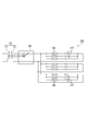
- FIG. 6 is a diagram illustrating a part of a power feeding apparatus according to another embodiment.
- the power feeding device PS includes a switch 90 between each transformer 70 and the SSR 80. That is, in the power supply device PS of another embodiment, a plurality of switches 90 are connected to each of the plurality of transformers.
- the switch 90 adjusts the output voltage on the secondary side of the transformer 70 by changing the transformation ratio of the corresponding transformer 70.
- the switch 90 may be configured as a relay circuit that selects any of the plurality of taps of the transformer 70 and connects to the selected tap.
- the switch 90 can switch the tap to be selected by the control by the control unit Cnt described above.
- FIG. 7 is a flowchart showing an embodiment of a method for operating the plasma processing apparatus 10 including the power supply apparatus shown in FIG.
- the operation method shown in FIG. 7 includes a first step ST1 and a second step ST2.
- 1st process ST1 the several switch 90 connected to each of the some transformer 70 is controlled, and the transformation ratio of these transformers 70 is set.
- the control of the plurality of switches 90 in the first step ST1 can be executed by the first control by the control unit Cnt.
- the plurality of switches 90 are controlled, and the transformation ratios of these transformers 70 are set to a transformation ratio higher than the transformation ratio of the plurality of transformers 70 set in the first step ST1.
- the control of the plurality of switches 90 in the second step ST2 can be executed by the second control by the control unit Cnt.
- a voltage lower than the voltage on the secondary side of the first step ST2 is output to the secondary side of the transformer 70. Therefore, the amount of current supplied to the corresponding heater HT connected to the transformer 70 is reduced.
- the resolution of temperature control can be increased.
- the first step ST1 since a large current can be supplied to the heater HT, rapid heating becomes possible.
- the temperature in the second process is higher than the temperature of the wafer W in the first process. It can be used when the temperature of the wafer W needs to be raised rapidly.
- the output voltage on the secondary side of the transformer 70 is increased by switching the connection destination to a tap that can obtain a low transformation ratio, and the amount of current supplied to the heater HT is increased. The temperature of the wafer W can be raised rapidly.
- the output voltage on the secondary side of the transformer 70 is lowered and supplied to the heater HT by switching the connection destination to a tap capable of obtaining a high transformation ratio.
- the temperature of the mounting table 16 and the wafer W by the heater HT can be controlled with high accuracy.
- the plasma processing apparatus of the above-described embodiment is a capacitively coupled plasma processing apparatus, but the plasma processing apparatus may be an arbitrary type of plasma processing apparatus.
- the plasma processing apparatus may be an inductively coupled plasma processing apparatus or a plasma processing apparatus that uses surface waves such as microwaves as a plasma source.
- SYMBOLS 10 Plasma processing apparatus, 12 ... Processing container, 16 ... Mounting stand, 18 ... Electrostatic chuck, 20 ... Base, HT ... Heater, PS ... Feeding device, 70 ... Transformer, 71 ... Primary coil, 72 ... Secondary Coil, 80 ... solid state relay, 82 ... temperature control unit, 90 ... switch, Cnt ... control unit.
Landscapes
- Engineering & Computer Science (AREA)
- Physics & Mathematics (AREA)
- Plasma & Fusion (AREA)
- Chemical & Material Sciences (AREA)
- Analytical Chemistry (AREA)
- Spectroscopy & Molecular Physics (AREA)
- Electromagnetism (AREA)
- Mechanical Engineering (AREA)
- General Engineering & Computer Science (AREA)
- Ceramic Engineering (AREA)
- Inorganic Chemistry (AREA)
- Drying Of Semiconductors (AREA)
- Plasma Technology (AREA)
- Control Of Resistance Heating (AREA)
- Container, Conveyance, Adherence, Positioning, Of Wafer (AREA)
Abstract
Description
Claims (8)
- 被処理体に対してプラズマ処理を行うためのプラズマ処理装置であって、
処理容器と、
前記処理容器内に設けられた載置台と、
前記載置台内に設けられた複数のヒータと、
前記複数のヒータに電力を供給する給電装置と、
を備え、
前記給電装置は、
交流電源からの電圧を降圧するように構成された複数の変圧器であり、各々が、該交流電源に接続された一次コイル、及び二次コイルを有する、該複数の変圧器と、
各々が、前記複数のヒータのうち対応の一つのヒータと前記複数の変圧器のうち対応の一つの変圧器の二次コイルとの間に設けられた複数のゼロクロス制御型のソリッドステートリレーと、
を有する、プラズマ処理装置。 - 前記複数のヒータの第1端子と前記複数のゼロクロス制御型のソリッドステートリレーとを個別に接続する複数の第1配線と、
各々が、前記複数のヒータのうち対応の二以上のヒータの第2端子と前記複数の変圧器のうち対応の一つの変圧器の二次コイルとを共通に接続する複数の第2配線と、
を更に備える、請求項1に記載のプラズマ処理装置。 - 前記複数の第2配線のうち共通の第2配線に接続された二以上のヒータは、同一の抵抗値を有する、請求項2に記載のプラズマ処理装置。
- 前記給電装置は、前記複数の変圧器の変圧比を変更する複数の切替器を更に有する、
請求項1~3の何れか一項に記載のプラズマ処理装置。 - 前記複数の切替器を制御する制御部を更に備え、
前記制御部は、
前記複数の切替器を制御して、前記複数の変圧器の変圧比を設定する第1制御と、
前記複数の切替器を制御して、前記第1制御において設定された前記複数の変圧器の変圧比よりも高い変圧比に前記複数の変圧器の変圧比を設定する第2制御と、
を実行する、請求項4に記載のプラズマ処理装置。 - 請求項4に記載されたプラズマ処理装置の運用方法であって、
前記複数の切替器を制御して、前記複数の変圧器の変圧比を設定する第1工程と、
前記複数の切替器を制御して、前記第1工程において設定された前記複数の変圧器の変圧比よりも高い変圧比に前記複数の変圧器の変圧比を設定する第2工程と、
を含む運用方法。 - プラズマ処理装置の載置台内に設けられた複数のヒータに電力を供給するための給電装置であって、
交流電源からの電圧を降圧するように構成された複数の変圧器であり、各々が、該交流電源に接続された一次コイル、及び二次コイルを有する、該複数の変圧器と、
各々が、前記複数のヒータのうち対応の一つのヒータと前記複数の変圧器のうち対応の一つの変圧器の二次コイルとの間に設けられた複数のゼロクロス制御型のソリッドステートリレーと、
を備える給電装置。 - 前記複数の変圧器の変圧比を変更する複数の切替器を更に備える、請求項7に記載の給電装置。
Priority Applications (3)
| Application Number | Priority Date | Filing Date | Title |
|---|---|---|---|
| CN201580024624.XA CN106463390B (zh) | 2014-06-11 | 2015-06-01 | 等离子体处理装置及等离子体处理装置的运用方法 |
| KR1020167031236A KR102363557B1 (ko) | 2014-06-11 | 2015-06-01 | 플라즈마 처리 장치, 플라즈마 처리 장치의 운용 방법 및 급전 장치 |
| US15/309,399 US10699883B2 (en) | 2014-06-11 | 2015-06-01 | Plasma processing apparatus, method of operating plasma processing apparatus, and power supply device |
Applications Claiming Priority (2)
| Application Number | Priority Date | Filing Date | Title |
|---|---|---|---|
| JP2014-120251 | 2014-06-11 | ||
| JP2014120251A JP6265841B2 (ja) | 2014-06-11 | 2014-06-11 | プラズマ処理装置及びプラズマ処理装置の運用方法 |
Publications (1)
| Publication Number | Publication Date |
|---|---|
| WO2015190336A1 true WO2015190336A1 (ja) | 2015-12-17 |
Family
ID=54833434
Family Applications (1)
| Application Number | Title | Priority Date | Filing Date |
|---|---|---|---|
| PCT/JP2015/065771 Ceased WO2015190336A1 (ja) | 2014-06-11 | 2015-06-01 | プラズマ処理装置、プラズマ処理装置の運用方法、及び給電装置 |
Country Status (6)
| Country | Link |
|---|---|
| US (1) | US10699883B2 (ja) |
| JP (1) | JP6265841B2 (ja) |
| KR (1) | KR102363557B1 (ja) |
| CN (1) | CN106463390B (ja) |
| TW (1) | TWI672726B (ja) |
| WO (1) | WO2015190336A1 (ja) |
Cited By (1)
| Publication number | Priority date | Publication date | Assignee | Title |
|---|---|---|---|---|
| JP2022058827A (ja) * | 2016-05-31 | 2022-04-12 | ラム・リサーチ・アーゲー | ウエハ形状の物品を処理するための方法および装置 |
Families Citing this family (19)
| Publication number | Priority date | Publication date | Assignee | Title |
|---|---|---|---|---|
| JP2017188238A (ja) * | 2016-04-04 | 2017-10-12 | 住友電気工業株式会社 | マトリックスヒータ |
| JP2018063974A (ja) | 2016-10-11 | 2018-04-19 | 東京エレクトロン株式会社 | 温度制御装置、温度制御方法、および載置台 |
| JP6819531B2 (ja) | 2017-09-28 | 2021-01-27 | トヨタ自動車株式会社 | 金属皮膜の成膜方法および金属皮膜の成膜装置 |
| JP6593413B2 (ja) * | 2017-10-10 | 2019-10-23 | 住友電気工業株式会社 | ウエハ加熱用ヒータユニット |
| JP6593414B2 (ja) * | 2017-10-10 | 2019-10-23 | 住友電気工業株式会社 | ウエハ加熱用ヒータユニット |
| KR20190053941A (ko) * | 2017-10-10 | 2019-05-20 | 스미토모덴키고교가부시키가이샤 | 웨이퍼 가열용 히터 유닛 |
| JP6593415B2 (ja) * | 2017-10-10 | 2019-10-23 | 住友電気工業株式会社 | ウエハ加熱用ヒータユニット |
| CN110275556B (zh) * | 2018-03-14 | 2022-04-22 | 北京北方华创微电子装备有限公司 | 静电卡盘的温度控制方法、系统及半导体处理设备 |
| KR102161130B1 (ko) * | 2018-09-27 | 2020-10-05 | 세메스 주식회사 | 기판 처리 장치 및 기판 처리 방법 |
| JP7299756B2 (ja) * | 2019-05-24 | 2023-06-28 | 日本特殊陶業株式会社 | 保持装置 |
| JP7292115B2 (ja) * | 2019-06-07 | 2023-06-16 | 東京エレクトロン株式会社 | 温度調整装置及び温度制御方法。 |
| JP7071946B2 (ja) * | 2019-06-21 | 2022-05-19 | 東京エレクトロン株式会社 | プラズマ処理装置 |
| CN111795409B (zh) * | 2020-08-03 | 2025-08-05 | 深圳国爱全电化智慧科技有限公司 | 一种单个电极可控的等离子体灶 |
| JP7616877B2 (ja) * | 2020-12-14 | 2025-01-17 | ソニーセミコンダクタソリューションズ株式会社 | プロービング装置 |
| US12317378B2 (en) * | 2021-02-04 | 2025-05-27 | Applied Materials, Inc. | Multi-zone heater control for wafer processing equipment |
| US12211677B2 (en) * | 2021-07-21 | 2025-01-28 | Applied Materials, Inc. | Uniformity control for plasma processing |
| JPWO2024150693A1 (ja) * | 2023-01-10 | 2024-07-18 | ||
| JP2025132352A (ja) * | 2024-02-29 | 2025-09-10 | 株式会社Screenホールディングス | 基板処理装置および基板処理方法 |
| JP2026038380A (ja) * | 2024-08-23 | 2026-03-06 | 日本特殊陶業株式会社 | 保持装置 |
Citations (8)
| Publication number | Priority date | Publication date | Assignee | Title |
|---|---|---|---|---|
| JPS60246416A (ja) * | 1984-05-22 | 1985-12-06 | Mitsubishi Electric Corp | 加熱電源装置 |
| JPH03165483A (ja) * | 1989-11-24 | 1991-07-17 | Tokyo Erekutoron Kyushu Kk | 加熱装置 |
| JPH06208315A (ja) * | 1993-01-08 | 1994-07-26 | Fuji Xerox Co Ltd | 画像形成装置の定着装置 |
| JPH07183281A (ja) * | 1993-12-24 | 1995-07-21 | Tokyo Electron Ltd | 処理装置 |
| JP2004241745A (ja) * | 2003-02-10 | 2004-08-26 | Hitachi Kokusai Electric Inc | 基板処理装置 |
| JP2004533718A (ja) * | 2001-04-30 | 2004-11-04 | ラム リサーチ コーポレイション | ワーク支持体の表面を横切る空間温度分布を制御する方法および装置 |
| JP2009231247A (ja) * | 2008-03-25 | 2009-10-08 | Tokyo Electron Ltd | プラズマ処理装置及び高周波電力の供給方法 |
| JP2011187404A (ja) * | 2010-03-11 | 2011-09-22 | Omron Corp | 温度制御システム |
Family Cites Families (9)
| Publication number | Priority date | Publication date | Assignee | Title |
|---|---|---|---|---|
| JPS5222850B2 (ja) | 1975-02-15 | 1977-06-20 | ||
| US6847014B1 (en) * | 2001-04-30 | 2005-01-25 | Lam Research Corporation | Method and apparatus for controlling the spatial temperature distribution across the surface of a workpiece support |
| US7501605B2 (en) | 2006-08-29 | 2009-03-10 | Lam Research Corporation | Method of tuning thermal conductivity of electrostatic chuck support assembly |
| CN102044327A (zh) * | 2009-10-19 | 2011-05-04 | 富士电子工业株式会社 | 高频感应加热用薄型变压器 |
| JP5592098B2 (ja) * | 2009-10-27 | 2014-09-17 | 東京エレクトロン株式会社 | プラズマ処理装置及びプラズマ処理方法 |
| JP5643062B2 (ja) * | 2009-11-24 | 2014-12-17 | 東京エレクトロン株式会社 | プラズマ処理装置 |
| JP2011187637A (ja) | 2010-03-08 | 2011-09-22 | Hitachi Kokusai Electric Inc | 半導体製造装置 |
| JP2014082463A (ja) * | 2012-09-27 | 2014-05-08 | Hitachi Kokusai Electric Inc | 基板処理装置、蓋体及び半導体装置の製造方法 |
| JP6332746B2 (ja) * | 2013-09-20 | 2018-05-30 | 株式会社日立国際電気 | 基板処理装置、半導体装置の製造方法及びプログラム |
-
2014
- 2014-06-11 JP JP2014120251A patent/JP6265841B2/ja active Active
-
2015
- 2015-06-01 WO PCT/JP2015/065771 patent/WO2015190336A1/ja not_active Ceased
- 2015-06-01 KR KR1020167031236A patent/KR102363557B1/ko active Active
- 2015-06-01 CN CN201580024624.XA patent/CN106463390B/zh active Active
- 2015-06-01 US US15/309,399 patent/US10699883B2/en active Active
- 2015-06-09 TW TW104118549A patent/TWI672726B/zh active
Patent Citations (8)
| Publication number | Priority date | Publication date | Assignee | Title |
|---|---|---|---|---|
| JPS60246416A (ja) * | 1984-05-22 | 1985-12-06 | Mitsubishi Electric Corp | 加熱電源装置 |
| JPH03165483A (ja) * | 1989-11-24 | 1991-07-17 | Tokyo Erekutoron Kyushu Kk | 加熱装置 |
| JPH06208315A (ja) * | 1993-01-08 | 1994-07-26 | Fuji Xerox Co Ltd | 画像形成装置の定着装置 |
| JPH07183281A (ja) * | 1993-12-24 | 1995-07-21 | Tokyo Electron Ltd | 処理装置 |
| JP2004533718A (ja) * | 2001-04-30 | 2004-11-04 | ラム リサーチ コーポレイション | ワーク支持体の表面を横切る空間温度分布を制御する方法および装置 |
| JP2004241745A (ja) * | 2003-02-10 | 2004-08-26 | Hitachi Kokusai Electric Inc | 基板処理装置 |
| JP2009231247A (ja) * | 2008-03-25 | 2009-10-08 | Tokyo Electron Ltd | プラズマ処理装置及び高周波電力の供給方法 |
| JP2011187404A (ja) * | 2010-03-11 | 2011-09-22 | Omron Corp | 温度制御システム |
Cited By (2)
| Publication number | Priority date | Publication date | Assignee | Title |
|---|---|---|---|---|
| JP2022058827A (ja) * | 2016-05-31 | 2022-04-12 | ラム・リサーチ・アーゲー | ウエハ形状の物品を処理するための方法および装置 |
| JP7324323B2 (ja) | 2016-05-31 | 2023-08-09 | ラム・リサーチ・アーゲー | ウエハ形状の物品を処理するための方法および装置 |
Also Published As
| Publication number | Publication date |
|---|---|
| JP2016001638A (ja) | 2016-01-07 |
| KR102363557B1 (ko) | 2022-02-17 |
| JP6265841B2 (ja) | 2018-01-24 |
| CN106463390B (zh) | 2019-08-06 |
| TWI672726B (zh) | 2019-09-21 |
| US10699883B2 (en) | 2020-06-30 |
| CN106463390A (zh) | 2017-02-22 |
| US20170110297A1 (en) | 2017-04-20 |
| KR20170009852A (ko) | 2017-01-25 |
| TW201611086A (zh) | 2016-03-16 |
Similar Documents
| Publication | Publication Date | Title |
|---|---|---|
| JP6265841B2 (ja) | プラズマ処理装置及びプラズマ処理装置の運用方法 | |
| US11373884B2 (en) | Placing table and plasma treatment apparatus | |
| JP5657262B2 (ja) | プラズマ処理装置 | |
| JP7158131B2 (ja) | ステージ及びプラズマ処理装置 | |
| JP6442296B2 (ja) | 載置台及びプラズマ処理装置 | |
| JP6100672B2 (ja) | 温度制御機構、温度制御方法及び基板処理装置 | |
| TWI651798B (zh) | 載置台及電漿處理裝置 | |
| US20180190501A1 (en) | Plasma processing apparatus | |
| JP2018117024A (ja) | プラズマ処理装置 | |
| TW201838028A (zh) | 電漿處理裝置 | |
| CN112687511B (zh) | 等离子体处理装置及等离子体处理方法 | |
| JP2018085372A (ja) | 載置台及びプラズマ処理装置 | |
| JP2019176030A (ja) | プラズマ処理装置 | |
| KR20200115228A (ko) | 플라즈마 처리 장치 | |
| US10593522B2 (en) | Electrostatic chuck, placing table and plasma processing apparatus | |
| JP2021052032A (ja) | 誘電体部品、構造体及び基板処理装置 |
Legal Events
| Date | Code | Title | Description |
|---|---|---|---|
| 121 | Ep: the epo has been informed by wipo that ep was designated in this application |
Ref document number: 15807230 Country of ref document: EP Kind code of ref document: A1 |
|
| WWE | Wipo information: entry into national phase |
Ref document number: 15309399 Country of ref document: US |
|
| ENP | Entry into the national phase |
Ref document number: 20167031236 Country of ref document: KR Kind code of ref document: A |
|
| NENP | Non-entry into the national phase |
Ref country code: DE |
|
| 122 | Ep: pct application non-entry in european phase |
Ref document number: 15807230 Country of ref document: EP Kind code of ref document: A1 |