WO2015190216A1 - デジタルフィルタ - Google Patents
デジタルフィルタ Download PDFInfo
- Publication number
- WO2015190216A1 WO2015190216A1 PCT/JP2015/063979 JP2015063979W WO2015190216A1 WO 2015190216 A1 WO2015190216 A1 WO 2015190216A1 JP 2015063979 W JP2015063979 W JP 2015063979W WO 2015190216 A1 WO2015190216 A1 WO 2015190216A1
- Authority
- WO
- WIPO (PCT)
- Prior art keywords
- stage
- difference calculation
- calculation unit
- data
- unit
- Prior art date
- Legal status (The legal status is an assumption and is not a legal conclusion. Google has not performed a legal analysis and makes no representation as to the accuracy of the status listed.)
- Ceased
Links
Images




Classifications
-
- H—ELECTRICITY
- H03—ELECTRONIC CIRCUITRY
- H03H—IMPEDANCE NETWORKS, e.g. RESONANT CIRCUITS; RESONATORS
- H03H17/00—Networks using digital techniques
- H03H17/02—Frequency selective networks
- H03H17/0248—Filters characterised by a particular frequency response or filtering method
- H03H17/025—Notch filters
-
- H—ELECTRICITY
- H03—ELECTRONIC CIRCUITRY
- H03H—IMPEDANCE NETWORKS, e.g. RESONANT CIRCUITS; RESONATORS
- H03H17/00—Networks using digital techniques
- H03H17/02—Frequency selective networks
- H03H17/0248—Filters characterised by a particular frequency response or filtering method
- H03H17/0282—Sinc or gaussian filters
-
- H—ELECTRICITY
- H03—ELECTRONIC CIRCUITRY
- H03H—IMPEDANCE NETWORKS, e.g. RESONANT CIRCUITS; RESONATORS
- H03H17/00—Networks using digital techniques
- H03H17/02—Frequency selective networks
- H03H17/0283—Filters characterised by the filter structure
- H03H17/0286—Combinations of filter structures
-
- H—ELECTRICITY
- H03—ELECTRONIC CIRCUITRY
- H03H—IMPEDANCE NETWORKS, e.g. RESONANT CIRCUITS; RESONATORS
- H03H17/00—Networks using digital techniques
- H03H17/02—Frequency selective networks
- H03H17/06—Non-recursive filters
- H03H17/0621—Non-recursive filters with input-sampling frequency and output-delivery frequency which differ, e.g. extrapolation; Anti-aliasing
- H03H17/0635—Non-recursive filters with input-sampling frequency and output-delivery frequency which differ, e.g. extrapolation; Anti-aliasing characterized by the ratio between the input-sampling and output-delivery frequencies
- H03H17/0671—Cascaded integrator-comb [CIC] filters
-
- H—ELECTRICITY
- H03—ELECTRONIC CIRCUITRY
- H03M—CODING; DECODING; CODE CONVERSION IN GENERAL
- H03M3/00—Conversion of analogue values to or from differential modulation
- H03M3/02—Delta modulation, i.e. one-bit differential modulation
-
- H—ELECTRICITY
- H03—ELECTRONIC CIRCUITRY
- H03M—CODING; DECODING; CODE CONVERSION IN GENERAL
- H03M3/00—Conversion of analogue values to or from differential modulation
- H03M3/30—Delta-sigma modulation
- H03M3/458—Analogue/digital converters using delta-sigma modulation as an intermediate step
- H03M3/462—Details relating to the decimation process
Definitions
- the present invention relates to a digital filter, and more particularly to a digital filter combining a SINC filter and a notch filter.
- a SINC filter is well known as a decimation filter used in a ⁇ AD converter.
- the SINC filter can be expressed by a transfer function of (1-z ⁇ N ) / (1-z ⁇ 1 ).
- the order of the subsequent decimation filter (SINC filter) needs to be higher than the order of the ⁇ modulator. It is well known that there is.
- the SINC filter As the SINC filter, a third-order filter is required as shown in FIG. If this SINC filter is expressed by a transfer function, ⁇ (1 ⁇ z ⁇ N ) / (1 ⁇ z ⁇ 1 ) ⁇ ⁇ 3.
- this SINC filter is also possible to separate the integration calculation part constituting the denominator part of the transfer function and the difference calculation part constituting the numerator part of the transfer function, and to place the difference calculation part after down-sampling at a frequency of 1 / N.
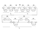
- the SINC filter has a configuration in which the integration calculator 100 connected in three stages and the difference calculator 101 connected in three stages are connected by a frequency converter 102.
- the integration calculation unit 100 operates at the sampling frequency f S
- a filter for removing 50 Hz / 60 Hz which is a commercial frequency is often required.
- a filter for removing a specific frequency such as 50 Hz / 60 Hz
- a band limit filter and a notch filter are known. These filters can be realized by an analog circuit, but a notch filter can be realized by a digital circuit as shown in FIGS.
- the notch filter that removes the 50 Hz component included in the input data includes a difference calculation unit 200 and an integration calculation unit 201 as shown in FIG.
- the delay unit constituting the difference calculation unit 200 is configured in a two-stage cascade connection so as to obtain the difference from the data two samples before.
- the notch filter that removes the 60 Hz component included in the input data includes a difference calculation unit 300 and an integration calculation unit 301 as shown in FIG.
- the delay unit configuring the difference calculation unit 300 is configured in a five-stage cascade connection so as to obtain the difference from the data before 5 samples, The frequency component can be removed.
- the signal lines have a plurality of bit widths.
- the bit width must be selected so as not to cause internal saturation.
- the bit width depends on the frequency ratio N for downsampling, and K ⁇ log 2 (N) +1 [bit] is required (see “JCCandy and GCTemes,“ Oversampling Delta-Sigma Data Converters ”, IEEE Press, p. 1-29, 1991 ”).
- N 256, 25 bits are required. Therefore, a register corresponding to the bit width is required.
- the digital filter requires a register corresponding to the bit width of the data, but the circuit scale of the adder circuit and the subtractor circuit with the data in the register increases as the bit width increases.
- the output of a digital filter is often 16 to 24 bits. For this reason, the increase in circuit scale becomes significant.
- the chip area is increased, so that an economic burden has been imposed by increasing the chip unit price.
- the present invention has been made to solve the above-described problems, and an object thereof is to reduce the circuit scale of a digital filter combining a SINC filter and a notch filter.
- the digital filter of the present invention operates with a clock having the same sampling frequency f S as the sampling frequency of the input data, and integrates the multi-stage cascade connection configuration for integrating the input data for each sample, and the multi-stage cascade connection configuration
- a multi-stage cascade connection configuration that operates with a clock of f D and subtracts data one sample before from the data input from the frequency converter or a first difference calculator of one stage and a clock with a sampling frequency f D
- the first difference calculator of the last stage or the first difference calculator of the first stage of the first difference calculators of the multiple-stage cascade connection configuration It is characterized in that and a second difference calculator for specific frequency removal subtracting a plurality of samples before the data from the data input.
- the digital filter includes an integration calculation unit having a multi-stage cascade connection configuration, a frequency conversion unit, a multi-stage cascade connection configuration or a first difference calculation unit of one stage, and a second difference calculation unit.
- an integration calculation unit having a multi-stage cascade connection configuration, a frequency conversion unit, a multi-stage cascade connection configuration or a first difference calculation unit of one stage, and a second difference calculation unit.
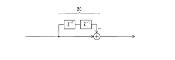
- FIG. 1A and 1B are diagrams illustrating the principle of combining a difference calculation unit of a SINC filter and an integration calculation unit of a notch filter in the present invention.
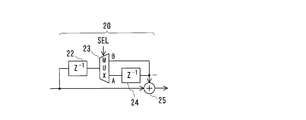
- FIG. 2 is a diagram for explaining the principle of switching between valid / invalid of the notch filter in the present invention.
- FIG. 3 is a block diagram showing the configuration of the digital filter according to the first embodiment of the present invention.
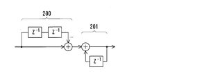
- 4A, 4B, and 4C are diagrams for explaining the principle of simplifying the configuration in the second embodiment of the present invention.
- FIG. 5 is a block diagram showing the configuration of the digital filter according to the second embodiment of the present invention.
- FIG. 6 is a block diagram showing a digital filter integration calculation and frequency converter configuration according to the second embodiment of the present invention.
- FIG. 7 is a block diagram showing a configuration of a conventional SINC filter.
- FIG. 8 is a block diagram showing the configuration of a conventional notch filter that removes 50 Hz.
- FIG. 9 is a block diagram showing the configuration of a conventional notch filter that removes 60 Hz.
- FIG. 10 is a block diagram showing a configuration in which a SINC filter and a notch filter are combined.
- FIG. 1A shows a difference calculation unit 11 of the SINC filter, and a notch filter including a difference calculation unit 20 and an integration calculation unit 21 connected to the subsequent stage of the SINC filter.
- the circuit scale of the digital filter is reduced by combining (cancelling) the difference calculation unit 11 of the SINC filter and the integration calculation unit 21 of the notch filter.
- FIG. 1B by combining the difference calculation unit 11 and the integration calculation unit 21, only the difference calculation unit 20 of the 50 Hz removal notch filter remains.
- the cut-off frequency of the filter can be changed depending on the sampling frequency, but the configuration of the notch filter is determined by the commercial frequency and thus is determined by the absolute value of the frequency. Therefore, the sampling frequency is uniquely determined by the hardware configuration.
- the delay unit 22 and the delay unit 24 are connected in series, so that 20 in FIG. 2 functions as a difference calculation unit of the 50 Hz removal notch filter.
- the delay unit 24 is out of the signal path, so that it does not function as a notch filter, and 20 in FIG. 2 functions as a difference calculation unit of the SINC filter.
- FIG. 3 is a block diagram showing the configuration of the digital filter according to the first embodiment of the present invention.
- the digital filter of the present embodiment operates with a clock having the same sampling frequency f S as the sampling frequency of data input to the digital filter, and has a multistage cascade connection configuration that integrates input data for each sample.
- Each integration calculation unit 10 adds the data of the sampling frequency f S input to the integration calculation unit 10 and the integration result of one sample before, and the integration result output from the addition unit 13 for one sample.
- the delay unit 14 is input to the adder unit 13 after being delayed by the amount corresponding to the clock frequency of the sampling frequency f S.
- each integration calculation unit 10 integrates the data input to the integration calculation unit 10 for each clock of the sampling frequency f S.
- the number of stages i of the integration calculation unit 10 Needs to be higher than the order of the ⁇ modulator.
- the difference calculation unit of the SINC filter and the integration calculation unit of the 50 Hz removal notch filter are canceled out, and the difference calculation unit of the SINC filter and the integration calculation unit of the 60 Hz removal notch filter are canceled out. Therefore, the number of integration calculation units 10 corresponding to the difference calculation units canceled by the SINC filter is required at a minimum. Therefore, the minimum value of the number of steps (order) i of the integration calculation unit 10 is 2.
- the difference calculation unit 11 delays the data of the sampling frequency f D input from the frequency conversion unit 12 to the difference calculation unit 11 by one sample (the clock cycle of the sampling frequency f D ), and the difference calculation And a subtractor 16 that subtracts the output data of the delay unit 15 from the data input to the unit 11. In this way, the difference calculation unit 11 subtracts the data one sample before from the data input to the difference calculation unit 11.
- the integration calculation unit 10, the difference calculation unit 11, and the frequency conversion unit 12 constitute a SINC filter.
- the number of stages i of the integration calculation unit 10 is 3 or more.
- the difference calculation unit 20 includes a delay unit 22 that delays data of the sampling frequency f D input from the difference calculation unit 11 to the difference calculation unit 20 by one sample (a clock period of the sampling frequency f D ), and a delay unit. 22 outputs data to either the first output terminal or the second output terminal in accordance with the selection signal SEL, and the output data from the first output terminal of the multiplexer 23 corresponds to one sample (sampling frequency).
- an adder 25 for adding the output data.
- the difference calculation unit 11 having a multi-stage cascade connection configuration When the difference calculation unit 11 having a multi-stage cascade connection configuration is provided, the output data of the difference calculation unit 11 at the final stage is input to the difference calculation unit 20. Further, when the one-stage difference calculation unit 11 is provided as illustrated in FIG. 3, output data of the difference calculation unit 11 is input to the difference calculation unit 20. When the delay unit 24 having a multi-stage cascade connection configuration is provided, the output data of the final-stage delay unit 24 is input to the adder unit 25. When the one-stage delay unit 24 is provided as shown in FIG. 3, the output data of the delay unit 24 is input to the adder unit 25.
- the multiplexer 23 selects the A side (first output terminal side) by the selection signal SEL, the delay unit 22 and the delay unit 24 are connected in series. It functions as a difference calculation unit of the notch filter.
- the multiplexer 23 selects the B side (second output terminal side) by the selection signal SEL, it does not function as a notch filter, and the difference calculation unit 20 functions as a difference calculation unit of the SINC filter.
- the number of stages of the delay unit 22 is always 1.
- the difference calculation unit 30 includes a delay unit 32 that delays the data of the sampling frequency f D input from the difference calculation unit 20 to the difference calculation unit 30 by one sample (the clock cycle of the sampling frequency f D ), and a delay unit.
- the multiplexer 33 that outputs the output data of 32 to either the first output terminal or the second output terminal according to the selection signal SEL, and the output data of the first output terminal of the multiplexer 33 for one sample (sampling frequency) a plurality of stages connected in cascade configuration or one stage of the delay unit 34 delays f period of the clock of the D) only data and a second output terminal of the output data and the multiplexer 33 of the delay section 34 to be input to the difference calculator 30 And an adder 35 for adding the output data.
- the delay unit 34 having a multiple-stage cascade connection configuration When the delay unit 34 having a multiple-stage cascade connection configuration is provided, the output data of the final-stage delay unit 34 is input to the addition unit 35. When the one-stage delay unit 34 is provided, the output data of the delay unit 34 is input to the addition unit 35.
- the difference calculation unit 30 uses the difference of the notch filter with 60 Hz removal. Functions as a calculation unit.
- the multiplexer 33 selects the B side (second output terminal side) by the selection signal SEL, it does not function as a notch filter, and the difference calculation unit 30 functions as a difference calculation unit of the SINC filter.
- the number of stages of the delay unit 32 is always 1.
- the difference calculation unit of the SINC filter and the integration calculation unit of the 50 Hz removal notch filter are canceled out, and the difference calculation unit of the SINC filter and the integration calculation unit of the 60 Hz removal notch filter are canceled out.
- the circuit scale of the digital filter combining the SINC filter and the notch filter can be reduced.
- the difference calculator 20 and 30 providing the multiplexer 23 and 33, that need to be another frequency than the (100 Hz in this embodiment) frequency during designing the sampling frequency f D
- the multiplexers 23 and 33 to select the B side by the selection signal SEL, a configuration in which the notch filter for 50 Hz removal and the notch filter for 60 Hz removal are not used can be obtained.
- an integration calculation and frequency conversion unit 17 is used in place of the integration calculation unit 10, the frequency conversion unit 12, and the difference calculation unit 11 in the final stage of FIG. 3.
- an integration calculation and frequency conversion unit 17 is provided instead of the final-stage integration calculation unit 10, the frequency conversion unit 12, and the first-stage difference calculation unit 11. That's fine.
- Integrated calculations and the frequency converter 17 integrates the data of the sampling frequency f S which is input from the previous stage integrating calculator 10 for each clock of the sampling frequency f S, the difference calculation a accumulation result for each clock of the sampling frequency f D To the unit 20.
- FIG. 6 is a block diagram showing the configuration of the integration calculation and frequency conversion unit 17.
- the integration calculation and frequency conversion unit 17 adds the data of the sampling frequency f S input to the integration calculation and frequency conversion unit 17 and the integration result of one sample before, and the integration output from the addition unit 26 The result is delayed by one sample (sampling frequency f S clock period) and input to the adder 26, and the flip-flop 27, which is a delay unit, and the output data of the adder 26 are output for each clock of the sampling frequency f D.
- a flip-flop 28 for holding and outputting.
- the flip-flop 27, the reset signal R synchronized with the clock of the sampling frequency f D is input, the flip-flop 27 is reset every clock of the sampling frequency f D.
- the digital filter of the first embodiment can be further simplified.
- the integration calculation and frequency conversion unit 17 is used instead of the integration calculation unit 10, the frequency conversion unit 12, and the difference calculation unit 11 in the final stage of FIG. 3, (i-2-1) ⁇ 0
- the total number of stages i of the integration calculation unit 10 and the integration calculation and frequency conversion unit 17 needs to be 3 or more.
- (i-2-1) difference calculation units 11 may be inserted in series between the output of the integration calculation and frequency conversion unit 17 and the input of the difference calculation unit 20.
- the digital filter of the first and second embodiments is not limited to the decimation filter provided in the ⁇ AD converter, and can be applied to any field that requires a combination of a SINC filter and a notch filter.
- the bit width of each signal line from the input to the output of the digital filter in FIGS. 3 and 5 is not mentioned, but the bit width of each signal line is 16 bits to 24, for example. Is a bit.
- a difference calculation unit 20 for 50 Hz removal is connected behind the difference calculation unit 11, and a difference calculation unit 30 for 60 Hz removal is placed behind the difference calculation unit 20 for 50 Hz removal.
- the difference calculation part 30 for 60 Hz removal is connected behind the difference calculation part 11, and the difference calculation part for 50 Hz removal is behind the difference calculation part 30 for 60 Hz removal 20 may be connected.
- both the difference calculation unit 20 for 50 Hz removal and the difference calculation unit 30 for 60 Hz removal are provided, but whichever of the difference calculation unit 20 and the difference calculation unit 30? Only one of them may be provided.
- the number of stages of the difference calculation unit 11 is (i ⁇ 1).
- the total number i of the integration calculation unit 10 and the integration calculation and frequency conversion unit 17 is 3 or more.
- the (i ⁇ 2) difference calculation units 11 may be inserted in series between the output of the integration calculation and frequency conversion unit 17 and the input of the difference calculation unit 20 or the difference calculation unit 30.
- a notch filter for removing commercial frequencies is provided as a notch filter for removing specific frequencies.
- the present invention is not limited to this. If the number of stages j of the delay units 22 and 24 used in the difference calculation unit 20 is set so as to be able to remove a specific frequency component included in the input data, a notch filter capable of removing a desired frequency can be realized. . The same applies to the difference calculation unit 30.
- the present invention can be applied to a digital filter.
Landscapes
- Engineering & Computer Science (AREA)
- Physics & Mathematics (AREA)
- Computer Hardware Design (AREA)
- Mathematical Physics (AREA)
- Theoretical Computer Science (AREA)
- Compression, Expansion, Code Conversion, And Decoders (AREA)
- Analogue/Digital Conversion (AREA)
Abstract
Description
図1A、図1Bは本発明の原理を説明する図である。図1Aは、SINCフィルタの差分計算部11と、このSINCフィルタの後段に接続された差分計算部20と積算計算部21とからなるノッチフィルタとを表している。本発明では、SINCフィルタの差分計算部11とノッチフィルタの積算計算部21とを合成(相殺)することにより、デジタルフィルタの回路規模を削減する。図1Bの例では、差分計算部11と積算計算部21とを合成したことにより、50Hz除去のノッチフィルタの差分計算部20のみが残る形となっている。この合成を伝達関数で表すと、次式のようになる。
(1-z-1)・{(1-z-2)/(1-z-1)}=1-z-2
以下、本発明の実施例について図面を参照して説明する。図3は本発明の第1実施例に係るデジタルフィルタの構成を示すブロック図である。本実施例のデジタルフィルタは、デジタルフィルタに入力されるデータのサンプリング周波数と同じサンプリング周波数fSのクロックで動作し、入力データを1サンプル毎に積算する複数段縦続接続構成の積算計算部10と、サンプリング周波数fD=fS/Nのクロックで動作し、入力データから1サンプル前のデータを減算する複数段縦続接続構成ないしは1段の差分計算部11と、最終段の積算計算部10の出力と初段の差分計算部11の入力との間に設けられ、最終段の積算計算部10から入力されるサンプリング周波数fSのデータをサンプリング周波数fDで間引く周波数変換部12と、サンプリング周波数fDのクロックで動作し、差分計算部11から入力されるデータから複数サンプル前のデータを減算する50Hz除去用の差分計算部20と、サンプリング周波数fDのクロックで動作し、差分計算部20から入力されるデータから複数サンプル前のデータを減算する60Hz除去用の差分計算部30とを備えている。
次に、本発明の第2実施例について説明する。第1実施例のデジタルフィルタにおいて、最終段の積算計算部10と周波数変換部12と差分計算部11の部分の構成(図4A)は、図4Bのように変換することができ、最終的に図4Cのように変換することができる。このような変換の原理を用いることにより、第1実施例のデジタルフィルタを図5のように簡素化することができる。
積算計算および周波数変換部17は、前段の積算計算部10から入力されるサンプリング周波数fSのデータをサンプリング周波数fSのクロック毎に積算し、積算結果をサンプリング周波数fDのクロック毎に差分計算部20に出力する。
また、第1、第2実施例では、図3、図5のデジタルフィルタの入力から出力までの各信号線のビット幅について言及していないが、各信号線のビット幅は例えば16ビット~24ビットである。
Claims (7)
- 入力データのサンプリング周波数と同じサンプリング周波数fSのクロックで動作し、入力データを1サンプル毎に積算する複数段縦続接続構成の積算計算部と、
前記複数段縦続接続構成の積算計算部のうちの最終段の積算計算部から入力されるサンプリング周波数fSのデータをサンプリング周波数fD=fS/N(Nは2以上の整数)で間引く周波数変換部と、
サンプリング周波数fDのクロックで動作し、前記周波数変換部から入力されるデータから1サンプル前のデータを減算する複数段縦続接続構成ないしは1段の第1の差分計算部と、
サンプリング周波数fDのクロックで動作し、前記複数段縦続接続構成の第1の差分計算部のうちの最終段の第1の差分計算部または前記1段の第1の差分計算部から入力されるデータから複数サンプル前のデータを減算する特定周波数除去用の第2の差分計算部とを備えることを特徴とするデジタルフィルタ。 - 請求項1記載のデジタルフィルタにおいて、
前記特定周波数は、商用周波数であることを特徴とするデジタルフィルタ。 - 請求項2記載のデジタルフィルタにおいて、
2つの前記第2の差分計算部が縦続接続され、一方の第2の差分計算部が第1の特定周波数除去用で、他方の第2の差分計算部が前記第1の特定周波数と異なる第2の特定周波数除去用であることを特徴とするデジタルフィルタ。 - 請求項3記載のデジタルフィルタにおいて、
前記第1の特定周波数が50Hzで、前記第2の特定周波数が60Hzであることを特徴とするデジタルフィルタ。 - 請求項1記載のデジタルフィルタにおいて、
前記第2の差分計算部は、
前段の第1の差分計算部から入力されるデータを1サンプル分遅延させる第1の遅延部と、
この第1の遅延部の出力データを選択信号に応じて第1の出力端子または第2の出力端子のいずれかに出力するマルチプレクサと、
このマルチプレクサの第1の出力端子の出力データを1サンプル分遅延させる1段ないしは複数段縦続接続構成の第2の遅延部と、
前段の第1の差分計算部から入力されるデータと前記1段の第2の遅延部または前記複数段縦続接続構成の第2の遅延部のうちの最終段の第2の遅延部の出力データと前記マルチプレクサの第2の出力端子の出力データとを加算する加算部とから構成されることを特徴とするデジタルフィルタ。 - 請求項1記載のデジタルフィルタにおいて、
前記複数段縦続接続構成の積算計算部のうちの最終段の積算計算部と、前記周波数変換部と、前記複数段縦続接続構成の第1の差分計算部のうちの初段の第1の差分計算部または前記1段の第1の差分計算部との代わりに、
前段の前記積算計算部から入力されるサンプリング周波数fSのデータをサンプリング周波数fSのクロック毎に積算し、積算結果をサンプリング周波数fDのクロック毎に出力する積算計算および周波数変換部を備えることを特徴とするデジタルフィルタ。 - 請求項3記載のデジタルフィルタにおいて、
2つの前記第2の差分計算部のうち前記第1の差分計算部の後ろに接続される第2の差分計算部は、
前段の第1の差分計算部から入力されるデータを1サンプル分遅延させる第1の遅延部と、
この第1の遅延部の出力データを選択信号に応じて第1の出力端子または第2の出力端子のいずれかに出力する第1のマルチプレクサと、
この第1のマルチプレクサの第1の出力端子の出力データを1サンプル分遅延させる1段ないしは複数段縦続接続構成の第2の遅延部と、
前段の第1の差分計算部から入力されるデータと前記1段の第2の遅延部または前記複数段縦続接続構成の第2の遅延部のうちの最終段の第2の遅延部の出力データと前記第1のマルチプレクサの第2の出力端子の出力データとを加算する第1の加算部とから構成され、
2つの前記第2の差分計算部のうち残りの第2の差分計算部は、
前段の第2の差分計算部から入力されるデータを1サンプル分遅延させる第3の遅延部と、
この第3の遅延部の出力データを選択信号に応じて第1の出力端子または第2の出力端子のいずれかに出力する第2のマルチプレクサと、
この第2のマルチプレクサの第1の出力端子の出力データを1サンプル分遅延させる1段ないしは複数段縦続接続構成の第4の遅延部と、
前段の第2の差分計算部から入力されるデータと前記1段の第4の遅延部または前記複数段縦続接続構成の第4の遅延部のうちの最終段の第4の遅延部の出力データと前記第2のマルチプレクサの第2の出力端子の出力データとを加算する第2の加算部とから構成されることを特徴とするデジタルフィルタ。
Priority Applications (3)
| Application Number | Priority Date | Filing Date | Title |
|---|---|---|---|
| US15/316,807 US9973171B2 (en) | 2014-06-13 | 2015-05-15 | Digital filter |
| JP2016527704A JP6364077B2 (ja) | 2014-06-13 | 2015-05-15 | デジタルフィルタ |
| CN201580031420.9A CN106664077B (zh) | 2014-06-13 | 2015-05-15 | 数字滤波器 |
Applications Claiming Priority (2)
| Application Number | Priority Date | Filing Date | Title |
|---|---|---|---|
| JP2014-122174 | 2014-06-13 | ||
| JP2014122174 | 2014-06-13 |
Publications (1)
| Publication Number | Publication Date |
|---|---|
| WO2015190216A1 true WO2015190216A1 (ja) | 2015-12-17 |
Family
ID=54833321
Family Applications (1)
| Application Number | Title | Priority Date | Filing Date |
|---|---|---|---|
| PCT/JP2015/063979 Ceased WO2015190216A1 (ja) | 2014-06-13 | 2015-05-15 | デジタルフィルタ |
Country Status (4)
| Country | Link |
|---|---|
| US (1) | US9973171B2 (ja) |
| JP (1) | JP6364077B2 (ja) |
| CN (1) | CN106664077B (ja) |
| WO (1) | WO2015190216A1 (ja) |
Families Citing this family (4)
| Publication number | Priority date | Publication date | Assignee | Title |
|---|---|---|---|---|
| US10236905B1 (en) * | 2018-02-21 | 2019-03-19 | Analog Devices Global Unlimited Company | Time interleaved filtering in analog-to-digital converters |
| US10644677B2 (en) * | 2018-03-01 | 2020-05-05 | Texas Instruments Incorporated | Differentiator circuit |
| US11381227B1 (en) * | 2021-01-04 | 2022-07-05 | The Boeing Company | Variable frequency comb generation |
| CN117200750B (zh) * | 2023-09-26 | 2024-03-12 | 灿芯半导体(天津)有限公司 | 一种三级sinc滤波器减少阈值检测时间的结构和实现方法 |
Citations (3)
| Publication number | Priority date | Publication date | Assignee | Title |
|---|---|---|---|---|
| JPS6243205A (ja) * | 1985-08-21 | 1987-02-25 | Hitachi Ltd | 間引きフイルタ |
| JPH04313908A (ja) * | 1991-01-17 | 1992-11-05 | Yokogawa Electric Corp | ディジタルフィルタ |
| JPH04360410A (ja) * | 1991-06-07 | 1992-12-14 | Yokogawa Electric Corp | Sincフィルタ |
Family Cites Families (7)
| Publication number | Priority date | Publication date | Assignee | Title |
|---|---|---|---|---|
| DE3781159D1 (de) * | 1987-12-12 | 1992-09-17 | Itt Ind Gmbh Deutsche | Digitales dezimationsfilter. |
| US4999798A (en) * | 1990-03-01 | 1991-03-12 | Motorola, Inc. | Transient free interpolating decimator |
| JPH05259813A (ja) * | 1992-03-03 | 1993-10-08 | Nec Corp | ディジタルフィルタ |
| US6408318B1 (en) * | 1999-04-05 | 2002-06-18 | Xiaoling Fang | Multiple stage decimation filter |
| US7047263B2 (en) * | 2001-08-14 | 2006-05-16 | Texas Instruments Incorporated | Fast-settling digital filter and method for analog-to-digital converters |
| CN102055435B (zh) * | 2010-12-23 | 2012-11-28 | 中国科学院武汉物理与数学研究所 | 一种窄带数字滤波器 |
| US9432043B2 (en) * | 2014-09-25 | 2016-08-30 | Analog Devices Global | Sample rate converter, an analog to digital converter including a sample rate converter and a method of converting a data stream from one data rate to another data rate |
-
2015
- 2015-05-15 WO PCT/JP2015/063979 patent/WO2015190216A1/ja not_active Ceased
- 2015-05-15 US US15/316,807 patent/US9973171B2/en active Active
- 2015-05-15 JP JP2016527704A patent/JP6364077B2/ja active Active
- 2015-05-15 CN CN201580031420.9A patent/CN106664077B/zh active Active
Patent Citations (3)
| Publication number | Priority date | Publication date | Assignee | Title |
|---|---|---|---|---|
| JPS6243205A (ja) * | 1985-08-21 | 1987-02-25 | Hitachi Ltd | 間引きフイルタ |
| JPH04313908A (ja) * | 1991-01-17 | 1992-11-05 | Yokogawa Electric Corp | ディジタルフィルタ |
| JPH04360410A (ja) * | 1991-06-07 | 1992-12-14 | Yokogawa Electric Corp | Sincフィルタ |
Non-Patent Citations (2)
| Title |
|---|
| CHEN RUJUN; ET AL.: "Customized Decimation and Multi-Fold Notch Filters Realized by DSP56309", ICCEE 2008. INTERNATIONAL CONFERENCE ON COMPUTER AND ELECTRICAL ENGINEERING, 22 December 2008 (2008-12-22), pages 327 - 330, XP031403377 * |
| SHOGO NAKAMURA, BEGINNERS DIGITAL FILTER, 30 November 1989 (1989-11-30), pages 154 - 165 * |
Also Published As
| Publication number | Publication date |
|---|---|
| CN106664077B (zh) | 2019-05-31 |
| JP6364077B2 (ja) | 2018-07-25 |
| JPWO2015190216A1 (ja) | 2017-04-20 |
| US9973171B2 (en) | 2018-05-15 |
| US20170201236A1 (en) | 2017-07-13 |
| CN106664077A (zh) | 2017-05-10 |
Similar Documents
| Publication | Publication Date | Title |
|---|---|---|
| JP6333390B2 (ja) | デジタルフィルタ | |
| JP6364077B2 (ja) | デジタルフィルタ | |
| Johansson et al. | Linear-phase FIR interpolation, decimation, and mth-band filters utilizing the Farrow structure | |
| US7227482B2 (en) | Complex band-pass filter for use in digital radio receiver and complex band-pass Δ-Σ AD modulator using the same | |
| CN111817716B (zh) | 高效压控振荡器(vco)模数转换器(adc) | |
| CN112865751A (zh) | 三级级联结构滤波器 | |
| CN103828235B (zh) | 新型高效数字麦克风抽取滤波器架构 | |
| JPH06244679A (ja) | ディジタルフィルタ回路 | |
| JPH0458611A (ja) | サンプリング周波数変換装置 | |
| JP4372184B2 (ja) | サンプルレート変換器 | |
| KR100360631B1 (ko) | 실질적으로균일한크기응답및실질적으로선형인위상응답의제공및양자화신호들의필터링을위한데시메이션회로및방법 | |
| EP1469601A2 (en) | Limit-cycle free FIR/IIR halfband digital filter | |
| Seng-Pan et al. | Improved switched-capacitor interpolators with reduced sample-and-hold effects | |
| Venugopal et al. | Design and implementation of a decimation filter for hearing aid applications | |
| Ameur et al. | Design of efficient digital interpolation filters and sigma-delta modulator for audio DAC | |
| de Carvalho et al. | A power optimized decimator for sigma-delta data converters | |
| Lata et al. | Design of a Decimator Filter for Novel Sigma-Delta Modulator | |
| Latha et al. | Design of Digital Filters for Multi-standard Transceivers. | |
| Abed et al. | Design and implementation of a decimation filter for high performance audio applications | |
| Hentschel et al. | Sample Rate Conversion in Software Radio Terminals | |
| Singh et al. | Design and implementation of CIC based decimation filter for improved frequency response | |
| Bruckmann | Design and realization of continuous-time wave digital filters | |
| JP2006140962A (ja) | A/d変換装置及びa/d変換方法 | |
| Gaikwad et al. | Design of highly efficient multirate digital filters | |
| Sahour et al. | FPGA implementation of Daubeshies polyphase-decimator filter |
Legal Events
| Date | Code | Title | Description |
|---|---|---|---|
| 121 | Ep: the epo has been informed by wipo that ep was designated in this application |
Ref document number: 15807362 Country of ref document: EP Kind code of ref document: A1 |
|
| ENP | Entry into the national phase |
Ref document number: 2016527704 Country of ref document: JP Kind code of ref document: A |
|
| WWE | Wipo information: entry into national phase |
Ref document number: 15316807 Country of ref document: US |
|
| NENP | Non-entry into the national phase |
Ref country code: DE |
|
| 122 | Ep: pct application non-entry in european phase |
Ref document number: 15807362 Country of ref document: EP Kind code of ref document: A1 |