WO2015189923A1 - Ic接点ユニット及びicカード処理装置 - Google Patents
Ic接点ユニット及びicカード処理装置 Download PDFInfo
- Publication number
- WO2015189923A1 WO2015189923A1 PCT/JP2014/065412 JP2014065412W WO2015189923A1 WO 2015189923 A1 WO2015189923 A1 WO 2015189923A1 JP 2014065412 W JP2014065412 W JP 2014065412W WO 2015189923 A1 WO2015189923 A1 WO 2015189923A1
- Authority
- WO
- WIPO (PCT)
- Prior art keywords
- contact
- card
- terminal block
- contact terminal
- elastic member
- Prior art date
- Legal status (The legal status is an assumption and is not a legal conclusion. Google has not performed a legal analysis and makes no representation as to the accuracy of the status listed.)
- Ceased
Links
Images




Classifications
-
- G—PHYSICS
- G06—COMPUTING OR CALCULATING; COUNTING
- G06K—GRAPHICAL DATA READING; PRESENTATION OF DATA; RECORD CARRIERS; HANDLING RECORD CARRIERS
- G06K13/00—Conveying record carriers from one station to another, e.g. from stack to punching mechanism
- G06K13/02—Conveying record carriers from one station to another, e.g. from stack to punching mechanism the record carrier having longitudinal dimension comparable with transverse dimension, e.g. punched card
- G06K13/06—Guiding cards; Checking correct operation of card-conveying mechanisms
- G06K13/063—Aligning cards
-
- G—PHYSICS
- G06—COMPUTING OR CALCULATING; COUNTING
- G06K—GRAPHICAL DATA READING; PRESENTATION OF DATA; RECORD CARRIERS; HANDLING RECORD CARRIERS
- G06K13/00—Conveying record carriers from one station to another, e.g. from stack to punching mechanism
- G06K13/02—Conveying record carriers from one station to another, e.g. from stack to punching mechanism the record carrier having longitudinal dimension comparable with transverse dimension, e.g. punched card
- G06K13/08—Feeding or discharging cards
-
- G—PHYSICS
- G06—COMPUTING OR CALCULATING; COUNTING
- G06K—GRAPHICAL DATA READING; PRESENTATION OF DATA; RECORD CARRIERS; HANDLING RECORD CARRIERS
- G06K17/00—Methods or arrangements for effecting co-operative working between equipments covered by two or more of main groups G06K1/00 - G06K15/00, e.g. automatic card files incorporating conveying and reading operations
Definitions
- the present invention relates to an IC contact unit and an IC card processing apparatus, and in particular, an IC contact unit having a structure in which a terminal on the IC contact unit side is pressed and brought into contact with a terminal on the IC card side It is suitable for application to an IC card processing apparatus.
- an automatic transaction apparatus such as a cash dispenser, etc. is internally provided with an IC card processing apparatus provided with an IC contact unit.
- the IC card processing device transports the IC card to a readable and writable position, and the IC contact unit reads and writes variable data such as transaction data recorded in the IC card.
- variable data such as transaction data recorded in the IC card.
- Patent Document 1 discloses an IC contact unit in which a terminal on the IC contact unit side is pressed and brought into contact with a terminal on the IC card side by using a conveying force of the IC card.
- the IC contact unit includes a movable base having an IC contact and a claw member, a guide unit for guiding the movable base, and a standby position or an IC card in which the claw member of the movable base is retracted from the IC card conveyance surface.
- An actuator for moving to a projecting position receiving the transport force, and the guide unit moves the movable member along with the movement of the claw member when the claw member moved to the projecting position by the actuator moves under the IC card transport force.
- a structure of an IC contact unit is disclosed, which is characterized by horizontally guiding the IC card in the conveyance direction of the IC card.
- the actuator since the IC card side terminal and the IC contact unit side terminal are brought into contact with each other by utilizing the IC card carrying force, the actuator uses the claw member of the movable base as the IC card. According to the present invention, it is possible to use a compact device having a driving force enough to move it to a projecting position that receives the transport force, thereby achieving downsizing of the entire apparatus and reduction of power consumption.
- the present invention has been made in consideration of the above points, and an IC contact unit and an IC card processing apparatus capable of avoiding destruction of an IC contact while achieving downsizing and power saving of the entire apparatus as in the prior art. Is proposed.
- an IC contact unit for reading / writing data from / to an IC card comprises a first contact terminal block, a second contact terminal block, and an elastic member
- the contact terminal block 1 includes a claw for locking the IC card, and a first link that is a rotation axis when the first contact terminal block rotates, and the second contact terminal block
- the IC card processing apparatus provided with an IC contact unit for reading and writing data to an IC card, a first contact terminal block and a second contact terminal block
- An elastic member, and the first contact terminal block includes a claw portion for locking the IC card, and a first link portion serving as a rotation axis when the first contact terminal block rotates.
- the second contact terminal block includes a contact pin contacting the terminal of the IC card, a second link portion rotatably connected to the first contact terminal block, and a stretching member on which the elastic member is stretched.
- the elastic member is characterized in that a tensile force is applied to the second contact terminal block through the stretching member.
- an automatic transaction apparatus provided with an IC contact unit for reading and writing data to an IC card, a first contact terminal block and a second contact terminal block;
- the first contact terminal block includes an elastic member, and the claw portion for locking the IC card, and the first link portion serving as a rotation axis when the first contact terminal block rotates.
- the contact terminal block 2 includes a contact pin contacting the terminal of the IC card, a second link portion rotatably connected to the first contact terminal block, and a stretching member on which an elastic member is stretched.
- the elastic member is characterized in that a tensile force is applied to the second contact terminal block through the stretching member.
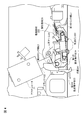
- FIG. 1 shows the overall configuration of the IC card processing device 1 in the present embodiment.
- the IC card processing apparatus 1 operates the IC contact unit 20 provided therein to read and write variable data such as transaction data recorded in the IC card.
- the IC card processing apparatus 1 is configured to include the transport roller 10 and the IC contact unit 20.
- the pair of transport rollers 10 are disposed vertically opposite to the card transport line X, and rotate so as to transport the IC card along the card transport line X.
- the transport roller 10 rotates so as to transport the IC card from right to left.
- the IC contact unit 20 is disposed between two sets of transport rollers 10 disposed in front of and behind the card transport line X, and is disposed above the card transport line X.
- the IC contact unit 20 reads and writes variable data recorded on the IC card transported along the card transport line X.
- the IC contact unit 20 presses the terminal (contact pin) on the IC contact unit 20 side into contact with the terminal on the IC card side by utilizing the transport force of the IC card.
- the detailed configuration of the IC contact unit 20 will be described below with reference to FIGS. 2 to 6.
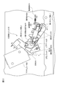
- FIG. 2 shows the overall configuration of the IC contact unit 20 in standby of the IC card.
- the IC contact unit 20 includes an actuator 21, a plunger 22, an L-shaped arm 23, a first contact terminal block 24, a second contact terminal block 25, an elastic member 26, a tension member 31, and the like.
- the actuator 21 When the IC card is transported along the card transport line X, the actuator 21 sucks the plunger 22 at a predetermined timing.
- the predetermined timing is, for example, a timing at which a claw portion 241 described later can lock the end portion of the IC card.
- the plunger 22 is connected to the L-arm 23 while being connected to the actuator 21 so as to be capable of suctioning.
- the plunger 22 transmits a suction operation to the L-shaped arm 23 when it is sucked by the actuator 21.
- one end of the L-shaped arm 23 which is a connection portion with the plunger 22 moves in the suction direction of the plunger 22.
- the L-shaped arm 23 rotates clockwise about a fixed axis for fixing the L-shaped arm 23, and the other end presses the first contact terminal block 24.
- the first link portion L1, the second link portion L2, and the rotational operation limiting portion move in the card transport line X direction. On the other hand, it is rotatably fixed while maintaining a predetermined angle ⁇ 1. On the other hand, when the first contact terminal block 24 is pressed by the L-shaped arm 23, it rotates counterclockwise with the first link portion L1 as a rotation axis.
- An installation area of the second contact terminal block 25 is formed at the central portion of the first contact terminal block 24, and a claw portion 241 is formed at the end.
- the claws 241 move downward below the card transport line X.
- the first contact terminal block 24 transmits the rotation operation to the second contact terminal block 25 via the second link portion L2 when the claw portion 241 moves downward.
- the second contact terminal block 25 is provided with a contact pin 251 at the central portion for actually reading and writing variable data recorded in the IC card, and an end portion of the second contact terminal block 25 is connected via the second link portion L2. It is connected to the first contact terminal block 24. At the other end, a stretching member 252 is formed, and the elastic member 26 is stretched on the stretching member 252.
- the second contact terminal block 25 is in a state in which the elastic member 26 is stretched on the stretching member 252 when the rotational operation from the first contact terminal block 24 is transmitted through the second link portion L2. As it is, it rotates counterclockwise with the first contact terminal block 24.
- the elastic member 26 is installed so that a biasing force acts in a direction substantially parallel to the card transfer line X direction and in a direction opposite to the transfer direction of the IC card at the time of IC card standby, and is an end of the second contact terminal block 25 It is stretched between the stretching member 252 and another stretching member 31.
- the elastic member 26 biases the second contact terminal block 25 to the right via the stretching member 252.
- the elastic member 26 is, for example, a spring coil.
- FIG. 3 shows the entire configuration of the IC contact unit 20 at the time of IC card locking.
- the first contact terminal block 24 In a state in which the claws 241 move below the card transfer line X, the first contact terminal block 24 maintains a substantially horizontal state with respect to the card transfer line X. That is, when the IC card is locked, the first contact terminal block 24 maintains the angle ⁇ 1 with respect to the card transport line X direction at 0. In this state, when the IC card is transported along the card transport line X, the first contact terminal block 24 locks the end of the IC card by the claw portion 241.
- the second contact terminal block 25 also rotates in the same direction as the first contact terminal block 24 rotates counterclockwise. However, the second contact terminal block 25 is a first contact terminal. Unlike the base 24, the base member 24 is rotated in the rightward direction by the elastic member 26 via the stretching member 252. Right and upward forces are applied to the second contact terminal block 25 after rotation.
- the second contact terminal block 25 when the IC card is locked is fixed in a state in which the predetermined angle ⁇ 2 is maintained with respect to the card transport line X direction. Therefore, it is possible to set a state in which the distance (retraction amount) between the contact pin 251 and the card transport line X at the time of IC card locking is separated by a fixed distance.
- FIG. 4 shows the overall configuration of the IC contact unit 20 during IC card transfer.
- the IC contact unit 20 locks the IC card by the claws 241
- the IC contact unit 20 receives the IC card conveyance force.
- the first contact terminal block 24 moves in the left direction. Further, this movement operation is transmitted to the second contact terminal block 25 via the second link portion L2.
- the second contact terminal block 25 moves leftward while the elastic member 26 is stretched by the stretching member 252.
- the guide shaft 253 formed on the second contact terminal block 25 abuts on the guide groove 32 and then the second contact terminal block 25 further moves in the left direction, the guide shaft 253 follows the guide groove 32. Guide in the lower left direction.
- the second contact terminal block 25 resists the upward force biased by the elastic member 26, and the tension member 252 side The end of the is pushed down. As a result, the contact pin 251 is pressed by the IC card and makes contact. At this time, the contact pin 251 contacts the IC card for the first time.
- FIG. 5 shows the overall configuration of the IC contact unit 20 when reading an IC card.
- the first contact terminal block 24 of the IC contact unit 20 moves leftward to a predetermined position. Further, with the movement of the first contact terminal block 24, the second contact terminal block 25 is also moved leftward to a predetermined position with the contact pins 251 pressed against the IC card.
- the IC contact unit 20 is formed with a guide groove (not shown) for restricting the movement of the first contact terminal block 24 in the left direction (not shown). Stops after moving leftward to a predetermined position. Since the second contact terminal block 25 is connected to the first contact terminal block 24 by the second link portion L2, the second contact terminal block 25 is stopped when the first contact terminal block 24 is stopped.
- FIG. 6 is an exploded perspective view of the IC contact unit 20. As shown in FIG. Here, the illustrated members will be described in order from the left.
- the elastic member 26 is, for example, a spring such as a spring coil, and one end is connected to the stretching member 252 and the other end is connected to the stretching member 31.
- the elastic member 26 always biases the tension member 252 toward the tension member 31 with respect to the second contact terminal block 25.
- the second contact terminal block 25 includes a contact pin 251 in addition to the stretching member 252 connected to the elastic member 26, and a second link portion L2 is formed.
- the contact pin 251 does not contact the IC card at the time of standby and contact of the IC card (FIGS. 1 to 3), and contacts the IC card only at the time of IC card transport (FIG. 4). Further, after moving to a predetermined position, the variable data of the IC card is read and written (FIG. 5).
- the second link portion L2 is rotatably connected to the convex portion formed on the first contact terminal block 24.
- the first contact terminal block 24 has a convex portion connected to the second link portion L2 and a first link portion L1.
- the first link portion L1 is movably connected to a guide groove 33 formed in the bracket 30.
- the moving direction is the card transport line X direction.
- the L-shaped arm 23 is connected to the plunger 22 and the rotary shaft 34 formed on the bracket 30, so that the L-arm 23 rotates around the rotary shaft 34 as the plunger 22 sucks.
- the plunger 22 is attracted, the L-shaped arm 23 rotates clockwise to press the first contact terminal block 24.
- the pressed first contact terminal block 24 locks the IC card conveyed by the claws 241.
- the bracket 30 is formed with the guide groove 32 in addition to the stretching member 31 and the guide groove 33 described above.
- the guide groove 32 restricts the operation of the second contact terminal block 25 when the first contact terminal block 24 moves in the card transport line X direction with the IC card. Specifically, while moving in the card transfer line X direction, the end on the side of the stretching member 252 is pushed downward to move the contact pin 251 so as to press the IC card.
- the actuator 21 moves the claw portion 241 downward to the card transport line X. It may be a compact one having a driving force, and the miniaturization of the entire apparatus and the reduction of power consumption can be achieved.
- the contact at the time of waiting and locking of the IC card The amount of retraction of the pin 251 can be increased. Therefore, destruction of the contact pin 251 can be avoided while achieving downsizing and power saving of the entire device.
Landscapes
- Physics & Mathematics (AREA)
- General Physics & Mathematics (AREA)
- Engineering & Computer Science (AREA)
- Theoretical Computer Science (AREA)
- Credit Cards Or The Like (AREA)
- Conveying Record Carriers (AREA)
- Coupling Device And Connection With Printed Circuit (AREA)
Abstract
Description
図1は、本実施の形態におけるICカード処理装置1の全体構成を示す。ICカード処理装置1は、ICカードが挿入されると、内部に備えるIC接点ユニット20を動作させ、ICカードに記録されている取引データ等の可変データを読み書きするように構成される。
図2は、ICカード待機時におけるIC接点ユニット20の全体構成を示す。IC接点ユニット20は、アクチュエータ21、プランジャ22、L字アーム23、第1の接点端子台24、第2の接点端子台25、弾性部材26及び張架部材31等を備えて構成される。
図3は、ICカード係止時におけるIC接点ユニット20の全体構成を示す。IC接点ユニット20は、ICカードがカード搬送ラインXに沿って搬送されてくると、所定のタイミングでプランジャ22を吸引する。プランジャ22の吸引動作に伴い、L字アーム23が時計回りに回転して第1の接点端子台24の爪部241側の端部を押下する。その結果、爪部241がカード搬送ラインXの下方に移動する。
図4は、ICカード搬送時におけるIC接点ユニット20の全体構成を示す。IC接点ユニット20は、爪部241によりICカードを係止すると、ICカードの搬送力を受ける。その結果、第1の接点端子台24が左方向に移動する。またこの移動動作を第2のリンク部L2を介して第2の接点端子台25に伝達する。
図5は、ICカード読み取り時におけるIC接点ユニット20の全体構成を示す。IC接点ユニット20の第1の接点端子台24は、ICカードの搬送力を受けると、所定の位置まで左方向に移動する。また第1の接点端子台24の移動に伴い、第2の接点端子台25も接点ピン251をICカードに押圧して接触させた状態のまま、所定の位置まで左方向に移動する。
図6は、IC接点ユニット20の分解斜視図である。ここでは図示されている部材を左から順に説明する。
以上のように本実施の形態におけるICカード処理装置1及びIC接点ユニット20によれば、アクチュエータ21は爪部241をカード搬送ラインXの下方に移動させる程度の駆動力をもった小型のものでよく、装置全体の小型化及び消費電力の低減を図ることができる。また接点ピン251を備える第2の接点端子台25の一端を第1の接点端子台24に接続し、他端を弾性部材26により引っ張るようにしたので、ICカード待機時及び係止時における接点ピン251の退避量を大きくすることができる。よって装置全体の小型化及び省電力化を図りつつ、接点ピン251が破壊されることを回避することができる。
20 IC接点ユニット
21 アクチュエータ
22 プランジャ
23 L字アーム
24 第1の接点端子台
241 爪部
25 第2の接点端子台
251 接点ピン
252 張架部材
253 案内軸
26 弾性部材
30 ブラケット
31 張架部材
32 ガイド溝
L1 第1のリンク部
L2 第2のリンク部
Claims (9)
- ICカードに対してデータを読み書きするIC接点ユニットにおいて、
第1の接点端子台と、第2の接点端子台と、弾性部材とを備え、
前記第1の接点端子台は、
前記ICカードを係止する爪部と、
前記第1の接点端子台が回転動作する際に回転軸となる第1のリンク部とを備え、
前記第2の接点端子台は、
前記ICカードの端子に接触する接点ピンと、
前記第1の接点端子台に回転可能に接続される第2のリンク部と、
前記弾性部材が張架される張架部材とを備え、
前記弾性部材は、
前記張架部材を介して前記第2の接点端子台に引っ張り力を付勢する
ことを特徴とするIC接点ユニット。 - 前記第1の接点端子台は、
中央部に前記第2の接点端子台を設置する設置領域が形成されており、
両端部のうちの一方に前記爪部が形成されており、
他端部に前記第1のリンク部が形成されており、
前記ICカードが搬送ラインに沿って搬送されてくると、前記第1のリンク部を回転軸として回転動作し、回転動作に伴って、前記爪部が前記搬送ラインよりも上方の位置から前記搬送ラインよりも下方の位置に移動する
ことを特徴とする請求項1に記載のIC接点ユニット。 - 前記第2の接点端子台は、
中央部に前記接点ピンが設置されており、
両端部のうちの一方に前記第2のリンク部が形成されており、
他端部に前記張架部材が形成されており、
前記ICカードが搬送ラインに沿って搬送されてくると、前記第1の接点端子台の回転動作に伴って、前記張架部材に前記弾性部材が張架された状態のまま、前記第2のリンク部が前記爪部とともに移動する
ことを特徴とする請求項2に記載のIC接点ユニット。 - 前記弾性部材は、
前記第1の接点端子台が回転動作した後のICカード係止時において、前記接点ピンが前記搬送ラインよりも一定の距離だけ上方に位置するように、前記第2の接点端子台に対して前記引っ張り力を付勢する
ことを特徴とする請求項3に記載のIC接点ユニット。 - 前記第1の接点端子台は、
前記搬送ラインに沿って搬送されてきたICカードの端部を前記爪部により係止すると、前記ICカードの搬送力を受けて、所定の距離だけ搬送方向に移動する
ことを特徴とする請求項4に記載のIC接点ユニット。 - 前記第2の接点端子台は、
前記第1の接点端子台が所定の距離だけ搬送方向に移動することに伴って、前記張架部材に前記弾性部材が張架された状態のまま、所定の距離だけ搬送方向に移動する
ことを特徴とする請求項5に記載のIC接点ユニット。 - 前記第2の接点端子台は、
案内軸が形成されており、
前記所定の距離だけ搬送方向に移動する際、前記案内軸がガイド溝に沿って案内されることにより、前記弾性部材により付勢されている前記引っ張り力に抗って、前記接点ピンを前記ICカードの端子に押圧する
ことを特徴とする請求項6に記載のIC接点ユニット。 - 請求項1ないし請求項7の何れか一項に記載の前記IC接点ユニットを備えた
ことを特徴とするICカード処理装置。 - 請求項8に記載の前記ICカード処理装置を備えた
ことを特徴とする自動取引装置。
Priority Applications (3)
| Application Number | Priority Date | Filing Date | Title |
|---|---|---|---|
| CN201480016708.4A CN105453111B (zh) | 2014-06-11 | 2014-06-11 | Ic触点单元以及ic卡处理装置 |
| JP2016527537A JP6167234B2 (ja) | 2014-06-11 | 2014-06-11 | Ic接点ユニット及びicカード処理装置 |
| PCT/JP2014/065412 WO2015189923A1 (ja) | 2014-06-11 | 2014-06-11 | Ic接点ユニット及びicカード処理装置 |
Applications Claiming Priority (1)
| Application Number | Priority Date | Filing Date | Title |
|---|---|---|---|
| PCT/JP2014/065412 WO2015189923A1 (ja) | 2014-06-11 | 2014-06-11 | Ic接点ユニット及びicカード処理装置 |
Publications (1)
| Publication Number | Publication Date |
|---|---|
| WO2015189923A1 true WO2015189923A1 (ja) | 2015-12-17 |
Family
ID=54833054
Family Applications (1)
| Application Number | Title | Priority Date | Filing Date |
|---|---|---|---|
| PCT/JP2014/065412 Ceased WO2015189923A1 (ja) | 2014-06-11 | 2014-06-11 | Ic接点ユニット及びicカード処理装置 |
Country Status (3)
| Country | Link |
|---|---|
| JP (1) | JP6167234B2 (ja) |
| CN (1) | CN105453111B (ja) |
| WO (1) | WO2015189923A1 (ja) |
Families Citing this family (2)
| Publication number | Priority date | Publication date | Assignee | Title |
|---|---|---|---|---|
| JP6324617B2 (ja) | 2015-04-10 | 2018-05-16 | 日立オムロンターミナルソリューションズ株式会社 | Ic接点ユニット、icカード処理装置及び自動取引装置 |
| JP6737677B2 (ja) * | 2016-09-30 | 2020-08-12 | 日本電産サンキョー株式会社 | カード発行装置 |
Citations (5)
| Publication number | Priority date | Publication date | Assignee | Title |
|---|---|---|---|---|
| DE3916783A1 (de) * | 1988-10-19 | 1990-04-26 | Landis & Gyr Ag | Vorrichtung zum lesen und/oder beschreiben von chip-karten |
| JPH0714014A (ja) * | 1993-06-23 | 1995-01-17 | Sankyo Seiki Mfg Co Ltd | 接点の上下装置 |
| JPH0997313A (ja) * | 1995-10-02 | 1997-04-08 | Nippon Conlux Co Ltd | 情報記録再生装置 |
| JPH10106678A (ja) * | 1996-09-25 | 1998-04-24 | Sankyo Seiki Mfg Co Ltd | Ic接点の圧着機構 |
| WO2010052755A1 (ja) * | 2008-11-07 | 2010-05-14 | 日立オムロンターミナルソリューションズ株式会社 | カードリーダ |
Family Cites Families (2)
| Publication number | Priority date | Publication date | Assignee | Title |
|---|---|---|---|---|
| JP3022842B2 (ja) * | 1998-06-26 | 2000-03-21 | 株式会社タツノ・メカトロニクス | Icカード読取り・書き込み装置 |
| CN101599582B (zh) * | 2004-03-18 | 2011-11-09 | 山一电机株式会社 | Ic卡用连接器 |
-
2014
- 2014-06-11 WO PCT/JP2014/065412 patent/WO2015189923A1/ja not_active Ceased
- 2014-06-11 JP JP2016527537A patent/JP6167234B2/ja active Active
- 2014-06-11 CN CN201480016708.4A patent/CN105453111B/zh active Active
Patent Citations (5)
| Publication number | Priority date | Publication date | Assignee | Title |
|---|---|---|---|---|
| DE3916783A1 (de) * | 1988-10-19 | 1990-04-26 | Landis & Gyr Ag | Vorrichtung zum lesen und/oder beschreiben von chip-karten |
| JPH0714014A (ja) * | 1993-06-23 | 1995-01-17 | Sankyo Seiki Mfg Co Ltd | 接点の上下装置 |
| JPH0997313A (ja) * | 1995-10-02 | 1997-04-08 | Nippon Conlux Co Ltd | 情報記録再生装置 |
| JPH10106678A (ja) * | 1996-09-25 | 1998-04-24 | Sankyo Seiki Mfg Co Ltd | Ic接点の圧着機構 |
| WO2010052755A1 (ja) * | 2008-11-07 | 2010-05-14 | 日立オムロンターミナルソリューションズ株式会社 | カードリーダ |
Also Published As
| Publication number | Publication date |
|---|---|
| JPWO2015189923A1 (ja) | 2017-04-20 |
| CN105453111A (zh) | 2016-03-30 |
| CN105453111B (zh) | 2018-03-02 |
| JP6167234B2 (ja) | 2017-07-19 |
Similar Documents
| Publication | Publication Date | Title |
|---|---|---|
| WO2017005093A1 (zh) | 分纸机构及使用该分纸机构的薄片类介质处理装置 | |
| WO2015189923A1 (ja) | Ic接点ユニット及びicカード処理装置 | |
| JP6552603B2 (ja) | Icカードリーダ | |
| JP6324617B2 (ja) | Ic接点ユニット、icカード処理装置及び自動取引装置 | |
| JP5833420B2 (ja) | 媒体処理装置 | |
| CN105320972B (zh) | 卡处理装置及自动交易装置 | |
| US9583850B1 (en) | Connector module with a reseat actuator | |
| JP2003108937A (ja) | Icカードリーダ | |
| JP2750070B2 (ja) | 接点の上下装置 | |
| KR101858979B1 (ko) | 카드 처리 장치 및 자동 거래 장치 | |
| KR101320777B1 (ko) | 매체자동지급기의 카드 독취장치 및 그 방법 | |
| KR101034970B1 (ko) | 매체자동지급기의 매체분기장치 | |
| JP3864917B2 (ja) | カード処理装置 | |
| CN107004143B (zh) | 卡处理装置 | |
| JP3369045B2 (ja) | Icカードリーダ | |
| JP2004280567A (ja) | カード処理装置 | |
| JP2009015627A (ja) | カードの挟み込み搬送装置 | |
| JP2005135159A (ja) | 接触型icカード処理装置 | |
| JPS63247248A (ja) | 用紙アライニング機構 | |
| JPH1021344A (ja) | カード処理装置 | |
| TW201520081A (zh) | 紙張傳輸裝置 | |
| TW201520065A (zh) | 紙張傳輸裝置 | |
| CN104649046A (zh) | 纸张传输装置 | |
| JPS5922182A (ja) | 通帳記帳機 | |
| JPS6055872B2 (ja) | 磁気カ−ド搬送装置 |
Legal Events
| Date | Code | Title | Description |
|---|---|---|---|
| WWE | Wipo information: entry into national phase |
Ref document number: 201480016708.4 Country of ref document: CN |
|
| 121 | Ep: the epo has been informed by wipo that ep was designated in this application |
Ref document number: 14894693 Country of ref document: EP Kind code of ref document: A1 |
|
| ENP | Entry into the national phase |
Ref document number: 2016527537 Country of ref document: JP Kind code of ref document: A |
|
| NENP | Non-entry into the national phase |
Ref country code: DE |
|
| 122 | Ep: pct application non-entry in european phase |
Ref document number: 14894693 Country of ref document: EP Kind code of ref document: A1 |