WO2015186504A1 - 発光デバイス、波長変換部材及び波長変換部材の製造方法 - Google Patents
発光デバイス、波長変換部材及び波長変換部材の製造方法 Download PDFInfo
- Publication number
- WO2015186504A1 WO2015186504A1 PCT/JP2015/064306 JP2015064306W WO2015186504A1 WO 2015186504 A1 WO2015186504 A1 WO 2015186504A1 JP 2015064306 W JP2015064306 W JP 2015064306W WO 2015186504 A1 WO2015186504 A1 WO 2015186504A1
- Authority
- WO
- WIPO (PCT)
- Prior art keywords
- porous body
- wavelength conversion
- conversion member
- quantum dots
- emitting device
- Prior art date
- Legal status (The legal status is an assumption and is not a legal conclusion. Google has not performed a legal analysis and makes no representation as to the accuracy of the status listed.)
- Ceased
Links
Images



Classifications
-
- C—CHEMISTRY; METALLURGY
- C04—CEMENTS; CONCRETE; ARTIFICIAL STONE; CERAMICS; REFRACTORIES
- C04B—LIME, MAGNESIA; SLAG; CEMENTS; COMPOSITIONS THEREOF, e.g. MORTARS, CONCRETE OR LIKE BUILDING MATERIALS; ARTIFICIAL STONE; CERAMICS; REFRACTORIES; TREATMENT OF NATURAL STONE
- C04B38/00—Porous mortars, concrete, artificial stone or ceramic ware; Preparation thereof
-
- C—CHEMISTRY; METALLURGY
- C04—CEMENTS; CONCRETE; ARTIFICIAL STONE; CERAMICS; REFRACTORIES
- C04B—LIME, MAGNESIA; SLAG; CEMENTS; COMPOSITIONS THEREOF, e.g. MORTARS, CONCRETE OR LIKE BUILDING MATERIALS; ARTIFICIAL STONE; CERAMICS; REFRACTORIES; TREATMENT OF NATURAL STONE
- C04B41/00—After-treatment of mortars, concrete, artificial stone or ceramics; Treatment of natural stone
- C04B41/80—After-treatment of mortars, concrete, artificial stone or ceramics; Treatment of natural stone of only ceramics
- C04B41/81—Coating or impregnation
- C04B41/85—Coating or impregnation with inorganic materials
-
- C—CHEMISTRY; METALLURGY
- C09—DYES; PAINTS; POLISHES; NATURAL RESINS; ADHESIVES; COMPOSITIONS NOT OTHERWISE PROVIDED FOR; APPLICATIONS OF MATERIALS NOT OTHERWISE PROVIDED FOR
- C09K—MATERIALS FOR MISCELLANEOUS APPLICATIONS, NOT PROVIDED FOR ELSEWHERE
- C09K11/00—Luminescent materials, e.g. electroluminescent or chemiluminescent
- C09K11/08—Luminescent materials, e.g. electroluminescent or chemiluminescent containing inorganic luminescent materials
-
- H—ELECTRICITY
- H10—SEMICONDUCTOR DEVICES; ELECTRIC SOLID-STATE DEVICES NOT OTHERWISE PROVIDED FOR
- H10H—INORGANIC LIGHT-EMITTING SEMICONDUCTOR DEVICES HAVING POTENTIAL BARRIERS
- H10H20/00—Individual inorganic light-emitting semiconductor devices having potential barriers, e.g. light-emitting diodes [LED]
- H10H20/80—Constructional details
- H10H20/85—Packages
- H10H20/851—Wavelength conversion means
Definitions
- the present invention relates to a light emitting device, a wavelength conversion member, and a method for manufacturing the wavelength conversion member.
- Patent Document 1 discloses a light-emitting device that includes a blue LED and a sealing portion that seals the blue LED, and the sealing portion is made of a resin composition containing quantum dots.
- the light emission intensity of the light emitting device described in Patent Document 1 depends on the thickness of the sealing portion.
- the sealing part is configured with a resin composition containing quantum dots
- the thickness of the sealing part varies due to the shrinkage of the resin when the sealing part is dried, and the thickness of the sealing part is made uniform. It is difficult. Therefore, the light emitting device described in Patent Document 1 has a problem that it is difficult to reduce the unevenness of the light emission intensity.
- the main object of the present invention is to provide a light emitting device having a configuration capable of reducing variations in characteristics such as light emission intensity.
- a light emitting device includes: a wavelength conversion member that emits light having a wavelength different from that of excitation light when excitation light is incident; and a light source that irradiates the wavelength conversion member with excitation light.
- the wavelength conversion member has a porous body and the quantum dot carry
- the porous body may be composed of a green compact or a sintered body of a plurality of particles.
- the quantum dots can be suitably supported on the inner surface of the porous body.
- the porous body may have open cells.
- the quantum dots can be preferably introduced into the porous body through the open cells, the quantum dots can be suitably supported on the inner surface of the porous body.
- the porous body is preferably made of an inorganic material.
- the porous body is hardly deteriorated by light from the light source or the quantum dots.
- the mechanical strength of the porous body can be increased.
- the porous body may be composed of at least one selected from the group consisting of glass, silica, alumina, zirconia and hafnia. In this case, it can suppress more effectively that a porous body deteriorates with the light from a light source or a quantum dot. Moreover, the mechanical strength of the porous body can be increased more effectively.
- the wavelength conversion member may further have a coating film covering at least a part of the outer surface of the porous body.
- the coating film can suppress contact between the quantum dots and oxygen or moisture, so that deterioration of the quantum dots due to oxygen or moisture can be suppressed.
- the coating film is composed of at least one selected from the group consisting of glass, silica, alumina, zinc oxide, ITO (indium tin oxide), magnesium fluoride, and cerium fluoride. Also good. In this case, since the permeability of oxygen and moisture in the coating film is low, deterioration due to oxygen and moisture in the quantum dots can be more effectively suppressed.
- the wavelength conversion member may further include a cell for sealing the porous body carrying the quantum dots.
- the contact between the quantum dots contained in the wavelength conversion member and oxygen and moisture can be more effectively suppressed by the cell, deterioration of the quantum dots due to oxygen and moisture can be further suppressed.
- the average pore diameter of the porous body may be 0.01 ⁇ m to 500 ⁇ m.
- the quantum dots can be suitably supported on the inner surface of the porous body.
- the porous body may have a portion having a thickness of 5 mm or less.
- the thickness of the porous body is as thin as 5 mm or less, it is possible to suppress excessive scattering of light inside the porous body. For this reason, it can suppress that the transmittance
- the wavelength conversion member according to the present invention includes a porous body and quantum dots carried on the inner surface of the porous body. In this case, since the variation in the thickness of the porous body carrying the quantum dots can be suppressed, the variation in the emission intensity and the like can be reduced.
- the first wavelength conversion member manufacturing method includes a step of preparing a porous body having open cells, a step of impregnating the porous body with a liquid containing quantum dots, and an impregnation with a liquid containing quantum dots A step of obtaining a wavelength conversion member having a porous body and quantum dots carried on the inner surface of the porous body by drying the porous body.
- the quantum dots can be suitably introduced into the porous body through the open cells, and variation in the thickness of the porous body carrying the quantum dots can be suppressed, so that the emission intensity of the wavelength conversion member, etc. Variation can be reduced.
- the liquid contains at least one selected from the group consisting of hexane, heptane, nonane, chloroform, toluene, octane, diethyl ether, ethyl acetate, and methylene chloride. May be. Since these liquids have a low boiling point, the liquid can be easily removed from the porous body.
- the manufacturing method of the first wavelength conversion member according to the present invention may further include a step of sealing the dried porous body with a cell.
- the first wavelength conversion member manufacturing method includes a step of disposing a porous body in a cell having a through hole, a liquid containing quantum dots from the through hole, and a liquid containing quantum dots.
- a step of impregnating the porous body and a step of closing the through hole after drying the porous body impregnated with the liquid containing quantum dots may be further provided.
- the second method for producing a wavelength conversion member according to the present invention includes a step of preparing a paste having carrier particles and quantum dots, a step of forming a paste to obtain a molded body, and drying the molded body. And a step of obtaining a wavelength conversion member having a porous body constituted by carrier particles and quantum dots carried on the inner surface of the porous body.
- a step of firing the molded body may be further performed.
- firing the molded body it is possible to suppress a change in the thickness of the porous body due to heat generated during light emission, and thus variations in characteristics such as light emission intensity of the light emitting device can be reduced.
- a light emitting device having a configuration capable of reducing variations in characteristics such as light emission intensity.
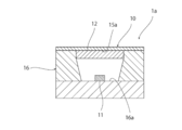
- FIG. 1 is a schematic cross-sectional view of the light emitting device according to the first embodiment.
- FIG. 2 is a schematic cross-sectional view of a part of the wavelength conversion member.
- FIG. 3 is a schematic cross-sectional view of the light emitting device according to the second embodiment.
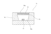
- FIG. 4 is a schematic cross-sectional view of the light emitting device according to the third embodiment.
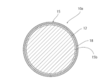
- FIG. 5 is a schematic perspective view of a wavelength conversion member according to the fourth embodiment.
- FIG. 6 is a schematic cross-sectional view of a wavelength conversion member according to the fourth embodiment.
- FIG. 7 is a schematic cross-sectional view of a light emitting device according to a fifth embodiment.
- FIG. 1 is a schematic cross-sectional view of a light emitting device 1 according to the first embodiment.
- the light emitting device 1 includes a wavelength conversion member 10 and a light source 11.
- the wavelength conversion member 10 is a member that emits light having a wavelength different from that of the excitation light when the excitation light is incident.
- the light source 11 emits excitation light to the wavelength conversion member 10.
- substantially all of the light emitted from the light source 11 may be absorbed by the wavelength conversion member 10, or part of the light may pass through the wavelength conversion member 10. That is, the light emitting device 1 may be a device that emits mixed light of light emitted from the light source 11 and transmitted through the wavelength conversion member 10 and light emitted from the wavelength conversion member 10.
- the light source 11 can be composed of, for example, an LED (Light Emitting Diode) element, an LD (Laser Diode) element, or the like.
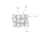
- FIG. 2 is a schematic cross-sectional view of a part of the wavelength conversion member 10.
- the wavelength conversion member 10 includes a porous body 12.
- the porous body 12 is composed of a green compact of a plurality of carrier particles 13.
- the particle diameter of the carrier particles 13 is preferably 0.5 ⁇ m to 10 ⁇ m, and more preferably 1 ⁇ m to 3 ⁇ m.
- the particle diameter of the carrier particles 13 is too small, the porosity of the porous body 12 is lowered, and it may be difficult to carry the quantum dots 14 on the inner surface of the porous body 12.
- the wavelength conversion member is produced by impregnating the porous body 12 with the liquid containing the quantum dots 14, the solvent is less likely to volatilize from the porous body 12.
- the particle diameter of the carrier particles 13 is too large, the porosity of the porous body 12 increases, light scattering becomes too large, and the transmittance tends to decrease.
- the porosity of the porous body 12 is not particularly limited, but is preferably about 5% to 45%, for example, and more preferably 5% to 40%. If the porosity of the porous body 12 is too low, it may be difficult to carry the quantum dots 14 on the inner surface of the porous body 12. In addition, when the wavelength conversion member is manufactured by impregnating the porous body 12 with the liquid containing the quantum dots 14, the solvent may not easily evaporate from the porous body 12. On the other hand, if the porosity of the porous body 12 becomes too large, light scattering may become too large and the transmittance may be easily lowered.
- the average pore diameter of the porous body 12 is not particularly limited, but is preferably 0.01 ⁇ m to 500 ⁇ m, and more preferably 20 ⁇ m to 100 ⁇ m. If the average pore diameter of the porous body 12 is too small, it may be difficult to carry the quantum dots 14 on the inner surface of the porous body 12. In addition, when the wavelength conversion member is manufactured by impregnating the porous body 12 with the liquid containing the quantum dots 14, the solvent may not easily evaporate from the porous body 12. On the other hand, if the average pore diameter of the porous body 12 is too large, light scattering may become too large and the transmittance may be likely to decrease. The average pore diameter of the porous body 12 can be measured by a multipoint BET method or the like.
- the porous body 12 preferably has a portion having a thickness (t) of 5 mm or less. If the thickness (t) of the porous body 12 is too large, light scattering may become too large, and the transmittance may be easily lowered. However, if the thickness (t) of the porous body 12 is too thin, it is difficult to alleviate the uneven light emission in the surface, and the variation in characteristics such as the light emission intensity of the light emitting device may increase. Therefore, the thickness (t) of the porous body 12 is preferably 0.1 mm or more.
- the carrier particles 13 are preferably made of an inorganic material.
- the carrier particles 13 are preferably composed of at least one selected from the group consisting of glass, silica, alumina, zirconia, and hafnia, for example. In this case, it can suppress more effectively that a porous body deteriorates with the light from a light source or a quantum dot. Moreover, the mechanical durability of the porous body can be increased more effectively.
- the carrier particles 13 are preferably spherical. In this case, excessive scattering of light on the inner surface of the porous body 12 can be suppressed. Therefore, the light emitting device 1 having high light extraction efficiency can be obtained.
- the porous body 12 when the porous body 12 is made of an inorganic material, the porous body 12 is unlikely to be deteriorated by light from the light source 11 or light emitted from the quantum dots 14. Further, the mechanical durability of the porous body 12 can be increased.
- quantum dots 14 are carried on the inner surface of the porous body 12.
- the wavelength conversion member 10 may include one type of quantum dot 14 or may include a plurality of types of quantum dots 14. By including a plurality of types of quantum dots 14, it is possible to give a range to the color tone of the converted light.
- the quantum dots 14 emit light having a wavelength different from that of the excitation light when the excitation light of the quantum dot 14 is incident.
- the wavelength of light emitted from the quantum dot 14 depends on the particle diameter of the quantum dot 14. That is, the wavelength of the light obtained by changing the particle diameter of the quantum dots 14 can be adjusted. For this reason, the particle diameter of the quantum dot 14 is set to a particle diameter corresponding to the wavelength of light to be obtained.
- the particle diameter of the quantum dots 14 is usually about 2 nm to 10 nm.
- the particle diameter is 2.0 nm to 3.0 nm.
- quantum dot 14 that emits green visible light (fluorescence having a wavelength of 500 nm to 540 nm) when irradiated with ultraviolet to near ultraviolet excitation light having a wavelength of 300 nm to 440 nm or blue excitation light having a wavelength of 440 nm to 480 nm include particles Examples thereof include CdSe / ZnS microcrystals having a diameter of about 3.0 nm to 3.3 nm.
- quantum dots 14 that emit yellow visible light (fluorescence having a wavelength of 540 nm to 595 nm) when irradiated with ultraviolet to near ultraviolet excitation light having a wavelength of 300 nm to 440 nm or blue excitation light having a wavelength of 440 nm to 480 nm include particles Examples thereof include CdSe / ZnS microcrystals having a diameter of about 3.3 nm to 4.5 nm.
- quantum dots 14 that emit red visible light (fluorescence having a wavelength of 600 nm to 700 nm) when irradiated with ultraviolet to near ultraviolet excitation light having a wavelength of 300 nm to 440 nm or blue excitation light having a wavelength of 440 nm to 480 nm include particles Examples thereof include CdSe / ZnS microcrystals having a diameter of about 4.5 nm to 10 nm.
- the ratio of the particle diameter of the carrier particles 13 to the particle diameter of the quantum dots 14 is preferably 10 or more, and 100 or more. Is more preferable.
- the ratio of the particle diameter of the carrier particles 13 to the particle diameter of the quantum dots 14 is preferably 100,000 or less, and preferably 10,000 or less. Is more preferable. If the ratio of the particle diameter of the carrier particles 13 to the particle diameter of the quantum dots 14 ((particle diameter of the carrier particles 13) / (particle diameter of the quantum dots 14)) is too small, the porosity of the porous body 12 is decreased.
- the quantum dots 14 are less likely to be supported on the inner surface of the porous body 12.
- the solvent may not easily evaporate from the porous body 12.
- the ratio of the particle diameter of the carrier particles 13 to the particle diameter of the quantum dots 14 ((particle diameter of the carrier particles 13) / (particle diameter of the quantum dots 14)) is too large, the porosity of the porous body 12 is increased. In some cases, the light scattering becomes too large and the transmittance tends to decrease.
- the wavelength conversion member 10 includes a cell 15 that seals the porous body 12. For this reason, the contact of the quantum dot 14 contained in the wavelength conversion member 10, oxygen, and a water
- the cell 15 is preferably made of an inorganic material, and more preferably made of a glass material, a ceramic material, or the like. In this case, the contact of the quantum dots 14 contained in the wavelength conversion member 10 with oxygen and moisture can be suppressed more reliably.
- a wavelength conversion member formed of a resin composition in which quantum dots are dispersed can be formed by, for example, printing and drying a paste containing quantum dots and a resin. it can.
- the concentration of resin or the like in the paste may change, or the temperature of the paste may change.
- coating of a paste may change.
- the thickness tends to change.
- the wavelength conversion member changes, the amount of excitation light absorbed by the wavelength conversion member and the amount of light emitted from the wavelength conversion member change. Therefore, when the wavelength conversion member is composed of a resin composition in which quantum dots are dispersed, the emission intensity unevenness tends to increase.
- quantum dots 14 are carried on the inner surface of the porous body 12.
- the volume shrinkage rate at the time of manufacturing can be reduced, so it is relatively easy to reduce the manufacturing unevenness of the thickness of the porous body 12. Therefore, according to the wavelength conversion member 10, variations in characteristics such as light emission intensity can be reduced.
- the manufacturing method of the wavelength conversion member 10 is not specifically limited.
- the wavelength conversion member 10 can be manufactured, for example, in the following manner.
- the porous body 12 is produced.
- the porous body 12 can be formed, for example, by firing a molded body obtained by molding a paste containing the carrier particles 13.
- the molded body may contain, for example, a disappearing agent such as resin or carbon, an inorganic binder, or the like.
- the porous body 12 is impregnated in the liquid containing the quantum dots 14.
- the liquid containing the quantum dots 14 is caused to enter the porous body 12 by immersing the porous body 12 in the liquid containing the quantum dots 14.
- the porous body 12 preferably has open cells.
- the quantum dots 14 can be carried on the inner surface of the porous body 12.
- the liquid containing the quantum dots 14 may contain, for example, at least one selected from the group consisting of hexane, heptane, nonane, chloroform, toluene, octane, diethyl ether, ethyl acetate, and methylene chloride. These liquids have a low boiling point. For this reason, the liquid can be easily removed from the porous body 12 by using these liquids.
- the porous body 12 may be sealed with the cells 15.
- the wavelength conversion member 10 can be manufactured through the above steps.
- the quantum dots 14 are carried. For this reason, it is not necessary to expose the quantum dot 14 to the high heat at the time of baking. Therefore, deterioration due to heat at the time of manufacturing the wavelength conversion member 10 can be suppressed, and the quantum dots 14 having low heat resistance can also be used. Moreover, if it is the porous body 12, compared with the resin composition which disperse
- a paste having carrier particles 13 and quantum dots 14 is prepared.
- the paste is molded to obtain a molded body.
- the method for forming the paste is not particularly limited.
- the paste may be formed by printing by a printing method such as a screen printing method or an ink jet printing method and then drying. Further, for example, a paste printed on a thick film may be further press-molded.
- the wavelength conversion member 10 can be obtained by drying the molded body. In addition, you may obtain the wavelength conversion member 10 by baking after drying a molded object. In that case, the wavelength conversion member 10 comprised by the sintered body can be manufactured. If the wavelength conversion member 10 is composed of a fired body, the thickness of the wavelength conversion member 10 can be prevented from changing due to heat generated during light emission. Variation can be reduced.
- FIG. 2 is commonly referred to in the second and third embodiments.
- FIG. 3 is a schematic cross-sectional view of a light emitting device 1a according to the second embodiment.
- the present invention is not limited to this configuration.
- the wavelength conversion member 10 is provided on a part of one surface so that the wavelength conversion member 10 is sealed in the recess of the device body 16 having the light source 11 on the mounting substrate 16a.
- the cover member 15a made of the formed transparent inorganic material (for example, glass material, ceramic material, etc.) and the device body 16 may be integrated.
- the wavelength conversion member 10 is sealed in the device body 16 by the cover member 15a, contact between the quantum dots 14 included in the wavelength conversion member 10 and oxygen and moisture can be suppressed.
- the arrangement accuracy of the light source 11 and the wavelength conversion member 10 can be increased.
- the light emitting device 1a can be further downsized.
- FIG. 4 is a schematic cross-sectional view of a light emitting device 1b according to the third embodiment.
- the coating film 17 As shown in FIG. 4, in the light emitting device 1 b, at least a part of the outer surface of the porous body 12 is covered with the coating film 17. For this reason, contact between the quantum dots 14 contained in the porous body 12 and oxygen or moisture can be suppressed. Accordingly, it is possible to suppress the deterioration of the quantum dots 14 due to oxygen and moisture. From the viewpoint of more effectively suppressing deterioration of the quantum dots 14 due to oxygen and moisture, at least a portion of the outer surface of the porous body 12 that is not covered by the cover member 15a is covered. Is more preferable, and it is more preferable to cover the entire outer surface of the porous body 12.
- the coating film 17 is preferably made of an inorganic material, and is made of glass, silica, alumina, zinc oxide, indium tin oxide. More preferably, it is composed of at least one selected from the group consisting of an object (ITO), magnesium fluoride and cerium fluoride.
- the thickness of the coating film 17 is preferably 0.01 ⁇ m to 20 ⁇ m, and more preferably 1 ⁇ m to 5 ⁇ m. If the thickness of the coating film 17 is too small, it may be difficult to obtain the effect of suppressing the intrusion of oxygen and moisture. On the other hand, if the thickness of the coating film 17 is too large, cracks are likely to occur in the coating film, and it may be difficult to obtain the effect of suppressing the entry of oxygen and moisture.
- FIG. 5 is a schematic perspective view of a wavelength conversion member 10a according to the fourth embodiment.
- FIG. 6 is a schematic cross-sectional view of a wavelength conversion member 10a according to the fourth embodiment.
- the present invention is not limited to this.
- the produced porous body 12 is arranged in the cell 15 having the through hole 15b.
- the porous body 12 is manufactured by applying a paste for forming the porous body 12 on the substrate, drying the paste, and then baking the paste. Thereafter, in the periphery of the porous body 12, the porous body 12 is disposed inside by fusing the substrate and another substrate disposed on the substrate using an inorganic fusing agent such as glass.
- a cell 15 can be produced.
- the porous body 12 impregnated with the liquid containing the quantum dots 14 is dried.
- the porous body 12 can be dried by reducing the pressure while heating the cell 15. From the viewpoint of suitably drying the porous body 12, it is preferable to provide a plurality of through holes 15b.
- the liquid containing the quantum dot 14 can be suitably inject
- the through hole 15b of the cell 15 is closed.
- the through hole 15b can be closed by fusing an inorganic sealing material such as glass.
- the wavelength conversion member 10a can be obtained by the above process.
- the liquid containing the quantum dots 14 is impregnated and dried. Therefore, it can suppress more effectively that the quantum dot 14 contacts oxygen and moisture. Accordingly, it is possible to suppress the deterioration of the quantum dots 14 due to oxygen and moisture.
- a reflection member 18 is provided on the inner surface of the cell 15. For this reason, it is possible to prevent light from being emitted from the inner wall of the cell 15.
- FIG. 7 is a schematic cross-sectional view of a light emitting device 1c according to the fifth embodiment. As illustrated in FIG. 7, the wavelength conversion member 10 a according to the fourth embodiment may be attached to the device body 16 on which the light source 11 is mounted.
Landscapes
- Chemical & Material Sciences (AREA)
- Engineering & Computer Science (AREA)
- Ceramic Engineering (AREA)
- Materials Engineering (AREA)
- Organic Chemistry (AREA)
- Inorganic Chemistry (AREA)
- Structural Engineering (AREA)
- Led Device Packages (AREA)
- Luminescent Compositions (AREA)
Abstract
発光強度等の特性の製造ばらつきを小さくし得る構成を有する発光デバイスを提供する。 発光デバイス1は、波長変換部材10と、光源11とを備える。波長変換部材10は、励起光が入射したときに、励起光とは波長が異なる波長の光を出射する。光源11は、波長変換部材10に励起光を照射する。波長変換部材10は、多孔質体12と、量子ドット14とを有する。量子ドット14は、多孔質体12の内表面上に担持されている。
Description
本発明は、発光デバイス、波長変換部材及び波長変換部材の製造方法に関する。
近年、発光ダイオードを用いた発光デバイスの進歩が目覚しく、液晶のバックライト、大型ディスプレイ等に採用されている。特に、短波長光の発光素子の半導体材料の発展により、短波長の光を得られるようになってきたため、これを用いて蛍光体を励起してより多様な波長の光を得ることができるようになった。
従来より、量子ドットを用いた発光デバイスが知られている。例えば、特許文献1には、青色LEDと、青色LEDを封止する封止部を備え、封止部が量子ドットを含む樹脂組成物からなる発光デバイスが開示されている。
特許文献1に記載の発光デバイスの発光強度は、封止部の厚みに左右される。しかしながら、量子ドットを含む樹脂組成物により封止部を構成した場合、封止部を乾燥する際の樹脂の収縮により、封止部の厚みにばらつきが生じ、封止部の厚みを均一にすることは困難である。従って、特許文献1に記載の発光デバイスには、発光強度のむらを小さくすることが困難であるという問題がある。 本発明の主な目的は、発光強度等の特性のばらつきを小さくし得る構成を有する発光デバイスを提供することにある。
本発明に係る発光デバイスは、励起光が入射したときに、励起光とは波長が異なる波長の光を出射する波長変換部材と、波長変換部材に励起光を照射する光源と、を備える発光デバイスであって、波長変換部材は、多孔質体と、多孔質体の内表面上に担持された量子ドットと、を有する。この場合、量子ドットを担持した多孔質体の厚みのばらつきを抑制できるため、発光強度等のばらつきを小さくし得る。
本発明に係る発光デバイスでは、多孔質体が、複数の粒子の圧粉体又は焼結体により構成されていてもよい。多孔質体を圧粉体又は焼結体とすることで、量子ドットを多孔質体の内表面上に好適に担持できる。
本発明に係る発光デバイスでは、多孔質体が、連続気泡を有していてもよい。この場合、連続気泡を通じて多孔質体の内部に量子ドットを好適に導入できるため、量子ドットを多孔質体の内表面上に好適に担持させることができる。
本発明に係る発光デバイスでは、多孔質体が、無機材により構成されていることが好ましい。この場合、多孔質体が光源や量子ドットからの光によって劣化し難くなる。また、多孔質体の機械的強度を高めることができる。
本発明に係る発光デバイスでは、多孔質体が、ガラス、シリカ、アルミナ、ジルコニア及びハフニアからなる群から選ばれた少なくとも一種により構成されていてもよい。この場合、多孔質体が光源や量子ドットからの光によって劣化することをより効果的に抑制できる。また、多孔質体の機械的強度をより効果的に高めることができる。
本発明に係る発光デバイスは、波長変換部材が、多孔質体の外表面の少なくとも一部を覆うコーティング膜をさらに有していてもよい。この場合、コーティング膜により、量子ドットと、酸素や水分との接触を抑制できるので、量子ドットの酸素や水分に起因する劣化を抑制することができる。
本発明に係る発光デバイスでは、コーティング膜が、ガラス、シリカ、アルミナ、酸化亜鉛、ITO(インジウムスズ酸化物)、フッ化マグネシウム及びフッ化セリウムからなる群から選ばれた少なくとも一種により構成されていてもよい。この場合、コーティング膜の酸素や水分の透過度が低いため、量子ドットの酸素や水分に起因する劣化をより効果的に抑制することができる。
本発明に係る発光デバイスでは、波長変換部材は、量子ドットが担持された多孔質体を封止するセルをさらに有していてもよい。この場合、セルによって、波長変換部材中に含まれる量子ドットと、酸素及び水分との接触をより効果的に抑制できるので、量子ドットの酸素や水分に起因する劣化をさらに抑制することができる。
本発明に係る発光デバイスでは、多孔質体の平均細孔径が、0.01μm~500μmであってもよい。この場合、量子ドットを多孔質体の内表面上に好適に担持させることができる。
本発明に係る発光デバイスでは、多孔質体は、厚みが5mm以下の部分を有していてもよい。この場合、多孔質体の厚みが5mm以下と薄いので、多孔質体の内部で光が過剰に散乱することを抑制できる。このため、光の透過率が低くなりすぎることを抑制することができる。
本発明に係る波長変換部材は、多孔質体と、多孔質体の内表面上に担持された量子ドットと、を備える。この場合、量子ドットを担持した多孔質体の厚みのばらつきを抑制できるため、発光強度等のばらつきを小さくし得る。
本発明に係る第1の波長変換部材の製造方法は、連続気泡を有する多孔質体を準備する工程と、量子ドットを含む液体を多孔質体に含浸させる工程と、量子ドットを含む液体を含浸した多孔質体を乾燥させることにより、多孔質体と、多孔質体の内表面上に担持された量子ドットとを有する波長変換部材を得る工程と、を備える。このようにすることにより、連続気泡を通じて多孔質体の内部に量子ドットを好適に導入できると共に、量子ドットを担持した多孔質体の厚みのばらつきを抑制できるため、波長変換部材の発光強度等のばらつきを小さくできる。
本発明に係る第1の波長変換部材の製造方法では、液体は、ヘキサン、ヘプタン、ノナン、クロロホルム、トルエン、オクタン、ジエチルエーテル、酢酸エチル及び塩化メチレンからなる群から選ばれた少なくとも一種を含んでいてもよい。これらの液体は、低い沸点を有するため、多孔質体から液体を容易に除去することができる。
本発明に係る第1の波長変換部材の製造方法は、乾燥させた多孔質体をセルで封止する工程をさらに含んでいてもよい。このようにすることにより、量子ドットと、酸素及び水分との接触を抑制することができる。よって、量子ドットの酸素や水分に起因する劣化を抑制することができる。
本発明に係る第1の波長変換部材の製造方法は、多孔質体を、貫通孔を有するセル内に配する工程と、貫通孔から量子ドットを含む液体を注入し、量子ドットを含む液体を多孔質体に含浸させる工程と、量子ドットを含む液体を含浸した多孔質体を乾燥させた後に、貫通孔を塞ぐ工程と、をさらに備えていてもよい。このようにすることにより、量子ドットと、酸素及び水分との接触をより効果的に抑制することができる。よって、量子ドットの酸素や水分に起因する劣化をより効果的に抑制することができる。
本発明に係る第2の波長変換部材の製造方法は、担体粒子と、量子ドットとを有するペーストを調製する工程と、ペーストを成形し、成形体を得る工程と、成形体を乾燥させることにより、担体粒子により構成された多孔質体と、多孔質体の内表面上に担持された量子ドットとを有する波長変換部材を得る工程と、を備える。このようにすることにより、量子ドットを担持した多孔質体の厚みのばらつきを抑制できるため、発光デバイスの発光強度等の特性のばらつきを小さくできる。
本発明に係る第2の波長変換部材の製造方法では、成形体を焼成する工程をさらに行ってもよい。成形体を焼成することにより、発光の際に発生する熱によって、多孔質体の厚みが変化することを抑制することができるため、発光デバイスの発光強度等の特性のばらつきを小さくできる。
本発明によれば、発光強度等の特性のばらつきを小さくし得る構成を有する発光デバイスを提供することができる。
以下、本発明を実施した好ましい形態について説明する。但し、下記の実施形態は、単なる例示である。本発明は、下記の実施形態に何ら限定されない。
また、実施形態等において参照する各図面において、実質的に同一の機能を有する部材は同一の符号で参照することとする。また、実施形態等において参照する図面は、模式的に記載されたものである。図面に描画された物体の寸法の比率などは、現実の物体の寸法の比率などとは異なる場合がある。図面相互間においても、物体の寸法比率等が異なる場合がある。具体的な物体の寸法比率等は、以下の説明を参酌して判断されるべきである。
(第1の実施形態)
図1は、第1の実施形態に係る発光デバイス1の模式的断面図である。
図1は、第1の実施形態に係る発光デバイス1の模式的断面図である。
図1に示すように、発光デバイス1は、波長変換部材10と、光源11とを備える。
波長変換部材10は、励起光が入射したときに、励起光とは波長が異なる波長の光を出射する部材である。光源11は、波長変換部材10に対して励起光を出射する。発光デバイス1においては、光源11から出射された光の実質的にすべてが波長変換部材10により吸収されてもよいし、一部の光が波長変換部材10を透過してもよい。すなわち、発光デバイス1は、光源11から出射され波長変換部材10を透過した光と、波長変換部材10から出射した光との混合光を出射するデバイスであってもよい。
光源11は、例えば、LED(Light Emitting Diode)素子、LD(Laser Diode)素子等により構成することができる。
図2は、波長変換部材10の一部分の模式的断面図である。図2に示すように、波長変換部材10は、多孔質体12を備える。本実施形態では、多孔質体12は、複数の担体粒子13の圧粉体により構成されている。担体粒子13の粒子径は、0.5μm~10μmであることが好ましく、1μm~3μmであることがより好ましい。なお、担体粒子13の粒子径が小さすぎると、多孔質体12の気孔率が低下し、量子ドット14を多孔質体12の内表面上に担持させにくくなる場合がある。また、量子ドット14を含む液体に多孔質体12を含浸させて波長変換部材を作製する際に、多孔質体12から、溶媒が揮発しにくくなる。一方、担体粒子13の粒子径が大きすぎると、多孔質体12の気孔率が増大し、光の散乱が大きくなりすぎて透過率が低下しやすくなる場合がある。
多孔質体12の気孔率は、特に限定されないが、例えば、5%~45%程度であることが好ましく、5%~40%であることがより好ましい。なお、多孔質体12の気孔率が低くなりすぎると、量子ドット14を多孔質体12の内表面上に担持させにくくなる場合がある。また、量子ドット14を含む液体に多孔質体12を含浸させて波長変換部材を作製する際に、多孔質体12から、溶媒が揮発しにくくなる場合がある。一方、多孔質体12の気孔率が大きくなりすぎると、光の散乱が大きくなりすぎて透過率が低下しやすくなる場合がある。
多孔質体12の平均細孔径は、特に限定されないが、0.01μm~500μmであることが好ましく、20μm~100μmであることがより好ましい。多孔質体12の平均細孔径が小さすぎると、量子ドット14を多孔質体12の内表面上に担持させにくくなる場合がある。また、量子ドット14を含む液体に多孔質体12を含浸させて波長変換部材を作製する際に、多孔質体12から、溶媒が揮発しにくくなる場合がある。一方、多孔質体12の平均細孔径が大きすぎると、光の散乱が大きくなりすぎて透過率が低下しやすくなる場合がある。多孔質体12の平均細孔径は、多点BET法等により測定することができる。
多孔質体12は、厚み(t)が5mm以下の部分を有することが好ましい。多孔質体12の厚み(t)が大きすぎると、光の散乱が大きくなりすぎて透過率が低下しやすくなる場合がある。但し、多孔質体12の厚み(t)が薄すぎると、面内における発光むらを緩和しにくくなり、発光デバイスの発光強度等の特性のばらつきが大きくなる場合がある。従って、多孔質体12の厚み(t)は、0.1mm以上であることが好ましい。
担体粒子13は、無機材により構成されていることが好ましい。具体的には、担体粒子13は、例えば、ガラス、シリカ、アルミナ、ジルコニア及びハフニアからなる群から選ばれた少なくとも一種により構成されていることが好ましい。この場合、多孔質体が光源や量子ドットからの光によって劣化することをより効果的に抑制できる。また、多孔質体の機械的耐久性をより効果的に高めることができる。
担体粒子13は、球状であることが好ましい。この場合、多孔質体12の内表面において光が過剰に散乱することを抑制することができる。従って、光の取り出し効率が高い発光デバイス1を得ることができる。
本実施形態のように、多孔質体12を無機材により構成することにより、光源11からの光や量子ドット14から出射された光により多孔質体12が劣化し難い。また、多孔質体12の機械的耐久性を高めることができる。
波長変換部材10では、多孔質体12の内表面に量子ドット14が担持されている。波長変換部材10は、1種類の量子ドット14を含んでいてもよいし、複数種類の量子ドット14を含んでいてもよい。複数種類の量子ドット14を含有させることで、変換光の色調に幅を持たせることが可能となる。
なお、量子ドット14は、量子ドット14の励起光が入射したときに、励起光とは異なる波長の光を出射する。量子ドット14から出射される光の波長は、量子ドット14の粒子径に依存する。すなわち、量子ドット14の粒子径を変化させることにより得られる光の波長を調整することができる。このため、量子ドット14の粒子径は、得ようとする光の波長に応じた粒子径とされている。量子ドット14の粒子径は、通常、2nm~10nm程度である。
例えば、波長300nm~440nmの紫外~近紫外の励起光を照射すると青色の可視光(波長440nm~480nmの蛍光)を発する量子ドット14の具体例としては、粒子径が2.0nm~3.0nm程度のCdSe/ZnSの微結晶などが挙げられる。波長300nm~440nmの紫外~近紫外の励起光や波長440nm~480nmの青色の励起光を照射すると緑色の可視光(波長が500nm~540nmの蛍光)を発する量子ドット14の具体例としては、粒子径が3.0nm~3.3nm程度のCdSe/ZnSの微結晶などが挙げられる。波長300nm~440nmの紫外~近紫外の励起光や波長440nm~480nmの青色の励起光を照射すると黄色の可視光(波長が540nm~595nmの蛍光)を発する量子ドット14の具体例としては、粒子径が3.3nm~4.5nm程度のCdSe/ZnSの微結晶などが挙げられる。波長300nm~440nmの紫外~近紫外の励起光や波長440nm~480nmの青色の励起光を照射すると赤色の可視光(波長が600nm~700nmの蛍光)を発する量子ドット14の具体例としては、粒子径が4.5nm~10nm程度のCdSe/ZnSの微結晶などが挙げられる。
量子ドット14の粒子径に対する、担体粒子13の粒子径の比((担体粒子13の粒子径)/(量子ドット14の粒子径))は、10以上であることが好ましく、100以上であることがより好ましい。量子ドット14の粒子径に対する、担体粒子13の粒子径の比((担体粒子13の粒子径)/(量子ドット14の粒子径))は、100000以下であることが好ましく、10000以下であることがより好ましい。なお、量子ドット14の粒子径に対する、担体粒子13の粒子径の比((担体粒子13の粒子径)/(量子ドット14の粒子径))が小さすぎると、多孔質体12の気孔率が低下し、量子ドット14を多孔質体12の内表面上に担持させにくくなる場合がある。また、量子ドット14を含む液体に多孔質体12を含浸させて波長変換部材を作製する際に、多孔質体12から、溶媒が揮発しにくくなる場合がある。一方、量子ドット14の粒子径に対する、担体粒子13の粒子径の比((担体粒子13の粒子径)/(量子ドット14の粒子径))が大きすぎると、多孔質体12の気孔率が増大し、光の散乱が大きくなりすぎて透過率が低下しやすくなる場合がある。
図1に示すように、波長変換部材10は、多孔質体12を封止するセル15を備えている。このため、波長変換部材10中に含まれる量子ドット14と、酸素及び水分との接触を抑制することができる。従って、量子ドット14の酸素や水分に起因する劣化を抑制することができる。また、セル15と光源11とが離間しているため、光源11の熱によりセル15内の量子ドット14が劣化し難い。
量子ドット14の劣化をより効果的に抑制する観点から、セル15は、無機材により構成されていることが好ましく、ガラス材、セラミック材等により構成されていることがより好ましい。この場合、より確実に、波長変換部材10中に含まれる量子ドット14と、酸素及び水分との接触を抑制することができる。
例えば特許文献1に記載のように、量子ドットを分散させた樹脂組成物により構成された波長変換部材は、例えば、量子ドットと樹脂とを含むペーストを印刷し、乾燥させることにより形成することができる。このような方法で形成した波長変換部材においては、例えば、ペーストにおける樹脂等の濃度が変化したり、ペーストの温度が変化したりすることがある。このため、ペーストの塗布時における粘度が変化する場合がある。ペーストの粘度が変化すると、厚みが変化しやすい。波長変換部材の厚みが変化すると、波長変換部材により吸収される励起光の量や、波長変換部材からの出射光の量が変化する。従って、量子ドットを分散させた樹脂組成物により波長変換部材が構成されている場合は、発光強度むらが大きくなりやすい。
それに対して波長変換部材10では、多孔質体12の内表面に量子ドット14が担持されている。ペーストの塗膜の厚みの製造むらを小さくすることに比べ、製造時の体積収縮率を低くできるため、多孔質体12の厚みの製造むらを小さくすることは比較的容易である。従って、波長変換部材10によれば、発光強度等の特性のばらつきを小さくし得る。
〔波長変換部材10の製造方法〕
波長変換部材10の製造方法は、特に限定されない。波長変換部材10は、例えば、以下の要領で製造することができる。
波長変換部材10の製造方法は、特に限定されない。波長変換部材10は、例えば、以下の要領で製造することができる。
〈第1の製造方法〉
まず、多孔質体12を作製する。多孔質体12は、例えば、担体粒子13を含むペーストを成形して得られた成形体を焼成することにより形成することができる。成形体には、例えば、樹脂やカーボン等の消失剤や、無機結合剤等を含ませておいてもよい。
まず、多孔質体12を作製する。多孔質体12は、例えば、担体粒子13を含むペーストを成形して得られた成形体を焼成することにより形成することができる。成形体には、例えば、樹脂やカーボン等の消失剤や、無機結合剤等を含ませておいてもよい。
次に、量子ドット14を含む液体に多孔質体12を含浸させる。具体的には、量子ドット14を含む液体に多孔質体12を浸漬することにより、多孔質体12内に、量子ドット14を含む液体を侵入させる。多孔質体12に液体を好適に含浸させる観点からは、多孔質体12が連続気泡を有することが好ましい。
次に、量子ドット14を含む液体を含浸した多孔質体12を乾燥させることにより、多孔質体12の気泡内に位置している液体を除去する。これにより、多孔質体12の内表面に量子ドット14を担持させることができる。
量子ドット14を含む液体は、例えば、ヘキサン、ヘプタン、ノナン、クロロホルム、トルエン、オクタン、ジエチルエーテル、酢酸エチル及び塩化メチレンからなる群から選ばれた少なくとも一種を含んでいてもよい。これらの液体は、低い沸点を有する。このため、これらの液体を用いることにより、多孔質体12から液体を容易に除去することができる。
多孔質体12を乾燥させた後に、多孔質体12をセル15で封止してもよい。
以上の工程により、波長変換部材10を製造することができる。
第1の製造方法では、多孔質体12を作製した後に、量子ドット14を担持させる。このため、量子ドット14を焼成時の高熱に曝す必要がない。従って、波長変換部材10を製造する際の熱による劣化を抑制できるとともに、耐熱性の低い量子ドット14をも使用し得る。また、多孔質体12であれば、量子ドットを分散させた樹脂組成物に比べて、製造時における体積収縮率が低く、多孔質体12の厚みの製造ばらつきを抑えることができる。よって、発光強度等の特性のばらつきを小さくし得る。
〈第2の製造方法〉
第2の製造方法では、まず、担体粒子13と量子ドット14とを有するペーストを調製する。次に、そのペーストを成形し、成形体を得る。ペーストの成形方法は、特に限定されない。例えば、ペーストを、スクリーン印刷法やインクジェット印刷法等の印刷法により印刷し、乾燥させることにより成形してもよい。また、例えば、厚膜に印刷したペーストをさらにプレス成形してもよい。
第2の製造方法では、まず、担体粒子13と量子ドット14とを有するペーストを調製する。次に、そのペーストを成形し、成形体を得る。ペーストの成形方法は、特に限定されない。例えば、ペーストを、スクリーン印刷法やインクジェット印刷法等の印刷法により印刷し、乾燥させることにより成形してもよい。また、例えば、厚膜に印刷したペーストをさらにプレス成形してもよい。
次に、成形体を乾燥させることにより、波長変換部材10を得ることができる。なお、成形体を乾燥させた後に、焼成することにより波長変換部材10を得てもよい。その場合は、焼成体により構成された波長変換部材10を製造することができる。焼成体により構成された波長変換部材10であれば、発光の際に発生する熱によって、波長変換部材10の厚みが変化することを抑制することができるため、発光デバイスの発光強度等の特性のばらつきを小さくできる。
以下、本発明の好ましい実施形態の他の例について説明する。以下の説明において、上記第1の実施形態と実質的に共通の機能を有する部材を共通の符号で参照し、説明を省略する。図2は、第2及び第3の実施形態において共通に参照する。
(第2の実施形態)
図3は、第2の実施形態に係る発光デバイス1aの模式的断面図である。
図3は、第2の実施形態に係る発光デバイス1aの模式的断面図である。
第1の実施形態では、光源11がセル15の外部に配されている例について説明した。但し、本発明は、この構成に限定されない。図3に示すように、実装基板16aの上に光源11を備えたデバイス本体16の凹部内に、波長変換部材10が封止されるように、一方の表面の一部に波長変換部材10を形成した透明な無機材(例えば、ガラス材、セラミック材等)からなるカバー部材15aとデバイス本体16とを一体化してもよい。この場合、波長変換部材10は、カバー部材15aでデバイス本体16内に封止されるため、波長変換部材10中に含まれる量子ドット14と、酸素及び水分との接触を抑制することができる。また、光源11と波長変換部材10との配置精度を高くすることができる。さらに、発光デバイス1aをより小型化し得る。
(第3の実施形態)
図4は、第3の実施形態に係る発光デバイス1bの模式的断面図である。
図4は、第3の実施形態に係る発光デバイス1bの模式的断面図である。
図4に示すように、発光デバイス1bでは、多孔質体12の外表面の少なくとも一部がコーティング膜17により覆われている。このため、多孔質体12に含まれる量子ドット14と、酸素や水分との接触を抑制することができる。従って、量子ドット14の酸素や水分に起因する劣化を抑制することができる。量子ドット14の酸素や水分に起因する劣化をより効果的に抑制する観点からは、多孔質体12の外表面のうち、少なくともカバー部材15aにより覆われていない部分の実質的に全体を覆うことがより好ましく、多孔質体12の外表面の全体を覆うことがさらに好ましい。
多孔質体12内への酸素や水分の侵入をより効果的に抑制する観点からは、コーティング膜17が無機材により構成されていることが好ましく、ガラス、シリカ、アルミナ、酸化亜鉛、インジウムスズ酸化物(ITO)、フッ化マグネシウム及びフッ化セリウムからなる群から選ばれた少なくとも一種により構成されていることがより好ましい。コーティング膜17の厚みは、0.01μm~20μmであることが好ましく、1μm~5μmであることがより好ましい。なお、コーティング膜17の厚みが小さすぎると、酸素や水分の侵入を抑制する効果が得にくくなる場合がある。一方、コーティング膜17の厚みが大きすぎると、コーティング膜にクラックが発生しやすくなり、酸素や水分の侵入を抑制する効果が得にくくなる場合がある。
(第4の実施形態)
図5は、第4の実施形態に係る波長変換部材10aの模式的斜視図である。図6は、第4の実施形態に係る波長変換部材10aの模式的断面図である。
図5は、第4の実施形態に係る波長変換部材10aの模式的斜視図である。図6は、第4の実施形態に係る波長変換部材10aの模式的断面図である。
第1の実施形態における第1の製造方法では、量子ドット14を含む液体に含浸させた多孔質体12を乾燥させた後に、セル15により多孔質体12を封止する例について説明したが、本発明はこれに限定されない。
第4の実施形態では、図6に示すように、多孔質体12をセル15内に配した後に、量子ドット14を含む液体を多孔質体12に含浸させる例について説明する。
第4の実施形態では、まず、作製した多孔質体12を、貫通孔15bを有するセル15内に配する。例えば、基板の上に、多孔質体12を構成するためのペーストを塗布し、乾燥させた後に焼成することにより多孔質体12を作製する。その後、多孔質体12の周辺部において、基板と、基板の上に配された別の基板とをガラスなどの無機融着剤を用いて融着することにより、内部に多孔質体12が配されたセル15を作製することができる。
次に、貫通孔15bから、量子ドット14を含む液体を注入する。これにより、量子ドット14を含む液体を多孔質体12に含浸させる。
次に、量子ドット14を含む液体を含浸した多孔質体12を乾燥させる。具体的には、例えば、セル15を加熱しながら減圧することにより、多孔質体12を乾燥させることができる。多孔質体12を好適に乾燥させる観点からは、貫通孔15bを複数設けておくことが好ましい。また、貫通孔15bを複数設けておくことにより、量子ドット14を含む液体を好適に注入することができる。
次に、セル15の貫通孔15bを塞ぐ。具体的には、例えば、ガラス等の無機封止材を融着させることにより貫通孔15bを塞ぐことができる。
上記工程により、波長変換部材10aを得ることができる。
第4の実施形態では、多孔質体12をセル15内に配した後に、量子ドット14を含む液体に含浸させ、乾燥させる。よって、量子ドット14が酸素や水分と接触することをより効果的に抑制することができる。従って、量子ドット14の酸素や水分に起因する劣化を抑制することができる。
波長変換部材10aでは、セル15の内側面の上に、反射部材18が設けられている。このため、セル15の内壁から光が出射することを抑制することができる。
(第5の実施形態)
図7は、第5の実施形態に係る発光デバイス1cの模式的断面図である。図7に示すように、第4の実施形態に係る波長変換部材10aを、光源11が搭載されたデバイス本体16に取り付けてもよい。
図7は、第5の実施形態に係る発光デバイス1cの模式的断面図である。図7に示すように、第4の実施形態に係る波長変換部材10aを、光源11が搭載されたデバイス本体16に取り付けてもよい。
1,1a,1b,1c 発光デバイス
10,10a 波長変換部材
11 光源
12 多孔質体
13 担体粒子
14 量子ドット
15 セル
15a カバー部材
15b 貫通孔
16 デバイス本体
16a 実装基板
17 コーティング膜
18 反射部材
10,10a 波長変換部材
11 光源
12 多孔質体
13 担体粒子
14 量子ドット
15 セル
15a カバー部材
15b 貫通孔
16 デバイス本体
16a 実装基板
17 コーティング膜
18 反射部材
Claims (17)
- 励起光が入射したときに、前記励起光とは波長が異なる波長の光を出射する波長変換部材と、
前記波長変換部材に前記励起光を照射する光源と、
を備える発光デバイスであって、
前記波長変換部材は、
多孔質体と、
前記多孔質体の内表面上に担持された量子ドットと、
を有する、発光デバイス。 - 前記多孔質体は、複数の粒子の圧粉体又は焼結体により構成されている、請求項1に記載の発光デバイス。
- 前記多孔質体は、連続気泡を有する、請求項1又は2に記載の発光デバイス。
- 前記多孔質体は、無機材により構成されている、請求項1~3のいずれか一項に記載の発光デバイス。
- 前記多孔質体は、ガラス、シリカ、アルミナ、ジルコニア及びハフニアからなる群から選ばれた少なくとも一種により構成されている、請求項1~4のいずれか一項に記載の発光デバイス。
- 前記波長変換部材は、前記多孔質体の外表面の少なくとも一部を覆うコーティング膜をさらに有する、請求項1~5のいずれか一項に記載の発光デバイス。
- 前記コーティング膜は、ガラス、シリカ、アルミナ、酸化亜鉛、ITO、フッ化マグネシウム及びフッ化セリウムからなる群から選ばれた少なくとも一種により構成されている、請求項6に記載の発光デバイス。
- 前記波長変換部材は、前記量子ドットが担持された多孔質体を封止するセルをさらに有する、請求項1~7のいずれか一項に記載の発光デバイス。
- 前記多孔質体の平均細孔径が、0.01μm~500μmである、請求項1~8のいずれか一項に記載の発光デバイス。
- 前記多孔質体は、厚みが5mm以下の部分を有する、請求項1~9のいずれか一項に記載の発光デバイス。
- 多孔質体と、
前記多孔質体の内表面上に担持された量子ドットと、
を備える、波長変換部材。 - 連続気泡を有する多孔質体を準備する工程と、
量子ドットを含む液体を前記多孔質体に含浸させる工程と、
前記量子ドットを含む液体を含浸した多孔質体を乾燥させることにより、前記多孔質体と、前記多孔質体の内表面上に担持された前記量子ドットとを有する波長変換部材を得る工程と、
を備える、波長変換部材の製造方法。 - 前記液体は、ヘキサン、ヘプタン、ノナン、クロロホルム、トルエン、オクタン、ジエチルエーテル、酢酸エチル及び塩化メチレンからなる群から選ばれた少なくとも一種を含む、請求項12に記載の波長変換部材の製造方法。
- 前記乾燥させた多孔質体をセルで封止する工程をさらに含む、請求項12又は13に記載の波長変換部材の製造方法。
- 前記多孔質体を、貫通孔を有するセル内に配する工程と、
前記貫通孔から前記量子ドットを含む液体を注入し、前記量子ドットを含む液体を多孔質体に含浸させる工程と、
前記量子ドットを含む液体を含浸した多孔質体を乾燥させた後に、前記貫通孔を塞ぐ工程と、
をさらに備える、請求項12又は13に記載の波長変換部材の製造方法。 - 担体粒子と、量子ドットとを有するペーストを調製する工程と、
前記ペーストを成形し、成形体を得る工程と、
前記成形体を乾燥させることにより、前記担体粒子により構成された多孔質体と、前記多孔質体の内表面上に担持された前記量子ドットとを有する波長変換部材を得る工程と、
を備える、波長変換部材の製造方法。 - 前記成形体を焼成する工程をさらに備える、請求項16に記載の波長変換部材の製造方法。
Applications Claiming Priority (4)
| Application Number | Priority Date | Filing Date | Title |
|---|---|---|---|
| JP2014-117997 | 2014-06-06 | ||
| JP2014117997 | 2014-06-06 | ||
| JP2014149456A JP6264218B2 (ja) | 2014-06-06 | 2014-07-23 | 発光デバイス、波長変換部材及び波長変換部材の製造方法 |
| JP2014-149456 | 2014-07-23 |
Publications (1)
| Publication Number | Publication Date |
|---|---|
| WO2015186504A1 true WO2015186504A1 (ja) | 2015-12-10 |
Family
ID=54766580
Family Applications (1)
| Application Number | Title | Priority Date | Filing Date |
|---|---|---|---|
| PCT/JP2015/064306 Ceased WO2015186504A1 (ja) | 2014-06-06 | 2015-05-19 | 発光デバイス、波長変換部材及び波長変換部材の製造方法 |
Country Status (3)
| Country | Link |
|---|---|
| JP (1) | JP6264218B2 (ja) |
| TW (1) | TW201547067A (ja) |
| WO (1) | WO2015186504A1 (ja) |
Cited By (4)
| Publication number | Priority date | Publication date | Assignee | Title |
|---|---|---|---|---|
| CN109424860A (zh) * | 2017-08-31 | 2019-03-05 | 日亚化学工业株式会社 | 荧光部件、光学零件及发光装置 |
| CN111273484A (zh) * | 2020-03-11 | 2020-06-12 | 宁波东旭成新材料科技有限公司 | 一种无阻隔膜量子点膜 |
| CN114512588A (zh) * | 2022-02-25 | 2022-05-17 | 苏州芯聚半导体有限公司 | 微发光二极管结构及制备方法、显示面板 |
| WO2022251195A1 (en) * | 2021-05-24 | 2022-12-01 | W. L. Gore & Associates, Inc. | Photoluminescent composites and processes for fabricating the same |
Families Citing this family (5)
| Publication number | Priority date | Publication date | Assignee | Title |
|---|---|---|---|---|
| TWI579635B (zh) * | 2015-12-28 | 2017-04-21 | 中強光電股份有限公司 | 投影系統及其屏幕 |
| WO2018030586A1 (ko) * | 2016-08-09 | 2018-02-15 | 주식회사 베이스 | 엘이디 색변환용 구조체 및 이를 포함하는 엘이디 패키지 |
| US11655415B2 (en) | 2017-06-19 | 2023-05-23 | Nippon Electric Glass Co., Ltd. | Nanophosphor-attached inorganic particles and wavelength conversion member |
| JP7124827B2 (ja) * | 2017-07-21 | 2022-08-24 | Dic株式会社 | インク組成物及びその製造方法、光変換層並びにカラーフィルタ |
| TWI650398B (zh) * | 2017-12-08 | 2019-02-11 | Chi Mei Corporation | 發光材料與應用之顯示裝置 |
Citations (4)
| Publication number | Priority date | Publication date | Assignee | Title |
|---|---|---|---|---|
| JPH05345685A (ja) * | 1992-06-15 | 1993-12-27 | Toshiba Ceramics Co Ltd | シリカ質多孔体の製造方法 |
| JP2003201473A (ja) * | 2001-10-31 | 2003-07-18 | Nittetsu Mining Co Ltd | 酸化亜鉛−シリカ系無機多孔質蛍光体及びその製造方法 |
| JP2012054585A (ja) * | 2003-04-10 | 2012-03-15 | Patent-Treuhand-Gesellschaft Fuer Elektrische Gluehlampen Mbh | 蛍光体を基礎とするled及びこれに属する蛍光体 |
| WO2012102107A1 (ja) * | 2011-01-28 | 2012-08-02 | 昭和電工株式会社 | 量子ドット蛍光体を含む組成物、量子ドット蛍光体分散樹脂成形体、量子ドット蛍光体を含む構造物、発光装置、電子機器、機械装置及び量子ドット蛍光体分散樹脂成形体の製造方法 |
-
2014
- 2014-07-23 JP JP2014149456A patent/JP6264218B2/ja not_active Expired - Fee Related
-
2015
- 2015-05-19 WO PCT/JP2015/064306 patent/WO2015186504A1/ja not_active Ceased
- 2015-06-01 TW TW104117673A patent/TW201547067A/zh unknown
Patent Citations (4)
| Publication number | Priority date | Publication date | Assignee | Title |
|---|---|---|---|---|
| JPH05345685A (ja) * | 1992-06-15 | 1993-12-27 | Toshiba Ceramics Co Ltd | シリカ質多孔体の製造方法 |
| JP2003201473A (ja) * | 2001-10-31 | 2003-07-18 | Nittetsu Mining Co Ltd | 酸化亜鉛−シリカ系無機多孔質蛍光体及びその製造方法 |
| JP2012054585A (ja) * | 2003-04-10 | 2012-03-15 | Patent-Treuhand-Gesellschaft Fuer Elektrische Gluehlampen Mbh | 蛍光体を基礎とするled及びこれに属する蛍光体 |
| WO2012102107A1 (ja) * | 2011-01-28 | 2012-08-02 | 昭和電工株式会社 | 量子ドット蛍光体を含む組成物、量子ドット蛍光体分散樹脂成形体、量子ドット蛍光体を含む構造物、発光装置、電子機器、機械装置及び量子ドット蛍光体分散樹脂成形体の製造方法 |
Cited By (7)
| Publication number | Priority date | Publication date | Assignee | Title |
|---|---|---|---|---|
| CN109424860A (zh) * | 2017-08-31 | 2019-03-05 | 日亚化学工业株式会社 | 荧光部件、光学零件及发光装置 |
| CN109424860B (zh) * | 2017-08-31 | 2023-05-02 | 日亚化学工业株式会社 | 荧光部件、光学零件及发光装置 |
| CN111273484A (zh) * | 2020-03-11 | 2020-06-12 | 宁波东旭成新材料科技有限公司 | 一种无阻隔膜量子点膜 |
| CN111273484B (zh) * | 2020-03-11 | 2023-08-22 | 宁波东旭成新材料科技有限公司 | 一种无阻隔膜量子点膜 |
| WO2022251195A1 (en) * | 2021-05-24 | 2022-12-01 | W. L. Gore & Associates, Inc. | Photoluminescent composites and processes for fabricating the same |
| CN114512588A (zh) * | 2022-02-25 | 2022-05-17 | 苏州芯聚半导体有限公司 | 微发光二极管结构及制备方法、显示面板 |
| CN114512588B (zh) * | 2022-02-25 | 2023-06-16 | 苏州芯聚半导体有限公司 | 微发光二极管结构及制备方法、显示面板 |
Also Published As
| Publication number | Publication date |
|---|---|
| TW201547067A (zh) | 2015-12-16 |
| JP2016012711A (ja) | 2016-01-21 |
| JP6264218B2 (ja) | 2018-01-24 |
Similar Documents
| Publication | Publication Date | Title |
|---|---|---|
| JP6264218B2 (ja) | 発光デバイス、波長変換部材及び波長変換部材の製造方法 | |
| JP4814540B2 (ja) | 蛍光体の製造方法 | |
| JP5749792B2 (ja) | 量子ドット・ガラス複合発光材料及びその製造方法 | |
| KR101642120B1 (ko) | 유기발광소자용 광추출 기판 제조방법, 유기발광소자용 광추출 기판 및 이를 포함하는 유기발광소자 | |
| CN104344328A (zh) | 一种用于高色域液晶显示器的背光模组及其制造方法 | |
| US20180138359A1 (en) | Stratified Quantum Dot Phosphor Structure | |
| TW201447464A (zh) | 一種波長轉換裝置及其製作方法 | |
| KR101318374B1 (ko) | 유기 전계 발광소자 및 그 제조 방법 | |
| CN101897040A (zh) | 具有混合顶部反射器的侧发射器件 | |
| JP5724684B2 (ja) | 発光デバイス用セル及び発光デバイス | |
| CN105158972A (zh) | 导光板及导光板的制备方法 | |
| CN106653985A (zh) | 一种多层封装的量子点led结构 | |
| CN104993037B (zh) | 一种发光二极管及其封装结构、封装方法和显示装置 | |
| US20160300985A1 (en) | Optoelectronic Device and Method for Producing an Optoelectronic Device | |
| TW201642458A (zh) | 有機發光顯示裝置及其製造方法 | |
| WO2015174127A1 (ja) | 発光デバイス及びその製造方法 | |
| CN116209927A (zh) | 一种滤光材料、显示模组及其制作方法 | |
| JP2014096334A (ja) | 有機エレクトロルミネッセンス素子 | |
| JP2005072129A (ja) | 可視光線発光装置とその製造方法及び表示装置 | |
| JP2018077324A (ja) | 波長変換部材及び発光装置 | |
| JP6134176B2 (ja) | 発光装置、および、その製造方法 | |
| KR101484089B1 (ko) | 초박형 유기발광소자 제조방법 | |
| JP2016081040A (ja) | 光反射材料、ならびに光反射材料を用いた発光装置 | |
| CN111081853A (zh) | Led组件、量子点led发光件、量子点led封装结构及显示设备 | |
| TWI538263B (zh) | 承載結構及發光裝置 |
Legal Events
| Date | Code | Title | Description |
|---|---|---|---|
| 121 | Ep: the epo has been informed by wipo that ep was designated in this application |
Ref document number: 15803737 Country of ref document: EP Kind code of ref document: A1 |
|
| NENP | Non-entry into the national phase |
Ref country code: DE |
|
| 122 | Ep: pct application non-entry in european phase |
Ref document number: 15803737 Country of ref document: EP Kind code of ref document: A1 |