WO2015182415A1 - 電子部品の気密封止用クラッド材及びその製造方法 - Google Patents
電子部品の気密封止用クラッド材及びその製造方法 Download PDFInfo
- Publication number
- WO2015182415A1 WO2015182415A1 PCT/JP2015/064145 JP2015064145W WO2015182415A1 WO 2015182415 A1 WO2015182415 A1 WO 2015182415A1 JP 2015064145 W JP2015064145 W JP 2015064145W WO 2015182415 A1 WO2015182415 A1 WO 2015182415A1
- Authority
- WO
- WIPO (PCT)
- Prior art keywords
- kovar
- layer
- crystal grains
- clad material
- clad
- Prior art date
- Legal status (The legal status is an assumption and is not a legal conclusion. Google has not performed a legal analysis and makes no representation as to the accuracy of the status listed.)
- Ceased
Links
Classifications
-
- H—ELECTRICITY
- H10—SEMICONDUCTOR DEVICES; ELECTRIC SOLID-STATE DEVICES NOT OTHERWISE PROVIDED FOR
- H10W—GENERIC PACKAGES, INTERCONNECTIONS, CONNECTORS OR OTHER CONSTRUCTIONAL DETAILS OF DEVICES COVERED BY CLASS H10
- H10W76/00—Containers; Fillings or auxiliary members therefor; Seals
- H10W76/60—Seals
-
- B—PERFORMING OPERATIONS; TRANSPORTING
- B23—MACHINE TOOLS; METAL-WORKING NOT OTHERWISE PROVIDED FOR
- B23K—SOLDERING OR UNSOLDERING; WELDING; CLADDING OR PLATING BY SOLDERING OR WELDING; CUTTING BY APPLYING HEAT LOCALLY, e.g. FLAME CUTTING; WORKING BY LASER BEAM
- B23K20/00—Non-electric welding by applying impact or other pressure, with or without the application of heat, e.g. cladding or plating
- B23K20/04—Non-electric welding by applying impact or other pressure, with or without the application of heat, e.g. cladding or plating by means of a rolling mill
-
- B—PERFORMING OPERATIONS; TRANSPORTING
- B23—MACHINE TOOLS; METAL-WORKING NOT OTHERWISE PROVIDED FOR
- B23K—SOLDERING OR UNSOLDERING; WELDING; CLADDING OR PLATING BY SOLDERING OR WELDING; CUTTING BY APPLYING HEAT LOCALLY, e.g. FLAME CUTTING; WORKING BY LASER BEAM
- B23K35/00—Rods, electrodes, materials, or media, for use in soldering, welding, or cutting
- B23K35/22—Rods, electrodes, materials, or media, for use in soldering, welding, or cutting characterised by the composition or nature of the material
- B23K35/24—Selection of soldering or welding materials proper
- B23K35/30—Selection of soldering or welding materials proper with the principal constituent melting at less than 1550°C
-
- C—CHEMISTRY; METALLURGY
- C22—METALLURGY; FERROUS OR NON-FERROUS ALLOYS; TREATMENT OF ALLOYS OR NON-FERROUS METALS
- C22C—ALLOYS
- C22C5/00—Alloys based on noble metals
- C22C5/06—Alloys based on silver
- C22C5/08—Alloys based on silver with copper as the next major constituent
-
- H—ELECTRICITY
- H10—SEMICONDUCTOR DEVICES; ELECTRIC SOLID-STATE DEVICES NOT OTHERWISE PROVIDED FOR
- H10W—GENERIC PACKAGES, INTERCONNECTIONS, CONNECTORS OR OTHER CONSTRUCTIONAL DETAILS OF DEVICES COVERED BY CLASS H10
- H10W76/00—Containers; Fillings or auxiliary members therefor; Seals
- H10W76/10—Containers or parts thereof
-
- C—CHEMISTRY; METALLURGY
- C22—METALLURGY; FERROUS OR NON-FERROUS ALLOYS; TREATMENT OF ALLOYS OR NON-FERROUS METALS
- C22C—ALLOYS
- C22C38/00—Ferrous alloys, e.g. steel alloys
-
- C—CHEMISTRY; METALLURGY
- C22—METALLURGY; FERROUS OR NON-FERROUS ALLOYS; TREATMENT OF ALLOYS OR NON-FERROUS METALS
- C22C—ALLOYS
- C22C38/00—Ferrous alloys, e.g. steel alloys
- C22C38/10—Ferrous alloys, e.g. steel alloys containing cobalt
-
- C—CHEMISTRY; METALLURGY
- C22—METALLURGY; FERROUS OR NON-FERROUS ALLOYS; TREATMENT OF ALLOYS OR NON-FERROUS METALS
- C22C—ALLOYS
- C22C5/00—Alloys based on noble metals
- C22C5/06—Alloys based on silver
Definitions
- the present invention relates to a clad material for hermetic sealing of electronic components and a method for manufacturing the same. Specifically, the present invention relates to a clad material for hermetic sealing of electronic components, which is excellent in punching workability, and a method for manufacturing the same.
- Kovar is an Fe-Ni-Co alloy developed by Westinghouse in the United States, but its thermal expansion characteristics are consistent with hard glass and ceramics over a wide temperature range. It is known as an optimal material for hermetic sealing. For this reason, seal rings and lids in which silver brazing is clad on Kovar are widely used as hermetic sealing materials for electronic parts such as ceramic packages.
- the seal rings and lids in which Kovar is clad with silver-based brazing are usually manufactured by stamping a clad thin plate made of Kovar and silver-based brazing material, but Kovar is extremely sticky and is processed and cut. However, it is not always easy to efficiently mass-produce the seal ring and the lid by punching the clad thin plate. In addition, with the recent miniaturization of electronic devices, there is an increasing demand for improved punching workability of clad materials.
- a clad material made of Kovar and a silver-based brazing material with improved punching workability has been conducted.
- a clad material for example, an Fe-Ni-Co-based alloy can be used.
- the ratio of the sum of the integral strengths of the martensite phase (110), (200), (211) in the total integrated strength of (211) is 0.5% or more and 10% or less, and A region having a depth at which the ratio of the sum of the integrated strengths of the martensite phase is 0.5% or more and 10% or less is 10% of the total thickness in the thickness direction from the top surface of the plane on the Fe—Ni—Co-based alloy sheet side.
- Patent Document 1 The clad material described in Patent Document 1 is based on the knowledge that the martensite phase introduced on the surface of the plate material has an effect of facilitating breakage during press punching and suppressing the occurrence of burrs. It is characterized in that the amount of martensite phase from the plate surface top surface of the Ni—Co alloy to the specific depth is adjusted within a specific range. And in patent document 1, about the adjustment of a martensite phase, it cold-rolls to the board
- Patent Document 1 an industrial cold rolling apparatus is used to roll the austenite phase of Kovar in a low temperature region, and the temperature and rolling reduction during the rolling are controlled, so that martens
- the crystal grains are refined by processing-induced transformation to the site phase.
- punching workability of the said cladding material is implement
- the thickness of the clad material that can be processed is limited by the cold rolling apparatus used, and the processing process is limited. From the viewpoint of equipment, it is not always easy to mass-produce a clad material of a size at a high processing rate.
- the object of the present invention is to provide a Kovar and silver brazing material that can be mass-produced at a high processing rate and has excellent punching workability while maintaining the thermal expansion coefficient that is the original characteristic of Kovar.
- An object of the present invention is to provide a clad material for hermetic sealing of electronic parts and a method for manufacturing the same.
- the present inventor did not refine crystal grains by work hardening as in the prior art, but again after cold rolling processing following heat treatment.
- heat treatment 300 to 600 ° C.
- the crystal grains can be refined while maintaining the austenite phase state with little or no induction of the martensite phase. It has been found that the punching processability is improved, and the present invention has been completed.
- the present invention is a clad material for hermetic sealing of electronic parts having a silver brazing material layer and a Kovar layer, On the surface of the Kovar layer, the proportion of the area of the austenite phase in the total area of Kovar crystal grains calculated from the crystal phase distribution measurement by electron beam backscatter diffraction method is 99.0 to 100.0%.
- the Kovar crystal grain has an average crystal grain size of 0.5 to 3.5 ⁇ m, and is a clad material for hermetic sealing of electronic parts.
- Another aspect of the present invention relates to a method for producing the clad material, that is, A first step of joining a silver brazing material layer and a Kovar layer to form a laminate; A second step of heat-treating and cold-rolling the laminate; And a third step of heat-treating the laminate again following the second step, and a method of manufacturing a clad material for hermetic sealing of electronic components.
- the martensite phase is not included or hardly included, and since the refinement of the crystal grains is achieved in a state where the austenite phase is maintained, the high sealing reliability is maintained. It is possible to provide a clad material for hermetic sealing of electronic parts having excellent punching workability (free cutting). In addition, unlike conventional methods that achieve crystal grain refinement based on work hardening by rolling a clad material as in the prior art, there are not many restrictions due to the performance of cold rolling equipment, so various clads The material can be mass-produced at a high processing rate.
- the clad material for hermetic sealing of electronic components according to the present invention has a silver brazing material layer and a Kovar layer.
- the ratio of the area of the austenite phase to the total area of the Kovar crystal grains calculated from the crystal phase distribution measurement by the electron beam backscattering diffraction method is 99.0 to 100.000 on the surface of the Kovar layer.
- the average crystal grain size of the Kovar crystal grains is 0.5 to 3.5 ⁇ m. Since the present invention has such characteristics, the crystal grains of the austenite phase are refined while retaining the austenite phase without causing a phase change in the Kovar layer of the clad material. Accordingly, it is possible to obtain a clad material that exhibits excellent performance in terms of sealing reliability and punching workability.
- the silver-based brazing material constituting the silver-based brazing material layer is not particularly limited as long as it is a brazing material mainly composed of silver.
- a silver-copper alloy (copper concentration 10 to 30% by mass), silver- Copper-tin alloy (copper concentration 20-40% by mass, tin concentration 1-40% by mass), silver-copper-indium alloy (copper concentration 20-40% by mass, indium concentration 1-40% by mass), silver-copper- Zinc alloys (copper concentration 20 to 40% by mass, zinc concentration 1 to 40% by mass) may be mentioned.
- the thickness of the silver brazing material layer is usually 0.01 to 0.1 mm.
- the Kovar constituting the Kovar layer is an Fe—Ni—Co-based alloy, and its composition is Fe (54 mass%), Ni (29 mass%), Co (17 mass%), and others. A small amount of Si, Mn, and the like is contained.
- the thickness of the Kovar layer is usually 0.1 to 0.6 mm.
- the clad material of the present invention is formed on the surface of the Kovar layer in the entire area of the Kovar crystal grain calculated from the crystal phase distribution measurement by the electron backscattering diffraction (EBSD) method.
- the ratio of the area of the austenite phase ( ⁇ : fcc) to the total is 99.0 to 100.0%.
- the clad material is an austenite single phase or a martensite phase ( ⁇ ′: bcc) generated by causing a work-induced martensite transformation during rolling is less than 1%.
- the area ratio of the austenite phase is less than 99.0%, it becomes difficult to obtain good punching workability of the clad material, and since the martensite phase increases, the coefficient of thermal expansion is May change significantly.
- the clad material of the present invention is characterized in that the average crystal grain size of the Kovar crystal grains is 0.5 to 3.5 ⁇ m.
- a clad material having an average crystal grain size of Kovar crystal grains of 0.7 to 3.4 ⁇ m is used.
- the average crystal grain size of the Kovar crystal grains is outside the range of 0.5 to 3.5 ⁇ m, it becomes difficult to obtain high punchability.
- the surface of the Kovar layer of the clad material to be measured is subjected to a surface treatment such as mechanical polishing or electrolytic polishing to remove minute irregularities based on a rolling pattern or the like.
- a surface treatment such as mechanical polishing or electrolytic polishing to remove minute irregularities based on a rolling pattern or the like.
- the surface structure is observed using a scanning electron microscope attached with EBSD, and the orientation of all pixels within a predetermined measurement area on the surface of the Kovar phase is measured at a step size of 0.1 ⁇ m.
- a boundary where an orientation difference between pixels is 15 ° or more is regarded as a crystal grain boundary, and a crystal grain is specified in the measurement area.
- the area per crystal grain of the austenite phase is calculated, and by summing this, the crystal of the austenite phase
- the total area of the grains can be determined.
- the total area of the crystal grains of the martensite phase can be obtained.
- the area ratio (%) of the austenite phase is calculated by dividing the total area of the crystal grains of the austenite phase thus obtained by the total area of the crystal grains of the austenite phase and the martensite phase and multiplying by 100. To do.
- the average crystal grain size of the Kovar crystal grains may be measured according to JIS G0551. Specifically, according to the cutting method, the surface of the Kovar phase of the clad material is subjected to a surface treatment such as mechanical polishing so that the crystal grains can be easily observed, and then the scanning with the EBSD attached to the metal structure of the Kovar layer. Take a picture using a scanning electron microscope, draw a line with a pen etc.
- the average number of Kovar crystal grains is measured by measuring the number of crystal grains that are cut by the lines of the lines, and then measuring the lengths of these lines and inserting the lengths and the number of crystal grains into a predetermined formula. The diameter is calculated.
- the clad material of the present invention can be formed into a multilayer structure having three or more layers by providing an intermediate layer between the silver-based brazing material layer and the Kovar layer and / or on the Kovar layer as long as the punchability is not impaired. can do.
- the clad material is formed by a normal punching process, that is, a die having a hole shape having a contour shape of an airtight sealing material (for example, a seal ring or a lid) of a desired electronic component, and a punch fitted into the hole shape.
- a normal punching process that is, a die having a hole shape having a contour shape of an airtight sealing material (for example, a seal ring or a lid) of a desired electronic component, and a punch fitted into the hole shape.
- an airtight sealing material for electronic parts having a predetermined shape can be obtained.
- the clad material of the present invention is used particularly for producing an airtight sealing material for electronic parts, and particularly preferably for producing a seal ring.
- the manufacturing method continues from the first step of joining the silver brazing material layer and the Kovar layer to form a laminate, the second step of heat-treating and cold-rolling the laminate, and the second step. And a third step of heat-treating the laminate again.
- the silver brazing material layer and the Kovar layer are joined to form a laminate, but the specific method is not particularly limited.
- cold welding for joining is performed, or, for example, laser welding is performed on the mating surface of the silver-based brazing material layer and the Kovar layer to perform cold welding for joining.
- the bonded surfaces of the stacked layers are bonded all or partly to form a stacked body.
- the laminate obtained in the first step is subjected to heat treatment and cold rolling.
- the heat treatment is performed in the range of 500 to 800 ° C. for 1 to 60 minutes, and then cooled to room temperature and cold rolling is performed. By performing such heat treatment and cold rolling, bonding is ensured and a highly reliable laminate is obtained.
- the laminate is again subjected to heat treatment and, if necessary, cold rolling.
- the heat treatment performed in the third step needs to be performed at 300 to 600 ° C., preferably 400 to 550 ° C. for 1 to 60 minutes. If the temperature is outside the range of 300 to 600 ° C., the crystal grains are coarsened and the crystal grains are not sufficiently refined, so that the punching processability is not improved and a lot of martensite phase is generated. It may be difficult to maintain the coefficient of thermal expansion of Kovar.
- when performing the said cold rolling since there exists a possibility that a crack may generate
- the reduction ratio in this case is preferably less than 20%.
- the ratio of the area of the austenite phase to the total area of the Kovar crystal grains is 99.0 to 100.0%, and the average grain size of the austenite phase grains is 0.5 to 3%.
- a clad material having an excellent punching workability of 0.5 ⁇ m can be provided industrially stably.
- Examples 1 to 6, Comparative Examples 1 to 4 A silver brazing material (silver-85% by mass copper alloy) having a width of 15 mm and a thickness of 0.40 mm is applied to a Kovar layer made of a Kovar alloy having a width of 15 mm and a thickness of 1.5 mm (trade name: NAS29CO, manufactured by Nippon Yakin Co., Ltd.). After clad a silver brazing material layer made of and heat-treated under the conditions shown in Table 1 (heat treatment (1)), it was cooled to room temperature and rolled at the rolling reduction shown in Table 1 to produce a clad base material. (Rolling (1)).
- the clad base material was heat treated again under the conditions shown in Table 1 (heat treatment (2)), cooled to room temperature, and rolled at the reduction rate shown in Table 1 (rolling (2)). Produced.
- the thickness of the Kovar layer was 0.15 mm
- the thickness of the silver brazing material layer was 0.04 mm.
- the rolled surface (surface) of the produced Kovar layer of the above clad material is wet-polished and electrolytically polished to finish a mirror surface, and an EBSD system (Technology) is obtained by electron beam backscatter diffraction (EBSD) at a depth of 5 ⁇ m from the surface.
- EBSD electron beam backscatter diffraction
- the crystal grain area was measured.
- the crystal grain was defined as having a crystal orientation difference of 15 ° or more.
- the austenite phase and the martensite phase were distinguished from each other by comparing the crystal orientation map obtained by the EBSD method and the optical micrograph, and each of the austenite phase and the martensite phase was confirmed in the optical micrograph.
- the average crystal grain size of Kovar crystals was calculated using JIS standards (JIS G 0551). Table 2 shows the results regarding the average crystal grain size ( ⁇ m) and the ratio (%) of the area of the austenite phase to the total crystal grain area of the austenite phase and the martensite phase.
- the punch and die clearance was set to 5 ⁇ m by a press machine (manufactured by Best Co.), and from the Kovar layer side of each cladding material according to Examples 1 to 6 and Comparative Examples 1 to 4.
- a press test of vertical punching in the direction of the silver brazing material layer was performed. The press test is performed at a pressing speed of 1 mm / s, and the stress maximum value (N / mm 2 ) during pressing and the stress change at the end of punching from the stress maximum value are expressed as a stress difference from the stress maximum value (N / Mm 2 ).
- the fracture surface after pressing was evaluated by observing the presence or absence of cracks and burrs (thickness of 8 ⁇ m or more) on the fracture surface using an optical microscope. The evaluation results are shown in Table 2.
- the clad materials of Examples 1 to 4 have a high austenite phase area ratio of 99.3% or more on the surface of the Kovar layer, and compared with the clad materials of Comparative Examples 1 and 2,
- the Kovar layer was composed of Kovar crystal grains having a small average crystal grain size. Further, as a result of the press test, it was confirmed that the clad materials of Examples 1 to 4 showed good press punching workability because the stress difference was small and no burrs were generated.
Landscapes
- Engineering & Computer Science (AREA)
- Mechanical Engineering (AREA)
- Chemical & Material Sciences (AREA)
- Materials Engineering (AREA)
- Metallurgy (AREA)
- Organic Chemistry (AREA)
- Pressure Welding/Diffusion-Bonding (AREA)
- Welding Or Cutting Using Electron Beams (AREA)
- Heat Treatment Of Sheet Steel (AREA)
Abstract
Description
すなわち、本発明は、銀系ロウ材層とコバール層を有する、電子部品の気密封止用クラッド材であって、
該コバール層の表面において、電子線後方散乱回折法による結晶相分布測定から算出される、コバール結晶粒の全面積中に占めるオーステナイト相の面積の割合が99.0~100.0%であり、かつ、該コバール結晶粒の平均結晶粒径が0.5~3.5μmである、電子部品の気密封止用クラッド材である。
銀系ロウ材層とコバール層を接合して積層体を形成する第1の工程と、
前記積層体を熱処理、冷間圧延する第2の工程と、
第2の工程に引き続いて再度、前記積層体を熱処理する第3の工程と
を含む、電子部品の気密封止用クラッド材の製造方法である。
まず、測定対象となるクラッド材のコバール層の表面に機械研摩、電解研磨等の表面処理を施して、圧延模様等にもとづく微小凹凸を除去する。次に、EBSDを付属する走査型電子顕微鏡を用いて上記表面の組織観察を行い、ステップサイズ0.1μmにてコバール相の表面の所定の測定面積内の全ピクセルの方位を測定し、隣接するピクセル間の方位差が15°以上である境界を結晶粒界とみなし、前記測定面積において結晶粒を特定する。続いて、オーステナイト相の結晶粒内のピクセル数をカウントし、1ピクセルあたりの面積を乗じることにより、オーステナイト相の各結晶粒あたりの面積を算出し、これを合計することで、オーステナイト相の結晶粒の総面積を求めることができる。同様にして、マルテンサイト相の結晶粒の総面積を求めることができる。そして、このようにして求めたオーステナイト相の結晶粒の総面積を、オーステナイト相とマルテンサイト相との結晶粒総面積で除して100倍することにより、オーステナイト相の面積率(%)を算出する。
このようにして、コバール結晶粒の全面積に占めるオーステナイト相の面積の割合が99.0~100.0%であり、かつ、該オーステナイト相の結晶粒の平均結晶粒径が0.5~3.5μmである、打ち抜き加工性に優れたクラッド材を工業的に安定して提供することができる。
幅15mm、厚さ1.5mmのコバール合金(日本冶金社製、商品名:NAS29CO)からなるコバール層に、幅15mm、厚さ0.40mmの銀系ロウ材(銀-85質量%銅合金)からなる銀系ロウ材層をクラッドし、表1に記載の条件で熱処理した後(熱処理(1))、室温まで冷却し、表1に記載の圧下率で圧延してクラッド母材を作製した(圧延(1))。次いで、該クラッド母材を表1に記載の条件で再度熱処理した後(熱処理(2))、室温まで冷却し、表1に記載の圧下率で圧延し(圧延(2))、クラッド材を作製した。このときの、コバール層の厚さは0.15mm、銀系ロウ材層の厚さは0.04mmであった。
作製した上記クラッド材のコバール層の圧延面(表面)を湿式研磨及び電解研磨し鏡面状態に仕上げ、表面から5μmの深さ位置について、電子線後方散乱回折法(EBSD)により、EBSDシステム(テクセムラボラトリー社製、商品名:OIMシステム)付きの走査型電子顕微鏡を用いて(日本電子社製、商品名:JSM-6500F)、コバール結晶粒の平均結晶粒径及びオーステナイト相とマルテンサイト相の結晶粒面積を測定した。測定面積については、30μm×30μmの範囲で行い、隣接するピクセル間の方位差が15°以上である境界を結晶粒界とみなし、また、走査間隔はステップ距離=0.1μmとした。結晶粒は、結晶方位差が15°以上と定義した。オーステナイト相とマルテンサイト相の区別は、EBSD法と光学顕微鏡写真により求めた結晶方位マップの照合により行い、光学顕微鏡写真において、オーステナイト相、マルテンサイト相のそれぞれを確認した。一方、コバール結晶の平均結晶粒径は、JIS規格(JIS G 0551)を用いて算出した。平均結晶粒径(μm)、及びオーステナイト相とマルテンサイト相との結晶粒総面積に対するオーステナイト相の面積の割合(%)についての結果を表2に示す。
また、5mmの円形の金型を用い、プレス機(ベスト社製)により、パンチとダイのクリアランスを5μmとして、実施例1~6、比較例1~4に係る各クラッド材のコバール層側から銀系ロウ材層方向への垂直打ち抜き加工のプレス試験を行った。該プレス試験は1mm/sの加圧速度で行い、プレス中の応力最大値(N/mm2)と、該応力最大値から打ち抜き終了時の応力変化を該応力最大値からの応力差(N/mm2)として算出した。
さらに、プレス後の破断面について、光学顕微鏡を用いて破断面の亀裂及びバリ(8μm以上のもの)の有無をそれぞれ観察して評価した。評価した結果を表2に示す。

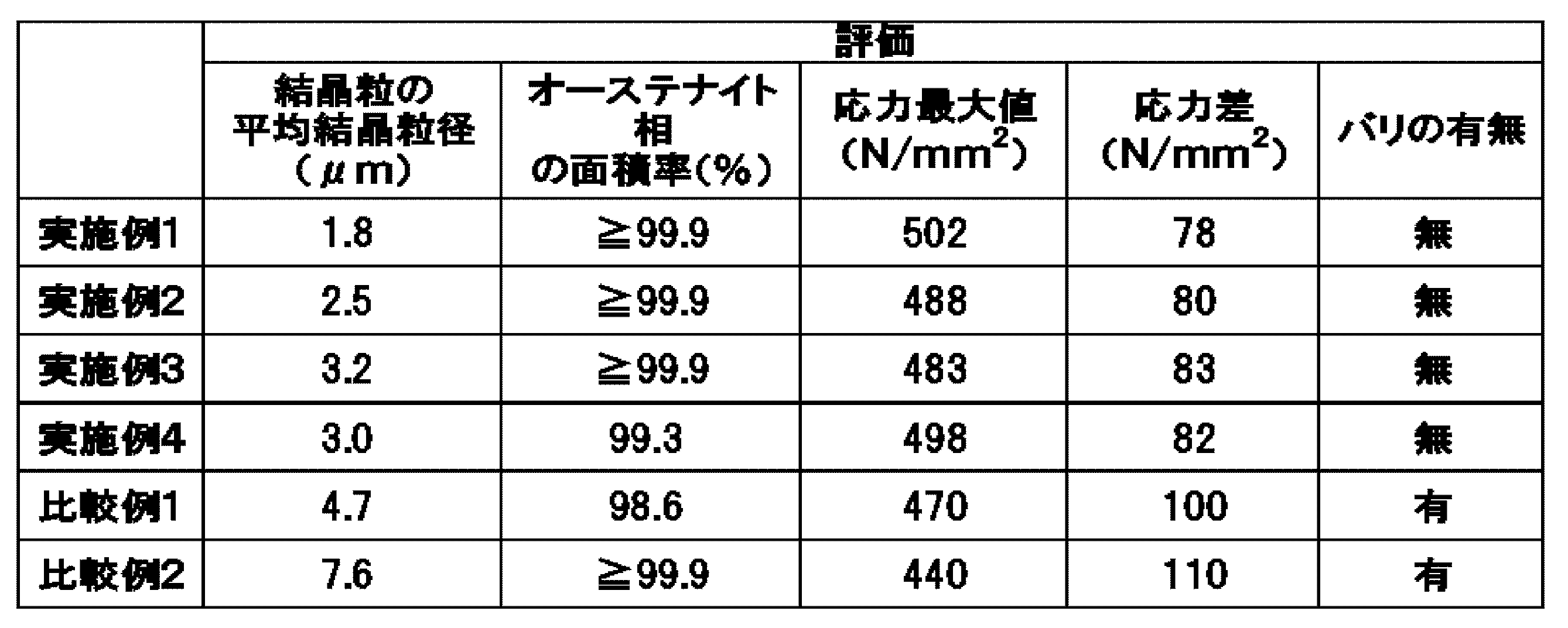
表2に示すように、実施例1~4のクラッド材は、そのコバール層表面におけるオーステナイト相の面積率が99.3%以上と高く、また、比較例1、2のクラッド材に比べて、平均結晶粒径が小さいコバール結晶粒でコバール層が構成されていた。また、プレス試験の結果、実施例1~4のクラッド材は、応力差が小さく、バリの発生も無いことから、良好なプレス打ち抜き加工性を示すことが確認された。
Claims (8)
- 銀系ロウ材層とコバール層を有する、電子部品の気密封止用クラッド材であって、
該コバール層の表面において、電子線後方散乱回折法による結晶相分布測定から算出される、コバール結晶粒の全面積中に占めるオーステナイト相の面積の割合が99.0~100.0%であり、かつ、該コバール結晶粒の平均結晶粒径が0.5~3.5μmである、電子部品の気密封止用クラッド材。 - シールリングを製造するために用いられる、請求項1に記載のクラッド材。
- 前記コバール層から前記銀系ロウ材層への打ち抜き加工に用いられる、請求項1又は2に記載のクラッド材。
- 銀系ロウ材層とコバール層を有する、電子部品の気密封止用クラッド材を打ち抜き加工して形成される気密封止材であって、
該コバール層の表面において、電子線後方散乱回折法による結晶相分布測定から算出される、コバール結晶粒の全面積中に占めるオーステナイト相の面積の割合が99.0~100.0%であり、かつ、該コバール結晶粒の平均結晶粒径が0.5~3.5μmである気密封止材。 - 前記コバール層から前記銀系ロウ材層へ打ち抜き加工して形成される請求項4に記載の気密封止材。
- 前記気密封止材が、シールリングである請求項4又は5に記載の気密封止材。
- 銀系ロウ材層とコバール層を有する、電子部品の気密封止用クラッド材の製造方法であって、
該銀系ロウ材層と該コバール層を接合して積層体を形成する第1の工程と、
該積層体を熱処理、冷間圧延する第2の工程と、
第2の工程に引き続いて再度、該積層体を熱処理する第3の工程と
を含む、電子部品の気密封止用クラッド材の製造方法。 - 第2の工程における熱処理を500~800℃の範囲で行い、第3の工程における熱処理を300~600℃の範囲で行う請求項7に記載の製造方法。
Priority Applications (3)
| Application Number | Priority Date | Filing Date | Title |
|---|---|---|---|
| KR1020167033063A KR102368282B1 (ko) | 2014-05-29 | 2015-05-18 | 전자 부품의 기밀 밀봉용 클래드재 및 그 제조 방법 |
| JP2016523428A JP6232496B2 (ja) | 2014-05-29 | 2015-05-18 | 電子部品の気密封止用クラッド材及びその製造方法 |
| CN201580028144.0A CN106413976B (zh) | 2014-05-29 | 2015-05-18 | 用于电子部件的气密密封的包层材料及其制造方法 |
Applications Claiming Priority (2)
| Application Number | Priority Date | Filing Date | Title |
|---|---|---|---|
| JP2014-110832 | 2014-05-29 | ||
| JP2014110832 | 2014-05-29 |
Publications (1)
| Publication Number | Publication Date |
|---|---|
| WO2015182415A1 true WO2015182415A1 (ja) | 2015-12-03 |
Family
ID=54698752
Family Applications (1)
| Application Number | Title | Priority Date | Filing Date |
|---|---|---|---|
| PCT/JP2015/064145 Ceased WO2015182415A1 (ja) | 2014-05-29 | 2015-05-18 | 電子部品の気密封止用クラッド材及びその製造方法 |
Country Status (5)
| Country | Link |
|---|---|
| JP (1) | JP6232496B2 (ja) |
| KR (1) | KR102368282B1 (ja) |
| CN (1) | CN106413976B (ja) |
| MY (1) | MY181337A (ja) |
| WO (1) | WO2015182415A1 (ja) |
Cited By (1)
| Publication number | Priority date | Publication date | Assignee | Title |
|---|---|---|---|---|
| JP2017204544A (ja) * | 2016-05-10 | 2017-11-16 | 太陽誘電株式会社 | 電子デバイスおよびその製造方法 |
Citations (5)
| Publication number | Priority date | Publication date | Assignee | Title |
|---|---|---|---|---|
| JPH10330841A (ja) * | 1997-05-29 | 1998-12-15 | Nikko Kinzoku Kk | Fe−Ni系合金薄板の製造方法 |
| JP2000168721A (ja) * | 1998-12-01 | 2000-06-20 | Senju Metal Ind Co Ltd | リッド供給材、リッド供給材の製造装置およびリッド供 給材の製造方法 |
| JP2002030393A (ja) * | 2000-07-17 | 2002-01-31 | Hitachi Metals Ltd | セラミックパッケージ封止用材料とその製造方法 |
| JP2004115905A (ja) * | 2002-09-30 | 2004-04-15 | Hitachi Metals Ltd | 低熱膨張合金及び低熱膨張合金板 |
| JP2006049595A (ja) * | 2004-08-05 | 2006-02-16 | Tanaka Kikinzoku Kogyo Kk | 銀ろうクラッド材並びにパッケージ封止用の蓋体及びリング体 |
Family Cites Families (2)
| Publication number | Priority date | Publication date | Assignee | Title |
|---|---|---|---|---|
| JPS531814A (en) | 1976-06-28 | 1978-01-10 | Toshiba Corp | Control unit of induction motor |
| CN103056500B (zh) * | 2012-11-30 | 2015-09-02 | 北京时代民芯科技有限公司 | 半导体陶瓷外壳封帽的焊接方法 |
-
2015
- 2015-05-18 MY MYPI2016704218A patent/MY181337A/en unknown
- 2015-05-18 CN CN201580028144.0A patent/CN106413976B/zh active Active
- 2015-05-18 JP JP2016523428A patent/JP6232496B2/ja active Active
- 2015-05-18 WO PCT/JP2015/064145 patent/WO2015182415A1/ja not_active Ceased
- 2015-05-18 KR KR1020167033063A patent/KR102368282B1/ko active Active
Patent Citations (5)
| Publication number | Priority date | Publication date | Assignee | Title |
|---|---|---|---|---|
| JPH10330841A (ja) * | 1997-05-29 | 1998-12-15 | Nikko Kinzoku Kk | Fe−Ni系合金薄板の製造方法 |
| JP2000168721A (ja) * | 1998-12-01 | 2000-06-20 | Senju Metal Ind Co Ltd | リッド供給材、リッド供給材の製造装置およびリッド供 給材の製造方法 |
| JP2002030393A (ja) * | 2000-07-17 | 2002-01-31 | Hitachi Metals Ltd | セラミックパッケージ封止用材料とその製造方法 |
| JP2004115905A (ja) * | 2002-09-30 | 2004-04-15 | Hitachi Metals Ltd | 低熱膨張合金及び低熱膨張合金板 |
| JP2006049595A (ja) * | 2004-08-05 | 2006-02-16 | Tanaka Kikinzoku Kogyo Kk | 銀ろうクラッド材並びにパッケージ封止用の蓋体及びリング体 |
Cited By (1)
| Publication number | Priority date | Publication date | Assignee | Title |
|---|---|---|---|---|
| JP2017204544A (ja) * | 2016-05-10 | 2017-11-16 | 太陽誘電株式会社 | 電子デバイスおよびその製造方法 |
Also Published As
| Publication number | Publication date |
|---|---|
| CN106413976B (zh) | 2021-10-26 |
| MY181337A (en) | 2020-12-21 |
| KR20170013243A (ko) | 2017-02-06 |
| JPWO2015182415A1 (ja) | 2017-04-20 |
| CN106413976A (zh) | 2017-02-15 |
| KR102368282B1 (ko) | 2022-02-28 |
| JP6232496B2 (ja) | 2017-11-15 |
Similar Documents
| Publication | Publication Date | Title |
|---|---|---|
| JP4327460B2 (ja) | 均一な集合組織を有する耐火金属板及び該板を製造する方法 | |
| JP4716520B2 (ja) | 圧延銅箔 | |
| JP5939370B1 (ja) | オーステナイト系ステンレス鋼板 | |
| TWI705148B (zh) | 銅合金板材及其製造方法 | |
| CN108136729A (zh) | 金属层叠材料及其制造方法 | |
| JP6378819B1 (ja) | Cu−Co−Si系銅合金板材および製造方法並びにその板材を用いた部品 | |
| JP6446011B2 (ja) | 放熱部品用銅合金板及び放熱部品 | |
| JPWO2018235862A1 (ja) | メタルマスク用薄板の製造方法及びメタルマスク用薄板 | |
| JP2018016823A (ja) | 放熱部材用銅合金板材およびその製造方法 | |
| KR101715532B1 (ko) | 구리 합금 및 그의 제조 방법 | |
| JP2018162518A (ja) | ベーパーチャンバー用銅合金板及びベーパーチャンバー | |
| TWI462787B (zh) | Rolled copper foil | |
| JP2003226966A (ja) | 大型ターゲット材 | |
| WO2018066414A1 (ja) | 放熱部品用銅合金板、放熱部品、及び放熱部品の製造方法 | |
| WO2016152648A1 (ja) | 放熱部品用銅合金板及び放熱部品 | |
| JP6232496B2 (ja) | 電子部品の気密封止用クラッド材及びその製造方法 | |
| TWI439331B (zh) | Rolled copper foil | |
| JP2010082688A (ja) | β型チタン合金板の製造方法及びβ型チタン合金板 | |
| KR102244229B1 (ko) | Fe-Ni계 합금 박판의 제조 방법 및 Fe-Ni계 합금 박판 | |
| WO2019198549A1 (ja) | 圧延接合体及び圧延接合体の製造方法 | |
| KR101716669B1 (ko) | 마그네슘 합금판의 제조방법 | |
| CN102573287B (zh) | 轧制铜箔 | |
| CN111918746B (zh) | 包层材料及其制造方法 | |
| JP5237867B2 (ja) | リードフレーム用Fe−Ni系合金材料およびその製造方法 | |
| WO2019244962A1 (ja) | Fe-Ni系合金薄板 |
Legal Events
| Date | Code | Title | Description |
|---|---|---|---|
| 121 | Ep: the epo has been informed by wipo that ep was designated in this application |
Ref document number: 15800497 Country of ref document: EP Kind code of ref document: A1 |
|
| ENP | Entry into the national phase |
Ref document number: 2016523428 Country of ref document: JP Kind code of ref document: A |
|
| ENP | Entry into the national phase |
Ref document number: 20167033063 Country of ref document: KR Kind code of ref document: A |
|
| NENP | Non-entry into the national phase |
Ref country code: DE |
|
| 122 | Ep: pct application non-entry in european phase |
Ref document number: 15800497 Country of ref document: EP Kind code of ref document: A1 |