WO2015182279A1 - 蒸着装置および蒸着方法 - Google Patents
蒸着装置および蒸着方法 Download PDFInfo
- Publication number
- WO2015182279A1 WO2015182279A1 PCT/JP2015/061829 JP2015061829W WO2015182279A1 WO 2015182279 A1 WO2015182279 A1 WO 2015182279A1 JP 2015061829 W JP2015061829 W JP 2015061829W WO 2015182279 A1 WO2015182279 A1 WO 2015182279A1
- Authority
- WO
- WIPO (PCT)
- Prior art keywords
- vapor deposition
- substrate
- deposition mask
- mask
- gap
- Prior art date
- Legal status (The legal status is an assumption and is not a legal conclusion. Google has not performed a legal analysis and makes no representation as to the accuracy of the status listed.)
- Ceased
Links
Images







Classifications
-
- C—CHEMISTRY; METALLURGY
- C23—COATING METALLIC MATERIAL; COATING MATERIAL WITH METALLIC MATERIAL; CHEMICAL SURFACE TREATMENT; DIFFUSION TREATMENT OF METALLIC MATERIAL; COATING BY VACUUM EVAPORATION, BY SPUTTERING, BY ION IMPLANTATION OR BY CHEMICAL VAPOUR DEPOSITION, IN GENERAL; INHIBITING CORROSION OF METALLIC MATERIAL OR INCRUSTATION IN GENERAL
- C23C—COATING METALLIC MATERIAL; COATING MATERIAL WITH METALLIC MATERIAL; SURFACE TREATMENT OF METALLIC MATERIAL BY DIFFUSION INTO THE SURFACE, BY CHEMICAL CONVERSION OR SUBSTITUTION; COATING BY VACUUM EVAPORATION, BY SPUTTERING, BY ION IMPLANTATION OR BY CHEMICAL VAPOUR DEPOSITION, IN GENERAL
- C23C14/00—Coating by vacuum evaporation, by sputtering or by ion implantation of the coating forming material
- C23C14/22—Coating by vacuum evaporation, by sputtering or by ion implantation of the coating forming material characterised by the process of coating
- C23C14/24—Vacuum evaporation
-
- C—CHEMISTRY; METALLURGY
- C23—COATING METALLIC MATERIAL; COATING MATERIAL WITH METALLIC MATERIAL; CHEMICAL SURFACE TREATMENT; DIFFUSION TREATMENT OF METALLIC MATERIAL; COATING BY VACUUM EVAPORATION, BY SPUTTERING, BY ION IMPLANTATION OR BY CHEMICAL VAPOUR DEPOSITION, IN GENERAL; INHIBITING CORROSION OF METALLIC MATERIAL OR INCRUSTATION IN GENERAL
- C23C—COATING METALLIC MATERIAL; COATING MATERIAL WITH METALLIC MATERIAL; SURFACE TREATMENT OF METALLIC MATERIAL BY DIFFUSION INTO THE SURFACE, BY CHEMICAL CONVERSION OR SUBSTITUTION; COATING BY VACUUM EVAPORATION, BY SPUTTERING, BY ION IMPLANTATION OR BY CHEMICAL VAPOUR DEPOSITION, IN GENERAL
- C23C14/00—Coating by vacuum evaporation, by sputtering or by ion implantation of the coating forming material
- C23C14/04—Coating on selected surface areas, e.g. using masks
- C23C14/042—Coating on selected surface areas, e.g. using masks using masks
-
- H—ELECTRICITY
- H05—ELECTRIC TECHNIQUES NOT OTHERWISE PROVIDED FOR
- H05B—ELECTRIC HEATING; ELECTRIC LIGHT SOURCES NOT OTHERWISE PROVIDED FOR; CIRCUIT ARRANGEMENTS FOR ELECTRIC LIGHT SOURCES, IN GENERAL
- H05B33/00—Electroluminescent light sources
- H05B33/10—Apparatus or processes specially adapted to the manufacture of electroluminescent light sources
-
- H—ELECTRICITY
- H10—SEMICONDUCTOR DEVICES; ELECTRIC SOLID-STATE DEVICES NOT OTHERWISE PROVIDED FOR
- H10K—ORGANIC ELECTRIC SOLID-STATE DEVICES
- H10K50/00—Organic light-emitting devices
-
- H—ELECTRICITY
- H10—SEMICONDUCTOR DEVICES; ELECTRIC SOLID-STATE DEVICES NOT OTHERWISE PROVIDED FOR
- H10K—ORGANIC ELECTRIC SOLID-STATE DEVICES
- H10K71/00—Manufacture or treatment specially adapted for the organic devices covered by this subclass
-
- H—ELECTRICITY
- H10—SEMICONDUCTOR DEVICES; ELECTRIC SOLID-STATE DEVICES NOT OTHERWISE PROVIDED FOR
- H10K—ORGANIC ELECTRIC SOLID-STATE DEVICES
- H10K71/00—Manufacture or treatment specially adapted for the organic devices covered by this subclass
- H10K71/10—Deposition of organic active material
- H10K71/16—Deposition of organic active material using physical vapour deposition [PVD], e.g. vacuum deposition or sputtering
- H10K71/166—Deposition of organic active material using physical vapour deposition [PVD], e.g. vacuum deposition or sputtering using selective deposition, e.g. using a mask
Definitions
- the present invention relates to a vapor deposition apparatus and a vapor deposition method.
- This application claims priority on May 30, 2014 based on Japanese Patent Application No. 2014-113468 for which it applied to Japan, and uses the content for it here.
- Patent Document 1 a method of performing deposition while moving a deposition source and a deposition mask relative to the substrate has been proposed (for example, Patent Document 1).
- this vapor deposition method since the entire surface of the substrate is vapor-deposited while moving the vapor deposition mask relative to the substrate in a stepwise manner (scanning), the size of the vapor deposition mask can be made smaller than that of the substrate. Therefore, the evaporation mask is less likely to be bent, and variations in film thickness are suppressed.
- One embodiment of the present invention has been made in view of the above circumstances, and an object thereof is to provide a vapor deposition apparatus and a vapor deposition method capable of suppressing both the variation in film thickness and the blurring of the vapor deposition pattern.
- the vapor deposition apparatus comprises: A substrate holding portion for holding a substrate; a vapor deposition mask disposed on one surface of the substrate; and a relative relationship between the vapor deposition mask and the substrate in a direction parallel to the one surface in a state where the vapor deposition mask and the substrate are separated from each other.
- a first moving device that changes the position in a stepwise manner, and before the relative movement between the deposition mask and the substrate by the first moving device starts, the deposition mask and the substrate are moved away from each other.
- the relative movement between the vapor deposition mask and the substrate is adjusted, and the relative movement between the vapor deposition mask and the substrate by the first moving device is stopped, the vapor deposition mask and the substrate are moved.
- a gap adjusting device that adjusts the gap between the deposition mask and the substrate, and the gap adjusting device and the front surface of the deposition mask.
- a shutter may be included that shields an emission path of the vapor deposition particles from the vapor deposition source toward the opening.
- the vapor deposition apparatus includes a temperature control means for lowering a vapor deposition temperature of the vapor deposition source when an injection path of the vapor deposition particles from the vapor deposition source toward the opening is shielded by the shutter. Can be included.
- the vapor deposition source and the substrate are arranged in a direction parallel to the one surface when the vapor deposition source supplies the vapor deposition particles to the one surface through the opening.
- a second moving device for relative movement may be included.
- the second moving device can relatively move the vapor deposition source and the substrate so that the vapor deposition source reciprocates as viewed from the substrate.
- the gap adjusting device can align the vapor deposition mask with respect to the substrate by rotating the vapor deposition mask around a rotation axis orthogonal to the one surface. .
- the vapor deposition mask is disposed on one surface side of the substrate, and the vapor deposition mask and the substrate are changed in steps in a direction parallel to the one surface.
- the injection path can be shielded.
- the vapor deposition temperature of the vapor deposition source can be lowered while the injection path of the vapor deposition particles is shielded.
- the vapor deposition source and the substrate can be relatively moved in a direction parallel to the one surface while the first step is performed.
- the relative movement can be performed such that the vapor deposition source reciprocates as viewed from the substrate.
- the vapor deposition mask is rotated around a rotation axis orthogonal to the one surface to align the vapor deposition mask with respect to the substrate. be able to.
- a vapor deposition apparatus and a vapor deposition method that can suppress both variations in film thickness and blurring of a vapor deposition pattern.
- FIG. 1 is a perspective view illustrating a vapor deposition apparatus according to this embodiment.
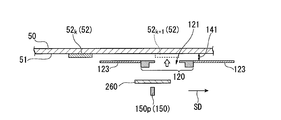
- 2 to 6 are schematic views for explaining the vapor deposition method according to the present embodiment.
- FIG. 7 is a diagram for explaining the flow of the vapor deposition method.
- the vapor deposition apparatus 100 includes a substrate holding unit 110, a vapor deposition mask 120, a first moving device 130, a gap adjusting device 140, a vapor deposition source 150, a shutter 160, and a temperature control unit 170. And a second moving device 180.
- the vapor deposition apparatus 100 deposits vapor deposition particles on the one surface 51 through the vapor deposition mask 120 while relatively moving the substrate 50 and the vapor deposition mask 120 in a direction parallel to the one surface 51 of the substrate 50.
- a method of performing vapor deposition on one surface 51 of the substrate 50 while relatively moving (scanning) the vapor deposition mask 120 and the substrate 50 is referred to as scan vapor deposition, and a direction SD in which the vapor deposition mask 120 moves relative to the substrate 50 is referred to as a scan direction. May be called.
- the substrate holding unit 110 holds the substrate 50 so that one surface 51 of the substrate 50 faces the vapor deposition source 150.
- the substrate holding unit 110 is, for example, an arm-shaped member that holds the substrate 50 horizontally, but the configuration of the substrate holding unit 110 is not limited thereto, and the substrate may be held by, for example, an electrostatic chuck mechanism.
- the active area 52 jk is an area where a vapor deposition pattern is formed, for example, an area corresponding to one panel of an organic EL display device.
- the one-dimensional array arranged in parallel with the scan direction SD is referred to as “row”, and the one-dimensional array arranged in parallel with the direction orthogonal to the scan direction SD (hereinafter referred to as “width direction”) is referred to as “column”.
- the number of rows in the array of the active area 52 jk is s, and the number of columns is t.
- the active area 52 jk is an active area arranged in the jth row and the kth column.
- the vapor deposition mask 120 is disposed on the one surface 51 side of the substrate 50.
- the vapor deposition mask 120 is provided with an opening 121.
- the opening 121 includes, for example, s pattern openings 121 1 to 121 s arranged in a line in the width direction.
- the shape of the pattern opening 121 j is a plurality of slits parallel to the scanning direction SD, but is not limited to this shape, and may be, for example, a slot shape.
- the size can be arranged. Since the vapor deposition mask 120 may be smaller than the substrate 50, even if the substrate 50 is enlarged, the vapor deposition mask is not easily bent. Therefore, variations in film thickness are suppressed.
- deposition plates 123 are provided at both ends of the vapor deposition mask 120 in the scanning direction SD.
- the deposition preventing plate 123 blocks a path through which the vapor deposition particles that reach the one surface 51 via the outside of the vapor deposition mask 120 fly. Thereby, the vapor deposition particles reach the one surface 51 only through the opening 121 of the vapor deposition mask 120. As a result, unnecessary vapor deposition particles that do not contribute to patterning can be prevented from being deposited on one surface 51.
- the first moving device 130 moves the vapor deposition mask 120 relative to the substrate 50 in the scanning direction SD.
- the first moving device 130 can be configured using a driving mechanism such as a ball screw, for example.
- the position of the substrate 50 is fixed, and the position of the vapor deposition mask 120 is moved by the first moving device 130.
- the position of the vapor deposition mask 120 may be fixed and the position of the substrate 50 may be moved by the first moving device 130, and both the positions of the vapor deposition mask 120 and the substrate 50 may be moved by the first moving device 130. It may be configured to be moved.
- the first moving device 130 operates in a state where the vapor deposition mask 120 and the substrate 50 are separated from each other so that the vapor deposition mask 120 and the substrate 50 do not come into contact with each other.
- the gap adjusting device 140 moves the vapor deposition mask 120 and the substrate 50 relative to each other in a direction approaching or separating from each other. Thereby, the gap 141 (see FIG. 2) between the vapor deposition mask 120 and the substrate 50 can be adjusted.
- the gap adjusting device 140 separates the vapor deposition mask 120 and the substrate 50 after the vapor deposition is completed in one active area row 52 k and before the vapor deposition mask 120 and the substrate 50 are relatively moved. Thereby, it can prevent that the vapor deposition mask 120 and the board
- the gap adjustment device 140 stops the relative movement between the vapor deposition mask 120 and the substrate 50 and brings the vapor deposition mask 120 and the substrate 50 close to each other before vapor deposition is performed in the active area row 52 k that is the movement destination. Thereby, it is suppressed that the edge of the vapor deposition film extends outside the edge of the pattern of the opening 121 of the vapor deposition mask 120 (pattern openings 121 1 to 121 s ), and blurring of the vapor deposition pattern is suppressed.
- the size of the gap 141 (see FIG. 2) during the relative movement of the deposition mask 120 and the substrate 50 is preferably 1 mm or more. There is no particular upper limit, but if the gap is increased too much, the gap adjustment time becomes longer and the tact time is worsened. On the other hand, the size of the gap 141 during vapor deposition is preferably 0.1 mm to 0.3 mm.
- the gap adjusting device 140 relatively moves the vapor deposition mask 120 and the substrate 50 in a direction perpendicular to the one surface 51.
- the gap adjusting device 140 can be configured using, for example, a driving mechanism such as an electric cylinder mechanism.
- the position of the substrate 50 is fixed, and the position of the vapor deposition mask 120 is moved by the gap adjusting device 140.
- the position of the vapor deposition mask 120 may be fixed and the position of the substrate 50 may be moved by the gap adjusting device 140, or the position of both the vapor deposition mask 120 and the substrate 50 may be moved by the gap adjusting device 140. .
- the gap adjusting device 140 includes, for example, a rotation mechanism that rotates the vapor deposition mask 120 around a rotation axis orthogonal to the one surface 51.
- a rotation mechanism that rotates the vapor deposition mask 120 around a rotation axis orthogonal to the one surface 51.
- the rotation mechanism for example, a known rotation mechanism used in a rotation stage or the like is used.
- the gap adjusting device 140 can align the deposition mask 120 with respect to the substrate 50 by rotating the deposition mask 120 around a rotation axis orthogonal to the one surface 51.
- the vapor deposition source 150 is adjusted after the gap 141 (see FIG. 2) between the vapor deposition mask 120 and the substrate 50 is adjusted by the gap adjusting device 140 being relatively moved in the direction in which the vapor deposition mask 120 and the substrate 50 are close to each other.
- the vapor deposition particles are supplied to one surface 51 of the substrate 50 through the opening 121 provided in the vapor deposition mask 120. As a result, a film of vapor deposition particles is formed on the one surface 51 exposed from the opening 121.
- the vapor deposition source 150 includes a nozzle unit 152 that ejects vapor deposition particles.
- the nozzle unit 152 includes, for example, s nozzles 152 1 to 152 s arranged in a line in the width direction.
- the s nozzles 152 1 to 152 s are provided in one-to-one correspondence with the s pattern openings 121 1 to 121 s , respectively.
- the injection path 151 is a set of paths through which individual vapor deposition particles fly.
- the flight path of each vapor deposition particle starts from the nozzle portion 152 of the vapor deposition source 150 and reaches a point in the opening 121 of the vapor deposition mask 120.
- injection is performed.
- a vapor deposition particle limiting unit 153 may be provided on the side facing the vapor deposition mask 120 of the vapor deposition source 150.
- the vapor deposition particle restriction unit 153 is fixed at a relative position in the vertical direction and the horizontal direction with respect to the vapor deposition source 150.
- the vapor deposition particle restriction unit 153 is provided with a plurality of through holes 154 through which vapor deposition particles pass.
- the vapor deposition particle restriction unit 153 includes, for example, s through holes 154 1 to 154 s arranged in a line in the width direction.
- the s through holes 154 1 to 154 s are provided in one-to-one correspondence with the s nozzles 152 1 to 152 s , respectively.
- the shutter 160 is a plate-like member that can be inserted between the vapor deposition mask 120 and the vapor deposition source 150.
- the shutter 160 has a gap 141 (see FIG. 2) between the vapor deposition mask 120 and the substrate 50 when the vapor deposition mask 120 and the substrate 50 are relatively moved by the first moving device 130, and by the gap adjusting device 140.
- the vapor deposition particle emission path 151 from the vapor deposition source 150 toward the opening 121 is shielded.
- vapor deposition can be performed on the substrate 50 only when the vapor deposition mask 120 and the substrate 50 are close to each other.
- the shutter 160 is provided between the vapor deposition mask 120 and the vapor deposition particle restriction unit 153, but may be provided between the vapor deposition particle restriction unit 153 and the nozzle unit 152.
- the length of the shutter 160 in the scanning direction SD is long enough to cover all the active area columns 52 1 to 52 t from the first column to the t-th column.
- the temperature control means 170 controls the temperature of the vapor deposition source 150.
- the temperature control unit 170 lowers the vapor deposition temperature of the vapor deposition source 150 when the ejection path 151 of vapor deposition particles from the vapor deposition source 150 toward the opening 121 is shielded by the shutter 160. Thereby, while vapor deposition is not performed on the substrate 50, flying of vapor deposition particles can be suppressed, and consumption of unnecessary vapor deposition material can be suppressed.
- the second moving device 180 moves the vapor deposition source 150 relative to the substrate 50 in the scanning direction SD.
- the second moving device 180 relatively moves the vapor deposition source 150 and the substrate 50 using a driving mechanism such as a ball screw.
- a driving mechanism such as a ball screw.
- the position of the substrate 50 is fixed, and the position of the vapor deposition source 150 is moved by the second moving device 180.
- the second moving device 180 relatively moves the vapor deposition source 150 and the substrate 50 in a direction parallel to the one surface 51 when the vapor deposition source 150 supplies the vapor deposition particles to the one surface 51 through the opening 121. Thereby, the dispersion
- the vapor deposition mask 120 is disposed on the one surface 51 side of the substrate 50, and the relative position between the vapor deposition mask 120 and the substrate 50 is changed stepwise in a direction parallel to the one surface 51.
- a plurality of vapor deposition pattern rows are sequentially formed on the one surface 51 by depositing vapor deposition particles on the one surface 51 through the first surface 51.
- the vapor deposition step (first step) S1 the determination step S2, the gap widening step (second step) S3, and the moving step (third step) S4.
- a gap reduction step (fourth step) S5 are sequentially performed.
- one deposition pattern row is formed on one surface 51 of the substrate 50 while fixing the relative position between the substrate 50 and the deposition mask 120.
- One vapor deposition pattern row includes s vapor deposition patterns. Each of the s vapor deposition patterns is a film of vapor deposition particles deposited through the s pattern openings 121 1 to 121 s .
- the relative position between the vapor deposition mask 120 and the substrate 50 is fixed.
- the size of the gap 141 between the vapor deposition mask 120 and the substrate 50 is set to be sufficiently small. Thereby, it can suppress that blur arises in the edge of a vapor deposition pattern.
- the deposition source 150 When the deposition for the k-th active area row 52 k starts, the deposition source 150 is located at the deposition start position 150 a for the k-th active area row 52 k .
- the shutter 160 is pulled out of the space between the vapor deposition mask 120 and the vapor deposition source 150 when vapor deposition on the k-th active area row 52 k starts. Thereby, the injection path from the vapor deposition source 150 to the opening 121 of the vapor deposition mask 120 is opened. As a result, the deposition for the active area row 52 k in the k-th row starts.
- the second moving device 180 moves the vapor deposition source 150 to the vapor deposition start position 150 a for the k-th active area row 52 k. from to evaporation end position 150b relative to the active area column 52 k of the k-th column, it is relatively moved in the scanning direction SD to the substrate 50.
- the shutter 160 is inserted into a space between the vapor deposition mask 120 and the vapor deposition source 150 located at the vapor deposition end position 150b. Thereby, the injection path from the vapor deposition source 150 to the opening 121 of the vapor deposition mask 120 is closed. As a result, the deposition step S1 for the kth active area row 52k is completed.
- the gap adjusting device 140 (see FIG. 1) separates the vapor deposition mask 120 and the substrate 50.
- the gap adjusting device 140 stops the relative movement between the vapor deposition mask 120 and the substrate 50.
- the second moving device 180 moves the vapor deposition source 150 relative to the substrate 50 in the scanning direction, as shown in FIG. 3. It may be moved relative to SD.
- the shutter 160 moves relative to the substrate 50 in the scanning direction SD following the vapor deposition source 150 so that the emission path from the vapor deposition source 150 to the opening 121 of the vapor deposition mask 120 is kept closed.
- the first mobile device 130 (see FIG. 1), the deposition mask 120, first through the opening 121 is an active area column 52 k a position facing the column k (k + 1)
- the substrate 50 is moved relative to the substrate 50 in the scanning direction SD to a position facing the active area row 52 k + 1 .
- the first moving device 130 stops the relative movement between the vapor deposition mask 120 and the substrate 50.
- the second moving device 180 scans the vapor deposition source 150 relative to the substrate 50 as shown in FIG.
- the relative movement may be performed in the direction SD.
- the shutter 160 moves relative to the substrate 50 in the scanning direction SD following the vapor deposition source 150 so that the emission path from the vapor deposition source 150 to the opening 121 of the vapor deposition mask 120 is kept closed.
- the gap adjusting device 140 brings the vapor deposition mask 120 and the substrate 50 close to each other.
- the gap adjusting device 140 stops the relative movement between the vapor deposition mask 120 and the substrate 50.
- the deposition mask 120 may be rotated around a rotation axis orthogonal to the one surface 51 and aligned with the substrate 50 in the gap reduction step S5.
- the second moving device 180 moves the vapor deposition source 150 relative to the substrate 50 in the scanning direction SD. Also good. In this case, the shutter 160 moves relative to the substrate 50 in the scanning direction SD following the vapor deposition source 150 so that the emission path from the vapor deposition source 150 to the opening 121 of the vapor deposition mask 120 is kept closed.
- the second moving device 180 moves the deposition source 150 relative to the substrate 50 in the scanning direction SD, and moves the deposition source 150 to the first level. (k + 1) to reach the deposition start position 150c relative to the active area column 52 k + 1 columns.
- the second moving device 180 moves the vapor deposition source 150 to the (k + 1) th active area column 52 k + 1 .
- the substrate 50 is moved relative to the substrate 50 in the scanning direction SD from the deposition start position 150c to the deposition end position 150d for the (k + 1) th active area row 52k + 1 .
- vapor deposition is performed from the active area column 52 1 of the first column to the active area column 52 t of the t column. Thereby, vapor deposition is completed in the whole area of the active area group 52.
- the vapor deposition source 150 has continued to move in the scanning direction SD, but is not limited to this mode.
- the deposition end position 150b relative to the active area column 52 k of the k rows, spaced from the substrate 50 of the deposition mask 120, movement in the scanning direction SD of the deposition mask 120, after the proximity to the substrate 50 of the deposition mask 120, the deposition source 150 from the deposition end position 150b relative to the active area column 52 k of the k-th column (k + 1) th row You may move to the vapor deposition start position 150c with respect to the active area row 52 k + 1 .
- the active area of the substrate 50 is rotationally symmetric with respect to the rotation axis orthogonal to the one surface 51 and the number t of active area columns is an even number
- the vapor deposition source 150 is moved in the scanning direction SD.
- the deposited active area row is switched from the first row to the t / 2th row to the (t / 2 + 1) th row to the tth row
- the substrate 50 is rotated 180 ° around the rotation axis orthogonal to the one surface 51. Rotate and reposition.
- the vapor deposition source 150 is moved in the direction opposite to the scan direction SD. Thereby, the moving range of the vapor deposition source 150 can be halved. As a result, the scale of the second moving device 180 can be reduced, and the equipment cost can be reduced.
- the temperature of the vapor deposition source 150 may be lowered using the temperature control means 170 while vapor deposition is not performed. Thereby, consumption of an unnecessary material can be suppressed.
- FIG. 8 is a perspective view illustrating the vapor deposition apparatus according to this embodiment.
- 9 to 13 are schematic views for explaining the vapor deposition method according to the present embodiment.
- the first moving device 230 moves the substrate 50 relative to the vapor deposition mask 120.
- the gap adjusting device 240 moves the substrate 50 close to or away from the vapor deposition mask 120.
- the second moving device 280 reciprocates the vapor deposition source 150 with respect to the vapor deposition mask 120.
- the shutter 260 has a shorter length in the scanning direction SD. In these points, the present embodiment is greatly different from the first embodiment.
- the vapor deposition apparatus 200 includes a substrate holding unit 110, a vapor deposition mask 120, a first moving device 230, a gap adjusting device 240, a vapor deposition source 150, a shutter 260, a temperature control unit 170, and a second moving device. 280.
- the first moving device 230 moves the substrate 50 relative to the vapor deposition mask 120 in the direction opposite to the scanning direction SD.
- the first moving device 230 can be configured using a driving mechanism such as a ball screw, for example.
- the position of the vapor deposition mask 120 is fixed, and the position of the substrate 50 is moved by the first moving device 230.
- the substrate 50 is moved by, for example, fixing the substrate 50 to the substrate holding unit 110 and moving the substrate 50 together with the substrate holding unit 110.
- the first moving device 230 operates in a state where the vapor deposition mask 120 and the substrate 50 are separated from each other so that the vapor deposition mask 120 and the substrate 50 do not come into contact with each other.
- k 1 to t
- the gap adjusting device 240 moves the vapor deposition mask 120 and the substrate 50 relative to each other in a direction approaching or separating from each other. As a result, the gap 141 (see FIG. 9) between the vapor deposition mask 120 and the substrate 50 can be adjusted.
- the gap adjusting device 240 separates the vapor deposition mask 120 and the substrate 50 after the vapor deposition is completed in one active area row 52 k and before the vapor deposition mask 120 and the substrate 50 are relatively moved. Thereby, it can prevent that the vapor deposition mask 120 and the board
- the gap adjusting device 240 brings the vapor deposition mask 120 and the substrate 50 close to each other before the relative movement between the vapor deposition mask 120 and the substrate 50 stops and vapor deposition is performed in the active area row 52 k that is the movement destination. Thereby, it is suppressed that the edge of the vapor deposition film extends outside the edge of the pattern of the opening 121 of the vapor deposition mask 120 (pattern openings 121 1 to 121 s ), and blurring of the vapor deposition pattern is suppressed.
- the size of the gap 141 (see FIG. 9) during the relative movement of the vapor deposition mask 120 and the substrate 50 is preferably 1 mm or more. There is no particular upper limit, but if the gap is increased too much, the gap adjustment time becomes longer and the tact time is worsened. On the other hand, the size of the gap 141 during vapor deposition is preferably 0.1 mm to 0.3 mm.
- the gap adjusting device 240 relatively moves the vapor deposition mask 120 and the substrate 50 in a direction perpendicular to the first surface 51.
- the gap adjusting device 240 can be configured using a drive mechanism such as an electric cylinder mechanism, for example.
- the position of the vapor deposition mask 120 is fixed, and the position of the substrate 50 is moved by the gap adjusting device 240.
- a configuration in which the position of the substrate 50 is fixed and the position of the vapor deposition mask 120 is moved by the gap adjusting device 240 or a position in which both the vapor deposition mask 120 and the substrate 50 are moved by the gap adjusting device 240 may be adopted. .
- the gap adjusting device 240 includes, for example, a rotation mechanism that rotates the vapor deposition mask 120 around a rotation axis orthogonal to the one surface 51.
- a rotation mechanism for example, a rotation mechanism used in a rotation stage or the like is used.
- the gap adjusting device 140 can align the deposition mask 120 with respect to the substrate 50 by rotating the deposition mask 120 around a rotation axis orthogonal to the one surface 51.
- the shutter 260 is a plate-like member that can be inserted between the vapor deposition mask 120 and the vapor deposition source 150.
- the shutter 260 has a gap 141 (see FIG. 9) between the vapor deposition mask 120 and the substrate 50 when the vapor deposition mask 120 and the substrate 50 are relatively moved by the first moving device 230 and by the gap adjusting device 240.
- the vapor deposition particle emission path 151 from the vapor deposition source 150 toward the opening 121 is shielded. Thereby, vapor deposition can be performed on the substrate 50 only when the vapor deposition mask 120 and the substrate 50 are close to each other. As a result, the blur of the vapor deposition pattern can be further suppressed.
- the second moving device 280 reciprocates the vapor deposition source 150 with respect to the substrate 50 in parallel with the scanning direction SD while vapor deposition is being performed.
- the second moving device 280 relatively moves the vapor deposition source 150 and the vapor deposition mask 120 using a drive mechanism such as a ball screw.
- the substrate 50 is stopped during vapor deposition, and the position of the vapor deposition source 150 is moved by the second moving device 180.
- the second moving device 280 relatively moves the vapor deposition source 150 and the substrate 50 in a direction parallel to the one surface 51 when the vapor deposition source 150 supplies the vapor deposition particles to the one surface 51 through the opening 121. Thereby, the dispersion
- the position of the vapor deposition mask 120 is fixed, and the position of the substrate 50 is moved by the first moving device 230. For this reason, the vapor deposition source 150 can reciprocate only in the vicinity of the position facing the fixed opening 121. As a result, the driving cost of the vapor deposition source 150 can be reduced.
- the length of the shutter 260 in the scanning direction SD is sufficient to cover one row in the active area group 52 of the substrate 50.
- the weight of the shutter 260 can be reduced, so that the shutter 260 can be prevented from being bent and the driving cost can be reduced.
- the vapor deposition mask 120 is disposed on the one surface 51 side of the substrate 50, and the relative position between the vapor deposition mask 120 and the substrate 50 is changed stepwise in a direction parallel to the one surface 51.
- a plurality of vapor deposition pattern rows are sequentially formed on the one surface 51 by depositing vapor deposition particles on the one surface 51 through the first surface 51.
- the vapor deposition step (first step) S1 the determination step S2, the gap widening step (second step) S3, and the moving step (third step) S4.
- a gap reduction step (fourth step) S5 are sequentially performed.
- the relative position between the vapor deposition mask 120 and the substrate 50 is fixed.
- the size of the gap 141 between the vapor deposition mask 120 and the substrate 50 is set to be sufficiently small. Thereby, it can suppress that blur arises in the edge of a vapor deposition pattern.
- the vapor deposition source 150 is located at the first position 150p.
- the shutter 260 is pulled out of the space between the vapor deposition mask 120 and the vapor deposition source 150. Thereby, the injection path from the vapor deposition source 150 to the opening 121 of the vapor deposition mask 120 is opened. As a result, the deposition for the active area row 52 k in the k-th row starts.
- the second moving device 280 moves the vapor deposition source 150 between the first position 150p and the second position 150q. Are reciprocated in parallel with the scanning direction SD with respect to the substrate 50.
- the vapor deposition source 150 moves relative to the substrate 50 while vapor deposition is performed.
- vapor deposition particles are deposited from various directions from the first position 150p to the second position 150q while vapor deposition is performed on the k-th active area row 52k.
- variations in film thickness can be suppressed and the film thickness can be made uniform.
- the shutter 260 is inserted into a space between the vapor deposition mask 120 and the vapor deposition source 150 located at the first position 150p. Thereby, the injection path from the vapor deposition source 150 to the opening 121 of the vapor deposition mask 120 is closed. As a result, the vapor deposition step (first step) S1 for the active area row 52k in the kth row is completed.
- the gap adjusting device 240 (see FIG. 8) separates the vapor deposition mask 120 and the substrate 50.
- the gap adjusting device 240 stops the relative movement between the vapor deposition mask 120 and the substrate 50.
- the first mobile device 230 (see FIG. 8) is a substrate 50, first the opening portion 121 is an active area column 52 k a position facing the column k (k + 1) columns Is moved relative to the vapor deposition mask 120 in a direction opposite to the scanning direction SD to a position facing the active area row 52 k + 1 .
- the first moving device 230 stops the relative movement between the vapor deposition mask 120 and the substrate 50.
- the gap adjusting device 240 brings the vapor deposition mask 120 and the substrate 50 close to each other.
- the gap adjusting device 240 stops the relative movement between the vapor deposition mask 120 and the substrate 50.
- the second moving device 280 moves the vapor deposition source 150 from the first position 150p to the second position 150q. Is reciprocated in parallel with the scanning direction SD with respect to the substrate 50.
- vapor deposition is performed from the active area column 52 1 of the first column to the active area column 52 t of the t column. Thereby, vapor deposition is completed in the whole area of the active area group 52.
- the vapor deposition source 150 has reciprocated between the first position 150p and the second position 150q.
- the present invention is not limited to this mode.
- the deposition source 150 moves from the first position 150p to the second position 150q in the scanning direction SD
- the vapor deposition source 150 may move from the second position 150q to the first position 150p in the direction opposite to the scan direction SD. Good. Thereby, the deposition time can be shortened while the uniformity of the film thickness remains the same as in the first embodiment.
- the temperature of the vapor deposition source 150 may be lowered using the temperature control means 170 while vapor deposition is not performed. Thereby, consumption of an unnecessary material can be suppressed.
- One embodiment of the present invention can be applied to a vapor deposition apparatus or the like that needs to suppress both variation in film thickness and blurring of a vapor deposition pattern.
Landscapes
- Chemical & Material Sciences (AREA)
- Engineering & Computer Science (AREA)
- Chemical Kinetics & Catalysis (AREA)
- Materials Engineering (AREA)
- Mechanical Engineering (AREA)
- Metallurgy (AREA)
- Organic Chemistry (AREA)
- Manufacturing & Machinery (AREA)
- Physics & Mathematics (AREA)
- Optics & Photonics (AREA)
- Electroluminescent Light Sources (AREA)
- Physical Vapour Deposition (AREA)
Abstract
蒸着マスク(120)と基板(50)とが離間した状態で一面(51)と平行な方向に蒸着マスク(120)と基板(50)との相対位置をステップ状に変化させる第一の移動装置(130)と、第一の移動装置(130)による蒸着マスク(120)と基板(50)との相対移動が開始する前に、蒸着マスク(120)と基板(50)とを互いに離間する方向に相対移動させ、蒸着マスク(120)と基板(50)との間のギャップを調整し、かつ、第一の移動装置(130)による蒸着マスク(120)と基板(50)との相対移動が停止したときに、蒸着マスク(120)と基板(50)とを互いに近接する方向に相対移動させ、蒸着マスク(120)と基板(50)との間の前記ギャップを調整するギャップ調整装置(140)と、を含む蒸着装置(100)。
Description
本発明は、蒸着装置および蒸着方法に関するものである。
本願は、2014年5月30日に、日本に出願された特願2014-113468号に基づき優先権を主張し、その内容をここに援用する。
本願は、2014年5月30日に、日本に出願された特願2014-113468号に基づき優先権を主張し、その内容をここに援用する。
真空蒸着法を用いた基板のパターニング方法のひとつとして、蒸着源と蒸着マスクとを基板に対して相対移動させながら蒸着を行う方法が提案されている(例えば、特許文献1)。この蒸着方法では、蒸着マスクを基板に対してステップ状に相対移動(スキャン)させながら、基板の全面を蒸着するので、蒸着マスクのサイズは基板よりも小さくすることができる。そのため、蒸着マスクの撓みが生じにくくなり、膜厚のバラツキが抑制される。
しかし、上述の蒸着方法では、基板に対して相対移動する蒸着マスクが基板と接触しないようにするために、蒸着マスクと基板とを十分に離間させる必要がある。蒸着粒子の一部は、基板の法線に対し有限の角度をもって基板に入射する。このため、蒸着マスクと基板とが離間していると、蒸着膜の縁は蒸着マスクの開口部のパターンの縁よりも外側に広がってしまう。その結果、蒸着パターンにボケが発生するという問題が生じる。
本発明の一態様は上記事情に鑑みてなされたものであって、膜厚のバラツキと蒸着パターンのボケとの両方を抑制できる蒸着装置および蒸着方法を提供することを目的とする。
本発明の第一の態様に係る蒸着装置は、
基板を保持する基板保持部と、前記基板の一面側に配置された蒸着マスクと、前記蒸着マスクと前記基板とが離間した状態で前記一面と平行な方向に前記蒸着マスクと前記基板との相対位置をステップ状に変化させる第一の移動装置と、前記第一の移動装置による前記蒸着マスクと前記基板との相対移動が開始する前に、前記蒸着マスクと前記基板とを互いに離間する方向に相対移動させ、前記蒸着マスクと前記基板との間のギャップを調整し、かつ、前記第一の移動装置による前記蒸着マスクと前記基板との相対移動が停止したときに、前記蒸着マスクと前記基板とを互いに近接する方向に相対移動させ、前記蒸着マスクと前記基板との間の前記ギャップを調整するギャップ調整装置と、前記ギャップ調整装置によって前記蒸着マスクと前記基板とが互いに近接する方向に相対移動させられて前記蒸着マスクと前記基板との間の前記ギャップが調整された後に、前記蒸着マスクに設けられた開口部を介して前記一面に蒸着粒子を供給し、前記開口部から露出した前記一面に前記蒸着粒子の膜を形成する蒸着源と、を含む。
基板を保持する基板保持部と、前記基板の一面側に配置された蒸着マスクと、前記蒸着マスクと前記基板とが離間した状態で前記一面と平行な方向に前記蒸着マスクと前記基板との相対位置をステップ状に変化させる第一の移動装置と、前記第一の移動装置による前記蒸着マスクと前記基板との相対移動が開始する前に、前記蒸着マスクと前記基板とを互いに離間する方向に相対移動させ、前記蒸着マスクと前記基板との間のギャップを調整し、かつ、前記第一の移動装置による前記蒸着マスクと前記基板との相対移動が停止したときに、前記蒸着マスクと前記基板とを互いに近接する方向に相対移動させ、前記蒸着マスクと前記基板との間の前記ギャップを調整するギャップ調整装置と、前記ギャップ調整装置によって前記蒸着マスクと前記基板とが互いに近接する方向に相対移動させられて前記蒸着マスクと前記基板との間の前記ギャップが調整された後に、前記蒸着マスクに設けられた開口部を介して前記一面に蒸着粒子を供給し、前記開口部から露出した前記一面に前記蒸着粒子の膜を形成する蒸着源と、を含む。
本発明の第一の態様に係る蒸着装置は、前記第一の移動装置によって前記蒸着マスクと前記基板とが相対移動しているときおよび前記ギャップ調整装置によって前記蒸着マスクと前記基板との間の前記ギャップが調整されているときに、前記蒸着源から前記開口部に向かう前記蒸着粒子の射出経路を遮蔽するシャッターを含むことができる。
本発明の第一の態様に係る蒸着装置は、前記シャッターによって前記蒸着源から前記開口部に向かう前記蒸着粒子の射出経路が遮蔽されているときに前記蒸着源の蒸着温度を下げる温度制御手段を含むことができる。
本発明の第一の態様に係る蒸着装置は、前記蒸着源が前記開口部を介して前記一面に前記蒸着粒子を供給しているときに前記蒸着源と前記基板とを前記一面と平行な方向に相対移動させる第二の移動装置を含むことができる。
本発明の第一の態様に係る蒸着装置は、前記第二の移動装置が、前記基板から見て前記蒸着源が往復移動するように前記蒸着源と前記基板とを相対移動させることができる。
本発明の第一の態様に係る蒸着装置は、前記ギャップ調整装置が、前記蒸着マスクを前記一面と直交する回転軸のまわりに回転させて前記蒸着マスクを前記基板に対してアラインメントすることができる。
本発明の第一の態様に係る蒸着方法は、基板の一面側に蒸着マスクを配置し、前記一面と平行な方向に前記蒸着マスクと前記基板との相対位置をステップ状に変化させながら前記蒸着マスクを介して前記一面に蒸着粒子を堆積させることにより、前記一面上に複数の蒸着パターン列を順次形成する蒸着方法であって、前記基板と前記蒸着マスクとの相対位置を固定して、前記蒸着マスクに設けられた開口部を介して前記一面に蒸着源から前記蒸着粒子を供給し、前記基板の一面上に1つの前記蒸着パターン列を形成する第1ステップと、前記第1ステップが終了した後に前記蒸着マスクと前記基板とを互いに離間する方向に相対移動させ、前記蒸着マスクと前記基板との間のギャップを調整する第2ステップと、前記蒸着マスクと前記基板とが離間した状態で前記一面と平行な方向に前記蒸着マスクと前記基板との相対位置を変化させる第3ステップと、前記蒸着マスクと前記基板との相対移動が停止したときに前記蒸着マスクと前記基板とを互いに近接する方向に相対移動させ、前記蒸着マスクと前記基板との間のギャップを調整する第4ステップと、を含む。
本発明の第一の態様に係る蒸着方法において、前記第2ステップ、前記第3ステップおよび前記第4ステップが行われる間、前記蒸着源から前記蒸着マスクに設けられた開口部に向かう前記蒸着粒子の射出経路を遮蔽することができる。
本発明の第一の態様に係る蒸着方法において、前記蒸着粒子の射出経路が遮蔽される間、蒸着源の蒸着温度を下げることができる。
本発明の第一の態様に係る蒸着方法において、前記第1ステップが行われる間、前記蒸着源と前記基板とを前記一面と平行な方向に相対移動させることができる。
本発明の第一の態様に係る蒸着方法において、前記相対移動は、前記基板から見て前記蒸着源が往復移動するように行うことができる。
本発明の第一の態様に係る蒸着方法において、前記第4ステップが行われる間、前記蒸着マスクを前記一面と直交する回転軸のまわりに回転させて前記蒸着マスクを前記基板に対してアラインメントすることができる。
本発明の一態様によれば、膜厚のバラツキと蒸着パターンのボケとの両方を抑制できる蒸着装置および蒸着方法を提供することができる。
[第一の実施形態]
以下、本発明の第一の実施形態について、図1から図6を用いて説明する。図1は、本実施形態に係る蒸着装置を説明する斜視図である。図2から図6は、本実施形態に係る蒸着方法を説明する模式図である。図7は、蒸着方法のフローを説明する図である。
以下、本発明の第一の実施形態について、図1から図6を用いて説明する。図1は、本実施形態に係る蒸着装置を説明する斜視図である。図2から図6は、本実施形態に係る蒸着方法を説明する模式図である。図7は、蒸着方法のフローを説明する図である。
(蒸着装置)
図1に示すように、蒸着装置100は、基板保持部110と、蒸着マスク120と、第一の移動装置130と、ギャップ調整装置140と、蒸着源150と、シャッター160と、温度制御手段170と、第二の移動装置180と、を含む。
図1に示すように、蒸着装置100は、基板保持部110と、蒸着マスク120と、第一の移動装置130と、ギャップ調整装置140と、蒸着源150と、シャッター160と、温度制御手段170と、第二の移動装置180と、を含む。
蒸着装置100は、基板50と蒸着マスク120とを基板50の一面51と平行な方向に相対移動させながら蒸着マスク120を介して一面51に蒸着粒子を堆積させる。以下、蒸着マスク120と基板50とを相対移動(スキャン)させながら基板50の一面51に蒸着を行う方法をスキャン蒸着と称し、蒸着マスク120が基板50に対して相対移動する方向SDをスキャン方向と称することがある。
基板保持部110は、基板50の一面51が蒸着源150と面するように、基板50を保持する。基板保持部110は、例えば、基板50を水平に保持するアーム状の部材であるが、基板保持部110の構成はこれに限定されず、例えば静電チャック機構で基板を保持しても良い。
基板50の一面51には、複数のアクティブエリア52jk(j=1~s,k=1~t。sは1以上の整数。tは2以上の整数)が、マトリクス状に配列されている。アクティブエリア52jkは、蒸着パターンが形成される領域であり、例えば有機ELディスプレイ装置の1枚分のパネルに相当する領域である。以下、スキャン方向SDに平行に並ぶ1次元配列を「行」、スキャン方向SDと直交する方向(以下、「幅方向」という。)に平行に並ぶ1次元配列を「列」という。アクティブエリア52jkの配列の行数はs、列数はtである。アクティブエリア52jkは、第j行第k列に配置されているアクティブエリアである。図1では、s=4,t=4の例を示すが、s,tはこれらの値に限られない。同じ行(第j行)に属するアクティブエリア52jk(k=1~t)は、すべて同じ形状である。
以下、同じ列(第k列)に属するアクティブエリア52jk(j=1~s)の集合を、アクティブエリア列52kと称する。また、全アクティブエリア52jk(j=1~s,k=1~t)の集合を、アクティブエリア群52と称することがある。
蒸着マスク120は、基板50の一面51側に配置される。蒸着マスク120には、開口部121が設けられる。開口部121は、例えば、幅方向に一列に配置されたs個のパターン開口1211~121sを含む。パターン開口121j(j=1~s)の形状は、第j行に属するアクティブエリア52jk(k=1~t)に形成される蒸着パターンの形状に対応する。図1では、パターン開口121jの形状は、スキャン方向SDに平行な複数のスリットであるが、この形状に限られるものではなく、例えばスロット形状でも良い。
蒸着マスク120のスキャン方向SDのサイズは、例えば、1列分のパターン開口121j(j=1~s)が配置できるサイズ、すなわち1列分のアクティブエリア52jk(k=1~t)が配置できるサイズとされる。蒸着マスク120が基板50よりも小さくてよいので、基板50が大型化しても、蒸着マスクの撓みが生じにくい。よって、膜厚のバラツキが抑制される。
蒸着マスク120のスキャン方向SDの両端には、例えば、防着板123が設けられる。防着板123は、蒸着マスク120の外側を経由して一面51に到達する蒸着粒子が飛翔する経路を遮断する。これにより、蒸着粒子は、蒸着マスク120の開口部121のみを経由して一面51に到達する。その結果、パターニングに寄与しない不要な蒸着粒子が一面51に堆積することを防止できる。
第一の移動装置130は、蒸着マスク120を基板50に対してスキャン方向SDに相対移動させる。第一の移動装置130は、例えば、ボールねじなどの駆動機構を用いて構成できる。本実施形態では、基板50の位置を固定し、蒸着マスク120の位置を第一の移動装置130によって移動させる構成となっている。しかし、蒸着マスク120の位置を固定し、基板50の位置を第一の移動装置130によって移動させる構成であってもよく、蒸着マスク120と基板50の双方の位置を第一の移動装置130によって移動させる構成であってもよい。
第一の移動装置130は、蒸着マスク120と基板50とが接触しないようにするため、蒸着マスク120と基板50とが離間した状態で作動する。第一の移動装置130は、複数のアクティブエリア列52k(k=1~t)が順次蒸着マスク120と対向するように、一面51と平行な方向に蒸着マスク120と基板50との相対位置をステップ状に変化させる。これにより、アクティブエリア列52kごとに、パターニングを行うことが可能となる。
ギャップ調整装置140は、蒸着マスク120と基板50とを、互いに近接または離間する方向に相対移動させる。これにより、蒸着マスク120と基板50との間のギャップ141(図2参照)を調整することが可能となる。
ギャップ調整装置140は、1つのアクティブエリア列52kで蒸着が終了した後、蒸着マスク120と基板50との相対移動が行われる前に、蒸着マスク120と基板50とを離間させる。これにより、蒸着マスク120と基板50とが相対移動する間、蒸着マスク120と基板50とが接触することを防ぐことができる。
ギャップ調整装置140は、蒸着マスク120と基板50との相対移動が停止し、移動先のアクティブエリア列52kで蒸着が行われる前に、蒸着マスク120と基板50とを互いに近接させる。これにより、蒸着膜の縁が蒸着マスク120の開口部121のパターン(パターン開口1211~121s)の縁よりも外側に広がることが抑制され、蒸着パターンのボケが抑制される。
蒸着マスク120と基板50とが相対移動する間のギャップ141(図2参照)の大きさは、1mm以上であることが好ましい。上限は特にないが、あまりギャップを大きくするとギャップ調整時間が長くなりタクトタイムを悪化させることになる。一方、蒸着中のギャップ141の大きさは、0.1mm~0.3mmであることが好ましい。
ギャップ調整装置140は、蒸着マスク120と基板50とを一面51と垂直な方向に相対移動させる。ギャップ調整装置140は、例えば、電動シリンダー機構などの駆動機構を用いて構成できる。本実施形態では、基板50の位置が固定され、蒸着マスク120の位置がギャップ調整装置140によって移動する構成となっている。しかし、蒸着マスク120の位置が固定され、基板50の位置がギャップ調整装置140によって移動する構成や、蒸着マスク120と基板50の双方の位置がギャップ調整装置140によって移動する構成であってもよい。
ギャップ調整装置140は、例えば、蒸着マスク120を一面51と直交する回転軸のまわりに回転させる回転機構を含む。回転機構としては、例えば、回転ステージなどで用いられる公知の回転機構が用いられる。ギャップ調整装置140は、蒸着マスク120を一面51と直交する回転軸のまわりに回転させて、基板50に対してアラインメントすることができる。
蒸着源150は、ギャップ調整装置140によって蒸着マスク120と基板50とが互いに近接する方向に相対移動させられて蒸着マスク120と基板50との間のギャップ141(図2参照)が調整された後に、蒸着マスク120に設けられた開口部121を介して基板50の一面51に蒸着粒子を供給する。これにより、開口部121から露出した一面51に、蒸着粒子の膜が形成される。
蒸着源150は、蒸着粒子を射出するノズル部152を含む。ノズル部152は、例えば、幅方向に一列に配置されたs個のノズル1521~152sを含む。s個のノズル1521~152sは、それぞれs個のパターン開口1211~121sと1対1に対応して設けられる。第j行のノズル121j(j=1~s)から射出された蒸着粒子は、第k列のアクティブエリア列52k(k=1~t)が蒸着されるときに、第j行のパターン開口121jを通過して第j行のアクティブエリア52jkに堆積する。これにより、第j行のパターン開口121jの形状に応じた蒸着パターンが、第j行のアクティブエリア52jkに形成される。
以下、蒸着源150のノズル部152と、蒸着マスク120の開口部121とを結ぶ領域を、射出経路151と称する。射出経路151は、個々の蒸着粒子が飛翔する経路の集合となっている。個々の蒸着粒子の飛翔経路は、蒸着源150のノズル部152から出発して、蒸着マスク120の開口部121内の点に到達する。本実施形態のように、蒸着源150がs個のノズル1521~152sを有し、これらに対応して、蒸着マスクがs個のパターン開口1211~121sを有する場合には、射出経路151はs個の錐状の領域となる。個々の錐状の領域は、1つのノズル152jを頂点としパターン開口121jを底面に持つ(j=1~s)。
蒸着源150の蒸着マスク120と対向する側には、例えば、蒸着粒子制限部153を設けてもよい。蒸着粒子制限部153は、蒸着源150に対して鉛直方向および水平方向の相対位置が固定される。蒸着粒子制限部153には、蒸着粒子が通過する複数の貫通穴154が設けられる。蒸着粒子制限部153は、例えば、幅方向に一列に配置されたs個の貫通穴1541~154sを含む。s個の貫通穴1541~154sは、それぞれs個のノズル1521~152sと1対1に対応して設けられる。これにより、各ノズル1521~152sから広角方向に射出された蒸着粒子のうち、貫通穴1541~154sを通過した蒸着粒子のみが、蒸着マスク120に到達する。これにより、蒸着粒子の射出方向の指向性が高まる。
シャッター160は、蒸着マスク120と蒸着源150との間に挿入可能な、板状の部材である。シャッター160は、第一の移動装置130によって蒸着マスク120と基板50とが相対移動しているとき、およびギャップ調整装置140によって蒸着マスク120と基板50との間のギャップ141(図2参照)が調整されているときに、蒸着源150から開口部121に向かう蒸着粒子の射出経路151を遮蔽する。これにより、蒸着マスク120と基板50とが互いに近接した状態にあるときに限り、基板50に蒸着を行うことができる。その結果、蒸着パターンのボケを、より抑制することができる。なお、図1ではシャッター160は蒸着マスク120と蒸着粒子制限部153との間に設けられているが、蒸着粒子制限部153とノズル部152との間に設けられていても良い。
シャッター160のスキャン方向SDの長さは、例えば、第1列から第t列までの全てのアクティブエリア列521~52tを覆うことのできる程度に十分長くなっている。第k列のアクティブエリア列52k(k=1~t)が蒸着マスク120の開口部121と対向した状態でギャップ141(図2参照)の調整が行われる間、シャッター160は第k列のアクティブエリア列52kを覆う位置まで挿入されている。これにより、第k列のアクティブエリア列52kに向かう蒸着粒子の射出経路151が遮蔽される。
温度制御手段170は、蒸着源150の温度を制御する。温度制御手段170は、例えば、シャッター160によって蒸着源150から開口部121に向かう蒸着粒子の射出経路151が遮蔽されているときに、蒸着源150の蒸着温度を下げる。これにより、基板50に蒸着が行われない間、蒸着粒子の飛翔を抑制し、不要な蒸着材料の消費を抑えることができる。
第二の移動装置180は、蒸着源150を基板50に対してスキャン方向SDに相対移動させる。第二の移動装置180は、例えば、ボールねじなどの駆動機構を用いて蒸着源150と基板50とを相対移動させる。本実施形態では、基板50の位置を固定し、蒸着源150の位置を第二の移動装置180によって移動させる構成となっている。
第二の移動装置180は、蒸着源150が開口部121を介して一面51に蒸着粒子を供給しているときに、蒸着源150と基板50とを一面51と平行な方向に相対移動させる。これにより、蒸着粒子の堆積速度が分布を有することに起因する膜厚のバラツキを抑制し、膜厚を均一化することができる。
(蒸着方法)
以下、図2から図7を用いて、本実施形態に係る蒸着方法を説明する。なお、図2から図6では、便宜上、基板保持部110、第一の移動装置130、ギャップ調整装置140、温度制御手段170、および第二の移動装置180の図示を省略している。
以下、図2から図7を用いて、本実施形態に係る蒸着方法を説明する。なお、図2から図6では、便宜上、基板保持部110、第一の移動装置130、ギャップ調整装置140、温度制御手段170、および第二の移動装置180の図示を省略している。
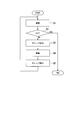
本実施形態に係る蒸着方法は、基板50の一面51側に蒸着マスク120を配置し、一面51と平行な方向に蒸着マスク120と基板50との相対位置をステップ状に変化させながら蒸着マスク120を介して一面51に蒸着粒子を堆積させることにより、一面51上に複数の蒸着パターン列を順次形成するものである。図7に示すように、本実施形態に係る蒸着方法では、蒸着ステップ(第1ステップ)S1と、判定ステップS2と、ギャップ拡大ステップ(第2ステップ)S3と、移動ステップ(第3ステップ)S4と、ギャップ縮小ステップ(第4ステップ)S5と、が順次行われる。
(第k列のアクティブエリア列に対する蒸着ステップS1)
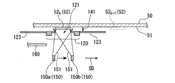
まず、図2に示すように、基板50と蒸着マスク120との相対位置を固定して基板50の一面51上に、1つの蒸着パターン列を形成する。図2は、例えば、第k列のアクティブエリア列52k(k=1~t-1)に蒸着パターン列を形成する例を示している。1つの蒸着パターン列には、s個の蒸着パターンが含まれる。s個の蒸着パターンは、それぞれs個のパターン開口1211~121sを介して堆積される蒸着粒子の膜である。蒸着を行う間、蒸着マスク120と基板50との相対位置は固定されている。蒸着を行う間、蒸着マスク120と基板50との間のギャップ141の大きさは、十分小さく設定されている。これにより、蒸着パターンの縁にボケが生じることを抑制できる。
まず、図2に示すように、基板50と蒸着マスク120との相対位置を固定して基板50の一面51上に、1つの蒸着パターン列を形成する。図2は、例えば、第k列のアクティブエリア列52k(k=1~t-1)に蒸着パターン列を形成する例を示している。1つの蒸着パターン列には、s個の蒸着パターンが含まれる。s個の蒸着パターンは、それぞれs個のパターン開口1211~121sを介して堆積される蒸着粒子の膜である。蒸着を行う間、蒸着マスク120と基板50との相対位置は固定されている。蒸着を行う間、蒸着マスク120と基板50との間のギャップ141の大きさは、十分小さく設定されている。これにより、蒸着パターンの縁にボケが生じることを抑制できる。
第k列のアクティブエリア列52kに対する蒸着が開始する時に、蒸着源150は第k列のアクティブエリア列52kに対する蒸着開始位置150aに位置している。第k列のアクティブエリア列52kに対する蒸着が開始する時に、シャッター160は、蒸着マスク120と蒸着源150との間の空間から引き抜かれる。これにより、蒸着源150から蒸着マスク120の開口部121に至る射出経路が開放される。その結果、第k列のアクティブエリア列52kに対する蒸着が開始する。
第k列のアクティブエリア列52kに対して蒸着が行われる間、第二の移動装置180(図1参照)は、蒸着源150を、第k列のアクティブエリア列52kに対する蒸着開始位置150aから第k列のアクティブエリア列52kに対する蒸着終了位置150bまで、基板50に対してスキャン方向SDに相対移動させる。
蒸着源150を基板50に対して固定した状態で蒸着を行う場合には、膜厚のバラツキが生ずる。この膜厚のバラツキは、蒸着粒子の入射角が基板50の一面51の中で分布を有するため、蒸着粒子の堆積速度も一面51の中で分布を有することに起因する。これに対し、本実施形態では、蒸着が行われる間、蒸着源150が基板50に対して、スキャン方向SDに相対移動する。これにより、第k列のアクティブエリア列52kに対して蒸着を行う間、蒸着開始位置150aから蒸着終了位置150bに至る様々な方向から蒸着粒子が堆積する。その結果、膜厚のバラツキを抑制し、膜厚を均一化することができる。
第k列のアクティブエリア列52kに対する蒸着が終了した時に、シャッター160は、蒸着マスク120と、蒸着終了位置150bに位置する蒸着源150との間の空間に挿入される。これにより、蒸着源150から蒸着マスク120の開口部121に至る射出経路が閉鎖される。その結果、第k列のアクティブエリア列52kに対する蒸着ステップS1が終了する。
(判定ステップS2)
図7に示すように、蒸着ステップS1が終了した時点で、第1列から第t列までのすべてのアクティブエリア列52k(k=1~t)に対して蒸着パターン列を形成し終えた場合は、全蒸着工程を終了する。そうでない場合は、ギャップ拡大ステップS3に移る。
図7に示すように、蒸着ステップS1が終了した時点で、第1列から第t列までのすべてのアクティブエリア列52k(k=1~t)に対して蒸着パターン列を形成し終えた場合は、全蒸着工程を終了する。そうでない場合は、ギャップ拡大ステップS3に移る。
(ギャップ拡大ステップS3)
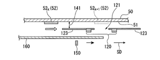
次に、図3に示すように、ギャップ調整装置140(図1参照)は、蒸着マスク120と基板50とを離間させる。蒸着マスク120と基板50との間のギャップ141が十分大きくなったところで、ギャップ調整装置140は蒸着マスク120と基板50との相対移動を停止する。ギャップ141を十分大きく設定することにより、後述の移動ステップS4において蒸着マスク120が基板50に対してスキャン方向SDに沿って相対移動する間、蒸着マスク120と基板50とが接触することを防止できる。
次に、図3に示すように、ギャップ調整装置140(図1参照)は、蒸着マスク120と基板50とを離間させる。蒸着マスク120と基板50との間のギャップ141が十分大きくなったところで、ギャップ調整装置140は蒸着マスク120と基板50との相対移動を停止する。ギャップ141を十分大きく設定することにより、後述の移動ステップS4において蒸着マスク120が基板50に対してスキャン方向SDに沿って相対移動する間、蒸着マスク120と基板50とが接触することを防止できる。
なお、ギャップ調整装置140が蒸着マスク120と基板50とを離間させる間、図3に示すように、第二の移動装置180(図1参照)は、蒸着源150を基板50に対してスキャン方向SDに相対移動させていてもよい。この場合、シャッター160は、蒸着源150から蒸着マスク120の開口部121に至る射出経路が閉鎖され続けるよう、蒸着源150に追随して、基板50に対してスキャン方向SDに相対移動する。
(移動ステップS4)
次に、図4に示すように、第一の移動装置130(図1参照)は、蒸着マスク120を、開口部121が第k列のアクティブエリア列52kと対向する位置から第(k+1)列のアクティブエリア列52k+1と対向する位置まで、基板50に対してスキャン方向SDに相対移動させる。蒸着マスク120が、開口部121が第(k+1)列のアクティブエリア列52k+1と対向する位置に到達した時、第一の移動装置130は蒸着マスク120と基板50との相対移動を停止する。
次に、図4に示すように、第一の移動装置130(図1参照)は、蒸着マスク120を、開口部121が第k列のアクティブエリア列52kと対向する位置から第(k+1)列のアクティブエリア列52k+1と対向する位置まで、基板50に対してスキャン方向SDに相対移動させる。蒸着マスク120が、開口部121が第(k+1)列のアクティブエリア列52k+1と対向する位置に到達した時、第一の移動装置130は蒸着マスク120と基板50との相対移動を停止する。
なお、蒸着マスク120が基板50に対してスキャン方向SDに相対移動する間、図4に示すように、第二の移動装置180(図1参照)は、蒸着源150を基板50に対してスキャン方向SDに相対移動させていてもよい。この場合、シャッター160は、蒸着源150から蒸着マスク120の開口部121に至る射出経路が閉鎖され続けるよう、蒸着源150に追随して、基板50に対してスキャン方向SDに相対移動する。
(ギャップ縮小ステップS5)
次に、図5に示すように、ギャップ調整装置140(図1参照)は、蒸着マスク120と基板50とを近接させる。蒸着マスク120と基板50との間のギャップ141が十分小さくなったところで、ギャップ調整装置140は蒸着マスク120と基板50との相対移動を停止する。ギャップ141を十分小さく設定することにより、蒸着パターンの縁にボケが生じることを抑制できる。
次に、図5に示すように、ギャップ調整装置140(図1参照)は、蒸着マスク120と基板50とを近接させる。蒸着マスク120と基板50との間のギャップ141が十分小さくなったところで、ギャップ調整装置140は蒸着マスク120と基板50との相対移動を停止する。ギャップ141を十分小さく設定することにより、蒸着パターンの縁にボケが生じることを抑制できる。
ギャップ調整装置140が回転機構を備える場合には、ギャップ縮小ステップS5において、蒸着マスク120を一面51と直交する回転軸のまわりに回転させて、基板50に対してアラインメントしてもよい。
蒸着マスク120と基板50とが近接する間、図5に示すように、第二の移動装置180(図1参照)は、蒸着源150を基板50に対してスキャン方向SDに相対移動させていてもよい。この場合、シャッター160は、蒸着源150から蒸着マスク120の開口部121に至る射出経路が閉鎖され続けるよう、蒸着源150に追随して、基板50に対してスキャン方向SDに相対移動する。
第(k+1)列のアクティブエリア列52k+1に対する蒸着が開始する時までに、第二の移動装置180は、蒸着源150を基板50に対してスキャン方向SDに相対移動させ、蒸着源150を第(k+1)列のアクティブエリア列52k+1に対する蒸着開始位置150cまで到達させる。
(第(k+1)列のアクティブエリア列に対する蒸着ステップS1)
次に、図6に示すように、第(k+1)列のアクティブエリア列52k+1に対して蒸着を行う。第(k+1)列のアクティブエリア列52k+1に対する蒸着が開始する時に、蒸着源150は第(k+1)列のアクティブエリア列52k+1に対する蒸着開始位置150cに位置している。第(k+1)列のアクティブエリア列52k+1に対する蒸着が開始する時に、シャッター160は、蒸着マスク120と蒸着源150との間の空間から引き抜かれる。これにより、蒸着源150から蒸着マスク120の開口部121に至る射出経路が開放される。その結果、第(k+1)列のアクティブエリア列52k+1に対する蒸着が開始する。
次に、図6に示すように、第(k+1)列のアクティブエリア列52k+1に対して蒸着を行う。第(k+1)列のアクティブエリア列52k+1に対する蒸着が開始する時に、蒸着源150は第(k+1)列のアクティブエリア列52k+1に対する蒸着開始位置150cに位置している。第(k+1)列のアクティブエリア列52k+1に対する蒸着が開始する時に、シャッター160は、蒸着マスク120と蒸着源150との間の空間から引き抜かれる。これにより、蒸着源150から蒸着マスク120の開口部121に至る射出経路が開放される。その結果、第(k+1)列のアクティブエリア列52k+1に対する蒸着が開始する。
第(k+1)列のアクティブエリア列52k+1に対して蒸着が行われる間、第二の移動装置180(図1参照)は、蒸着源150を、第(k+1)列のアクティブエリア列52k+1に対する蒸着開始位置150cから第(k+1)列のアクティブエリア列52k+1に対する蒸着終了位置150dまで、基板50に対してスキャン方向SDに相対移動させる。
以下、同様にして、第1列のアクティブエリア列521から第t列のアクティブエリア列52tまで蒸着を行う。これにより、アクティブエリア群52の全域において蒸着が完了する。
以上、第一の実施形態について説明した。なお、上述のギャップ拡大ステップS3からギャップ縮小ステップS5において、蒸着源150はスキャン方向SDに移動し続けていたが、この態様に限られるものではない。例えば、第k列のアクティブエリア列52kに対する蒸着が終了した時点で蒸着源150を第k列のアクティブエリア列52kに対する蒸着終了位置150bに停止させ、蒸着マスク120の基板50からの離間、蒸着マスク120のスキャン方向SDへの移動、蒸着マスク120の基板50への近接を行った後に、蒸着源150を第k列のアクティブエリア列52kに対する蒸着終了位置150bから第(k+1)列のアクティブエリア列52k+1に対する蒸着開始位置150cまで移動させてもよい。
また、例えば、基板50のアクティブエリアが一面51と直交する回転軸に対して回転対称であり、かつ、アクティブエリア列の数tが偶数の場合、まず、第1列から第t/2列までのアクティブエリア列521~52t/2に対しては、蒸着源150をスキャン方向SDに移動する。次に、蒸着されるアクティブエリア列が第1列~第t/2列から第(t/2+1)列~第t列に切り替わる間、基板50を一面51と直交する回転軸のまわりに180°回転させて配置し直す。最後に、第(t/2+1)列から第t列までのアクティブエリア列52t/2+1~52tに対しては、蒸着源150をスキャン方向SDと逆方向に移動する。これにより、蒸着源150の移動する範囲を半分にすることができる。
その結果、第二の移動装置180の規模を縮小でき、設備コストが低減できる。
その結果、第二の移動装置180の規模を縮小でき、設備コストが低減できる。
また、本実施形態において、蒸着が行われない間、温度制御手段170を用いて蒸着源150の温度を下げていてもよい。これにより、不要な材料の消費を抑制できる。
[第二の実施形態]
以下、本発明の第二の実施形態について、図7から図13を用いて説明する。図8は、本実施形態に係る蒸着装置を説明する斜視図である。図9から図13は、本実施形態に係る蒸着方法を説明する模式図である。
以下、本発明の第二の実施形態について、図7から図13を用いて説明する。図8は、本実施形態に係る蒸着装置を説明する斜視図である。図9から図13は、本実施形態に係る蒸着方法を説明する模式図である。
本実施形態においては、第一の移動装置230は、蒸着マスク120に対して基板50を相対移動させる。ギャップ調整装置240は、蒸着マスク120に対して基板50を近接または離間させる。第二の移動装置280は、蒸着マスク120に対して蒸着源150を往復移動させる。またシャッター260は、スキャン方向SDの長さがより短くなっている。これらの点において、本実施形態は第一の実施形態と大きく異なる。
(蒸着装置)
以下、本実施形態に係る蒸着装置200を、図8を用いて説明する。以下、図1から図6までと共通する構成要素には同じ符号を付し、説明を省略する。
以下、本実施形態に係る蒸着装置200を、図8を用いて説明する。以下、図1から図6までと共通する構成要素には同じ符号を付し、説明を省略する。
蒸着装置200は、基板保持部110と、蒸着マスク120と、第一の移動装置230と、ギャップ調整装置240と、蒸着源150と、シャッター260と、温度制御手段170と、第二の移動装置280と、を含む。
第一の移動装置230は、基板50を蒸着マスク120に対してスキャン方向SDと逆方向に相対移動させる。第一の移動装置230は、例えば、ボールねじなどの駆動機構を用いて構成できる。本実施形態では、蒸着マスク120の位置を固定し、基板50の位置を第一の移動装置230によって移動させる構成となっている。基板50の移動は、例えば、基板50を基板保持部110に固定し、基板50を基板保持部110とともに移動させて行う。
第一の移動装置230は、蒸着マスク120と基板50とが接触しないようにするため、蒸着マスク120と基板50とが離間した状態で作動する。第一の移動装置230は、複数のアクティブエリア列52k(k=1~t)が順次蒸着マスク120と対向するように、蒸着マスク120と基板50との相対位置をステップ状に変化させる。これにより、アクティブエリア列52kごとに、パターニングを行うことが可能となる。
ギャップ調整装置240は、蒸着マスク120と基板50とを、互いに近接または離間する方向に相対移動させる。これにより、蒸着マスク120と基板50との間のギャップ141(図9参照)を調整することが可能となる。
ギャップ調整装置240は、1つのアクティブエリア列52kで蒸着が終了した後、蒸着マスク120と基板50との相対移動が行われる前に、蒸着マスク120と基板50とを離間させる。これにより、蒸着マスク120と基板50とが相対移動する間、蒸着マスク120と基板50とが接触することを防ぐことができる。
ギャップ調整装置240は、蒸着マスク120と基板50との相対移動が停止し、移動先のアクティブエリア列52kで蒸着が行われる前に、蒸着マスク120と基板50とを互いに近接させる。これにより、蒸着膜の縁が蒸着マスク120の開口部121のパターン(パターン開口1211~121s)の縁よりも外側に広がることが抑制され、蒸着パターンのボケが抑制される。
蒸着マスク120と基板50とが相対移動する間のギャップ141(図9参照)の大きさは、1mm以上であることが好ましい。上限は特にないが、あまりギャップを大きくするとギャップ調整時間が長くなりタクトタイムを悪化させることになる。一方、蒸着中のギャップ141の大きさは、0.1mm~0.3mmであることが好ましい。
ギャップ調整装置240は、蒸着マスク120と基板50とを一面51と垂直な方向に相対移動させる。ギャップ調整装置240は、例えば、電動シリンダー機構などの駆動機構を用いて構成できる。本実施形態では、蒸着マスク120の位置が固定され、基板50の位置がギャップ調整装置240によって移動する構成となっている。しかし、基板50の位置が固定され、蒸着マスク120の位置がギャップ調整装置240によって移動する構成や、蒸着マスク120と基板50の双方の位置がギャップ調整装置240によって移動する構成であってもよい。
ギャップ調整装置240は、例えば、蒸着マスク120を一面51と直交する回転軸のまわりに回転させる回転機構を含む。回転機構としては、例えば、回転ステージなどで用いられる回転機構が用いられる。ギャップ調整装置140は、蒸着マスク120を一面51と直交する回転軸のまわりに回転させて、基板50に対してアラインメントすることができる。
シャッター260は、蒸着マスク120と蒸着源150との間に挿入可能な、板状の部材である。シャッター260は、第一の移動装置230によって蒸着マスク120と基板50とが相対移動しているとき、およびギャップ調整装置240によって蒸着マスク120と基板50との間のギャップ141(図9参照)が調整されているときに、蒸着源150から開口部121に向かう蒸着粒子の射出経路151を遮蔽する。これにより、蒸着マスク120と基板50とが互いに近接した状態にあるときに限り、基板50に蒸着を行うことができる。その結果、蒸着パターンのボケを、より抑制することができる。
第二の移動装置280は、蒸着が行われている間、蒸着源150を基板50に対してスキャン方向SDに平行に往復移動させる。第二の移動装置280は、例えば、ボールねじなどの駆動機構を用いて蒸着源150と蒸着マスク120とを相対移動させる。本実施形態では、蒸着中は基板50が停止しており、蒸着源150の位置を第二の移動装置180によって移動させる構成となっている。
第二の移動装置280は、蒸着源150が開口部121を介して一面51に蒸着粒子を供給しているときに、蒸着源150と基板50とを一面51と平行な方向に相対移動させる。これにより、蒸着粒子の堆積速度が分布を有することに起因する膜厚のバラツキを抑制し、膜厚を均一化することができる。
本実施形態では、蒸着マスク120の位置を固定し、基板50の位置を第一の移動装置230によって移動させる構成となっている。このため、蒸着源150は、固定された開口部121に対向する位置の近傍でのみ往復移動することができる。その結果、蒸着源150の駆動コストを減らすことができる。
また、本実施形態では、蒸着マスク120の位置を固定するため、シャッター260のスキャン方向SDの長さは、基板50のアクティブエリア群52内の一列を覆うことのできる程度の長さで足りる。その結果、シャッター260を軽量化することができるので、シャッター260の撓みを防いだり、駆動コストを減らしたりすることができる。
(蒸着方法)
以下、図7および図9から図13を用いて、本実施形態に係る蒸着方法を説明する。なお、図9から図12では、便宜上、基板保持部110、第一の移動装置230、ギャップ調整装置240、温度制御手段170、および第二の移動装置280の図示を省略している。
以下、図7および図9から図13を用いて、本実施形態に係る蒸着方法を説明する。なお、図9から図12では、便宜上、基板保持部110、第一の移動装置230、ギャップ調整装置240、温度制御手段170、および第二の移動装置280の図示を省略している。
本実施形態に係る蒸着方法は、基板50の一面51側に蒸着マスク120を配置し、一面51と平行な方向に蒸着マスク120と基板50との相対位置をステップ状に変化させながら蒸着マスク120を介して一面51に蒸着粒子を堆積させることにより、一面51上に複数の蒸着パターン列を順次形成するものである。図7に示すように、本実施形態に係る蒸着方法では、蒸着ステップ(第1ステップ)S1と、判定ステップS2と、ギャップ拡大ステップ(第2ステップ)S3と、移動ステップ(第3ステップ)S4と、ギャップ縮小ステップ(第4ステップ)S5と、が順次行われる。
(第k列のアクティブエリア列に対する蒸着ステップS1)
まず、図9に示すように、基板50と蒸着マスク120との相対位置を固定して基板50の一面51上に1つの蒸着パターン列を形成する。図9は、例えば、第k列のアクティブエリア列52k(k=1~t-1)に対して蒸着パターンを形成する例を示している。
蒸着を行う間、蒸着マスク120と基板50との相対位置は固定されている。蒸着を行う間、蒸着マスク120と基板50との間のギャップ141の大きさは、十分小さく設定されている。これにより、蒸着パターンの縁にボケが生じることを抑制できる。
まず、図9に示すように、基板50と蒸着マスク120との相対位置を固定して基板50の一面51上に1つの蒸着パターン列を形成する。図9は、例えば、第k列のアクティブエリア列52k(k=1~t-1)に対して蒸着パターンを形成する例を示している。
蒸着を行う間、蒸着マスク120と基板50との相対位置は固定されている。蒸着を行う間、蒸着マスク120と基板50との間のギャップ141の大きさは、十分小さく設定されている。これにより、蒸着パターンの縁にボケが生じることを抑制できる。
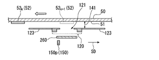
第k列のアクティブエリア列52kに対する蒸着が開始する時に、蒸着源150は第一の位置150pに位置している。アクティブエリア列52kに対する蒸着が開始する時に、シャッター260は、蒸着マスク120と蒸着源150との間の空間から引き抜かれる。これにより、蒸着源150から蒸着マスク120の開口部121に至る射出経路が開放される。その結果、第k列のアクティブエリア列52kに対する蒸着が開始する。
第k列のアクティブエリア列52kに対して蒸着が行われる間、第二の移動装置280(図8参照)は、蒸着源150を、第一の位置150pから第二の位置150qまでの区間を、基板50に対してスキャン方向SDに平行に往復移動させる。
本実施形態でも、蒸着が行われる間、蒸着源150が基板50に対して相対移動する。
これにより、第k列のアクティブエリア列52kに対して蒸着を行う間、第一の位置150pから第二の位置150qに至る様々な方向から蒸着粒子が堆積する。その結果、膜厚のバラツキを抑制し、膜厚を均一化することができる。
これにより、第k列のアクティブエリア列52kに対して蒸着を行う間、第一の位置150pから第二の位置150qに至る様々な方向から蒸着粒子が堆積する。その結果、膜厚のバラツキを抑制し、膜厚を均一化することができる。
第k列のアクティブエリア列52kに対する蒸着が終了した時に、シャッター260は、蒸着マスク120と、第一の位置150pに位置する蒸着源150との間の空間に挿入される。これにより、蒸着源150から蒸着マスク120の開口部121に至る射出経路が閉鎖される。その結果、第k列のアクティブエリア列52kに対する蒸着ステップ(第1ステップ)S1が終了する。
(判定ステップS2)
図7に示すように、蒸着ステップS1が終了した時点で、第1列から第t列までのすべてのアクティブエリア列52k(k=1~t)に対して蒸着パターン列を形成し終えた場合は、全蒸着工程を終了する。そうでない場合は、ギャップ拡大ステップS3に移る。
図7に示すように、蒸着ステップS1が終了した時点で、第1列から第t列までのすべてのアクティブエリア列52k(k=1~t)に対して蒸着パターン列を形成し終えた場合は、全蒸着工程を終了する。そうでない場合は、ギャップ拡大ステップS3に移る。
(ギャップ拡大ステップS3)
次に、図10に示すように、ギャップ調整装置240(図8参照)は、蒸着マスク120と基板50とを離間させる。蒸着マスク120と基板50との間のギャップ141が十分大きくなったところで、ギャップ調整装置240は蒸着マスク120と基板50との相対移動を停止する。ギャップ141を十分大きく設定することにより、後述の移動ステップS4において蒸着マスク120が基板50に対してスキャン方向SDに沿って相対移動する間、蒸着マスク120と基板50とが接触することを防止できる。
次に、図10に示すように、ギャップ調整装置240(図8参照)は、蒸着マスク120と基板50とを離間させる。蒸着マスク120と基板50との間のギャップ141が十分大きくなったところで、ギャップ調整装置240は蒸着マスク120と基板50との相対移動を停止する。ギャップ141を十分大きく設定することにより、後述の移動ステップS4において蒸着マスク120が基板50に対してスキャン方向SDに沿って相対移動する間、蒸着マスク120と基板50とが接触することを防止できる。
(移動ステップS4)
次に、図11に示すように、第一の移動装置230(図8参照)は、基板50を、開口部121が第k列のアクティブエリア列52kと対向する位置から第(k+1)列のアクティブエリア列52k+1と対向する位置まで、蒸着マスク120に対してスキャン方向SDと逆方向に相対移動させる。蒸着マスク120が、開口部121が第(k+1)列のアクティブエリア列52k+1と対向する位置に到達した時、第一の移動装置230は蒸着マスク120と基板50との相対移動を停止する。
次に、図11に示すように、第一の移動装置230(図8参照)は、基板50を、開口部121が第k列のアクティブエリア列52kと対向する位置から第(k+1)列のアクティブエリア列52k+1と対向する位置まで、蒸着マスク120に対してスキャン方向SDと逆方向に相対移動させる。蒸着マスク120が、開口部121が第(k+1)列のアクティブエリア列52k+1と対向する位置に到達した時、第一の移動装置230は蒸着マスク120と基板50との相対移動を停止する。
(ギャップ縮小ステップS5)
次に、図12に示すように、ギャップ調整装置240(図8参照)は、蒸着マスク120と基板50とを近接させる。蒸着マスク120と基板50との間のギャップ141が十分小さくなったところで、ギャップ調整装置240は蒸着マスク120と基板50との相対移動を停止する。ギャップ141を十分小さく設定することにより、蒸着パターンの縁にボケが生じることを抑制できる。
次に、図12に示すように、ギャップ調整装置240(図8参照)は、蒸着マスク120と基板50とを近接させる。蒸着マスク120と基板50との間のギャップ141が十分小さくなったところで、ギャップ調整装置240は蒸着マスク120と基板50との相対移動を停止する。ギャップ141を十分小さく設定することにより、蒸着パターンの縁にボケが生じることを抑制できる。
(第(k+1)列のアクティブエリア列に対する蒸着ステップS1)
次に、図13に示すように、第(k+1)列のアクティブエリア列52k+1に対して蒸着を行う。第(k+1)列のアクティブエリア列52k+1に対する蒸着が開始する時に、蒸着源150は第一の位置150pに位置している。第(k+1)列のアクティブエリア列52k+1に対する蒸着が開始する時に、シャッター260は、蒸着マスク120と蒸着源150との間の空間から引き抜かれる。これにより、蒸着源150から蒸着マスク120の開口部121に至る射出経路が開放される。その結果、第(k+1)列のアクティブエリア列52k+1に対する蒸着が開始する。
次に、図13に示すように、第(k+1)列のアクティブエリア列52k+1に対して蒸着を行う。第(k+1)列のアクティブエリア列52k+1に対する蒸着が開始する時に、蒸着源150は第一の位置150pに位置している。第(k+1)列のアクティブエリア列52k+1に対する蒸着が開始する時に、シャッター260は、蒸着マスク120と蒸着源150との間の空間から引き抜かれる。これにより、蒸着源150から蒸着マスク120の開口部121に至る射出経路が開放される。その結果、第(k+1)列のアクティブエリア列52k+1に対する蒸着が開始する。
第(k+1)列のアクティブエリア列52k+1に対して蒸着が行われる間、第二の移動装置280(図8参照)は、蒸着源150を、第一の位置150pから第二の位置150qまでの区間を、基板50に対してスキャン方向SDに平行に往復移動させる。
以下、同様にして、第1列のアクティブエリア列521から第t列のアクティブエリア列52tまで蒸着を行う。これにより、アクティブエリア群52の全域において蒸着が完了する。
以上、第二の実施形態について説明した。なお、上述の蒸着ステップS1において、蒸着源150は第一の位置150pと第二の位置150qの間を往復移動していたが、この態様に限られるものではない。例えば、第k列のアクティブエリア列52k(kは奇数)に対して蒸着が行われるときは、蒸着源150は第一の位置150pから第二の位置150qまでスキャン方向SDに移動し、第k列のアクティブエリア列52k(kは偶数)に対して蒸着が行われるときは、蒸着源150は第二の位置150qから第一の位置150pまでスキャン方向SDと逆方向に移動してもよい。これにより、膜厚の均一性は第一の実施形態と同等のまま、蒸着時間を短縮できる。
また、本実施形態において、蒸着が行われない間、温度制御手段170を用いて蒸着源150の温度を下げていてもよい。これにより、不要な材料の消費を抑制できる。
以上、添付図面を参照しながら本発明に係る好適な実施の形態例について説明したが、本発明は係る例に限定されないことは言うまでもない。上述した例において示した各構成部材の諸形状や組み合わせ等は一例であって、本発明の主旨から逸脱しない範囲において設計要求等に基づき種々変更可能である。
本発明の一態様は、膜厚のバラツキと蒸着パターンのボケとの両方を抑制することが必要な蒸着装置などに適用することができる。
100,200…蒸着装置、110…基板保持部、120…蒸着マスク、121…開口部、130,230…第一の移動装置、140,240…ギャップ調整装置、141…ギャップ、150…蒸着源、151…射出経路、160,260…シャッター、170…温度制御手段、180,280…第二の移動装置、50…基板、51…一面、S1…第1ステップ、S3…第二ステップ、S4…第3ステップ、S5…第4ステップ
Claims (12)
- 基板を保持する基板保持部と、
前記基板の一面側に配置された蒸着マスクと、
前記蒸着マスクと前記基板とが離間した状態で前記一面と平行な方向に前記蒸着マスクと前記基板との相対位置をステップ状に変化させる第一の移動装置と、
前記第一の移動装置による前記蒸着マスクと前記基板との相対移動が開始する前に、前記蒸着マスクと前記基板とを互いに離間する方向に相対移動させ、前記蒸着マスクと前記基板との間のギャップを調整し、かつ、前記第一の移動装置による前記蒸着マスクと前記基板との相対移動が停止したときに、前記蒸着マスクと前記基板とを互いに近接する方向に相対移動させ、前記蒸着マスクと前記基板との間の前記ギャップを調整するギャップ調整装置と、
前記ギャップ調整装置によって前記蒸着マスクと前記基板とが互いに近接する方向に相対移動させられて前記蒸着マスクと前記基板との間の前記ギャップが調整された後に、前記蒸着マスクに設けられた開口部を介して前記一面に蒸着粒子を供給し、前記開口部から露出した前記一面に前記蒸着粒子の膜を形成する蒸着源と、
を含む蒸着装置。 - 前記第一の移動装置によって前記蒸着マスクと前記基板とが相対移動しているときおよび前記ギャップ調整装置によって前記蒸着マスクと前記基板との間の前記ギャップが調整されているときに、前記蒸着源から前記開口部に向かう前記蒸着粒子の射出経路を遮蔽するシャッターを含む
請求項1に記載の蒸着装置。 - 前記シャッターによって前記蒸着源から前記開口部に向かう前記蒸着粒子の射出経路が遮蔽されているときに前記蒸着源の蒸着温度を下げる温度制御手段を含む
請求項2に記載の蒸着装置。 - 前記蒸着源が前記開口部を介して前記一面に前記蒸着粒子を供給しているときに前記蒸着源と前記基板とを前記一面と平行な方向に相対移動させる第二の移動装置を含む
請求項1から3のいずれか1項に記載の蒸着装置。 - 前記第二の移動装置は、前記基板から見て前記蒸着源が往復移動するように前記蒸着源と前記基板とを相対移動させる
請求項4に記載の蒸着装置。 - 前記ギャップ調整装置は、前記蒸着マスクを前記一面と直交する回転軸のまわりに回転させて前記蒸着マスクを前記基板に対してアラインメントする
請求項1から5のいずれか1項に記載の蒸着装置。 - 基板の一面側に蒸着マスクを配置し、前記一面と平行な方向に前記蒸着マスクと前記基板との相対位置をステップ状に変化させながら前記蒸着マスクを介して前記一面に蒸着粒子を堆積させることにより、前記一面上に複数の蒸着パターン列を順次形成する蒸着方法であって、
前記基板と前記蒸着マスクとの相対位置を固定して、前記蒸着マスクに設けられた開口部を介して前記一面に蒸着源から前記蒸着粒子を供給し、前記一面上に1つの前記蒸着パターン列を形成する第1ステップと、
前記第1ステップが終了した後に前記蒸着マスクと前記基板とを互いに離間する方向に相対移動させ、前記蒸着マスクと前記基板との間のギャップを調整する第2ステップと、
前記蒸着マスクと前記基板とが離間した状態で前記一面と平行な方向に前記蒸着マスクと前記基板との相対位置を変化させる第3ステップと、
前記蒸着マスクと前記基板との相対移動が停止したときに前記蒸着マスクと前記基板とを互いに近接する方向に相対移動させ、前記蒸着マスクと前記基板との間のギャップを調整する第4ステップと、を含む
蒸着方法。 - 前記第2ステップ、前記第3ステップおよび前記第4ステップが行われる間、前記蒸着源から前記蒸着マスクに設けられた開口部に向かう前記蒸着粒子の射出経路を遮蔽する
請求項7に記載の蒸着方法。 - 前記蒸着粒子の射出経路が遮蔽される間、前記蒸着源の蒸着温度を下げる
請求項8に記載の蒸着方法。 - 前記第1ステップが行われる間、前記蒸着源と前記基板とを前記一面と平行な方向に相対移動させる
請求項7から9のいずれか1項に記載の蒸着方法。 - 前記相対移動は、前記基板から見て前記蒸着源が往復移動するように行う
請求項10に記載の蒸着方法。 - 前記第4ステップが行われる間、前記蒸着マスクを前記一面と直交する回転軸のまわりに回転させて前記蒸着マスクを前記基板に対してアラインメントする
請求項7から11のいずれか1項に記載の蒸着方法。
Priority Applications (1)
| Application Number | Priority Date | Filing Date | Title |
|---|---|---|---|
| US15/314,629 US20170198384A1 (en) | 2014-05-30 | 2015-04-17 | Deposition apparatus and deposition method |
Applications Claiming Priority (2)
| Application Number | Priority Date | Filing Date | Title |
|---|---|---|---|
| JP2014113468 | 2014-05-30 | ||
| JP2014-113468 | 2014-05-30 |
Publications (1)
| Publication Number | Publication Date |
|---|---|
| WO2015182279A1 true WO2015182279A1 (ja) | 2015-12-03 |
Family
ID=54698620
Family Applications (1)
| Application Number | Title | Priority Date | Filing Date |
|---|---|---|---|
| PCT/JP2015/061829 Ceased WO2015182279A1 (ja) | 2014-05-30 | 2015-04-17 | 蒸着装置および蒸着方法 |
Country Status (3)
| Country | Link |
|---|---|
| US (1) | US20170198384A1 (ja) |
| TW (1) | TW201546305A (ja) |
| WO (1) | WO2015182279A1 (ja) |
Cited By (1)
| Publication number | Priority date | Publication date | Assignee | Title |
|---|---|---|---|---|
| JP2023006678A (ja) * | 2021-06-30 | 2023-01-18 | キヤノントッキ株式会社 | 成膜装置及び成膜方法 |
Families Citing this family (2)
| Publication number | Priority date | Publication date | Assignee | Title |
|---|---|---|---|---|
| JP2017150017A (ja) * | 2016-02-23 | 2017-08-31 | 株式会社ジャパンディスプレイ | 蒸着マスクの製造方法及び有機elディスプレイの製造方法 |
| CN110473822B (zh) * | 2018-05-09 | 2021-11-23 | 京东方科技集团股份有限公司 | 对位方法及对位装置、蒸镀设备 |
Citations (6)
| Publication number | Priority date | Publication date | Assignee | Title |
|---|---|---|---|---|
| JP2008088465A (ja) * | 2006-09-29 | 2008-04-17 | Seiko Epson Corp | 蒸着装置および有機エレクトロルミネッセンス装置の製造方法 |
| WO2009107733A1 (ja) * | 2008-02-26 | 2009-09-03 | 株式会社アルバック | 成膜源、蒸着装置、有機el素子の製造装置 |
| JP2011117083A (ja) * | 1999-12-27 | 2011-06-16 | Semiconductor Energy Lab Co Ltd | 発光装置の作製方法 |
| WO2012098994A1 (ja) * | 2011-01-18 | 2012-07-26 | シャープ株式会社 | 被成膜基板、有機el表示装置 |
| JP2013055039A (ja) * | 2011-08-11 | 2013-03-21 | Canon Inc | El発光装置の製造方法および蒸着装置 |
| JP2013147715A (ja) * | 2012-01-20 | 2013-08-01 | V Technology Co Ltd | マスク成膜装置及びマスク成膜方法 |
-
2015
- 2015-04-17 WO PCT/JP2015/061829 patent/WO2015182279A1/ja not_active Ceased
- 2015-04-17 US US15/314,629 patent/US20170198384A1/en not_active Abandoned
- 2015-04-28 TW TW104113575A patent/TW201546305A/zh unknown
Patent Citations (6)
| Publication number | Priority date | Publication date | Assignee | Title |
|---|---|---|---|---|
| JP2011117083A (ja) * | 1999-12-27 | 2011-06-16 | Semiconductor Energy Lab Co Ltd | 発光装置の作製方法 |
| JP2008088465A (ja) * | 2006-09-29 | 2008-04-17 | Seiko Epson Corp | 蒸着装置および有機エレクトロルミネッセンス装置の製造方法 |
| WO2009107733A1 (ja) * | 2008-02-26 | 2009-09-03 | 株式会社アルバック | 成膜源、蒸着装置、有機el素子の製造装置 |
| WO2012098994A1 (ja) * | 2011-01-18 | 2012-07-26 | シャープ株式会社 | 被成膜基板、有機el表示装置 |
| JP2013055039A (ja) * | 2011-08-11 | 2013-03-21 | Canon Inc | El発光装置の製造方法および蒸着装置 |
| JP2013147715A (ja) * | 2012-01-20 | 2013-08-01 | V Technology Co Ltd | マスク成膜装置及びマスク成膜方法 |
Cited By (2)
| Publication number | Priority date | Publication date | Assignee | Title |
|---|---|---|---|---|
| JP2023006678A (ja) * | 2021-06-30 | 2023-01-18 | キヤノントッキ株式会社 | 成膜装置及び成膜方法 |
| JP7755400B2 (ja) | 2021-06-30 | 2025-10-16 | キヤノントッキ株式会社 | 成膜装置及び成膜方法 |
Also Published As
| Publication number | Publication date |
|---|---|
| TW201546305A (zh) | 2015-12-16 |
| US20170198384A1 (en) | 2017-07-13 |
Similar Documents
| Publication | Publication Date | Title |
|---|---|---|
| KR102377183B1 (ko) | 고정밀 섀도 마스크 증착 시스템 및 그 방법 | |
| US8568963B2 (en) | Method of manufacturing mask for depositing thin film | |
| KR101634922B1 (ko) | 제한판 유닛 및 증착 유닛과 증착 장치 | |
| KR101442939B1 (ko) | 증착장치 및 증착방법 | |
| JPWO2016171075A1 (ja) | 蒸着装置および蒸着方法 | |
| WO2012099012A1 (ja) | 坩堝および蒸着装置 | |
| KR102124426B1 (ko) | 진공 증착 장치 및 이를 이용한 진공 증착 방법 | |
| KR102201107B1 (ko) | 증착 장치 및 이를 이용한 마스크 조립체의 정렬 방법 | |
| WO2014119452A1 (ja) | 蒸着ユニットおよび蒸着装置 | |
| KR20160041976A (ko) | 증착 장치 및 유기 일렉트로 루미네센스 소자의 제조 방법 | |
| WO2015182279A1 (ja) | 蒸着装置および蒸着方法 | |
| KR20140022804A (ko) | 증착 장치, 증착 방법, 유기 el 디스플레이 및 조명 장치 | |
| US9773600B2 (en) | Magnet plate assembly, deposition apparatus including the same, and deposition method using the same | |
| WO2016136595A1 (ja) | 蒸着ユニット、蒸着装置、および蒸着方法 | |
| US10087516B2 (en) | Evaporation apparatus and evaporation method | |
| JP4679912B2 (ja) | パターン形成装置、ヘッドユニット装置、ヘッドユニット制御方法 | |
| JP7026143B2 (ja) | 蒸着装置 | |
| WO2017006810A1 (ja) | 蒸着装置および蒸着方法 | |
| US20180309091A1 (en) | Restriction unit, vapor deposition device, production method for vapor deposition film, production method for electroluminescence display device, and electroluminescence display device | |
| KR102314487B1 (ko) | 증착 장치 및 이를 이용한 증착 방법 | |
| US20190017163A1 (en) | Evaporation apparatus, evaporation equipment, and evaporation method of display substrate | |
| KR102076843B1 (ko) | 박막 증착용 마스크 프레임 어셈블리 | |
| JP2012241237A (ja) | 成膜装置 | |
| JP2019210495A (ja) | 蒸着方法,電子デバイスの製造方法及び蒸着装置 | |
| US20160072065A1 (en) | Deposition apparatus and method of depositing thin-film of organic light-emitting display device by using the deposition apparatus |
Legal Events
| Date | Code | Title | Description |
|---|---|---|---|
| 121 | Ep: the epo has been informed by wipo that ep was designated in this application |
Ref document number: 15798873 Country of ref document: EP Kind code of ref document: A1 |
|
| WWE | Wipo information: entry into national phase |
Ref document number: 15314629 Country of ref document: US |
|
| NENP | Non-entry into the national phase |
Ref country code: DE |
|
| NENP | Non-entry into the national phase |
Ref country code: JP |
|
| 122 | Ep: pct application non-entry in european phase |
Ref document number: 15798873 Country of ref document: EP Kind code of ref document: A1 |