WO2015182098A1 - 基板、および、パネルの製造方法 - Google Patents
基板、および、パネルの製造方法 Download PDFInfo
- Publication number
- WO2015182098A1 WO2015182098A1 PCT/JP2015/002604 JP2015002604W WO2015182098A1 WO 2015182098 A1 WO2015182098 A1 WO 2015182098A1 JP 2015002604 W JP2015002604 W JP 2015002604W WO 2015182098 A1 WO2015182098 A1 WO 2015182098A1
- Authority
- WO
- WIPO (PCT)
- Prior art keywords
- panel region
- cell
- substrate
- panel
- dummy cell
- Prior art date
- Legal status (The legal status is an assumption and is not a legal conclusion. Google has not performed a legal analysis and makes no representation as to the accuracy of the status listed.)
- Ceased
Links
Images




Classifications
-
- H—ELECTRICITY
- H10—SEMICONDUCTOR DEVICES; ELECTRIC SOLID-STATE DEVICES NOT OTHERWISE PROVIDED FOR
- H10K—ORGANIC ELECTRIC SOLID-STATE DEVICES
- H10K59/00—Integrated devices, or assemblies of multiple devices, comprising at least one organic light-emitting element covered by group H10K50/00
- H10K59/30—Devices specially adapted for multicolour light emission
- H10K59/35—Devices specially adapted for multicolour light emission comprising red-green-blue [RGB] subpixels
- H10K59/352—Devices specially adapted for multicolour light emission comprising red-green-blue [RGB] subpixels the areas of the RGB subpixels being different
-
- H—ELECTRICITY
- H10—SEMICONDUCTOR DEVICES; ELECTRIC SOLID-STATE DEVICES NOT OTHERWISE PROVIDED FOR
- H10K—ORGANIC ELECTRIC SOLID-STATE DEVICES
- H10K59/00—Integrated devices, or assemblies of multiple devices, comprising at least one organic light-emitting element covered by group H10K50/00
- H10K59/30—Devices specially adapted for multicolour light emission
- H10K59/35—Devices specially adapted for multicolour light emission comprising red-green-blue [RGB] subpixels
- H10K59/353—Devices specially adapted for multicolour light emission comprising red-green-blue [RGB] subpixels characterised by the geometrical arrangement of the RGB subpixels
-
- H—ELECTRICITY
- H10—SEMICONDUCTOR DEVICES; ELECTRIC SOLID-STATE DEVICES NOT OTHERWISE PROVIDED FOR
- H10K—ORGANIC ELECTRIC SOLID-STATE DEVICES
- H10K59/00—Integrated devices, or assemblies of multiple devices, comprising at least one organic light-emitting element covered by group H10K50/00
- H10K59/80—Constructional details
- H10K59/88—Dummy elements, i.e. elements having non-functional features
-
- H—ELECTRICITY
- H10—SEMICONDUCTOR DEVICES; ELECTRIC SOLID-STATE DEVICES NOT OTHERWISE PROVIDED FOR
- H10K—ORGANIC ELECTRIC SOLID-STATE DEVICES
- H10K71/00—Manufacture or treatment specially adapted for the organic devices covered by this subclass
- H10K71/10—Deposition of organic active material
- H10K71/12—Deposition of organic active material using liquid deposition, e.g. spin coating
- H10K71/13—Deposition of organic active material using liquid deposition, e.g. spin coating using printing techniques, e.g. ink-jet printing or screen printing
- H10K71/135—Deposition of organic active material using liquid deposition, e.g. spin coating using printing techniques, e.g. ink-jet printing or screen printing using ink-jet printing
-
- H—ELECTRICITY
- H10—SEMICONDUCTOR DEVICES; ELECTRIC SOLID-STATE DEVICES NOT OTHERWISE PROVIDED FOR
- H10K—ORGANIC ELECTRIC SOLID-STATE DEVICES
- H10K50/00—Organic light-emitting devices
- H10K50/10—OLEDs or polymer light-emitting diodes [PLED]
- H10K50/11—OLEDs or polymer light-emitting diodes [PLED] characterised by the electroluminescent [EL] layers
Definitions
- the present invention relates to a panel manufacturing method and a substrate used in the manufacturing method.
- the present invention relates to a panel manufacturing method using an ink jet apparatus and a substrate used for the manufacturing.
- Manufacturing by inkjet technology is simpler and cheaper than the vapor deposition technology.
- the inkjet technique is a direct patterning technique, a mask in the vapor deposition technique is not required and the size can be increased.
- market demands for large screens have increased, and expectations for electronic device manufacturing technology by inkjet coating have increased.
- ink droplets containing an organic functional material are ejected onto a display substrate (particularly, an organic EL display: organic electroluminescence display) to form an organic functional layer.
- a display substrate particularly, an organic EL display: organic electroluminescence display
- There is a method of forming see, for example, Patent Document 1).
- the ink containing the organic functional material is applied to the color development area arranged on the substrate.
- the color development region means a region where any of red (R), green (G), and blue (B) sub-pixels are arranged. That is, on the substrate, at least three kinds of coloring regions (R, G, B) are arranged in parallel to each other along a specific direction.
- FIG. 6A is a plan view of the ink jet apparatus.
- the inkjet head 10 passes over the substrate 12, ink is applied to the cells 13 on the substrate 12.
- the substrate 12 is divided for each first panel region 14 and becomes a plurality of panels corresponding to the first panel region 14. That is, by using one substrate 12 having a plurality of first panel regions 14, a large number of panels are manufactured at a time.
- the cell 13 positioned on the outer side is different in the dried state of the applied ink compared to the cell 13 positioned on the inner side.
- the outer cell 13 has no cells 13 or fewer cells 13 outside the cell.
- the symmetry of an outer side and an inner side differs centering on the cell.
- the ink moves to one side in the cell, and the dry state of the ink is different.
- the outer cells and the inner cells have different ink biases.
- the difference in ink inclination in the cell 13 between the upper side cell 13 and the lower side cell 13 of the first panel region 14 is large, and unevenness occurs when the panel is lit.
- Patent Document 2 it is shown in the part attached with (b) in FIG.
- the part attached with (b) in FIG. 6 corresponds to the part attached with (a) in FIG.
- the first dummy cells 20 that are not lit are provided outside the first panel region 14, and ink is also applied to the first dummy cells 20.
- the outer cell 13 also has the same environment on the inside and outside.
- the outer cell 13 also has a uniform film thickness of the coloring material that is an organic functional material, and does not become uneven.
- FIG. 7A is a view corresponding to the portion attached with FIG. 6A.
- a first panel region 14 and a second panel region 15 having different sizes are provided on the substrate 12. In order to use the board
- a dummy cell is provided for preventing drying unevenness in the same manner as described above, which is a portion attached with (b) in FIG.
- the part to which (b) in FIG. 7 is attached corresponds to the part to which (a) in FIG. 7 is attached. That is, the first dummy cell 20 and the second dummy cell 21 are arranged around each of the first panel region 14 and the second panel region 15.
- JP 2004-362818 A Japanese Patent No. 3628997
- the first dummy cell 20 and the second dummy cell 21 are arranged between the first panel region 14 and the second panel region 15. As a result, an extra portion is required, and the substrate 12 cannot be used effectively.
- An object of the present invention is to provide a method and a substrate in which a plurality of panel regions having different sizes are produced using a single substrate, and the substrate is effectively used and the panel is not uneven.
- the present invention includes a rectangular first panel region having a plurality of first cells disposed on a single substrate, a plurality of second cells disposed on the substrate, and the first panel region A rectangular second panel region having a different size, and an outer periphery of the first panel region corresponding to the opposite side of the second panel region adjacent to the first panel region with respect to the first panel region.
- a first dummy cell having the same shape as the second cell, and an outer periphery of the second panel region corresponding to the opposite side of the first panel region adjacent to the second panel region with respect to the second panel region.
- a substrate including a second dummy cell having the same shape as the formed first cell is used.
- first panel region and the second panel region having different sizes are arranged on one substrate, and the same shape as the second cell in the second panel region is formed on the outer periphery of the first panel region.
- a panel manufacturing method including a first cell, a second cell, a first dummy cell, a coating step of applying ink to the second dummy cell, and a drying step of drying the substrate is used.
- the shape of the dummy cell is changed so that the dry state at both ends of each panel can be made equal. This makes it possible to equalize the drying speed at both ends of the panel. That is, a uniform panel without unevenness can be formed by suppressing variation in drying as a panel.
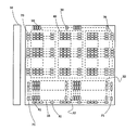
- FIG. 1 is a plan view at the time of ink application in the ink jet method of the first embodiment.
- FIG. 2 is a plan view schematically showing the substrate according to the first embodiment in an enlarged manner, and portions denoted by (a) to (c) correspond to different portions of the substrate, respectively.
- FIG. 3 is a plan view at the time of ink application in the ink jet method of the second embodiment.
- FIG. 4 is a plan view at the time of ink application in the ink jet method of the third embodiment.
- FIG. 5 is a plan view schematically showing the substrate according to the third embodiment in an enlarged manner, and portions with (a) to (c) correspond to different portions of the substrate, respectively.
- FIG. 6 is a view collectively showing (a) a plan view when ink is applied in a conventional ink jet method, and (b) a plan view of a conventional substrate, and a portion marked with (a) is a conventional ink jet. This corresponds to a plan view when ink is applied in the method, and a portion with (b) corresponds to a plan view of a conventional substrate.
- FIG. 7 is a plan view at the time of ink application in a plurality of conventional ink jet methods.
- FIG. 1 shows a plan view of the substrate 12 of the first embodiment.
- Two different sizes of the first panel region 14 and the second panel region 15 (hereinafter may be collectively referred to as “panel region”) are on one substrate 12.
- a first dummy cell 30 and a second dummy cell 31 are provided on the outer periphery of each of the first panel region 14 and the second panel region 15.
- no dummy cell is provided between the panel regions 32.
- the substrate 12 is a glass substrate.
- a single substrate 12 includes a plurality of first panel regions 14 and a second panel region 15, and a plurality of panels are manufactured by cutting out each panel region from the substrate 12.
- an organic EL display panel is assumed.
- the panel is a product such as another display or a device.
- the outer periphery means the peripheral portion of the panel area not including the inside of the panel area.
- the cell is a portion that occupies a part of the panel region, and is a portion that bears one function when it is a final product.
- the panel is an organic EL display panel, and the cell corresponds to a subpixel. In some cases, cells are surrounded by banks or sandwiched between them.
- the shape of the first dummy cell 30 is not the first cell 40 of the first panel region 14 but the same shape as the second cell 41 of the second panel region 15 or a similar shape.
- the shape of the second dummy cell 31 is not the second cell 41 of the second panel region 15 but the same shape as the first cell 40 of the first panel region 14 or a similar shape.
- the direction of the first dummy cell 30 is the same as the direction of the second cell 41 in the second panel region 15, and the direction of the second dummy cell 31 is the same as the direction of the first cell 40 in the first panel region 14. is there.
- the distance between the first dummy cell 30 and the first cell 40 adjacent to the first dummy cell 30 is equal to the first cell 40 adjacent to the second panel region 15 adjacent to the first panel region 14 and the first cell 40. This is the same as the distance from the second cell 41 adjacent to the cell 40.
- the first panel region 14 is outside the first panel region 14 on both sides in a predetermined first direction (the vertical direction in FIG. 1 and the longitudinal direction of the first panel region 14).
- the dummy cell 30 and the second cell 41 are located.
- the first dummy cell 30 and the second cell 41 have the same shape or similar shapes.
- the first dummy cell 30 and the second cell 41 are in an axially symmetric relationship with respect to the axis that virtually passes through the first panel region 14.
- the geometric symmetry of the first panel region 14 including the first dummy cells 30 and the second cells 41 is improved, and the ink applied to each of the first cells 40 in the first panel region 14 is It is dried uniformly and no unevenness occurs.
- the second panel region 15 is located outside the second panel region 15 on both sides in a predetermined first direction (the vertical direction in FIG. 1 and the short direction of the second panel region 15).
- Two dummy cells 31 and a first cell 49 are located.
- the second dummy cell 31 and the first cell 40 have the same shape or similar shapes.
- the second dummy cell 31 and the first cell 40 are in an axially symmetric relationship with respect to a virtual axis that virtually passes through the second panel region 15.
- the geometric symmetry of the second panel region 15 including the second dummy cells 31 and the first cells 40 is improved, and the ink applied to each of the second cells 41 of the second panel region 15 is It is dried uniformly and no unevenness occurs.
- each panel region is often vertical.
- each cell included in each panel region is often rectangular.
- the longitudinal directions of the rectangles of the first dummy cell 30 and the first cell 40 are vertical.
- the longitudinal directions of the rectangles of the second dummy cell 31 and the second cell 41 are also vertical.
- the first dummy cell 30 having the same shape is provided on one side of a predetermined first direction (vertical direction in FIG. 2) outside the first panel region 14;
- the second cell 41 is disposed on the other side.
- the first dummy cell 30 having a shape different from that of the first dummy cell 30 shown in the portion with (a) is shown. That is, one for every two second cells 41 is made one.
- to make one for every two second cells 41 means that the smallest square including two adjacent second cells 41 and the first dummy cell 30 have the same shape.
- FIG. 2 (c) shows a first dummy cell 30 having a shape different from that of the first dummy cell 30 shown in FIG. 2 (a). That is, the shape of the first dummy cell 30 shown in the part marked with (c) is similar to the shape of the second cell 41.
- the first cells 40 disposed at both ends of the first panel region 14 in a predetermined first direction can be dried in a similar environment. Therefore, unevenness due to the cells at the upper and lower ends does not occur. Similar effects can be obtained for the second panel region 15 by providing the second dummy cells 31 similarly to the first panel region 14.
- FIG. 3 corresponds to FIG.
- the difference from the state of the substrate 12 shown in FIG. 1 is that it is outside the first panel region 14 and the second panel region 15, and is in a second direction that intersects (orthogonally) the first direction (FIG. 3).
- the third dummy cell 70 and the fourth dummy cell 71 are also provided on both sides in the horizontal direction.
- the third dummy cell 70 has the same shape as the first cell 40.
- the fourth dummy cell 71 has the same shape as the second cell 41.
- both the first panel region 14 and the second panel region 15 have the same environment when drying in the second direction, and unevenness due to both ends in the second direction of the cells in the panel region does not occur.
- FIG. 4 is a diagram corresponding to FIGS.
- the difference from FIGS. 1 and 3 is that one type of dummy cell is used, and dummy cells are also provided between the panel regions 32.
- the fifth dummy cells 80 are provided on the entire outer periphery of the first panel region 14 and the second panel region 15.
- the shape of the fifth dummy cell 80 is different from the first cell 40 and the second cell 41, and is a combination of them.
- a fifth dummy cell 80 is provided around the first panel region 14.
- the same dummy cells are arranged on the outer periphery corresponding to both ends of the first direction which is the longitudinal direction of the first panel region 14 and the outer periphery corresponding to both ends of the first panel region 14 in the second direction which is the short direction. Therefore, symmetry is good and unevenness does not occur.
- fifth dummy cells 80 are also provided between the panel regions 32.
- the reason for this is that the shape of the fifth dummy cell 80 is different from that of the first cell 40 and the second cell 41, so that more influence is generated in the panel region.
- the shape of the fifth dummy cell 80 will be described with reference to FIG. 5B is a plan view in the case where the first cell 40 and the second cell 41 are virtually overlapped.
- the fifth dummy cell 80 has a shape in which the first cell 40 and the second cell 41 are combined.
- the shape of the fifth dummy cell 80 is a minimum square that can include the first cell 40 and the second cell 41 that are virtually overlapped so that the centers thereof coincide with each other, or a similar shape thereof.
- the first cell 40 and the second cell 41 are each rectangular, the longitudinal direction thereof is vertical, and the lengths in the longitudinal direction are the same. Therefore, the fifth dummy cell 80 is preferably square.
- the reason for making it square is to make it easier to apply ink.
- the outer periphery is used to increase the influence of the first cell 40 and the second cell 41.
- the size of the fifth dummy cell 80 needs to be at least the area of the first cell 40 and the second cell 41 that are virtually overlapped so that their centers coincide.
- the minimum size is indicated by a dotted line in the part marked with (b) in FIG.
- the fifth dummy cell 80 is adjacent to the first cell 40 and the second cell 41 that are virtually overlapped so that the centers thereof coincide with each other, as shown in the part with (c) in FIG.
- positioned may be sufficient.
- both the left and right ends of the first panel region 14 and the second panel region 15 have the same environment, and unevenness due to the left and right end cells does not occur.
- the present invention is not limited to the above embodiment.
- another embodiment realized by arbitrarily combining the components described in this specification and excluding some of the components may be used as an embodiment of the present invention.
- the present invention includes modifications obtained by making various modifications conceivable by those skilled in the art without departing from the gist of the present invention, that is, the meaning of the words described in the claims. It is.
- a rectangular first panel region having a plurality of first cells arranged on a single substrate and a plurality of second cells arranged on the substrate, the size being the same as the first panel region.
- a second dummy cell having the same shape as the plurality of formed first cells.
- a third dummy cell having the same shape as the plurality of first cells formed on the other side of the outer periphery adjacent to the one side of the first panel region; and an outer periphery adjacent to the one side of the second panel region. It is good also as a board
- a substrate without a dummy cell may be provided between the first panel region and the second panel region.
- first cell, the second cell, the first dummy cell, and the second dummy cell are rectangular, and the longitudinal direction of the rectangle of the first cell and the first dummy cell is vertical, and the second cell Further, a substrate in which the longitudinal direction of the rectangle of the second dummy cell is vertical may be used.
- the first panel has a rectangular first panel region having a plurality of rectangular first cells arranged on a single substrate, and a plurality of rectangular second cells arranged on the substrate.
- the substrate may include a square second panel region having a size different from that of the region, an outer periphery of the first panel region, and a square fifth dummy cell provided on the outer periphery of the second panel region.
- first panel region and the first panel region may be a rectangle, and the first panel region and the rectangle of the first panel region may be a substrate whose longitudinal direction is vertical.
- first panel region and the second panel region having different sizes are disposed adjacent to each other on a single substrate, and a second side in the second panel region is disposed on one side of the outer periphery of the first panel region.
- a first dummy cell having the same shape as the cell is formed, and the substrate on which a second dummy cell having the same shape as the first cell in the first panel region is formed on one side of the outer periphery of the second panel region is prepared.
- a panel manufacturing method including a preparation step, an application step of applying ink to the first cell, the second cell, the first dummy cell, and the second dummy cell by an inkjet method, and a drying step of drying the substrate. Good.
- a third dummy cell having the same shape as the first cell is provided on one side of the first panel region that is not adjacent to the second panel region, and one side of the second panel region that is not adjacent to the first panel region.
- a panel manufacturing method may be used in which a fourth dummy cell having the same shape as the second cell is provided.
- first panel region and the second panel region having different sizes are disposed adjacent to each other on a single substrate, and the first panel region and the second panel region are arranged on the respective sides of the outer periphery.
- the manufacturing method may be used.
- the cell of the embodiment in which the vertical direction and the horizontal direction of the substrate 12 are different may be used.
- the method of the present invention can be used when a plurality of devices and displays are produced from a substrate.
Landscapes
- Engineering & Computer Science (AREA)
- Manufacturing & Machinery (AREA)
- Electroluminescent Light Sources (AREA)
- Devices For Indicating Variable Information By Combining Individual Elements (AREA)
Abstract
Description
図1に、実施の形態1の基板12の平面図を示す。2つの異なる大きさの第1パネル領域14と、第2パネル領域15(以下、これらを「パネル領域」と総称する場合がある)とが、1つの基板12上にある。さらに、第1パネル領域14、第2パネル領域15のそれぞれの外周に、第1ダミーセル30、第2ダミーセル31を設けている。しかし、パネル領域間32には、ダミーセルを設けていない。
実施の形態2を、図3を用いて説明する。図3は、図1に相当する図である。図1に示した基板12の状態との違いは、第1パネル領域14、および、第2パネル領域15の外側であって、前記第一方向とは交差(直交)する第二方向(図3中において左右方向)の両側にも、第3ダミーセル70、第4ダミーセル71を設けたものである。
実施の形態3を、図4を用いて説明する。図4は、図1、3に相当する図である。図1、3との違いは、ダミーセルを1種類にしたこと、パネル領域間32にもダミーセルを設けたことである。
なお、本発明は、上記実施の形態に限定されるものではない。例えば、本明細書において記載した構成要素を任意に組み合わせて、また、構成要素のいくつかを除外して実現される別の実施の形態を本発明の実施の形態としてもよい。また、上記実施の形態に対して本発明の主旨、すなわち、請求の範囲に記載される文言が示す意味を逸脱しない範囲で当業者が思いつく各種変形を施して得られる変形例も本発明に含まれる。
本方法によれば、基板上に複数の異なった向きを有するパネル領域にインクジェット塗布にてインクを塗布する際、それぞれのパネル領域の第一方向、第二方向(左右、上下方向)が対称となるようにダミーセルをパターニングすることにより、塗布後の機能層の膜厚分布を第一方向、第二方向(左右、上下)において対称にすることができる。
12 基板
13 セル
14 第1パネル領域
15 第2パネル領域
20 第1ダミーセル
21 第2ダミーセル
30 第1ダミーセル
31 第2ダミーセル
32 パネル領域間
40 第1セル
41 第2セル
70 第3ダミーセル
71 第4ダミーセル
80 第5ダミーセル
Claims (9)
- 1枚の基板上に配置された複数の第1セルを有する方形の第1パネル領域と、
前記基板上に配置された複数の第2セルを有し、前記第1パネル領域と大きさが異なる方形の第2パネル領域と、
前記第1パネル領域に対し前記第1パネル領域に隣接する前記第2パネル領域の反対側の辺に対応する前記第1パネル領域の外周に形成された前記第2セルと同じ形状の第1ダミーセルと、
前記第2パネル領域に対し前記第2パネル領域に隣接する前記第1パネル領域の反対側の辺に対応する前記第2パネル領域の外周に形成された前記第1セルと同じ形状の第2ダミーセルと、
を備える基板。 - 前記第1ダミーセルが形成された辺の隣の辺に対応する前記第1パネル領域の外周に形成され、前記複数の第1セルと同じ形状の第3ダミーセルと、
前記第2ダミーセルが形成された辺の隣の辺に対応する前記第2パネル領域の外周に形成され、前記複数の第2セルと同じ形状の第4ダミーセルと、
を備える請求項1に記載の基板。 - 前記第1パネル領域と前記第2パネル領域との間には、ダミーセルを設けない
請求項1または2に記載の基板。 - 前記第1セル、前記第2セル、前記第1ダミーセル、前記第2ダミーセルは、長方形であり、
前記第1セルの長手方向と前記第1ダミーセルの長手方向とが垂直であり、
前記第2セルの長手方向と前記第2ダミーセルの長手方向とが垂直である
請求項1から3のいずれか1項に記載の基板。 - 1枚の基板上に配置された複数の長方形の第1セルを有する方形の第1パネル領域と、
前記基板上に配置された複数の長方形の第2セルを有し、前記第1パネル領域と大きさが異なる方形の第2パネル領域と、
前記第1パネル領域の外周と、前記第2パネル領域の外周とに設けられた正方形の第5ダミーセルと、
を備える基板。 - 前記第1パネル領域と前記第2パネル領域とは長方形であり、
前記第1パネル領域の長手方向と前記第2パネル領域の長手方向が垂直である
請求項1から5のいずれか1項に記載の基板。 - 1枚の基板上に大きさの異なる第1パネル領域、および、第2パネル領域を配置し、前記第1パネル領域の外周に、前記第2パネル領域内の第2セルと同じ形状の第1ダミーセルを形成し、前記第2パネル領域の外周に、前記第1パネル領域内の第1セルと同じ形状の第2ダミーセルを形成した前記基板を準備する準備工程と、
インクジェット法により、前記第1セル、前記第2セル、前記第1ダミーセル、前記第2ダミーセルにインクを塗布する塗布工程と、
前記基板を乾燥する乾燥工程と、
を含むパネルの製造方法。 - 前記第1パネル領域の前記第2パネル領域と隣接しない外周に、前記第1セルと同じ形状の第3ダミーセルを設け、
前記第2パネル領域の前記第1パネル領域と隣接しない外周に、前記第2セルと同じ形状の第4ダミーセルを設ける
請求項7に記載のパネルの製造方法。 - 1枚の基板上に大きさの異なる第1パネル領域と第2パネル領域とを隣接して配置し、前記第1パネル領域の外周と、前記第2パネル領域の外周のそれぞれに第5ダミーセルを形成した前記基板を準備する準備工程と、
インクジェット法により、前記第1パネル領域内の第1セル、前記第2パネル領域内の第2セル、前記第5ダミーセルにインクを塗布する塗布工程と、
前記基板を乾燥する乾燥工程と、を含むパネルの製造方法であり、
前記第5ダミーセルの形状は、前記第1セルの形状と前記第2セルの形状とを合わせた形状である
パネルの製造方法。
Priority Applications (2)
| Application Number | Priority Date | Filing Date | Title |
|---|---|---|---|
| JP2016523137A JP6268351B2 (ja) | 2014-05-27 | 2015-05-22 | 基板、および、パネルの製造方法 |
| US15/313,044 US20170200772A1 (en) | 2014-05-27 | 2015-05-22 | Substrate and method of manufacturing panel |
Applications Claiming Priority (2)
| Application Number | Priority Date | Filing Date | Title |
|---|---|---|---|
| JP2014-108700 | 2014-05-27 | ||
| JP2014108700 | 2014-05-27 |
Publications (1)
| Publication Number | Publication Date |
|---|---|
| WO2015182098A1 true WO2015182098A1 (ja) | 2015-12-03 |
Family
ID=54698451
Family Applications (1)
| Application Number | Title | Priority Date | Filing Date |
|---|---|---|---|
| PCT/JP2015/002604 Ceased WO2015182098A1 (ja) | 2014-05-27 | 2015-05-22 | 基板、および、パネルの製造方法 |
Country Status (3)
| Country | Link |
|---|---|
| US (1) | US20170200772A1 (ja) |
| JP (1) | JP6268351B2 (ja) |
| WO (1) | WO2015182098A1 (ja) |
Cited By (1)
| Publication number | Priority date | Publication date | Assignee | Title |
|---|---|---|---|---|
| CN117656684A (zh) * | 2022-09-06 | 2024-03-08 | 细美事有限公司 | 多模型印刷方法、计算装置及多模型印刷设备 |
Families Citing this family (3)
| Publication number | Priority date | Publication date | Assignee | Title |
|---|---|---|---|---|
| KR102506430B1 (ko) * | 2015-11-27 | 2023-03-08 | 삼성전자주식회사 | 반도체 장치의 제조 방법 |
| CN110010668B (zh) * | 2019-04-09 | 2021-07-27 | 武汉天马微电子有限公司 | 有机发光显示面板和显示装置 |
| CN111430419A (zh) * | 2020-04-01 | 2020-07-17 | 深圳市华星光电半导体显示技术有限公司 | 一种横置像素结构、混合排列面板及制程方法 |
Citations (5)
| Publication number | Priority date | Publication date | Assignee | Title |
|---|---|---|---|---|
| JP2002222695A (ja) * | 2000-11-27 | 2002-08-09 | Seiko Epson Corp | 有機エレクトロルミネッセンス装置の製造方法および有機エレクトロルミネッセンス装置並びに電子機器 |
| JP2005235769A (ja) * | 2004-02-19 | 2005-09-02 | Samsung Electronics Co Ltd | 表示装置、これの製造方法及び有機物滴下装置 |
| JP2007080603A (ja) * | 2005-09-13 | 2007-03-29 | Seiko Epson Corp | 膜パターンの形成方法、デバイスの製造方法、有機エレクトロルミネッセンス装置 |
| JP2010073602A (ja) * | 2008-09-22 | 2010-04-02 | Seiko Epson Corp | 有機el装置の製造方法 |
| WO2011001614A1 (ja) * | 2009-06-29 | 2011-01-06 | パナソニック株式会社 | 有機elディスプレイパネル |
Family Cites Families (3)
| Publication number | Priority date | Publication date | Assignee | Title |
|---|---|---|---|---|
| JP2004362818A (ja) * | 2003-06-02 | 2004-12-24 | Seiko Epson Corp | 薄膜パターンの製造方法、有機電界発光素子の製造方法、カラーフィルタの製造方法、プラズマディスプレイパネルの製造方法、液晶表示パネルの製造方法及び電子機器 |
| JP2010277944A (ja) * | 2009-06-01 | 2010-12-09 | Panasonic Corp | 有機elディスプレイパネルおよびその製造方法 |
| KR102050383B1 (ko) * | 2012-12-28 | 2019-11-29 | 엘지디스플레이 주식회사 | 유기전계발광표시장치 |
-
2015
- 2015-05-22 WO PCT/JP2015/002604 patent/WO2015182098A1/ja not_active Ceased
- 2015-05-22 US US15/313,044 patent/US20170200772A1/en not_active Abandoned
- 2015-05-22 JP JP2016523137A patent/JP6268351B2/ja active Active
Patent Citations (5)
| Publication number | Priority date | Publication date | Assignee | Title |
|---|---|---|---|---|
| JP2002222695A (ja) * | 2000-11-27 | 2002-08-09 | Seiko Epson Corp | 有機エレクトロルミネッセンス装置の製造方法および有機エレクトロルミネッセンス装置並びに電子機器 |
| JP2005235769A (ja) * | 2004-02-19 | 2005-09-02 | Samsung Electronics Co Ltd | 表示装置、これの製造方法及び有機物滴下装置 |
| JP2007080603A (ja) * | 2005-09-13 | 2007-03-29 | Seiko Epson Corp | 膜パターンの形成方法、デバイスの製造方法、有機エレクトロルミネッセンス装置 |
| JP2010073602A (ja) * | 2008-09-22 | 2010-04-02 | Seiko Epson Corp | 有機el装置の製造方法 |
| WO2011001614A1 (ja) * | 2009-06-29 | 2011-01-06 | パナソニック株式会社 | 有機elディスプレイパネル |
Cited By (3)
| Publication number | Priority date | Publication date | Assignee | Title |
|---|---|---|---|---|
| CN117656684A (zh) * | 2022-09-06 | 2024-03-08 | 细美事有限公司 | 多模型印刷方法、计算装置及多模型印刷设备 |
| US12118251B2 (en) | 2022-09-06 | 2024-10-15 | Semes Co., Ltd. | Multi-model printing method, computing device and multi-model printing apparatus |
| JP7569366B2 (ja) | 2022-09-06 | 2024-10-17 | セメス株式会社 | マルチモデルプリンティング方法 |
Also Published As
| Publication number | Publication date |
|---|---|
| JPWO2015182098A1 (ja) | 2017-04-20 |
| JP6268351B2 (ja) | 2018-01-31 |
| US20170200772A1 (en) | 2017-07-13 |
Similar Documents
| Publication | Publication Date | Title |
|---|---|---|
| US10446622B2 (en) | OLED pixel defining structure with at least two intercommunicated sub-pixel defining zones of same color, manufacturing method thereof and array substrate | |
| CN109585490B (zh) | 像素界定层、喷墨打印方法、显示基板及其制造方法、显示装置 | |
| US9583708B2 (en) | Mask for deposition, mask assembly including the same and method of forming the mask assembly | |
| US9647039B1 (en) | Array substrate, display panel, display device, and fabrication method thereof | |
| CN108281476B (zh) | 像素界定层和显示面板及其制作方法、显示装置 | |
| KR102862449B1 (ko) | 전계 발광 표시 장치 | |
| US20150001512A1 (en) | Pixel structure and mask for manufacturing the same | |
| CN108598141B (zh) | 一种像素显示模组以及制作像素显示模组的掩膜板 | |
| TW201635258A (zh) | 畫素結構 | |
| WO2016050012A1 (zh) | 阵列基板、掩膜板和显示装置 | |
| KR102028989B1 (ko) | Oled 표시 장치 | |
| JP6268351B2 (ja) | 基板、および、パネルの製造方法 | |
| US10020356B2 (en) | Organic light-emitting diode display device | |
| KR20160067544A (ko) | 유기전계 발광소자 및 이의 제조방법 | |
| WO2021227153A1 (zh) | 显示面板 | |
| CN105140421A (zh) | 掩膜板组及制作电致发光层的方法、显示面板及驱动方法 | |
| TW201507130A (zh) | 有機發光二極體顯示面板 | |
| CN107742637A (zh) | 一种像素结构、掩膜版、显示面板及显示装置 | |
| KR20140119253A (ko) | Oled 표시 장치 및 그의 제조 방법 | |
| US9269752B2 (en) | Organic electroluminescence display | |
| CN104617129A (zh) | 一种显示面板、掩模板和显示装置 | |
| CN106298833B (zh) | 像素结构 | |
| CN204270613U (zh) | 一种像素结构、显示基板及显示装置 | |
| CN104464539B (zh) | 一种像素结构、显示基板及显示装置 | |
| CN104637972A (zh) | 一种高分辨率的有机发光显示器及其制造方法 |
Legal Events
| Date | Code | Title | Description |
|---|---|---|---|
| 121 | Ep: the epo has been informed by wipo that ep was designated in this application |
Ref document number: 15799157 Country of ref document: EP Kind code of ref document: A1 |
|
| WWE | Wipo information: entry into national phase |
Ref document number: 15313044 Country of ref document: US |
|
| ENP | Entry into the national phase |
Ref document number: 2016523137 Country of ref document: JP Kind code of ref document: A |
|
| NENP | Non-entry into the national phase |
Ref country code: DE |
|
| 122 | Ep: pct application non-entry in european phase |
Ref document number: 15799157 Country of ref document: EP Kind code of ref document: A1 |