WO2015182001A1 - Module électroluminescent organique, dispositif intelligent et dispositif d'éclairage - Google Patents
Module électroluminescent organique, dispositif intelligent et dispositif d'éclairage Download PDFInfo
- Publication number
- WO2015182001A1 WO2015182001A1 PCT/JP2014/074697 JP2014074697W WO2015182001A1 WO 2015182001 A1 WO2015182001 A1 WO 2015182001A1 JP 2014074697 W JP2014074697 W JP 2014074697W WO 2015182001 A1 WO2015182001 A1 WO 2015182001A1
- Authority
- WO
- WIPO (PCT)
- Prior art keywords
- circuit unit
- organic electroluminescence
- touch detection
- organic
- light emitting
- Prior art date
Links
- 238000005401 electroluminescence Methods 0.000 title claims description 99
- 238000001514 detection method Methods 0.000 claims abstract description 165
- 238000000034 method Methods 0.000 claims description 62
- 238000007667 floating Methods 0.000 claims description 16
- 230000002441 reversible effect Effects 0.000 claims description 15
- 239000003990 capacitor Substances 0.000 claims description 14
- 238000005286 illumination Methods 0.000 claims 1
- 238000004519 manufacturing process Methods 0.000 abstract description 5
- 230000009467 reduction Effects 0.000 abstract description 3
- 239000010410 layer Substances 0.000 description 192
- 239000000463 material Substances 0.000 description 47
- 150000001875 compounds Chemical class 0.000 description 43
- 238000002347 injection Methods 0.000 description 35
- 239000007924 injection Substances 0.000 description 35
- 238000010586 diagram Methods 0.000 description 31
- 230000000903 blocking effect Effects 0.000 description 25
- -1 polyethylene terephthalate Polymers 0.000 description 25
- 230000005525 hole transport Effects 0.000 description 24
- 229910052709 silver Inorganic materials 0.000 description 24
- BQCADISMDOOEFD-UHFFFAOYSA-N Silver Chemical compound [Ag] BQCADISMDOOEFD-UHFFFAOYSA-N 0.000 description 23
- 239000004332 silver Substances 0.000 description 23
- 239000002346 layers by function Substances 0.000 description 22
- 229910052751 metal Inorganic materials 0.000 description 21
- 239000002184 metal Substances 0.000 description 21
- 239000000758 substrate Substances 0.000 description 18
- 238000007789 sealing Methods 0.000 description 16
- 229910052757 nitrogen Inorganic materials 0.000 description 15
- 239000010408 film Substances 0.000 description 14
- 239000000975 dye Substances 0.000 description 12
- 239000011521 glass Substances 0.000 description 11
- KDLHZDBZIXYQEI-UHFFFAOYSA-N Palladium Chemical compound [Pd] KDLHZDBZIXYQEI-UHFFFAOYSA-N 0.000 description 10
- 239000011347 resin Substances 0.000 description 10
- 229920005989 resin Polymers 0.000 description 10
- 239000010949 copper Substances 0.000 description 9
- 239000011777 magnesium Substances 0.000 description 9
- 239000010409 thin film Substances 0.000 description 9
- 229910052749 magnesium Inorganic materials 0.000 description 8
- FYYHWMGAXLPEAU-UHFFFAOYSA-N Magnesium Chemical compound [Mg] FYYHWMGAXLPEAU-UHFFFAOYSA-N 0.000 description 7
- 239000000956 alloy Substances 0.000 description 7
- 229910045601 alloy Inorganic materials 0.000 description 7
- 239000002585 base Substances 0.000 description 7
- 229910052802 copper Inorganic materials 0.000 description 7
- 239000000203 mixture Substances 0.000 description 7
- 238000006862 quantum yield reaction Methods 0.000 description 7
- RYGMFSIKBFXOCR-UHFFFAOYSA-N Copper Chemical compound [Cu] RYGMFSIKBFXOCR-UHFFFAOYSA-N 0.000 description 6
- PXHVJJICTQNCMI-UHFFFAOYSA-N Nickel Chemical compound [Ni] PXHVJJICTQNCMI-UHFFFAOYSA-N 0.000 description 6
- 239000010931 gold Substances 0.000 description 6
- 239000002245 particle Substances 0.000 description 6
- VYPSYNLAJGMNEJ-UHFFFAOYSA-N silicon dioxide Inorganic materials O=[Si]=O VYPSYNLAJGMNEJ-UHFFFAOYSA-N 0.000 description 6
- 229910052782 aluminium Inorganic materials 0.000 description 5
- XAGFODPZIPBFFR-UHFFFAOYSA-N aluminium Chemical compound [Al] XAGFODPZIPBFFR-UHFFFAOYSA-N 0.000 description 5
- MWPLVEDNUUSJAV-UHFFFAOYSA-N anthracene Chemical class C1=CC=CC2=CC3=CC=CC=C3C=C21 MWPLVEDNUUSJAV-UHFFFAOYSA-N 0.000 description 5
- 239000000470 constituent Substances 0.000 description 5
- 239000006059 cover glass Substances 0.000 description 5
- 239000007850 fluorescent dye Substances 0.000 description 5
- 239000007789 gas Substances 0.000 description 5
- 229910052737 gold Inorganic materials 0.000 description 5
- 239000004973 liquid crystal related substance Substances 0.000 description 5
- 230000003287 optical effect Effects 0.000 description 5
- 230000008569 process Effects 0.000 description 5
- 238000004528 spin coating Methods 0.000 description 5
- 238000007740 vapor deposition Methods 0.000 description 5
- 230000004888 barrier function Effects 0.000 description 4
- 238000005266 casting Methods 0.000 description 4
- 150000004696 coordination complex Chemical class 0.000 description 4
- 239000007772 electrode material Substances 0.000 description 4
- PCHJSUWPFVWCPO-UHFFFAOYSA-N gold Chemical compound [Au] PCHJSUWPFVWCPO-UHFFFAOYSA-N 0.000 description 4
- 150000004866 oxadiazoles Chemical class 0.000 description 4
- 239000001301 oxygen Substances 0.000 description 4
- 229910052760 oxygen Inorganic materials 0.000 description 4
- 229910052763 palladium Inorganic materials 0.000 description 4
- 229920000642 polymer Polymers 0.000 description 4
- 238000007639 printing Methods 0.000 description 4
- 239000012945 sealing adhesive Substances 0.000 description 4
- 239000002356 single layer Substances 0.000 description 4
- PJANXHGTPQOBST-UHFFFAOYSA-N stilbene Chemical compound C=1C=CC=CC=1C=CC1=CC=CC=C1 PJANXHGTPQOBST-UHFFFAOYSA-N 0.000 description 4
- 238000001771 vacuum deposition Methods 0.000 description 4
- QVGXLLKOCUKJST-UHFFFAOYSA-N atomic oxygen Chemical compound [O] QVGXLLKOCUKJST-UHFFFAOYSA-N 0.000 description 3
- 239000005388 borosilicate glass Substances 0.000 description 3
- 230000000052 comparative effect Effects 0.000 description 3
- 238000007599 discharging Methods 0.000 description 3
- 239000002019 doping agent Substances 0.000 description 3
- 229910052738 indium Inorganic materials 0.000 description 3
- 150000002504 iridium compounds Chemical class 0.000 description 3
- 150000002739 metals Chemical class 0.000 description 3
- 229910052759 nickel Inorganic materials 0.000 description 3
- IJGRMHOSHXDMSA-UHFFFAOYSA-N nitrogen Substances N#N IJGRMHOSHXDMSA-UHFFFAOYSA-N 0.000 description 3
- 229920000139 polyethylene terephthalate Polymers 0.000 description 3
- 239000005020 polyethylene terephthalate Substances 0.000 description 3
- 229910052761 rare earth metal Inorganic materials 0.000 description 3
- 150000002910 rare earth metals Chemical class 0.000 description 3
- 235000012239 silicon dioxide Nutrition 0.000 description 3
- 238000004544 sputter deposition Methods 0.000 description 3
- 229910052717 sulfur Inorganic materials 0.000 description 3
- 238000002834 transmittance Methods 0.000 description 3
- 125000005259 triarylamine group Chemical group 0.000 description 3
- UWRZIZXBOLBCON-VOTSOKGWSA-N (e)-2-phenylethenamine Chemical class N\C=C\C1=CC=CC=C1 UWRZIZXBOLBCON-VOTSOKGWSA-N 0.000 description 2
- XKRFYHLGVUSROY-UHFFFAOYSA-N Argon Chemical compound [Ar] XKRFYHLGVUSROY-UHFFFAOYSA-N 0.000 description 2
- XEEYBQQBJWHFJM-UHFFFAOYSA-N Iron Chemical compound [Fe] XEEYBQQBJWHFJM-UHFFFAOYSA-N 0.000 description 2
- WHXSMMKQMYFTQS-UHFFFAOYSA-N Lithium Chemical compound [Li] WHXSMMKQMYFTQS-UHFFFAOYSA-N 0.000 description 2
- PAYRUJLWNCNPSJ-UHFFFAOYSA-N N-phenyl amine Natural products NC1=CC=CC=C1 PAYRUJLWNCNPSJ-UHFFFAOYSA-N 0.000 description 2
- UFWIBTONFRDIAS-UHFFFAOYSA-N Naphthalene Chemical compound C1=CC=CC2=CC=CC=C21 UFWIBTONFRDIAS-UHFFFAOYSA-N 0.000 description 2
- 229920001609 Poly(3,4-ethylenedioxythiophene) Polymers 0.000 description 2
- 239000004698 Polyethylene Substances 0.000 description 2
- XUIMIQQOPSSXEZ-UHFFFAOYSA-N Silicon Chemical compound [Si] XUIMIQQOPSSXEZ-UHFFFAOYSA-N 0.000 description 2
- 229910006404 SnO 2 Inorganic materials 0.000 description 2
- PJANXHGTPQOBST-VAWYXSNFSA-N Stilbene Natural products C=1C=CC=CC=1/C=C/C1=CC=CC=C1 PJANXHGTPQOBST-VAWYXSNFSA-N 0.000 description 2
- YTPLMLYBLZKORZ-UHFFFAOYSA-N Thiophene Chemical compound C=1C=CSC=1 YTPLMLYBLZKORZ-UHFFFAOYSA-N 0.000 description 2
- NIXOWILDQLNWCW-UHFFFAOYSA-N acrylic acid group Chemical group C(C=C)(=O)O NIXOWILDQLNWCW-UHFFFAOYSA-N 0.000 description 2
- 239000000853 adhesive Substances 0.000 description 2
- 230000001070 adhesive effect Effects 0.000 description 2
- 150000004982 aromatic amines Chemical class 0.000 description 2
- 238000005311 autocorrelation function Methods 0.000 description 2
- 229910052788 barium Inorganic materials 0.000 description 2
- DSAJWYNOEDNPEQ-UHFFFAOYSA-N barium atom Chemical compound [Ba] DSAJWYNOEDNPEQ-UHFFFAOYSA-N 0.000 description 2
- 230000015572 biosynthetic process Effects 0.000 description 2
- 239000002131 composite material Substances 0.000 description 2
- 229920001940 conductive polymer Polymers 0.000 description 2
- 229920001577 copolymer Polymers 0.000 description 2
- ZYGHJZDHTFUPRJ-UHFFFAOYSA-N coumarin Chemical compound C1=CC=C2OC(=O)C=CC2=C1 ZYGHJZDHTFUPRJ-UHFFFAOYSA-N 0.000 description 2
- 238000013461 design Methods 0.000 description 2
- 230000000694 effects Effects 0.000 description 2
- NIHNNTQXNPWCJQ-UHFFFAOYSA-N fluorene Chemical compound C1=CC=C2CC3=CC=CC=C3C2=C1 NIHNNTQXNPWCJQ-UHFFFAOYSA-N 0.000 description 2
- 150000008376 fluorenones Chemical class 0.000 description 2
- 239000011888 foil Substances 0.000 description 2
- 229940083761 high-ceiling diuretics pyrazolone derivative Drugs 0.000 description 2
- 150000007857 hydrazones Chemical class 0.000 description 2
- 150000002460 imidazoles Chemical class 0.000 description 2
- APFVFJFRJDLVQX-UHFFFAOYSA-N indium atom Chemical compound [In] APFVFJFRJDLVQX-UHFFFAOYSA-N 0.000 description 2
- 229940079865 intestinal antiinfectives imidazole derivative Drugs 0.000 description 2
- 239000005355 lead glass Substances 0.000 description 2
- 229910052744 lithium Inorganic materials 0.000 description 2
- PQXKHYXIUOZZFA-UHFFFAOYSA-M lithium fluoride Chemical compound [Li+].[F-] PQXKHYXIUOZZFA-UHFFFAOYSA-M 0.000 description 2
- 238000004020 luminiscence type Methods 0.000 description 2
- ORUIBWPALBXDOA-UHFFFAOYSA-L magnesium fluoride Chemical compound [F-].[F-].[Mg+2] ORUIBWPALBXDOA-UHFFFAOYSA-L 0.000 description 2
- 229910001635 magnesium fluoride Inorganic materials 0.000 description 2
- 229910044991 metal oxide Inorganic materials 0.000 description 2
- 150000004706 metal oxides Chemical class 0.000 description 2
- 239000002923 metal particle Substances 0.000 description 2
- IBHBKWKFFTZAHE-UHFFFAOYSA-N n-[4-[4-(n-naphthalen-1-ylanilino)phenyl]phenyl]-n-phenylnaphthalen-1-amine Chemical compound C1=CC=CC=C1N(C=1C2=CC=CC=C2C=CC=1)C1=CC=C(C=2C=CC(=CC=2)N(C=2C=CC=CC=2)C=2C3=CC=CC=C3C=CC=2)C=C1 IBHBKWKFFTZAHE-UHFFFAOYSA-N 0.000 description 2
- 239000012044 organic layer Substances 0.000 description 2
- 239000011368 organic material Substances 0.000 description 2
- 125000002524 organometallic group Chemical group 0.000 description 2
- 150000007978 oxazole derivatives Chemical class 0.000 description 2
- 230000002093 peripheral effect Effects 0.000 description 2
- 230000035699 permeability Effects 0.000 description 2
- 150000004986 phenylenediamines Chemical class 0.000 description 2
- BASFCYQUMIYNBI-UHFFFAOYSA-N platinum Chemical compound [Pt] BASFCYQUMIYNBI-UHFFFAOYSA-N 0.000 description 2
- 229920000172 poly(styrenesulfonic acid) Polymers 0.000 description 2
- 239000004417 polycarbonate Substances 0.000 description 2
- 229920000515 polycarbonate Polymers 0.000 description 2
- 229920000573 polyethylene Polymers 0.000 description 2
- 229920006254 polymer film Polymers 0.000 description 2
- 239000002861 polymer material Substances 0.000 description 2
- 229940005642 polystyrene sulfonic acid Drugs 0.000 description 2
- 229920000123 polythiophene Polymers 0.000 description 2
- NROKBHXJSPEDAR-UHFFFAOYSA-M potassium fluoride Chemical compound [F-].[K+] NROKBHXJSPEDAR-UHFFFAOYSA-M 0.000 description 2
- JEXVQSWXXUJEMA-UHFFFAOYSA-N pyrazol-3-one Chemical class O=C1C=CN=N1 JEXVQSWXXUJEMA-UHFFFAOYSA-N 0.000 description 2
- 150000003219 pyrazolines Chemical class 0.000 description 2
- 239000010453 quartz Substances 0.000 description 2
- 125000001567 quinoxalinyl group Chemical class N1=C(C=NC2=CC=CC=C12)* 0.000 description 2
- 230000006798 recombination Effects 0.000 description 2
- 238000005215 recombination Methods 0.000 description 2
- 239000003566 sealing material Substances 0.000 description 2
- 229910052710 silicon Inorganic materials 0.000 description 2
- 239000010703 silicon Substances 0.000 description 2
- 239000005361 soda-lime glass Substances 0.000 description 2
- PUZPDOWCWNUUKD-UHFFFAOYSA-M sodium fluoride Chemical compound [F-].[Na+] PUZPDOWCWNUUKD-UHFFFAOYSA-M 0.000 description 2
- 239000000243 solution Substances 0.000 description 2
- 239000002904 solvent Substances 0.000 description 2
- 235000021286 stilbenes Nutrition 0.000 description 2
- 229910052712 strontium Inorganic materials 0.000 description 2
- CIOAGBVUUVVLOB-UHFFFAOYSA-N strontium atom Chemical compound [Sr] CIOAGBVUUVVLOB-UHFFFAOYSA-N 0.000 description 2
- 239000000126 substance Substances 0.000 description 2
- 125000004434 sulfur atom Chemical group 0.000 description 2
- 229940042055 systemic antimycotics triazole derivative Drugs 0.000 description 2
- XLYOFNOQVPJJNP-UHFFFAOYSA-N water Chemical compound O XLYOFNOQVPJJNP-UHFFFAOYSA-N 0.000 description 2
- QGKMIGUHVLGJBR-UHFFFAOYSA-M (4z)-1-(3-methylbutyl)-4-[[1-(3-methylbutyl)quinolin-1-ium-4-yl]methylidene]quinoline;iodide Chemical compound [I-].C12=CC=CC=C2N(CCC(C)C)C=CC1=CC1=CC=[N+](CCC(C)C)C2=CC=CC=C12 QGKMIGUHVLGJBR-UHFFFAOYSA-M 0.000 description 1
- VERMWGQSKPXSPZ-BUHFOSPRSA-N 1-[(e)-2-phenylethenyl]anthracene Chemical class C=1C=CC2=CC3=CC=CC=C3C=C2C=1\C=C\C1=CC=CC=C1 VERMWGQSKPXSPZ-BUHFOSPRSA-N 0.000 description 1
- MVWPVABZQQJTPL-UHFFFAOYSA-N 2,3-diphenylcyclohexa-2,5-diene-1,4-dione Chemical class O=C1C=CC(=O)C(C=2C=CC=CC=2)=C1C1=CC=CC=C1 MVWPVABZQQJTPL-UHFFFAOYSA-N 0.000 description 1
- HONWGFNQCPRRFM-UHFFFAOYSA-N 2-n-(3-methylphenyl)-1-n,1-n,2-n-triphenylbenzene-1,2-diamine Chemical compound CC1=CC=CC(N(C=2C=CC=CC=2)C=2C(=CC=CC=2)N(C=2C=CC=CC=2)C=2C=CC=CC=2)=C1 HONWGFNQCPRRFM-UHFFFAOYSA-N 0.000 description 1
- MGADZUXDNSDTHW-UHFFFAOYSA-N 2H-pyran Chemical compound C1OC=CC=C1 MGADZUXDNSDTHW-UHFFFAOYSA-N 0.000 description 1
- DMEVMYSQZPJFOK-UHFFFAOYSA-N 3,4,5,6,9,10-hexazatetracyclo[12.4.0.02,7.08,13]octadeca-1(18),2(7),3,5,8(13),9,11,14,16-nonaene Chemical group N1=NN=C2C3=CC=CC=C3C3=CC=NN=C3C2=N1 DMEVMYSQZPJFOK-UHFFFAOYSA-N 0.000 description 1
- OGGKVJMNFFSDEV-UHFFFAOYSA-N 3-methyl-n-[4-[4-(n-(3-methylphenyl)anilino)phenyl]phenyl]-n-phenylaniline Chemical compound CC1=CC=CC(N(C=2C=CC=CC=2)C=2C=CC(=CC=2)C=2C=CC(=CC=2)N(C=2C=CC=CC=2)C=2C=C(C)C=CC=2)=C1 OGGKVJMNFFSDEV-UHFFFAOYSA-N 0.000 description 1
- PWFFDTZNRAEFIY-UHFFFAOYSA-N 4-(4-aminophenyl)-3-(4-methoxyphenyl)aniline Chemical group C1=CC(OC)=CC=C1C1=CC(N)=CC=C1C1=CC=C(N)C=C1 PWFFDTZNRAEFIY-UHFFFAOYSA-N 0.000 description 1
- AHDTYXOIJHCGKH-UHFFFAOYSA-N 4-[[4-(dimethylamino)-2-methylphenyl]-phenylmethyl]-n,n,3-trimethylaniline Chemical compound CC1=CC(N(C)C)=CC=C1C(C=1C(=CC(=CC=1)N(C)C)C)C1=CC=CC=C1 AHDTYXOIJHCGKH-UHFFFAOYSA-N 0.000 description 1
- MEIBOBDKQKIBJH-UHFFFAOYSA-N 4-methyl-n-[4-[1-[4-(4-methyl-n-(4-methylphenyl)anilino)phenyl]-4-phenylcyclohexyl]phenyl]-n-(4-methylphenyl)aniline Chemical compound C1=CC(C)=CC=C1N(C=1C=CC(=CC=1)C1(CCC(CC1)C=1C=CC=CC=1)C=1C=CC(=CC=1)N(C=1C=CC(C)=CC=1)C=1C=CC(C)=CC=1)C1=CC=C(C)C=C1 MEIBOBDKQKIBJH-UHFFFAOYSA-N 0.000 description 1
- ZOKIJILZFXPFTO-UHFFFAOYSA-N 4-methyl-n-[4-[1-[4-(4-methyl-n-(4-methylphenyl)anilino)phenyl]cyclohexyl]phenyl]-n-(4-methylphenyl)aniline Chemical compound C1=CC(C)=CC=C1N(C=1C=CC(=CC=1)C1(CCCCC1)C=1C=CC(=CC=1)N(C=1C=CC(C)=CC=1)C=1C=CC(C)=CC=1)C1=CC=C(C)C=C1 ZOKIJILZFXPFTO-UHFFFAOYSA-N 0.000 description 1
- DUSWRTUHJVJVRY-UHFFFAOYSA-N 4-methyl-n-[4-[2-[4-(4-methyl-n-(4-methylphenyl)anilino)phenyl]propan-2-yl]phenyl]-n-(4-methylphenyl)aniline Chemical compound C1=CC(C)=CC=C1N(C=1C=CC(=CC=1)C(C)(C)C=1C=CC(=CC=1)N(C=1C=CC(C)=CC=1)C=1C=CC(C)=CC=1)C1=CC=C(C)C=C1 DUSWRTUHJVJVRY-UHFFFAOYSA-N 0.000 description 1
- MVIXNQZIMMIGEL-UHFFFAOYSA-N 4-methyl-n-[4-[4-(4-methyl-n-(4-methylphenyl)anilino)phenyl]phenyl]-n-(4-methylphenyl)aniline Chemical group C1=CC(C)=CC=C1N(C=1C=CC(=CC=1)C=1C=CC(=CC=1)N(C=1C=CC(C)=CC=1)C=1C=CC(C)=CC=1)C1=CC=C(C)C=C1 MVIXNQZIMMIGEL-UHFFFAOYSA-N 0.000 description 1
- XIQGFRHAIQHZBD-UHFFFAOYSA-N 4-methyl-n-[4-[[4-(4-methyl-n-(4-methylphenyl)anilino)phenyl]-phenylmethyl]phenyl]-n-(4-methylphenyl)aniline Chemical compound C1=CC(C)=CC=C1N(C=1C=CC(=CC=1)C(C=1C=CC=CC=1)C=1C=CC(=CC=1)N(C=1C=CC(C)=CC=1)C=1C=CC(C)=CC=1)C1=CC=C(C)C=C1 XIQGFRHAIQHZBD-UHFFFAOYSA-N 0.000 description 1
- ZYASLTYCYTYKFC-UHFFFAOYSA-N 9-methylidenefluorene Chemical class C1=CC=C2C(=C)C3=CC=CC=C3C2=C1 ZYASLTYCYTYKFC-UHFFFAOYSA-N 0.000 description 1
- VIJYEGDOKCKUOL-UHFFFAOYSA-N 9-phenylcarbazole Chemical compound C1=CC=CC=C1N1C2=CC=CC=C2C2=CC=CC=C21 VIJYEGDOKCKUOL-UHFFFAOYSA-N 0.000 description 1
- 238000006677 Appel reaction Methods 0.000 description 1
- 229920000298 Cellophane Polymers 0.000 description 1
- 229920000623 Cellulose acetate phthalate Polymers 0.000 description 1
- 229920001747 Cellulose diacetate Polymers 0.000 description 1
- 229920002284 Cellulose triacetate Polymers 0.000 description 1
- VYZAMTAEIAYCRO-UHFFFAOYSA-N Chromium Chemical compound [Cr] VYZAMTAEIAYCRO-UHFFFAOYSA-N 0.000 description 1
- 241000284156 Clerodendrum quadriloculare Species 0.000 description 1
- IMROMDMJAWUWLK-UHFFFAOYSA-N Ethenol Chemical compound OC=C IMROMDMJAWUWLK-UHFFFAOYSA-N 0.000 description 1
- ZOKXTWBITQBERF-UHFFFAOYSA-N Molybdenum Chemical compound [Mo] ZOKXTWBITQBERF-UHFFFAOYSA-N 0.000 description 1
- 239000000020 Nitrocellulose Substances 0.000 description 1
- 239000004677 Nylon Substances 0.000 description 1
- 229920012266 Poly(ether sulfone) PES Polymers 0.000 description 1
- 239000004952 Polyamide Substances 0.000 description 1
- 239000004697 Polyetherimide Substances 0.000 description 1
- 239000004642 Polyimide Substances 0.000 description 1
- 239000004721 Polyphenylene oxide Substances 0.000 description 1
- 239000004734 Polyphenylene sulfide Substances 0.000 description 1
- 239000004743 Polypropylene Substances 0.000 description 1
- 239000004372 Polyvinyl alcohol Substances 0.000 description 1
- 229920001328 Polyvinylidene chloride Polymers 0.000 description 1
- XBDQKXXYIPTUBI-UHFFFAOYSA-M Propionate Chemical compound CCC([O-])=O XBDQKXXYIPTUBI-UHFFFAOYSA-M 0.000 description 1
- 229910052581 Si3N4 Inorganic materials 0.000 description 1
- UCKMPCXJQFINFW-UHFFFAOYSA-N Sulphide Chemical compound [S-2] UCKMPCXJQFINFW-UHFFFAOYSA-N 0.000 description 1
- 229920010524 Syndiotactic polystyrene Polymers 0.000 description 1
- RTAQQCXQSZGOHL-UHFFFAOYSA-N Titanium Chemical compound [Ti] RTAQQCXQSZGOHL-UHFFFAOYSA-N 0.000 description 1
- 239000007983 Tris buffer Substances 0.000 description 1
- HCHKCACWOHOZIP-UHFFFAOYSA-N Zinc Chemical compound [Zn] HCHKCACWOHOZIP-UHFFFAOYSA-N 0.000 description 1
- NNLVGZFZQQXQNW-ADJNRHBOSA-N [(2r,3r,4s,5r,6s)-4,5-diacetyloxy-3-[(2s,3r,4s,5r,6r)-3,4,5-triacetyloxy-6-(acetyloxymethyl)oxan-2-yl]oxy-6-[(2r,3r,4s,5r,6s)-4,5,6-triacetyloxy-2-(acetyloxymethyl)oxan-3-yl]oxyoxan-2-yl]methyl acetate Chemical compound O([C@@H]1O[C@@H]([C@H]([C@H](OC(C)=O)[C@H]1OC(C)=O)O[C@H]1[C@@H]([C@@H](OC(C)=O)[C@H](OC(C)=O)[C@@H](COC(C)=O)O1)OC(C)=O)COC(=O)C)[C@@H]1[C@@H](COC(C)=O)O[C@@H](OC(C)=O)[C@H](OC(C)=O)[C@H]1OC(C)=O NNLVGZFZQQXQNW-ADJNRHBOSA-N 0.000 description 1
- FJWGYAHXMCUOOM-QHOUIDNNSA-N [(2s,3r,4s,5r,6r)-2-[(2r,3r,4s,5r,6s)-4,5-dinitrooxy-2-(nitrooxymethyl)-6-[(2r,3r,4s,5r,6s)-4,5,6-trinitrooxy-2-(nitrooxymethyl)oxan-3-yl]oxyoxan-3-yl]oxy-3,5-dinitrooxy-6-(nitrooxymethyl)oxan-4-yl] nitrate Chemical compound O([C@@H]1O[C@@H]([C@H]([C@H](O[N+]([O-])=O)[C@H]1O[N+]([O-])=O)O[C@H]1[C@@H]([C@@H](O[N+]([O-])=O)[C@H](O[N+]([O-])=O)[C@@H](CO[N+]([O-])=O)O1)O[N+]([O-])=O)CO[N+](=O)[O-])[C@@H]1[C@@H](CO[N+]([O-])=O)O[C@@H](O[N+]([O-])=O)[C@H](O[N+]([O-])=O)[C@H]1O[N+]([O-])=O FJWGYAHXMCUOOM-QHOUIDNNSA-N 0.000 description 1
- 238000010521 absorption reaction Methods 0.000 description 1
- 239000012790 adhesive layer Substances 0.000 description 1
- 230000002411 adverse Effects 0.000 description 1
- 150000001339 alkali metal compounds Chemical class 0.000 description 1
- 229910001508 alkali metal halide Inorganic materials 0.000 description 1
- 150000008045 alkali metal halides Chemical class 0.000 description 1
- 150000001341 alkaline earth metal compounds Chemical class 0.000 description 1
- 239000005354 aluminosilicate glass Substances 0.000 description 1
- 239000010405 anode material Substances 0.000 description 1
- 150000008425 anthrones Chemical class 0.000 description 1
- 229940045985 antineoplastic platinum compound Drugs 0.000 description 1
- 229910052786 argon Inorganic materials 0.000 description 1
- HFACYLZERDEVSX-UHFFFAOYSA-N benzidine Chemical compound C1=CC(N)=CC=C1C1=CC=C(N)C=C1 HFACYLZERDEVSX-UHFFFAOYSA-N 0.000 description 1
- 230000005540 biological transmission Effects 0.000 description 1
- 229910052792 caesium Inorganic materials 0.000 description 1
- WUKWITHWXAAZEY-UHFFFAOYSA-L calcium difluoride Chemical compound [F-].[F-].[Ca+2] WUKWITHWXAAZEY-UHFFFAOYSA-L 0.000 description 1
- 229910001634 calcium fluoride Inorganic materials 0.000 description 1
- 150000001716 carbazoles Chemical class 0.000 description 1
- 150000001718 carbodiimides Chemical class 0.000 description 1
- 229910052799 carbon Inorganic materials 0.000 description 1
- 229920002678 cellulose Polymers 0.000 description 1
- 229920002301 cellulose acetate Polymers 0.000 description 1
- 229920006217 cellulose acetate butyrate Polymers 0.000 description 1
- 229940081734 cellulose acetate phthalate Drugs 0.000 description 1
- 230000008859 change Effects 0.000 description 1
- 229910052804 chromium Inorganic materials 0.000 description 1
- 239000011651 chromium Substances 0.000 description 1
- 229910017052 cobalt Inorganic materials 0.000 description 1
- 239000010941 cobalt Substances 0.000 description 1
- GUTLYIVDDKVIGB-UHFFFAOYSA-N cobalt atom Chemical compound [Co] GUTLYIVDDKVIGB-UHFFFAOYSA-N 0.000 description 1
- 238000004891 communication Methods 0.000 description 1
- 239000004020 conductor Substances 0.000 description 1
- 229960000956 coumarin Drugs 0.000 description 1
- 235000001671 coumarin Nutrition 0.000 description 1
- 150000001925 cycloalkenes Chemical class 0.000 description 1
- 238000000151 deposition Methods 0.000 description 1
- 230000008021 deposition Effects 0.000 description 1
- 230000006866 deterioration Effects 0.000 description 1
- 238000011161 development Methods 0.000 description 1
- 238000010292 electrical insulation Methods 0.000 description 1
- 230000005611 electricity Effects 0.000 description 1
- 125000006575 electron-withdrawing group Chemical group 0.000 description 1
- 238000000295 emission spectrum Methods 0.000 description 1
- 125000003700 epoxy group Chemical group 0.000 description 1
- 238000001704 evaporation Methods 0.000 description 1
- 230000008020 evaporation Effects 0.000 description 1
- 238000000605 extraction Methods 0.000 description 1
- 230000005669 field effect Effects 0.000 description 1
- 150000002220 fluorenes Chemical class 0.000 description 1
- GNBHRKFJIUUOQI-UHFFFAOYSA-N fluorescein Chemical compound O1C(=O)C2=CC=CC=C2C21C1=CC=C(O)C=C1OC1=CC(O)=CC=C21 GNBHRKFJIUUOQI-UHFFFAOYSA-N 0.000 description 1
- NBVXSUQYWXRMNV-UHFFFAOYSA-N fluoromethane Chemical compound FC NBVXSUQYWXRMNV-UHFFFAOYSA-N 0.000 description 1
- 125000000524 functional group Chemical group 0.000 description 1
- 229910052733 gallium Inorganic materials 0.000 description 1
- 229910052732 germanium Inorganic materials 0.000 description 1
- GNPVGFCGXDBREM-UHFFFAOYSA-N germanium atom Chemical compound [Ge] GNPVGFCGXDBREM-UHFFFAOYSA-N 0.000 description 1
- 238000009499 grossing Methods 0.000 description 1
- 238000010438 heat treatment Methods 0.000 description 1
- 239000012535 impurity Substances 0.000 description 1
- YZASAXHKAQYPEH-UHFFFAOYSA-N indium silver Chemical compound [Ag].[In] YZASAXHKAQYPEH-UHFFFAOYSA-N 0.000 description 1
- RHZWSUVWRRXEJF-UHFFFAOYSA-N indium tin Chemical compound [In].[Sn] RHZWSUVWRRXEJF-UHFFFAOYSA-N 0.000 description 1
- VVVPGLRKXQSQSZ-UHFFFAOYSA-N indolo[3,2-c]carbazole Chemical class C1=CC=CC2=NC3=C4C5=CC=CC=C5N=C4C=CC3=C21 VVVPGLRKXQSQSZ-UHFFFAOYSA-N 0.000 description 1
- 239000011261 inert gas Substances 0.000 description 1
- 229910010272 inorganic material Inorganic materials 0.000 description 1
- 239000011147 inorganic material Substances 0.000 description 1
- 229910052742 iron Inorganic materials 0.000 description 1
- 125000000904 isoindolyl group Chemical class C=1(NC=C2C=CC=CC12)* 0.000 description 1
- 238000010030 laminating Methods 0.000 description 1
- 238000003475 lamination Methods 0.000 description 1
- 238000012538 light obscuration Methods 0.000 description 1
- 239000007788 liquid Substances 0.000 description 1
- 239000007791 liquid phase Substances 0.000 description 1
- COLNWNFTWHPORY-UHFFFAOYSA-M lithium;8-hydroxyquinoline-2-carboxylate Chemical compound [Li+].C1=C(C([O-])=O)N=C2C(O)=CC=CC2=C1 COLNWNFTWHPORY-UHFFFAOYSA-M 0.000 description 1
- 238000013035 low temperature curing Methods 0.000 description 1
- 230000007246 mechanism Effects 0.000 description 1
- 239000002082 metal nanoparticle Substances 0.000 description 1
- 229910052750 molybdenum Inorganic materials 0.000 description 1
- 239000011733 molybdenum Substances 0.000 description 1
- 229910000476 molybdenum oxide Inorganic materials 0.000 description 1
- 229920001220 nitrocellulos Polymers 0.000 description 1
- 125000004433 nitrogen atom Chemical group N* 0.000 description 1
- JFNLZVQOOSMTJK-KNVOCYPGSA-N norbornene Chemical compound C1[C@@H]2CC[C@H]1C=C2 JFNLZVQOOSMTJK-KNVOCYPGSA-N 0.000 description 1
- 229920001778 nylon Polymers 0.000 description 1
- 239000003921 oil Substances 0.000 description 1
- 150000002894 organic compounds Chemical class 0.000 description 1
- 239000005416 organic matter Substances 0.000 description 1
- 150000002908 osmium compounds Chemical class 0.000 description 1
- WCPAKWJPBJAGKN-UHFFFAOYSA-N oxadiazole Chemical group C1=CON=N1 WCPAKWJPBJAGKN-UHFFFAOYSA-N 0.000 description 1
- TWNQGVIAIRXVLR-UHFFFAOYSA-N oxo(oxoalumanyloxy)alumane Chemical compound O=[Al]O[Al]=O TWNQGVIAIRXVLR-UHFFFAOYSA-N 0.000 description 1
- PQQKPALAQIIWST-UHFFFAOYSA-N oxomolybdenum Chemical compound [Mo]=O PQQKPALAQIIWST-UHFFFAOYSA-N 0.000 description 1
- 125000004430 oxygen atom Chemical group O* 0.000 description 1
- GPRIERYVMZVKTC-UHFFFAOYSA-N p-quaterphenyl Chemical group C1=CC=CC=C1C1=CC=C(C=2C=CC(=CC=2)C=2C=CC=CC=2)C=C1 GPRIERYVMZVKTC-UHFFFAOYSA-N 0.000 description 1
- 230000035515 penetration Effects 0.000 description 1
- 230000000737 periodic effect Effects 0.000 description 1
- 125000002080 perylenyl group Chemical group C1(=CC=C2C=CC=C3C4=CC=CC5=CC=CC(C1=C23)=C45)* 0.000 description 1
- CSHWQDPOILHKBI-UHFFFAOYSA-N peryrene Natural products C1=CC(C2=CC=CC=3C2=C2C=CC=3)=C3C2=CC=CC3=C1 CSHWQDPOILHKBI-UHFFFAOYSA-N 0.000 description 1
- 239000012071 phase Substances 0.000 description 1
- IEQIEDJGQAUEQZ-UHFFFAOYSA-N phthalocyanine Chemical class N1C(N=C2C3=CC=CC=C3C(N=C3C4=CC=CC=C4C(=N4)N3)=N2)=C(C=CC=C2)C2=C1N=C1C2=CC=CC=C2C4=N1 IEQIEDJGQAUEQZ-UHFFFAOYSA-N 0.000 description 1
- 229920003023 plastic Polymers 0.000 description 1
- 239000004033 plastic Substances 0.000 description 1
- 229910052697 platinum Inorganic materials 0.000 description 1
- 150000003058 platinum compounds Chemical class 0.000 description 1
- 238000005498 polishing Methods 0.000 description 1
- 229920003227 poly(N-vinyl carbazole) Polymers 0.000 description 1
- 229920001643 poly(ether ketone) Polymers 0.000 description 1
- 229920003229 poly(methyl methacrylate) Polymers 0.000 description 1
- 229920000548 poly(silane) polymer Polymers 0.000 description 1
- 229920002492 poly(sulfone) Polymers 0.000 description 1
- 229920002647 polyamide Polymers 0.000 description 1
- 229920000767 polyaniline Polymers 0.000 description 1
- 229920001230 polyarylate Polymers 0.000 description 1
- 229920000728 polyester Polymers 0.000 description 1
- 229920000570 polyether Polymers 0.000 description 1
- 229920001601 polyetherimide Polymers 0.000 description 1
- 239000011112 polyethylene naphthalate Substances 0.000 description 1
- 229920001721 polyimide Polymers 0.000 description 1
- 239000004926 polymethyl methacrylate Substances 0.000 description 1
- 229920000306 polymethylpentene Polymers 0.000 description 1
- 239000011116 polymethylpentene Substances 0.000 description 1
- 229920000069 polyphenylene sulfide Polymers 0.000 description 1
- 229920001155 polypropylene Polymers 0.000 description 1
- 229920002451 polyvinyl alcohol Polymers 0.000 description 1
- 239000005033 polyvinylidene chloride Substances 0.000 description 1
- 150000004033 porphyrin derivatives Chemical class 0.000 description 1
- 235000003270 potassium fluoride Nutrition 0.000 description 1
- 239000011698 potassium fluoride Substances 0.000 description 1
- 238000012545 processing Methods 0.000 description 1
- WVIICGIFSIBFOG-UHFFFAOYSA-N pyrylium Chemical compound C1=CC=[O+]C=C1 WVIICGIFSIBFOG-UHFFFAOYSA-N 0.000 description 1
- MCJGNVYPOGVAJF-UHFFFAOYSA-N quinolin-8-ol Chemical class C1=CN=C2C(O)=CC=CC2=C1 MCJGNVYPOGVAJF-UHFFFAOYSA-N 0.000 description 1
- DLJHXMRDIWMMGO-UHFFFAOYSA-N quinolin-8-ol;zinc Chemical compound [Zn].C1=CN=C2C(O)=CC=CC2=C1.C1=CN=C2C(O)=CC=CC2=C1 DLJHXMRDIWMMGO-UHFFFAOYSA-N 0.000 description 1
- 239000001022 rhodamine dye Substances 0.000 description 1
- 239000004065 semiconductor Substances 0.000 description 1
- 230000035945 sensitivity Effects 0.000 description 1
- 238000000926 separation method Methods 0.000 description 1
- 239000000377 silicon dioxide Substances 0.000 description 1
- HQVNEWCFYHHQES-UHFFFAOYSA-N silicon nitride Chemical compound N12[Si]34N5[Si]62N3[Si]51N64 HQVNEWCFYHHQES-UHFFFAOYSA-N 0.000 description 1
- 229910052814 silicon oxide Inorganic materials 0.000 description 1
- 239000010944 silver (metal) Substances 0.000 description 1
- 235000013024 sodium fluoride Nutrition 0.000 description 1
- 239000011775 sodium fluoride Substances 0.000 description 1
- 229910001220 stainless steel Inorganic materials 0.000 description 1
- 239000010935 stainless steel Substances 0.000 description 1
- 230000003068 static effect Effects 0.000 description 1
- 238000003860 storage Methods 0.000 description 1
- 125000005504 styryl group Chemical group 0.000 description 1
- 239000011593 sulfur Substances 0.000 description 1
- 229910052715 tantalum Inorganic materials 0.000 description 1
- GUVRBAGPIYLISA-UHFFFAOYSA-N tantalum atom Chemical compound [Ta] GUVRBAGPIYLISA-UHFFFAOYSA-N 0.000 description 1
- 229920001187 thermosetting polymer Polymers 0.000 description 1
- 150000004867 thiadiazoles Chemical class 0.000 description 1
- 229930192474 thiophene Natural products 0.000 description 1
- IBBLKSWSCDAPIF-UHFFFAOYSA-N thiopyran Chemical compound S1C=CC=C=C1 IBBLKSWSCDAPIF-UHFFFAOYSA-N 0.000 description 1
- 239000010936 titanium Substances 0.000 description 1
- 229910052719 titanium Inorganic materials 0.000 description 1
- 239000012780 transparent material Substances 0.000 description 1
- ILJSQTXMGCGYMG-UHFFFAOYSA-N triacetic acid Chemical compound CC(=O)CC(=O)CC(O)=O ILJSQTXMGCGYMG-UHFFFAOYSA-N 0.000 description 1
- 125000000391 vinyl group Chemical group [H]C([*])=C([H])[H] 0.000 description 1
- 229910052725 zinc Inorganic materials 0.000 description 1
- 239000011701 zinc Substances 0.000 description 1
- 235000019682 ‘finger’ food Nutrition 0.000 description 1
Images


Classifications
-
- F—MECHANICAL ENGINEERING; LIGHTING; HEATING; WEAPONS; BLASTING
- F21—LIGHTING
- F21V—FUNCTIONAL FEATURES OR DETAILS OF LIGHTING DEVICES OR SYSTEMS THEREOF; STRUCTURAL COMBINATIONS OF LIGHTING DEVICES WITH OTHER ARTICLES, NOT OTHERWISE PROVIDED FOR
- F21V23/00—Arrangement of electric circuit elements in or on lighting devices
- F21V23/04—Arrangement of electric circuit elements in or on lighting devices the elements being switches
- F21V23/0442—Arrangement of electric circuit elements in or on lighting devices the elements being switches activated by means of a sensor, e.g. motion or photodetectors
- F21V23/0485—Arrangement of electric circuit elements in or on lighting devices the elements being switches activated by means of a sensor, e.g. motion or photodetectors the sensor sensing the physical interaction between a user and certain areas located on the lighting device, e.g. a touch sensor
-
- G—PHYSICS
- G06—COMPUTING; CALCULATING OR COUNTING
- G06F—ELECTRIC DIGITAL DATA PROCESSING
- G06F1/00—Details not covered by groups G06F3/00 - G06F13/00 and G06F21/00
-
- G—PHYSICS
- G06—COMPUTING; CALCULATING OR COUNTING
- G06F—ELECTRIC DIGITAL DATA PROCESSING
- G06F3/00—Input arrangements for transferring data to be processed into a form capable of being handled by the computer; Output arrangements for transferring data from processing unit to output unit, e.g. interface arrangements
- G06F3/01—Input arrangements or combined input and output arrangements for interaction between user and computer
- G06F3/03—Arrangements for converting the position or the displacement of a member into a coded form
- G06F3/041—Digitisers, e.g. for touch screens or touch pads, characterised by the transducing means
- G06F3/0412—Digitisers structurally integrated in a display
-
- G—PHYSICS
- G06—COMPUTING; CALCULATING OR COUNTING
- G06F—ELECTRIC DIGITAL DATA PROCESSING
- G06F3/00—Input arrangements for transferring data to be processed into a form capable of being handled by the computer; Output arrangements for transferring data from processing unit to output unit, e.g. interface arrangements
- G06F3/01—Input arrangements or combined input and output arrangements for interaction between user and computer
- G06F3/03—Arrangements for converting the position or the displacement of a member into a coded form
- G06F3/041—Digitisers, e.g. for touch screens or touch pads, characterised by the transducing means
- G06F3/0416—Control or interface arrangements specially adapted for digitisers
- G06F3/04166—Details of scanning methods, e.g. sampling time, grouping of sub areas or time sharing with display driving
-
- G—PHYSICS
- G06—COMPUTING; CALCULATING OR COUNTING
- G06F—ELECTRIC DIGITAL DATA PROCESSING
- G06F3/00—Input arrangements for transferring data to be processed into a form capable of being handled by the computer; Output arrangements for transferring data from processing unit to output unit, e.g. interface arrangements
- G06F3/01—Input arrangements or combined input and output arrangements for interaction between user and computer
- G06F3/03—Arrangements for converting the position or the displacement of a member into a coded form
- G06F3/041—Digitisers, e.g. for touch screens or touch pads, characterised by the transducing means
- G06F3/0416—Control or interface arrangements specially adapted for digitisers
- G06F3/0418—Control or interface arrangements specially adapted for digitisers for error correction or compensation, e.g. based on parallax, calibration or alignment
- G06F3/04184—Synchronisation with the driving of the display or the backlighting unit to avoid interferences generated internally
-
- G—PHYSICS
- G06—COMPUTING; CALCULATING OR COUNTING
- G06F—ELECTRIC DIGITAL DATA PROCESSING
- G06F3/00—Input arrangements for transferring data to be processed into a form capable of being handled by the computer; Output arrangements for transferring data from processing unit to output unit, e.g. interface arrangements
- G06F3/01—Input arrangements or combined input and output arrangements for interaction between user and computer
- G06F3/03—Arrangements for converting the position or the displacement of a member into a coded form
- G06F3/041—Digitisers, e.g. for touch screens or touch pads, characterised by the transducing means
- G06F3/044—Digitisers, e.g. for touch screens or touch pads, characterised by the transducing means by capacitive means
-
- H—ELECTRICITY
- H05—ELECTRIC TECHNIQUES NOT OTHERWISE PROVIDED FOR
- H05B—ELECTRIC HEATING; ELECTRIC LIGHT SOURCES NOT OTHERWISE PROVIDED FOR; CIRCUIT ARRANGEMENTS FOR ELECTRIC LIGHT SOURCES, IN GENERAL
- H05B44/00—Circuit arrangements for operating electroluminescent light sources
-
- H—ELECTRICITY
- H05—ELECTRIC TECHNIQUES NOT OTHERWISE PROVIDED FOR
- H05B—ELECTRIC HEATING; ELECTRIC LIGHT SOURCES NOT OTHERWISE PROVIDED FOR; CIRCUIT ARRANGEMENTS FOR ELECTRIC LIGHT SOURCES, IN GENERAL
- H05B45/00—Circuit arrangements for operating light-emitting diodes [LED]
- H05B45/60—Circuit arrangements for operating LEDs comprising organic material, e.g. for operating organic light-emitting diodes [OLED] or polymer light-emitting diodes [PLED]
-
- H—ELECTRICITY
- H05—ELECTRIC TECHNIQUES NOT OTHERWISE PROVIDED FOR
- H05B—ELECTRIC HEATING; ELECTRIC LIGHT SOURCES NOT OTHERWISE PROVIDED FOR; CIRCUIT ARRANGEMENTS FOR ELECTRIC LIGHT SOURCES, IN GENERAL
- H05B47/00—Circuit arrangements for operating light sources in general, i.e. where the type of light source is not relevant
- H05B47/10—Controlling the light source
-
- H—ELECTRICITY
- H10—SEMICONDUCTOR DEVICES; ELECTRIC SOLID-STATE DEVICES NOT OTHERWISE PROVIDED FOR
- H10K—ORGANIC ELECTRIC SOLID-STATE DEVICES
- H10K50/00—Organic light-emitting devices
-
- H—ELECTRICITY
- H10—SEMICONDUCTOR DEVICES; ELECTRIC SOLID-STATE DEVICES NOT OTHERWISE PROVIDED FOR
- H10K—ORGANIC ELECTRIC SOLID-STATE DEVICES
- H10K59/00—Integrated devices, or assemblies of multiple devices, comprising at least one organic light-emitting element covered by group H10K50/00
- H10K59/10—OLED displays
- H10K59/12—Active-matrix OLED [AMOLED] displays
- H10K59/131—Interconnections, e.g. wiring lines or terminals
-
- H—ELECTRICITY
- H10—SEMICONDUCTOR DEVICES; ELECTRIC SOLID-STATE DEVICES NOT OTHERWISE PROVIDED FOR
- H10K—ORGANIC ELECTRIC SOLID-STATE DEVICES
- H10K59/00—Integrated devices, or assemblies of multiple devices, comprising at least one organic light-emitting element covered by group H10K50/00
- H10K59/40—OLEDs integrated with touch screens
-
- F—MECHANICAL ENGINEERING; LIGHTING; HEATING; WEAPONS; BLASTING
- F21—LIGHTING
- F21Y—INDEXING SCHEME ASSOCIATED WITH SUBCLASSES F21K, F21L, F21S and F21V, RELATING TO THE FORM OR THE KIND OF THE LIGHT SOURCES OR OF THE COLOUR OF THE LIGHT EMITTED
- F21Y2105/00—Planar light sources
- F21Y2105/10—Planar light sources comprising a two-dimensional array of point-like light-generating elements
-
- F—MECHANICAL ENGINEERING; LIGHTING; HEATING; WEAPONS; BLASTING
- F21—LIGHTING
- F21Y—INDEXING SCHEME ASSOCIATED WITH SUBCLASSES F21K, F21L, F21S and F21V, RELATING TO THE FORM OR THE KIND OF THE LIGHT SOURCES OR OF THE COLOUR OF THE LIGHT EMITTED
- F21Y2115/00—Light-generating elements of semiconductor light sources
- F21Y2115/10—Light-emitting diodes [LED]
- F21Y2115/15—Organic light-emitting diodes [OLED]
-
- F—MECHANICAL ENGINEERING; LIGHTING; HEATING; WEAPONS; BLASTING
- F21—LIGHTING
- F21Y—INDEXING SCHEME ASSOCIATED WITH SUBCLASSES F21K, F21L, F21S and F21V, RELATING TO THE FORM OR THE KIND OF THE LIGHT SOURCES OR OF THE COLOUR OF THE LIGHT EMITTED
- F21Y2115/00—Light-generating elements of semiconductor light sources
- F21Y2115/20—Electroluminescent [EL] light sources
-
- G—PHYSICS
- G06—COMPUTING; CALCULATING OR COUNTING
- G06F—ELECTRIC DIGITAL DATA PROCESSING
- G06F2203/00—Indexing scheme relating to G06F3/00 - G06F3/048
- G06F2203/041—Indexing scheme relating to G06F3/041 - G06F3/045
- G06F2203/04103—Manufacturing, i.e. details related to manufacturing processes specially suited for touch sensitive devices
-
- H—ELECTRICITY
- H10—SEMICONDUCTOR DEVICES; ELECTRIC SOLID-STATE DEVICES NOT OTHERWISE PROVIDED FOR
- H10K—ORGANIC ELECTRIC SOLID-STATE DEVICES
- H10K2102/00—Constructional details relating to the organic devices covered by this subclass
- H10K2102/301—Details of OLEDs
- H10K2102/311—Flexible OLED
-
- H—ELECTRICITY
- H10—SEMICONDUCTOR DEVICES; ELECTRIC SOLID-STATE DEVICES NOT OTHERWISE PROVIDED FOR
- H10K—ORGANIC ELECTRIC SOLID-STATE DEVICES
- H10K50/00—Organic light-emitting devices
- H10K50/10—OLEDs or polymer light-emitting diodes [PLED]
- H10K50/11—OLEDs or polymer light-emitting diodes [PLED] characterised by the electroluminescent [EL] layers
- H10K50/12—OLEDs or polymer light-emitting diodes [PLED] characterised by the electroluminescent [EL] layers comprising dopants
-
- H—ELECTRICITY
- H10—SEMICONDUCTOR DEVICES; ELECTRIC SOLID-STATE DEVICES NOT OTHERWISE PROVIDED FOR
- H10K—ORGANIC ELECTRIC SOLID-STATE DEVICES
- H10K71/00—Manufacture or treatment specially adapted for the organic devices covered by this subclass
-
- Y—GENERAL TAGGING OF NEW TECHNOLOGICAL DEVELOPMENTS; GENERAL TAGGING OF CROSS-SECTIONAL TECHNOLOGIES SPANNING OVER SEVERAL SECTIONS OF THE IPC; TECHNICAL SUBJECTS COVERED BY FORMER USPC CROSS-REFERENCE ART COLLECTIONS [XRACs] AND DIGESTS
- Y02—TECHNOLOGIES OR APPLICATIONS FOR MITIGATION OR ADAPTATION AGAINST CLIMATE CHANGE
- Y02B—CLIMATE CHANGE MITIGATION TECHNOLOGIES RELATED TO BUILDINGS, e.g. HOUSING, HOUSE APPLIANCES OR RELATED END-USER APPLICATIONS
- Y02B20/00—Energy efficient lighting technologies, e.g. halogen lamps or gas discharge lamps
- Y02B20/30—Semiconductor lamps, e.g. solid state lamps [SSL] light emitting diodes [LED] or organic LED [OLED]
-
- Y—GENERAL TAGGING OF NEW TECHNOLOGICAL DEVELOPMENTS; GENERAL TAGGING OF CROSS-SECTIONAL TECHNOLOGIES SPANNING OVER SEVERAL SECTIONS OF THE IPC; TECHNICAL SUBJECTS COVERED BY FORMER USPC CROSS-REFERENCE ART COLLECTIONS [XRACs] AND DIGESTS
- Y02—TECHNOLOGIES OR APPLICATIONS FOR MITIGATION OR ADAPTATION AGAINST CLIMATE CHANGE
- Y02B—CLIMATE CHANGE MITIGATION TECHNOLOGIES RELATED TO BUILDINGS, e.g. HOUSING, HOUSE APPLIANCES OR RELATED END-USER APPLICATIONS
- Y02B20/00—Energy efficient lighting technologies, e.g. halogen lamps or gas discharge lamps
- Y02B20/40—Control techniques providing energy savings, e.g. smart controller or presence detection
Definitions
- the present invention relates to an organic electroluminescence module having a touch detection function, and a smart device and a lighting device including the same.
- a light emitting diode using a light guide plate Light Emitting Diode, hereinafter abbreviated as “LED”
- LED Light Emitting Diode
- organic light emitting diode Organic Light Emitting Diode: an organic electroluminescence element, hereinafter, Abbreviated as “organic EL element” or “OLED”.
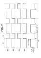
- an icon part which is a common function key button provided at the lower part of the smart device corresponds to this.
- This common function key button has, for example, three types of marks indicating “Home” (displayed by a square mark), “Back” (displayed by an arrow mark, etc.), and “Search” (displayed by a magnifying glass mark, etc.).
- “Home” displayed by a square mark
- “Back” displayed by an arrow mark, etc.
- Search displayed by a magnifying glass mark, etc.
- a capacitive information input unit using an LED light source by increasing the sensitivity of the sensor electrode, it is possible to reliably detect changes in capacitance by the sensor circuit, and to handle user input operations stably.
- an air layer having the same shape is provided between a flexible printed circuit (hereinafter abbreviated as “FPC”) on which a sensor electrode is formed and a surface panel so as to avoid a part such as an icon.
- FPC flexible printed circuit
- organic electroluminescence devices exhibit a display function by printing a mark or the like in advance on the cover glass side constituting the icon part and arranging the mark on the back side of the corresponding part.
- a touch function is indispensable when using smart devices, and capacitive touch detection type devices for touch detection are arranged on the back side of the cover glass until reaching the display unit and common function key unit. Is customary.
- a film / film type touch sensor is often used which is enlarged to the same size as the cover glass and laminated.
- a glass / glass type may be used.
- a capacitive detection method is often employed as a touch detection method.
- the anode, cathode, or metal foil layer used for protection constituting the organic electroluminescence element is the above-mentioned surface capacitance type capacitance.
- an electrostatic touch function is provided to the organic electroluminescent device, as shown in FIG.
- a touch detection electrode for touch function detection composed of a flexible printed circuit (abbreviation: FPC) with a different configuration, for example, an electrical connection unit provided with a capacitance type detection circuit and a wiring portion on a flexible substrate.
- FPC flexible printed circuit
- an organic electroluminescence element which is a light emitting device applied to the icon part, and a wiring material for controlling the driving thereof are efficiently arranged to achieve downsizing and thinning, and suitable for smart devices. There is a need for the development of luminescence modules.
- the present invention has been made in view of the above-described problems and situations, and a solution to the problem is an organic electroluminescence element having an electrode having a light emitting function and a touch detection function, a specific control circuit, and a small format. It is to provide an organic electroluminescence module capable of achieving reduction in thickness and thickness and simplification of a process, and a smart device and a lighting device including the same.
- the present inventor made any one electrode of the organic electroluminescence panel function as a touch detection electrode, a touch detection circuit unit, and a light emitting element drive circuit unit. It was found that the above-mentioned problems can be solved by an organic electroluminescence module configured to be connected to an organic electroluminescence panel, and the present invention has been achieved.
- An organic electroluminescence module having a touch detection function, A capacitive touch detection circuit unit, and a light emitting element driving circuit unit having a light emitting element driving circuit unit for driving the organic electroluminescence panel;
- the organic electroluminescence panel has a pair of planar electrodes at opposed positions inside, The pair of electrodes is connected to the light emitting element driving circuit unit; One of the pair of electrodes is a touch detection electrode, and the touch detection electrode is connected to the touch detection circuit unit.
- the light emission period of the organic electroluminescence panel controlled by the light emitting element driving circuit unit and the touch sensing period controlled by the touch detection circuit unit are separated, and the capacitance of the organic electroluminescence panel is not detected in the touch sensing period.
- at least one electrode of the pair of electrodes is in a floating potential state,
- the organic electroluminescence module according to item 1 or 2
- the light emission period of the organic electroluminescence panel controlled by the light emitting element driving circuit unit and the touch sensing period controlled by the touch detection circuit unit are separated, and the capacitance of the organic electroluminescence panel is not detected in the touch sensing period.
- the organic electroluminescence module according to item 1 or 2 wherein both of the pair of electrodes are in a floating potential state.
- the light emission period of the organic electroluminescence panel controlled by the light emitting element driving circuit unit and the touch sensing period controlled by the touch detection circuit unit are separated, and the capacitance of the organic electroluminescence panel is not detected in the touch sensing period.
- at least one of the pair of electrodes is in a floating potential state, and the pair of electrodes are in a short-circuited state,
- the light emission period of the organic electroluminescence panel controlled by the light emitting element driving circuit unit and the touch sensing period controlled by the touch detection circuit unit are separated, and the capacitance of the organic electroluminescence panel is not detected in the touch sensing period.
- the pair of electrodes are both in a floating potential state, and the pair of electrodes are in a short-circuited state.
- the organic electroluminescence panel controlled by the light emitting element driving circuit unit emits light continuously, and the touch sensing period controlled by the touch detection circuit unit is a driving method that periodically appears. 3.
- the organic electroluminescence module according to any one of claims 1 to 8, further comprising a capacitor between wirings connecting the ground of the light emitting element driving circuit unit and the touch detection circuit unit.
- a smart device comprising the organic electroluminescence module according to any one of items 1 to 9.
- An illuminating device comprising the organic electroluminescence module according to any one of items 1 to 9.
- an organic electroluminescence element having an electrode configuration having both a light emitting function and a touch detection function, a specific control circuit configuration, and achieving a small format, a thin film, and a simplified process. It is possible to provide an organic electroluminescence module that can be used, and a smart device and a lighting device including the same.
- an organic electroluminescence module applied to an icon display unit provided in a smart media is an organic electroluminescence module having a pair of electrode units disposed at opposing positions, as described in FIG. Since the luminescence panel and touch detection electrodes for touch detection, for example, a flexible printed circuit (abbreviation: FPC), are composed of an assembly in which the light emitting function and the touch detection function are separated from each other. Was an obstacle.
- FPC flexible printed circuit
- organic electroluminescence module of the present invention
- organic electroluminescence element hereinafter, abbreviated as “organic EL element”
- an anode electrode anode or a cathode electrode (cathode)
- a touch detection electrode hereinafter also simply referred to as “detection electrode”.
- the capacitance between the touch detection electrodes is Cf
- the capacitance between the anode electrode and the cathode electrode is Cel
- the capacitance at the time of touch is “Cf + Cel”.
- it is “Cel”, in the normal case, Cf ⁇ Cel, so that touch detection is difficult.
- the light emitting element driving circuit unit and the touch detection circuit unit are provided independently, and the anode electrode (in order to prevent the capacitance Cel between the anode electrode and the cathode electrode from being detected during touch detection).
- Touch detection is performed by turning off the switch between the anode) and cathode electrode (cathode) and the light emitting element driving circuit unit, and setting at least one of the anode electrode (anode) and cathode electrode (cathode) to a floating potential state.
- the floating potential state in the present invention refers to a floating potential state that is not connected to the power supply or the ground of the device, and the anode electrode (anode) or cathode electrode (cathode) at the time of touch detection has a floating potential.
- the electrostatic capacitance Cel of the organic EL panel is not detected, and as a result, touch detection by finger touch becomes possible.
- Embodiment 1 which is an example of an organic electroluminescence module Schematic circuit diagram showing an example of the configuration of a light emitting element drive circuit unit according to the present invention Timing chart showing an example of a light emission period and a sensing period in Embodiment 1 Timing chart showing another example of light emission period and sensing period (applying reverse applied voltage) in Embodiment 1 Circuit operation
- Driving circuit diagram of Embodiment 2 which is another example of the organic electroluminescence module Timing chart showing an example of a light emission period and a sensing period in Embodiment 2
- FIG. 1 is a schematic diagram for explaining a capacitance difference between a light emission period and a sensing period (at the time of a finger touch) in Embodiment 2.
- FIG. 2 is a schematic diagram for explaining a capacitance difference between a light emission period and a sensing period (at the time of finger touch) in Embodiment 2.
- Embodiment 3 which is another example of the organic electroluminescence module Timing chart showing an example of a light emission period and a sensing period in Embodiment 3 Timing chart showing another example of light emission period and sensing period (applying reverse applied voltage) in Embodiment 3 Circuit operation
- the drive circuit diagram of Embodiment 5 which is an example of an organic electroluminescence module and a cathode electrode is a touch detection
- the organic electroluminescence module of the present invention has a touch detection function, and includes a capacitive touch detection circuit unit and a light emitting element driving circuit unit having a light emitting element driving circuit unit for driving an organic electroluminescence panel.
- the organic electroluminescence panel has a pair of planar electrodes at opposing positions inside, the pair of electrodes are connected to the light emitting element driving circuit unit, and one of the pair of electrodes is A touch detection electrode, wherein the touch detection electrode is connected to the touch detection circuit unit.
- the touch detection circuit unit and the light emitting element drive circuit unit are configured to be connected to one common ground from the viewpoint that the effects of the present invention can be further manifested.
- this is a preferred embodiment from the viewpoint of designing a simplified and more efficient control circuit.
- a light emission period of the organic electroluminescence panel controlled by the light emitting element driving circuit unit and a touch sensing period controlled by the touch detection circuit unit are separated, and in the touch sensing period, the electric capacitance of the organic electroluminescence panel is It is preferable that at least one electrode of the pair of electrodes or both of the pair of electrodes is in a floating potential state so that the light emission period and the sensing period can be more clearly separated so as not to be detected.
- a light emission period of the organic electroluminescence panel controlled by the light emitting element driving circuit unit and a touch sensing period controlled by the touch detection circuit unit are separated, and in the touch sensing period, the electric capacitance of the organic electroluminescence panel is
- at least one electrode of the pair of electrodes, or both of the pair of electrodes are in a floating potential state, and the pair of electrodes are in a short-circuited state. It is preferable from the viewpoint of clear separation.
- the organic electroluminescence panel controlled by the light emitting element driving circuit unit continuously emits light
- the touch sensing period controlled by the touch detection circuit unit is a driving method that discontinuously appears to simplify the circuit. This is preferable from the viewpoint that an efficient sensing function can be developed.
- the light emission period and the sensing period can be more clearly separated by having a reverse applied voltage application period at the end of the light emission period.
- a structure including a capacitor between the wirings connecting the ground of the light emitting element driving circuit unit and the touch detection circuit unit makes the touch sensing period controlled by the touch detection circuit unit discontinuous while the light emitting element continuously emits light. It is preferable at the point which can be made to appear in.
- the organic EL element means an element composed of a pair of counter electrodes and an organic functional layer group
- the organic EL panel is sealed with a sealing resin and a sealing member with respect to the organic EL element.
- An organic EL module is a configuration in which a capacitive touch detection circuit unit and a light emitting element drive circuit unit are connected to an organic EL panel by an electrical connection member, and have both a light emitting function and a touch detection function. Have.
- the organic EL module of the present invention is an organic EL module in which an electrical connection member is joined to an organic EL panel, and as the electrical connection member, a capacitive touch detection circuit unit and the organic electroluminescence panel are driven.
- a light emitting element driving circuit unit having a light emitting element driving circuit unit, and the organic electroluminescence element constituting the organic electroluminescence panel has a pair of planar electrodes at opposed positions inside, and The electrode is connected to the light emitting element driving circuit unit, one of the pair of electrodes is a touch detection electrode, and the touch detection electrode is connected to the touch detection circuit unit.
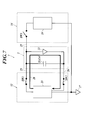
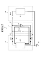
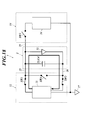
- FIG. 1 is a schematic cross-sectional view showing an example of the configuration of an organic electroluminescence module of a comparative example.
- an anode electrode (4, anode) and, for example, a hole injection layer, a hole transport layer, a light emitting layer, an electron transport layer, and an electron are formed on a transparent substrate (3).
- An organic functional layer unit (5) composed of an injection layer or the like is laminated to constitute a light emitting region.
- a cathode electrode (6, cathode) is laminated on the upper part of the organic functional layer unit (5) to constitute an organic EL element.
- the outer periphery of the organic EL element is sealed with a sealing adhesive (7), and the surface of the organic EL element is intended to prevent penetration of harmful gases (oxygen, moisture, etc.) from the external environment into the light emitting part.
- the sealing member (8) is arrange
- a light emitting element driving circuit unit (12) for controlling light emission is connected between an anode electrode (4) and a cathode electrode (6) as a pair of electrodes. Further, in a state separated from the organic EL panel (2), on the surface opposite to the surface on which the organic EL element EL element of the transparent base material (3) is formed, for example, on the flexible substrate A touch detection electrode (10) for detecting a touch function, which is constituted by an electrical connection unit (flexible printed circuit) provided with a detection circuit and a wiring portion, is provided, and its periphery is sealed with a sealing adhesive (7). The touch detection part (9) is formed, and the cover glass (11) is provided on the upper surface part.
- the touch detection electrode (10) is provided with a touch detection circuit unit (14) for detecting a touch (finger touch).
- a touch detection circuit unit (14) for detecting a touch (finger touch).
- the organic EL element and the touch detection unit (9) are configured independently of each other. It was an obstacle to formatting and thinning.
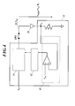
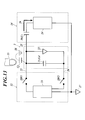
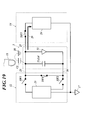
- FIG. 2 is a schematic cross-sectional view showing an example in which the anode electrode is a touch detection electrode as an example of the configuration of the organic electroluminescence module of the present invention.
- a cathode electrode (6, cathode) is laminated on the upper part of the organic functional layer unit (5) to constitute an organic EL element.
- the outer peripheral portion of the organic EL element is sealed with a sealing adhesive (7), and a sealing member (8) is disposed on the surface thereof to constitute the organic EL panel (2).
- the organic EL panel (2) according to the present invention may have a configuration having a metal foil layer on the outermost surface side for the purpose of protecting the organic EL element.
- the configuration of FIG. 2 is characterized in that the anode electrode (4A, anode) functions as a counter electrode that emits light from the organic EL element and also functions as a detection electrode that is a touch detection electrode. .
- a light emitting element driving circuit unit (12) having a light emitting element driving circuit unit for controlling light emission is connected between the anode electrode (4A) and the cathode electrode (6).
- a touch detection circuit unit (14) for detecting a touch (finger touch) is connected.
- FIG. 2 shows a configuration in which the anode electrode (4A) also serves as the detection electrode, but the function may be imparted to the cathode electrode (6A) as described later in FIG.
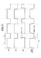
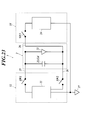
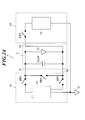
- FIG. 3 is a drive circuit diagram of Embodiment 1 which is an example of the organic EL module of the present invention.
- the organic EL panel (2) shown in the center includes an anode electrode wiring (25) connected to an anode electrode (4A, not shown), a cathode A cathode electrode wiring (26) connected to an electrode (6, not shown) is provided, and an organic EL element (22) which is a diode and a capacitor (21, Cel) are connected between the wirings.
- the anode electrode wiring (25) drawn from the anode electrode (4A, not shown) is connected to the light emitting element drive circuit section (23) via the switch 1 (SW1).
- the cathode electrode wiring (26) drawn from the cathode electrode (6, not shown) is connected to the light emitting element driving circuit section (23) via the switch 2 (SW2).
- the light emitting element driving circuit section (23) is connected to the ground (27).
- This ground (27) is specifically called a signal ground.
- the light emitting element driving circuit unit (12) incorporates a constant current driving circuit or a constant voltage driving circuit, controls the light emission timing of the organic EL element, and applies reverse bias (reverse applied voltage) as necessary. And a light emitting element driving circuit portion (23).
- the light-emitting element drive circuit unit (23) and SW1 and SW2 are shown as independent components. However, the switch 1 (SW1) is connected to the light-emitting element drive circuit unit (23) as necessary. ) And / or switch 2 (SW2) may be incorporated.
- the light emitting element driving circuit unit (12) in the present invention is the anode electrode wiring (25), SW1, the light emitting element driving circuit section (23), SW2, and the cathode electrode wiring (26) as shown by the broken line in FIG. Is a circuit range composed of
- the configuration of the light emitting element driving circuit unit (23) according to the present invention is not particularly limited, and a conventionally known light emitting element driving circuit unit (organic EL element driving circuit) can be applied.
- the light emitting element driving circuit for example, according to a preset light emission pattern of the light emitting element as shown in FIG. 5 described later, between the anode electrode and the cathode electrode, the light emission amount of the organic EL element as the light emitting element. It has a function of applying a current according to the above.
- this optical element driving circuit there is known a constant current circuit comprising a step-up or step-down DC-DC converter circuit, a current value feedback circuit, a DC-DC converter switch control circuit, and the like.
- FIG. 4 shows an example of a light emitting element driving circuit unit (23) applicable to the present invention.
- FIG. 4 is a schematic circuit diagram showing an example of a configuration of a light emitting element driving circuit unit having a light emitting element driving circuit unit according to the present invention.
- the light emitting element drive circuit section (23) includes a step-up or step-down DC-DC converter circuit (31), a switch element control circuit (32) of the DC-DC converter, and a current value feedback circuit (33).
- a step-up or step-down DC-DC converter circuit (31) when the detection resistance is R 1 and the comparison potential is V ref , the anode potential of the organic EL element (22) is DC ⁇ so that the current I OLED flowing through the organic EL element (22) becomes V ref / R 1.
- a constant current circuit can be obtained by stepping up or down the voltage by the DC converter circuit (31).
- the touch detection circuit unit (14) described on the right side detects the touch of the anode electrode wiring (25) drawn from the anode electrode (4A, not shown) functioning as the touch detection electrode via the switch 3 (SW3). Connected to the circuit unit (24), the touch detection circuit unit (24) is connected to the ground (27). A configuration in which the switch 3 (SW3) is incorporated in the touch detection circuit unit (24) may be employed.
- the touch detection circuit unit (24) is not particularly limited in its configuration, and a conventional known touch detection circuit unit can be applied.
- a touch detection circuit is composed of an amplifier, a filter, an AD converter, a rectifying / smoothing circuit, a comparator, and the like, and representative examples include a self-capacitance detection method, a series capacitance division comparison method (OMRON method), and the like.
- OMRON method series capacitance division comparison method
- the switches 1 to 3 are not particularly limited as long as they have a switching function such as an FET (field effect transistor), a TFT (thin film transistor), or the like.
- FIG. 5 is a timing chart showing an example of the light emission period and the sensing period in the first embodiment.
- the touch sensor function in the icon part can be expressed.
- the uppermost column in FIG. 5 is a chart showing the ON / OFF operation timing of SW1 in the light emitting element driving circuit unit (12), and the operation timings of SW2 and SW3 are also shown below.
- the high period indicates the ON state of the switch. The same applies to the timing charts described below.
- the lowermost column is a chart showing the history of applied voltage to the organic EL element.
- SW1 and SW2 are in the “ON” state, the voltage rises from the OLED off voltage and becomes a voltage necessary for light emission. Light emission starts.
- SW1 and SW2 are turned “OFF”, the current supply to the OLED is stopped and turned off.
- t1 and SW2 are set to “OFF”, they are not turned off instantaneously, and are turned off after a certain time (t1) according to the OLED charge / discharge time constant ⁇ .
- SW3 is a switch for controlling the drive of the touch detection circuit unit (14).
- the switch is set to “OFF”.
- the timing at which SW3 is turned “ON” is set to “ON” after a predetermined standby time (t1) has passed after turning SW1 and SW2 described above “OFF”.
- the standby period (t1) is preferably in the range of about 0 ⁇ to 5 ⁇ of the OLED charge / discharge time constant ⁇ .
- the period from when SW1 and SW2 are turned “ON” to when it is turned “OFF” is the light emission period (LT), and SW1 and SW2 are turned “OFF” and the standby time (t1 ), After SW3 is set to “ON” and touch detection is performed, the period until “OFF” is set is a sensing period (ST), and LT + ST is referred to as one frame period (1FT).
- the light emission period (LT), sensing period (ST), and one frame period (1FT) in the organic EL module of the present invention are not particularly limited, and conditions suitable for the environment to be applied can be selected as appropriate.
- As the light emission period (LT) of the OLED 0.1 to 2.0 msec.
- the sensing period (ST) is 0.05 to 0.3 msec.
- the one frame period (1FT) can be in the range of 0.15 to 2.3 msec.
- the one frame period (1FT) is preferably 60 Hz or more for the purpose of reducing flicker.
- FIG. 6 is a timing chart according to a method of applying a reverse bias applied voltage to the OLED as another example of the light emission period and the sensing period in the first embodiment.
- FIG. 7 is a circuit operation diagram showing an example of circuit operation in the light emission period (LT) of the first embodiment.
- SW3 connected to the touch detection circuit unit (14) is in an “OFF” state.
- FIG. 8 is a circuit operation diagram showing an example of circuit operation in the sensing period (ST) of the first embodiment.
- SW1 and SW2 of the light emitting element drive circuit unit (12) are turned “OFF”, the light emitting element drive circuit is opened, and the switch 3 (SW3) of the touch detection circuit unit (14) is turned “ON”.
- the switch 3 (SW3) of the touch detection circuit unit (14) is turned “ON”.
- the finger (15) and the detection electrode Capacitance (Cf) is generated between certain anode electrodes (4A).
- the capacitance (Cf) is connected to the ground (16). 29 is a touch detection information route at the time of sensing.
- FIG. 9 is a drive circuit diagram of Embodiment 2, which is another example of the organic EL module of the present invention.
- a capacitor Cs (30) is used instead of the switch (SW3) constituting the touch detection circuit unit (14) in the drive circuit diagram of the first embodiment described in FIG. It is the structure which incorporated.
- the capacitor Cs (30) By incorporating the capacitor Cs (30) into the circuit, a function similar to that of the switch 3 (SW3) can be provided.
- a configuration in which the switch 1 (SW1) or the switch 2 (SW2) is incorporated in the light emitting element driving circuit unit (23) may be employed.
- condenser Cs (30) is incorporated in the inside of a touch detection circuit part (24) may be sufficient.
- FIG. 10 is an example of a light emission period and a sensing period in Embodiment 2, and is a timing chart in which a standby time (t1) is provided as a sensing timing.
- the timing chart shown in FIG. 10 is a diagram showing the sensing timing by the capacitor Cs (30) instead of the “ON / OFF” operation of SW3 with respect to the timing chart shown in FIG. 5 described above.
- FIG. 11 is another example of the light emission period and the sensing period in Embodiment 2, and is a timing chart in which a reverse bias applied voltage is applied to a circuit operation diagram illustrating an example of circuit operation in the sensing period of Embodiment 2.
- the timing chart shown in FIG. 11 shows the sensing timing by the capacitor Cs (30) instead of the “ON / OFF” operation of SW3 with respect to the timing chart given the reverse bias application voltage shown in FIG. FIG.
- FIG. 12 is a circuit operation diagram showing an example of the circuit operation in the light emission period of Embodiment 2, which is the same as the circuit operation in the light emission period of Embodiment 1 described above with reference to FIG.
- FIG. 13 is a drive circuit operation diagram showing an example of the circuit operation in the sensing period of Embodiment 2, in which SW1 and SW2 of the light emitting element drive circuit unit (12) are set to “OFF” to open the light emitting element drive circuit.
- SW1 and SW2 of the light emitting element drive circuit unit (12) are set to “OFF” to open the light emitting element drive circuit.
- electrostatic discharge is generated between the finger (15) and the anode electrode (4A) serving as the detection electrode.
- a capacitance (Cf) is generated, and touch detection is performed based on the capacitance (Cf).
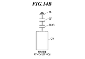
- FIG. 14A and 14B are schematic diagrams for explaining the capacitance difference between the light emission period and the sensing period (at the time of finger touch) in Embodiment 2, and as shown in FIG. 14A, in a state where the finger is not touched. Since one electrode is in a floating potential state, the capacitance Cs (30) provided in the touch detection circuit unit (14) is not detected. On the other hand, at the time of touch detection shown in FIG. 14B (at the time of finger touch), the electrostatic capacitances Cf and Cs generated between the finger (15) and the anode electrode (4A) that is the touch detection electrode are used. Since it becomes a serial composite capacitance value, a touch can be detected.
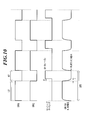
- FIG. 15 is a drive circuit diagram of Embodiment 3 which is another example of the organic EL module.
- the basic drive circuit configuration is the same as that of the drive circuit shown in FIG. 3, but the anode electrode wiring (25) and the cathode electrode wiring (26). ) Is provided with a fourth switch 4 (SW4).
- switch 1 (SW1) and / or the switch 2 (SW2) is incorporated in the light emitting element driving circuit unit (23) may be employed.
- switch 3 (SW3) is incorporated in the inside of a touch detection circuit part (24) may be sufficient.
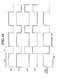
- FIG. 16 is a timing chart showing an example of a light emission period and a sensing period in the third embodiment.
- SW1 and SW2 are fully set to “ON” to cause the OLED to emit light, and the moment when the sensing period (ST) starts.
- SW1 and SW2 are turned “OFF”, and at the same time, SW3 and SW4 are turned “ON”.
- SW4 which is a short switch, the charge / discharge components remaining between the electrodes of the OLED are instantaneously removed, so that the light emission period (LT) can be obtained without providing a standby time (t1).
- the sensing period (ST) can be entered.
- FIG. 17 is another example of the light emission period and the sensing period in the embodiment 3, and is a timing chart according to a method of applying a reverse applied voltage to the OLED.
- the timing chart shown in FIG. 17 is the same as the timing chart shown in FIG. 16 except that SW1 and SW2 are turned “ON” and immediately before “OFF” at the end of the light emission period, between the anode electrode and the cathode electrode. It is a timing chart which suppressed charging / discharging at the time of OLED light extinction by giving an applied voltage (application of a reverse bias voltage).
- FIG. 18 is a drive circuit operation diagram showing an example of circuit operation in the light emission period of the third embodiment.
- the basic light emitting element driving circuit unit (12) has a circuit configuration in which SW1 and SW2 are set to “ON” and SW4 is set to “OFF”.
- the configuration is the same as that shown in FIG.
- FIG. 19 is a drive circuit operation diagram illustrating an example of circuit operation in the sensing period of Embodiment 3, in which SW1 and SW2 of the light-emitting element drive circuit unit (12) are set to “OFF” to open the light-emitting element drive circuit.
- SW1 and SW2 of the light-emitting element drive circuit unit (12) are set to “OFF” to open the light-emitting element drive circuit.
- FIG. 20 shows a sensing period in which the organic electroluminescence panel controlled by the light emitting element driving circuit unit continuously emits light and is controlled by the touch detection circuit unit (24) in Embodiment 4 which is another example of the organic electroluminescence module.
- ST is an example of a drive method in which the signal appears periodically, and a drive circuit diagram during finger feeding is illustrated. Specifically, with respect to the configuration shown in FIG. 3, SW1 and SW2 are deleted, and a capacitor (31) is provided between the wirings connecting the ground of the light emitting element drive circuit unit (23) and the touch detection circuit unit (24). It is the structure characterized by comprising.
- the light emitting element drive circuit unit (12) side is in a state where the circuit is always connected because there is no switch, and the organic EL element (22) is continuously emitting light.
- the touch detection circuit unit (14) described on the right side detects the touch of the anode electrode wiring (25) drawn from the anode electrode (4A, not shown) functioning as the touch detection electrode via the switch 3 (SW3). Connected to the circuit part (24), this touch detection circuit part is connected to the ground (27) via the capacitor (31) on the way.
- the SW3 of the touch detection circuit unit (14) is set to the “ON” state, and the upper surface of the crow substrate of the anode electrode (4), which is the detection electrode constituting the organic EL panel (2), is indicated by a finger (15 ), A capacitance (Cf) is generated between the finger (15) and an anode electrode (4A, not shown) as a detection electrode, and the touch can be detected.
- FIG. 21 is a timing chart composed of a light emission period in which light is continuously emitted in Embodiment 4 and an intermittent sensing period controlled by [ON / OFF] of SW3.
- SW1 and SW1 as shown in FIG. Since SW2 does not exist and the circuit is always connected, as shown in the lower stage, the OLED applied voltage is always “ON” and always emits light.
- touch detection can be periodically performed by turning ON / OFF SW3 of the touch detection circuit unit (14).
- touch detection electrode cathode electrode
- FIG. 22 is a schematic cross-sectional view showing an example in which the cathode electrode is a detection electrode in another configuration of the organic electroluminescence module of the present invention.
- the cathode electrode (6A) is a touch detection electrode and the cathode electrode (6A) is connected to a touch detection circuit unit. (14) is connected, and the cathode electrode (6A) surface side becomes a touch detection surface by finger eating (15).
- FIG. 23 is an example of an organic electroluminescence module, and is a drive circuit diagram of Embodiment 5 in which the cathode electrode (6A, not shown) is a touch detection electrode, and the drive of Embodiment 1 shown in FIGS.
- wiring to the touch detection circuit section (24) is made by the cathode electrode wiring (26) via SW3, and other configurations are the same as those in FIG.
- FIG. 24 is another example of the organic electroluminescence module, and is a drive circuit diagram of the embodiment 6 in which the cathode electrode is a touch detection electrode. Compared to the drive circuit diagrams of the embodiment 3 shown in FIGS.
- the wiring to the touch detection circuit part (24) is made by the cathode electrode wiring (26) through SW3, and the other configuration is exactly the same as FIG.
- Embodiment 5 and Embodiment 6 an example of a drive circuit diagram in which the cathode electrode (6A) is a detection electrode is shown.
- a configuration in which a cathode electrode is used as the touch detection electrode instead of the anode electrode can be employed.
- the organic EL panel (2) constituting the organic EL module (1) includes, for example, an anode electrode (4A, anode) and an organic functional layer unit on the transparent substrate (3) as illustrated in FIG. (5) is laminated to form a light emitting region.
- a cathode electrode (6, cathode) is laminated on the upper part of the organic functional layer unit (5) to constitute an organic EL element.
- the outer peripheral portion of the organic EL element is sealed with a sealing adhesive (7), and a sealing member (8) is arranged on the surface thereof.
- the configuration described in JP-like can be cited as an example.
- Examples of the transparent substrate (3) applicable to the organic EL element according to the present invention include transparent materials such as glass and plastic.
- Examples of the transparent substrate (3) preferably used include glass, quartz, and a resin film.
- the glass material examples include silica glass, soda lime silica glass, lead glass, borosilicate glass, and alkali-free glass.
- the glass materials from the viewpoint of imparting adhesion with adjacent layers, durability, and smoothness, if necessary, physical treatment such as polishing, formation of a thin film made of inorganic or organic matter, A hybrid thin film combining these thin films can be formed.
- polyesters such as polyethylene terephthalate (PET) and polyethylene naphthalate (PEN), polyethylene, polypropylene, cellophane, cellulose diacetate, cellulose triacetate (TAC), cellulose acetate butyrate, and cellulose acetate.
- Cellulose esters such as propionate (CAP), cellulose acetate phthalate, cellulose nitrate and their derivatives, polyvinylidene chloride, polyvinyl alcohol, polyethylene vinyl alcohol, syndiotactic polystyrene, polycarbonate, norbornene resin, polymethylpentene, poly Ether ketone, polyimide, polyethersulfone (PES), polyphenylene sulfide, Resulfones, polyetherimide, polyetherketoneimide, polyamide, fluororesin, nylon, polymethylmethacrylate, acrylic and polyarylates, Arton (trade name, manufactured by JSR) and Appel (trade name, manufactured by Mitsui Chemicals) And cycloolefin-based resins.
- CAP propionate
- CAP cellulose acetate phthalate
- cellulose nitrate and their derivatives
- polyvinylidene chloride polyvinyl alcohol
- polyethylene vinyl alcohol syndiotact
- a gas barrier layer may be provided on the transparent substrate (3) as described above, if necessary.
- the material for forming the gas barrier layer may be any material that has a function of suppressing entry of components such as moisture and oxygen that cause deterioration of the organic EL element.
- inorganic materials such as silicon oxide, silicon dioxide, and silicon nitride Can be used.
- anode electrode anode
- the anode constituting the organic EL element include metals such as Ag and Au, alloys containing metal as a main component, CuI, indium-tin composite oxide (ITO), and metal oxides such as SnO 2 and ZnO.
- metals such as Ag and Au
- alloys containing metal as a main component CuI
- metal oxides such as SnO 2 and ZnO.
- a metal or a metal-based alloy is preferable, and silver or a silver-based alloy is more preferable.
- the anode side is the light extraction side, it is necessary to be a transparent anode having optical transparency.
- the transparent anode is a layer composed mainly of silver, specifically, it may be formed of silver alone or composed of an alloy containing silver (Ag) in order to ensure the stability of silver. May be.
- alloys include silver / magnesium (Ag / Mg), silver / copper (Ag / Cu), silver / palladium (Ag / Pd), silver / palladium / copper (Ag / Pd / Cu), silver -Indium (Ag * In), silver * gold (Ag * Au), etc. are mentioned.
- the anode constituting the organic EL device according to the present invention is a transparent anode composed mainly of silver and having a thickness in the range of 2 to 20 nm.
- the thickness is preferably in the range of 4 to 12 nm.
- a thickness of 20 nm or less is preferable because the absorption component and reflection component of the transparent anode can be kept low and high light transmittance can be maintained.
- the layer composed mainly of silver means that the silver content in the transparent anode is 60% by mass or more, preferably the silver content is 80% by mass or more, More preferably, the silver content is 90% by mass or more, and particularly preferably the silver content is 98% by mass or more.
- transparent in the transparent anode according to the present invention means that the light transmittance at a wavelength of 550 nm is 50% or more.
- the transparent anode may have a configuration in which a layer composed mainly of silver is divided into a plurality of layers as necessary.
- a base layer may be provided at the lower portion from the viewpoint of improving the uniformity of the silver film of the transparent anode to be formed.
- a base layer it is a layer containing the organic compound which has a nitrogen atom or a sulfur atom, and the method of forming a transparent anode on the said base layer is a preferable aspect.
- the organic EL device has a structure in which two or more organic functional layer units each composed of an organic functional layer group and a light emitting layer are laminated between an anode and a cathode, and two or more organic functions It is possible to adopt a structure in which the layer units are separated by an intermediate electrode layer unit having independent connection terminals for obtaining electrical connection.
- the light emitting layer constituting the organic EL element preferably has a structure containing a phosphorescent compound or a fluorescent compound as a light emitting material.
- This light emitting layer is a layer that emits light by recombination of electrons injected from the electrode or the electron transport layer and holes injected from the hole transport layer, and the light emitting portion is in the layer of the light emitting layer. Alternatively, it may be the interface between the light emitting layer and the adjacent layer.
- Such a light emitting layer is not particularly limited in its configuration as long as the light emitting material contained satisfies the light emission requirements. Moreover, there may be a plurality of layers having the same emission spectrum and emission maximum wavelength. In this case, it is preferable to have a non-light emitting intermediate layer between the light emitting layers.
- the total thickness of the light emitting layers is preferably in the range of 1 to 100 nm, and more preferably in the range of 1 to 30 nm because a lower driving voltage can be obtained.
- the sum total of the thickness of a light emitting layer is the thickness also including the said intermediate
- the light emitting layer as described above is a known material such as a vacuum evaporation method, a spin coating method, a casting method, an LB method (Langmuir-Blodget, Langmuir Blodgett method), or an inkjet method. It can be formed by applying the method.
- the light emitting layer may be a mixture of a plurality of light emitting materials, and a phosphorescent light emitting material and a fluorescent light emitting material (also referred to as a fluorescent dopant or a fluorescent compound) may be mixed and used in the same light emitting layer.
- the structure of the light-emitting layer preferably includes a host compound (also referred to as a light-emitting host) and a light-emitting material (also referred to as a light-emitting dopant compound), and emits light from the light-emitting material.
- ⁇ Host compound> As the host compound contained in the light emitting layer, a compound having a phosphorescence quantum yield of phosphorescence emission at room temperature (25 ° C.) of less than 0.1 is preferable. Further, the phosphorescence quantum yield is preferably less than 0.01. Moreover, it is preferable that the volume ratio in the layer is 50% or more among the compounds contained in a light emitting layer.
- a known host compound may be used alone, or a plurality of types of host compounds may be used.
- a plurality of types of host compounds it is possible to adjust the movement of charges, and the efficiency of the organic electroluminescent device can be improved.
- a plurality of kinds of light emitting materials described later it is possible to mix different light emission, thereby obtaining an arbitrary light emission color.
- the host compound used in the light emitting layer may be a conventionally known low molecular compound or a high molecular compound having a repeating unit, and a low molecular compound having a polymerizable group such as a vinyl group or an epoxy group (evaporation polymerizable light emitting host). )
- Examples of host compounds applicable to the present invention include, for example, JP-A Nos. 2001-257076, 2001-357777, 2002-8860, 2002-43056, 2002-105445, 2002-352957, 2002-231453, 2002-234888, 2002-260861, 2002-305083, US Patent Application Publication No. 2005/0112407, US Patent Application Publication No. 2009/0030202, International Publication No. 2001/039234, International Publication No. 2008/056746, International Publication No. 2005/089025, International Publication No. 2007/063754, International Publication No. 2005/030900, International Publication 200th / No. 086,028, WO 2012/023947, can be mentioned JP 2007-254297, JP-European compounds described in Japanese Patent No. 2034538 Pat like.
- a phosphorescent compound also referred to as a phosphorescent compound, a phosphorescent material, or a phosphorescent dopant
- a fluorescent compound both a fluorescent compound or a fluorescent material
- a phosphorescent compound is a compound in which light emission from an excited triplet is observed. Specifically, it is a compound that emits phosphorescence at room temperature (25 ° C.), and the phosphorescence quantum yield is 0 at 25 ° C.
- a preferred phosphorescence quantum yield is 0.1 or more, although it is defined as 0.01 or more compounds.
- the phosphorescent quantum yield can be measured by the method described in Spectroscopic II, page 398 (1992 edition, Maruzen) of the Fourth Edition Experimental Chemistry Course 7.
- the phosphorescence quantum yield in the solution can be measured using various solvents, but when using a phosphorescent compound in the present invention, the phosphorescence quantum yield is 0.01 or more in any solvent. Should be achieved.
- the phosphorescent compound can be appropriately selected from known compounds used for the light-emitting layer of a general organic EL device, but preferably contains a group 8 to 10 metal in the periodic table of elements. More preferred are iridium compounds, more preferred are iridium compounds, osmium compounds, platinum compounds (platinum complex compounds) or rare earth complexes, and most preferred are iridium compounds.
- one light-emitting layer may contain two or more phosphorescent compounds, and the concentration ratio of the phosphorescent compound in the light-emitting layer varies in the thickness direction of the light-emitting layer. It may be a mode.
- preferred phosphorescent compounds include organometallic complexes having Ir as a central metal. More preferably, a complex containing at least one coordination mode of a metal-carbon bond, a metal-nitrogen bond, a metal-oxygen bond, and a metal-sulfur bond is preferable.
- the phosphorescent compound described above (also referred to as a phosphorescent metal complex) is described in, for example, Organic Letter, vol. 16, 2579-2581 (2001), Inorganic Chemistry, Vol. 30, No. 8, pp. 1685-1687 (1991), J. Am. Am. Chem. Soc. , 123, 4304 (2001), Inorganic Chemistry, Vol. 40, No. 7, pages 1704-1711 (2001), Inorganic Chemistry, Vol. 41, No. 12, pages 3055-3066 (2002) , New Journal of Chemistry. 26, 1171 (2002), European Journal of Organic Chemistry, Vol. 4, pages 695-709 (2004), and the methods described in these references, etc. Can be synthesized.
- Fluorescent compounds include coumarin dyes, pyran dyes, cyanine dyes, croconium dyes, squalium dyes, oxobenzanthracene dyes, fluorescein dyes, rhodamine dyes, pyrylium dyes, perylene dyes, stilbene dyes. And dyes, polythiophene dyes, and rare earth complex phosphors.
- each layer other than the light emitting layer constituting the organic functional layer unit will be described in the order of a charge injection layer, a hole transport layer, an electron transport layer, and a blocking layer.
- the charge injection layer is a layer provided between the electrode and the light emitting layer in order to lower the driving voltage and improve the light emission luminance.
- the organic EL element and its industrialization front line June 30, 1998, NT. The details are described in Volume 2, Chapter 2, “Electrode Materials” (pages 123 to 166) of “Part 2” of S Co., Ltd., and there are a hole injection layer and an electron injection layer.
- the charge injection layer is present between the anode and the light emitting layer or the hole transport layer in the case of a hole injection layer, and between the cathode and the light emitting layer or the electron transport layer in the case of an electron injection layer.
- the present invention is characterized in that the charge injection layer is disposed adjacent to the transparent electrode. When used in an intermediate electrode, it is sufficient that at least one of the adjacent electron injection layer and hole injection layer satisfies the requirements of the present invention.
- the hole injection layer is a layer disposed adjacent to the anode, which is a transparent electrode, in order to lower the driving voltage and improve the luminance of light emission.
- the organic EL element and its industrialization front line June 30, 1998 “Published by TS Co., Ltd.)”, Chapter 2, “Electrode Materials” (pages 123 to 166) in the second volume.
- JP-A-9-45479, JP-A-9-260062, JP-A-8-288069 and the like porphyrin derivatives, phthalocyanine derivatives, oxazole derivatives, oxadiazole derivatives, triazole derivatives, imidazole derivatives, pyrazoline derivatives, pyrazolone derivatives, phenylenediamine derivatives, hydrazone derivatives, stilbene derivatives, polyarylalkane derivatives, triarylamine derivatives, carbazole Derivatives, indolocarbazole derivatives, isoindole derivatives, acene derivatives such as anthracene and naphthalene, fluorene derivatives, fluorenone derivatives, polyvinylcarbazole, and aromatic amines to the main chain or side chain Polymeric material or an oligomer, polysilane, a conductive polymer or oligomer (e.
- Examples of the triarylamine derivative include benzidine type represented by ⁇ -NPD (4,4′-bis [N- (1-naphthyl) -N-phenylamino] biphenyl), and MTDATA (4,4 ′, 4 ′′).
- Examples include a starburst type represented by -tris [N- (3-methylphenyl) -N-phenylamino] triphenylamine), a compound having fluorene or anthracene in the triarylamine-linked core.
- hexaazatriphenylene derivatives such as those described in JP-T-2003-519432 and JP-A-2006-135145 can also be used as a hole transport material.
- the electron injection layer is a layer provided between the cathode and the light emitting layer for lowering the driving voltage and improving the light emission luminance.
- the cathode is composed of the transparent electrode according to the present invention
- Chapter 2 “Electrode materials” pages 123 to 166) of the second edition of “Organic EL devices and their industrialization front line (issued by NTS, November 30, 1998)” ) Is described in detail.
- Specific examples of materials preferably used for the electron injection layer As, metals represented by strontium and aluminum, alkali metal compounds represented by lithium fluoride, sodium fluoride, potassium fluoride, etc., alkali metal halide layers represented by magnesium fluoride, calcium fluoride, etc. Examples thereof include an alkaline earth metal compound layer typified by magnesium fluoride, a metal oxide typified by molybdenum oxide and aluminum oxide, and a metal complex typified by lithium-8-hydroxyquinolate (Liq).
- the transparent electrode in this invention is a cathode
- organic materials such as a metal complex
- the electron injection layer is preferably a very thin film, and depending on the constituent materials, the layer thickness is preferably in the range of 1 nm to 10 ⁇ m.
- the hole transport layer is composed of a hole transport material having a function of transporting holes.
- the hole injection layer and the electron blocking layer also have a function as a hole transport layer.
- the hole transport layer can be provided as a single layer or a plurality of layers.
- the hole transport material has any of hole injection or transport and electron barrier properties, and may be either organic or inorganic.
- triazole derivatives oxadiazole derivatives, imidazole derivatives, polyarylalkane derivatives, pyrazoline derivatives, pyrazolone derivatives, phenylenediamine derivatives, arylamine derivatives, amino-substituted chalcone derivatives, oxazole derivatives, styrylanthracene derivatives, fluorenone derivatives, hydrazone derivatives
- Examples include stilbene derivatives, silazane derivatives, aniline copolymers, conductive polymer oligomers, and thiophene oligomers.
- hole transport material those described above can be used, but porphyrin compounds, aromatic tertiary amine compounds and styrylamine compounds can be used, and in particular, aromatic tertiary amine compounds can be used. preferable.
- aromatic tertiary amine compounds and styrylamine compounds include N, N, N ′, N′-tetraphenyl-4,4′-diaminophenyl, N, N′-diphenyl-N, N′— Bis (3-methylphenyl)-[1,1′-biphenyl] -4,4′-diamine (abbreviation: TPD), 2,2-bis (4-di-p-tolylaminophenyl) propane, 1,1 -Bis (4-di-p-tolylaminophenyl) cyclohexane, N, N, N ', N'-tetra-p-tolyl-4,4'-diaminobiphenyl, 1,1-bis (4-di-p -Tolylaminophenyl) -4-phenylcyclohexane, bis (4-dimethylamino-2-methylphenyl) phenylmethane, bis (4-di-p
- the hole transport material may be formed by a known method such as a vacuum deposition method, a spin coating method, a casting method, a printing method including an ink jet method, and an LB method (Langmuir Brodget, Langmuir Brodgett method). Thus, it can be formed by thinning.
- the layer thickness of the hole transport layer is not particularly limited, but is usually about 5 nm to 5 ⁇ m, preferably 5 to 200 nm.
- the hole transport layer may have a single layer structure composed of one or more of the above materials.
- the p property can be increased by doping impurities into the material of the hole transport layer.
- Examples thereof include JP-A-4-297076, JP-A-2000-196140, JP-A-2001-102175 and J.I. Appl. Phys. 95, 5773 (2004), and the like.
- the electron transport layer is made of a material having a function of transporting electrons, and in a broad sense, the electron injection layer and the hole blocking layer also correspond to the electron transport layer.
- the electron transport layer can be provided as a single layer structure or a stacked structure of a plurality of layers.
- an electron transport material (also serving as a hole blocking material) constituting a layer portion adjacent to the light emitting layer is used as an electron transporting material. What is necessary is just to have the function to transmit.
- any one of conventionally known compounds can be selected and used. Examples include nitro-substituted fluorene derivatives, diphenylquinone derivatives, thiopyran dioxide derivatives, carbodiimides, fluorenylidenemethane derivatives, anthraquinodimethane, anthrone derivatives, and oxadiazole derivatives.
- a thiadiazole derivative in which the oxygen atom of the oxadiazole ring is substituted with a sulfur atom, and a quinoxaline derivative having a quinoxaline ring known as an electron-withdrawing group can also be used as a material for the electron transport layer. It can. Furthermore, a polymer material in which these materials are introduced into a polymer chain, or a polymer material having these materials as a polymer main chain can also be used.
- metal complexes of 8-quinolinol derivatives such as tris (8-quinolinol) aluminum (abbreviation: Alq 3 ), tris (5,7-dichloro-8-quinolinol) aluminum, tris (5,7-dibromo-8- Quinolinol) aluminum, tris (2-methyl-8-quinolinol) aluminum, tris (5-methyl-8-quinolinol) aluminum, bis (8-quinolinol) zinc (abbreviation: Znq), etc. and the central metal of these metal complexes
- a metal complex replaced with In, Mg, Cu, Ca, Sn, Ga, or Pb can also be used as a material for the electron transport layer.
- the electron transport layer can be formed by thinning the above material by a known method such as a vacuum deposition method, a spin coating method, a casting method, a printing method including an inkjet method, and an LB method.
- the thickness of the electron transport layer is not particularly limited, but is usually about 5 nm to 5 ⁇ m, preferably 5 to 200 nm.
- the electron transport layer may have a single structure composed of one or more of the above materials.
- the blocking layer includes a hole blocking layer and an electron blocking layer, and is a layer provided as necessary in addition to the constituent layers of the organic functional layer unit 3 described above.
- the blocking layer includes a hole blocking layer and an electron blocking layer, and is a layer provided as necessary in addition to the constituent layers of the organic functional layer unit 3 described above.
- Hole blocking (hole block) layers and the like are described in JP-A-11-204258, JP-A-11-204359, and “Organic EL devices and their forefront of industrialization” (published by NTS on November 30, 1998).
- the hole blocking layer has a function of an electron transport layer in a broad sense.
- the hole blocking layer is made of a hole blocking material that has a function of transporting electrons but has a very small ability to transport holes, and recombines electrons and holes by blocking holes while transporting electrons. Probability can be improved.
- the structure of an electron carrying layer can be used as a hole-blocking layer as needed.
- the hole blocking layer is preferably provided adjacent to the light emitting layer.
- the electron blocking layer has a function of a hole transport layer in a broad sense.
- the electron blocking layer is made of a material that has the ability to transport holes and has a very small ability to transport electrons. By blocking holes while transporting holes, the probability of recombination of electrons and holes is improved. Can be made.
- the structure of a positive hole transport layer can be used as an electron blocking layer as needed.
- the layer thickness of the hole blocking layer applied to the present invention is preferably in the range of 3 to 100 nm, and more preferably in the range of 5 to 30 nm.
- the cathode is an electrode film that functions to supply holes to the organic functional layer group and the light emitting layer, and a metal, an alloy, an organic or inorganic conductive compound, or a mixture thereof is used. Specifically, gold, aluminum, silver, magnesium, lithium, magnesium / copper mixture, magnesium / silver mixture, magnesium / aluminum mixture, magnesium / indium mixture, indium, lithium / aluminum mixture, rare earth metal, ITO, ZnO, TiO Oxide semiconductors such as 2 and SnO 2 .
- the cathode can be produced by forming a thin film of these conductive materials by a method such as vapor deposition or sputtering.
- the sheet resistance as the second electrode is preferably several hundred ⁇ / ⁇ or less, and the film thickness is usually selected within the range of 5 nm to 5 ⁇ m, preferably 5 to 200 nm.
- the organic EL element is a method in which emitted light is extracted also from the cathode side or a double-sided light emitting type
- a cathode having good light transmittance may be selected and configured.
- sealing member examples of the sealing means used for sealing the organic EL element include a method in which a sealing member, a cathode, and a transparent substrate are bonded with an adhesive.
- the sealing member may be disposed so as to cover the display area of the organic EL element, and may be concave or flat. Further, transparency and electrical insulation are not particularly limited.
- the sealing member include a glass plate, a polymer plate, a film, a metal plate, and a film.
- the glass plate include soda lime glass, barium / strontium-containing glass, lead glass, aluminosilicate glass, borosilicate glass, barium borosilicate glass, and quartz.
- the polymer plate include a plate made of polycarbonate, acrylic, polyethylene terephthalate, polyether sulfide, polysulfone, or the like.
- the metal plate include one or more metals or alloys selected from the group consisting of stainless steel, iron, copper, aluminum, magnesium, nickel, zinc, chromium, titanium, molybdenum, silicon, germanium, and tantalum.
- the sealing member a polymer film and a metal film can be preferably used from the viewpoint of reducing the thickness of the organic EL element. Furthermore, the polymer film has a water vapor transmission rate of 1 ⁇ 10 ⁇ 3 g / m 2 .multidot.m at a temperature of 25 ⁇ 0.5 ° C. and a relative humidity of 90 ⁇ 2% RH measured by a method according to JIS K 7129-1992.
- the oxygen permeability measured by a method according to JIS K 7126-1987 is preferably 1 ⁇ 10 ⁇ 3 ml / m 2 ⁇ 24 h ⁇ atm (1 atm is 1.01325 ⁇ 10 5 a Pa) equal to or lower than a temperature of 25 ⁇ 0.5 ° C.
- water vapor permeability at a relative humidity of 90 ⁇ 2% is preferably not more than 1 ⁇ 10 -3 g / m 2 ⁇ 24h.
- an inert gas such as nitrogen or argon, or an inert liquid such as fluorocarbon or silicon oil is injected in the gas phase and liquid phase. It is preferable to do. Further, the gap between the sealing member and the display area of the organic EL element can be evacuated, or a hygroscopic compound can be sealed in the gap.
- the manufacturing method of an organic EL element is mainly a method of forming a laminate by laminating an anode, an organic functional layer group 1, a light emitting layer, an organic functional layer group 2 and a cathode on a transparent substrate.
- a transparent substrate is prepared, and a thin film made of a desired electrode material, for example, an anode material is deposited on the transparent substrate so as to have a thickness of 1 ⁇ m or less, preferably in the range of 10 to 200 nm.
- the anode is formed by a method such as sputtering.
- a connection electrode portion (for example, an anode electrode wiring drawn from the anode electrode shown in FIG. 3) connected to an external power source is formed at the anode end portion.
- a hole injection layer and a hole transport layer constituting the organic functional layer group 1, a light emitting layer, an electron transport layer constituting the organic functional layer group 2 and the like are sequentially laminated thereon.
- Examples of the method for forming each of these layers include spin coating, casting, ink jet, vapor deposition, and printing. From the viewpoints that a homogeneous layer can be easily obtained and pinholes are not easily generated. A vacuum deposition method or a spin coating method is particularly preferable. Further, different formation methods may be applied for each layer. When a vapor deposition method is employed for forming each of these layers, the vapor deposition conditions vary depending on the type of compound used, but generally the boat heating temperature is in the range of 50 to 450 ° C.
- the degree of vacuum is 1 ⁇ 10 ⁇ 6 to Within a range of 1 ⁇ 10 ⁇ 2 Pa, a deposition rate within a range of 0.01 to 50 nm / second, a substrate temperature within a range of ⁇ 50 to 300 ° C., and a layer thickness within a range of 0.1 to 5 ⁇ m. Therefore, it is desirable to appropriately select each condition.
- a cathode is formed thereon by an appropriate forming method such as vapor deposition or sputtering. At this time, the cathode is patterned in a shape in which terminal portions are drawn from the upper side of the organic functional layer group to the periphery of the transparent substrate while maintaining an insulating state with respect to the anode by the organic functional layer group.
- the transparent base material, the anode, the organic functional layer group, the light emitting layer, and the cathode are sealed with a sealing material. That is, a sealing material that covers at least the organic functional layer group is provided on the transparent base material in a state where the terminal portions of the anode and the cathode (leading wiring of each electrode) are exposed.
- each electrode of the organic EL element is electrically connected to the light emitting element driving circuit unit (12) or the touch detection circuit unit (14).
- the electrical connection member (leading wiring) that can be used is not particularly limited as long as it is a member having conductivity, but is preferably an anisotropic conductive film (ACF), a conductive paste, or a metal paste. It is an aspect.
- anisotropic conductive film examples include a layer having fine conductive particles having conductivity mixed with a thermosetting resin.
- the conductive particle-containing layer that can be used in the present invention is not particularly limited as long as it is a layer containing conductive particles as an anisotropic conductive member, and can be appropriately selected according to the purpose.
- the conductive particles that can be used as the anisotropic conductive member according to the present invention are not particularly limited and may be appropriately selected depending on the intended purpose. Examples thereof include metal particles and metal-coated resin particles.
- Examples of commercially available ACFs include low-temperature curing ACFs that can also be applied to resin films, such as MF-331 (manufactured by Hitachi Chemical).
- the metal particles include nickel, cobalt, silver, copper, gold, palladium, and the like.
- the metal-coated resin particles for example, the surface of the resin core is any one of nickel, copper, gold, and palladium.
- the metal paste may be a commercially available metal nanoparticle paste.
- the organic electroluminescence module of the present invention is an organic electroluminescence module that can achieve small formatting and thinning, and can simplify the process, and is suitable for various smart devices and lighting devices such as smartphones and tablets. Available.
- FIG. 25 is a schematic configuration diagram showing an example of a smart device (100) having the icon portion of the organic EL module of the present invention.
- the smart device 100 of the present invention includes the organic electroluminescence module (MD) having the touch detection function described in FIGS. 3 to 24, the liquid crystal display device 120, and the like.
- a conventionally known liquid crystal display device can be used as the liquid crystal display device 120.
- FIG. 25 shows a state where the organic electroluminescence module (MD) of the present invention emits light, and the light emission of various display patterns (111) is visually recognized when viewed from the front side.
- various display patterns (111) are not visually recognized.
- the shape of the display pattern (111) shown in FIG. 25 is an example and is not limited thereto, and may be any figure, character, pattern, or the like.
- the “display pattern” means a design (design or pattern in the figure), characters, images, etc. displayed by light emission of the organic EL element.
- the organic electroluminescence module of the present invention can also be applied to a lighting device.
- the lighting device provided with the organic electroluminescence module of the present invention is also useful for display devices such as household lighting, interior lighting, and backlights of liquid crystal display devices.
- backlights such as clocks, signboard advertisements, traffic lights, light sources such as optical storage media, light sources for electrophotographic copying machines, light sources for optical communication processing machines, light sources for optical sensors, etc.
- backlights such as clocks, signboard advertisements, traffic lights, light sources such as optical storage media, light sources for electrophotographic copying machines, light sources for optical communication processing machines, light sources for optical sensors, etc.
- There are a wide range of uses such as household appliances.
- the organic electroluminescence module of the present invention can achieve a small format, a thin film, and simplified processes, and can be suitably used for various smart devices such as smartphones and tablets and lighting devices.
Abstract
Priority Applications (5)
| Application Number | Priority Date | Filing Date | Title |
|---|---|---|---|
| EP14893500.0A EP3151637B1 (fr) | 2014-05-30 | 2014-09-18 | Module électroluminescent organique, dispositif intelligent et dispositif d'éclairage |
| KR1020167004840A KR101828722B1 (ko) | 2014-05-30 | 2014-09-18 | 유기 일렉트로루미네센스 모듈, 스마트 디바이스 및 조명 장치 |
| US14/913,813 US9772095B2 (en) | 2014-05-30 | 2014-09-18 | Organic electroluminescence module, smart device, and lighting device |
| JP2016523095A JP6319434B2 (ja) | 2014-05-30 | 2014-09-18 | 有機エレクトロルミネッセンスモジュール、スマートデバイス及び照明装置 |
| CN201480047722.0A CN105519235B (zh) | 2014-05-30 | 2014-09-18 | 有机电致发光模块、智能设备以及照明装置 |
Applications Claiming Priority (2)
| Application Number | Priority Date | Filing Date | Title |
|---|---|---|---|
| JP2014-112333 | 2014-05-30 | ||
| JP2014112333 | 2014-05-30 |
Publications (1)
| Publication Number | Publication Date |
|---|---|
| WO2015182001A1 true WO2015182001A1 (fr) | 2015-12-03 |
Family
ID=54698369
Family Applications (1)
| Application Number | Title | Priority Date | Filing Date |
|---|---|---|---|
| PCT/JP2014/074697 WO2015182001A1 (fr) | 2014-05-30 | 2014-09-18 | Module électroluminescent organique, dispositif intelligent et dispositif d'éclairage |
Country Status (6)
| Country | Link |
|---|---|
| US (1) | US9772095B2 (fr) |
| EP (1) | EP3151637B1 (fr) |
| JP (1) | JP6319434B2 (fr) |
| KR (1) | KR101828722B1 (fr) |
| CN (1) | CN105519235B (fr) |
| WO (1) | WO2015182001A1 (fr) |
Cited By (5)
| Publication number | Priority date | Publication date | Assignee | Title |
|---|---|---|---|---|
| WO2017154278A1 (fr) * | 2016-03-11 | 2017-09-14 | コニカミノルタ株式会社 | Module électroluminescent organique, dispositif intelligent et dispositif d'éclairage |
| WO2018051708A1 (fr) * | 2016-09-13 | 2018-03-22 | コニカミノルタ株式会社 | Dispositif d'éclairage |
| WO2018101385A1 (fr) * | 2016-11-30 | 2018-06-07 | コニカミノルタ株式会社 | Dispositif électronique |
| WO2018168617A1 (fr) * | 2017-03-16 | 2018-09-20 | コニカミノルタ株式会社 | Dispositif d'émission de lumière plane |
| EP3392561A4 (fr) * | 2015-12-17 | 2019-06-05 | Kaneka Corporation | Système d'éclairage et source de lumière planaire |
Families Citing this family (6)
| Publication number | Priority date | Publication date | Assignee | Title |
|---|---|---|---|---|
| US8866708B2 (en) * | 2011-01-21 | 2014-10-21 | Peter Sui Lun Fong | Light emitting diode switch device and array |
| CN104835454B (zh) * | 2015-06-01 | 2017-10-10 | 京东方科技集团股份有限公司 | 一种有机电致发光触控面板、其驱动方法显示装置 |
| DE102015110075A1 (de) * | 2015-06-23 | 2016-12-29 | Osram Oled Gmbh | Anordnung zum Betreiben eines organischen strahlungsemittierenden Bauelements |
| JP6556812B2 (ja) * | 2017-11-28 | 2019-08-07 | Nissha株式会社 | ハードコート付フィルムタイプタッチセンサとこれを用いたフレキシブルディバイス |
| CN108224148B (zh) * | 2018-01-04 | 2023-04-18 | 京东方科技集团股份有限公司 | 一种oled照明面板及其驱动方法,照明装置 |
| TWI750700B (zh) * | 2020-06-18 | 2021-12-21 | 友達光電股份有限公司 | 觸控顯示裝置 |
Citations (6)
| Publication number | Priority date | Publication date | Assignee | Title |
|---|---|---|---|---|
| JP2005537610A (ja) * | 2001-11-20 | 2005-12-08 | タッチセンサー テクノロジーズ,エルエルシー | 統合されたタッチ・センサおよび発光装置 |
| JP2007534070A (ja) * | 2004-04-22 | 2007-11-22 | ソニー エリクソン モバイル コミュニケーションズ, エービー | 電子機器のための制御インタフェース装置 |
| WO2010032329A1 (fr) * | 2008-09-22 | 2010-03-25 | パイオニア株式会社 | Dispositif photoémetteur électroluminescent |
| JP2011514700A (ja) * | 2008-01-29 | 2011-05-06 | コーニンクレッカ フィリップス エレクトロニクス エヌ ヴィ | 組み込まれた近接センサを備えるoled照明装置 |
| JP2012502421A (ja) * | 2008-09-08 | 2012-01-26 | コーニンクレッカ フィリップス エレクトロニクス エヌ ヴィ | 静電容量近接性感知手段を有するoled |
| JP2012504811A (ja) * | 2008-10-01 | 2012-02-23 | コーニンクレッカ フィリップス エレクトロニクス エヌ ヴィ | Oledデバイス及び電子回路 |
Family Cites Families (11)
| Publication number | Priority date | Publication date | Assignee | Title |
|---|---|---|---|---|
| JP5664369B2 (ja) | 2011-03-15 | 2015-02-04 | オムロン株式会社 | 面光源装置 |
| US9310947B2 (en) * | 2011-07-29 | 2016-04-12 | Sharp Kabushiki Kaisha | Display device |
| JP2013065429A (ja) | 2011-09-16 | 2013-04-11 | Nec Casio Mobile Communications Ltd | 静電容量式情報入力ユニット、携帯型端末装置、及び静電容量式情報入力ユニットの製造方法 |
| US9529479B2 (en) * | 2011-10-14 | 2016-12-27 | Hung-Ta LIU | Touch sensing method, module, and display |
| KR101416003B1 (ko) * | 2012-06-20 | 2014-07-08 | 엘지디스플레이 주식회사 | 터치스크린 일체형 표시장치 및 그 구동 방법 |
| KR101469485B1 (ko) * | 2012-08-13 | 2014-12-05 | 엘지디스플레이 주식회사 | 유기 발광 표시 장치 및 이의 제조 방법 |
| US9092088B2 (en) * | 2012-08-16 | 2015-07-28 | Eastman Kodak Company | Pixel-aligned ground micro-wire device |
| TWI494676B (zh) * | 2012-11-22 | 2015-08-01 | Innocom Tech Shenzhen Co Ltd | 觸控顯示裝置及其驅動方法 |
| JP6057462B2 (ja) * | 2013-01-24 | 2017-01-11 | シナプティクス・ジャパン合同会社 | 半導体装置 |
| JP6245102B2 (ja) * | 2014-07-23 | 2017-12-13 | コニカミノルタ株式会社 | 有機エレクトロルミネッセンスモジュール及び有機エレクトロルミネッセンスモジュールの製造方法 |
| EP3187983A4 (fr) * | 2014-08-25 | 2018-04-18 | Konica Minolta, Inc. | Module électroluminescent organique, dispositif intelligent, et appareil d'éclairage |
-
2014
- 2014-09-18 JP JP2016523095A patent/JP6319434B2/ja active Active
- 2014-09-18 EP EP14893500.0A patent/EP3151637B1/fr active Active
- 2014-09-18 CN CN201480047722.0A patent/CN105519235B/zh active Active
- 2014-09-18 KR KR1020167004840A patent/KR101828722B1/ko active IP Right Grant
- 2014-09-18 WO PCT/JP2014/074697 patent/WO2015182001A1/fr active Application Filing
- 2014-09-18 US US14/913,813 patent/US9772095B2/en active Active
Patent Citations (6)
| Publication number | Priority date | Publication date | Assignee | Title |
|---|---|---|---|---|
| JP2005537610A (ja) * | 2001-11-20 | 2005-12-08 | タッチセンサー テクノロジーズ,エルエルシー | 統合されたタッチ・センサおよび発光装置 |
| JP2007534070A (ja) * | 2004-04-22 | 2007-11-22 | ソニー エリクソン モバイル コミュニケーションズ, エービー | 電子機器のための制御インタフェース装置 |
| JP2011514700A (ja) * | 2008-01-29 | 2011-05-06 | コーニンクレッカ フィリップス エレクトロニクス エヌ ヴィ | 組み込まれた近接センサを備えるoled照明装置 |
| JP2012502421A (ja) * | 2008-09-08 | 2012-01-26 | コーニンクレッカ フィリップス エレクトロニクス エヌ ヴィ | 静電容量近接性感知手段を有するoled |
| WO2010032329A1 (fr) * | 2008-09-22 | 2010-03-25 | パイオニア株式会社 | Dispositif photoémetteur électroluminescent |
| JP2012504811A (ja) * | 2008-10-01 | 2012-02-23 | コーニンクレッカ フィリップス エレクトロニクス エヌ ヴィ | Oledデバイス及び電子回路 |
Non-Patent Citations (1)
| Title |
|---|
| See also references of EP3151637A4 * |
Cited By (10)
| Publication number | Priority date | Publication date | Assignee | Title |
|---|---|---|---|---|
| EP3392561A4 (fr) * | 2015-12-17 | 2019-06-05 | Kaneka Corporation | Système d'éclairage et source de lumière planaire |
| WO2017154278A1 (fr) * | 2016-03-11 | 2017-09-14 | コニカミノルタ株式会社 | Module électroluminescent organique, dispositif intelligent et dispositif d'éclairage |
| WO2018051708A1 (fr) * | 2016-09-13 | 2018-03-22 | コニカミノルタ株式会社 | Dispositif d'éclairage |
| KR20190042692A (ko) | 2016-09-13 | 2019-04-24 | 코니카 미놀타 가부시키가이샤 | 조명 장치 |
| CN109690185A (zh) * | 2016-09-13 | 2019-04-26 | 柯尼卡美能达株式会社 | 照明装置 |
| EP3514452A4 (fr) * | 2016-09-13 | 2019-07-24 | Konica Minolta, Inc. | Dispositif d'éclairage |
| US10785846B2 (en) | 2016-09-13 | 2020-09-22 | Konica Minolta, Inc. | Illumination device |
| CN109690185B (zh) * | 2016-09-13 | 2020-12-29 | 柯尼卡美能达株式会社 | 照明装置 |
| WO2018101385A1 (fr) * | 2016-11-30 | 2018-06-07 | コニカミノルタ株式会社 | Dispositif électronique |
| WO2018168617A1 (fr) * | 2017-03-16 | 2018-09-20 | コニカミノルタ株式会社 | Dispositif d'émission de lumière plane |
Also Published As
| Publication number | Publication date |
|---|---|
| CN105519235B (zh) | 2017-05-10 |
| JP6319434B2 (ja) | 2018-05-09 |
| US20160363304A1 (en) | 2016-12-15 |
| KR101828722B1 (ko) | 2018-02-12 |
| US9772095B2 (en) | 2017-09-26 |
| KR20160039231A (ko) | 2016-04-08 |
| EP3151637A1 (fr) | 2017-04-05 |
| JPWO2015182001A1 (ja) | 2017-04-20 |
| CN105519235A (zh) | 2016-04-20 |
| EP3151637A4 (fr) | 2018-01-17 |
| EP3151637B1 (fr) | 2021-09-08 |
Similar Documents
| Publication | Publication Date | Title |
|---|---|---|
| JP6708124B2 (ja) | 有機エレクトロルミネッセンスモジュール、スマートデバイス及び照明装置 | |
| JP6319434B2 (ja) | 有機エレクトロルミネッセンスモジュール、スマートデバイス及び照明装置 | |
| JP6365665B2 (ja) | 有機エレクトロルミネッセンスモジュール、スマートデバイス及び照明装置 | |
| JP6477683B2 (ja) | 有機エレクトロルミネッセンスモジュール及びスマートデバイス | |
| JP6801664B2 (ja) | 有機エレクトロルミネッセンスモジュール、スマートデバイス及び照明装置 | |
| JP6741062B2 (ja) | 有機エレクトロルミネッセンスモジュール、スマートデバイス及び照明装置 | |
| WO2016181704A1 (fr) | Module électroluminescent organique et dispositif intelligent | |
| JP2016099921A (ja) | 有機エレクトロルミネッセンスモジュール、並びにこれを備えたスマートデバイス及び照明装置 | |
| JP6881566B2 (ja) | 面発光装置 | |
| WO2018123887A1 (fr) | Affichage électroluminescent organique à matrice passive et procédé de détection tactile |
Legal Events
| Date | Code | Title | Description |
|---|---|---|---|
| ENP | Entry into the national phase |
Ref document number: 2016523095 Country of ref document: JP Kind code of ref document: A |
|
| 121 | Ep: the epo has been informed by wipo that ep was designated in this application |
Ref document number: 14893500 Country of ref document: EP Kind code of ref document: A1 |
|
| REEP | Request for entry into the european phase |
Ref document number: 2014893500 Country of ref document: EP |
|
| WWE | Wipo information: entry into national phase |
Ref document number: 2014893500 Country of ref document: EP |
|
| WWE | Wipo information: entry into national phase |
Ref document number: 14913813 Country of ref document: US |
|
| ENP | Entry into the national phase |
Ref document number: 20167004840 Country of ref document: KR Kind code of ref document: A |
|
| NENP | Non-entry into the national phase |
Ref country code: DE |