WO2015178196A1 - 圧電薄膜及び圧電薄膜素子 - Google Patents
圧電薄膜及び圧電薄膜素子 Download PDFInfo
- Publication number
- WO2015178196A1 WO2015178196A1 PCT/JP2015/063119 JP2015063119W WO2015178196A1 WO 2015178196 A1 WO2015178196 A1 WO 2015178196A1 JP 2015063119 W JP2015063119 W JP 2015063119W WO 2015178196 A1 WO2015178196 A1 WO 2015178196A1
- Authority
- WO
- WIPO (PCT)
- Prior art keywords
- thin film
- piezoelectric thin
- piezoelectric
- electric field
- plane
- Prior art date
- Legal status (The legal status is an assumption and is not a legal conclusion. Google has not performed a legal analysis and makes no representation as to the accuracy of the status listed.)
- Ceased
Links
Images



Classifications
-
- H—ELECTRICITY
- H10—SEMICONDUCTOR DEVICES; ELECTRIC SOLID-STATE DEVICES NOT OTHERWISE PROVIDED FOR
- H10N—ELECTRIC SOLID-STATE DEVICES NOT OTHERWISE PROVIDED FOR
- H10N30/00—Piezoelectric or electrostrictive devices
- H10N30/80—Constructional details
- H10N30/85—Piezoelectric or electrostrictive active materials
- H10N30/853—Ceramic compositions
- H10N30/8542—Alkali metal based oxides, e.g. lithium, sodium or potassium niobates
-
- C—CHEMISTRY; METALLURGY
- C01—INORGANIC CHEMISTRY
- C01G—COMPOUNDS CONTAINING METALS NOT COVERED BY SUBCLASSES C01D OR C01F
- C01G33/00—Compounds of niobium
- C01G33/006—Compounds containing niobium, with or without oxygen or hydrogen, and containing two or more other elements
-
- C—CHEMISTRY; METALLURGY
- C23—COATING METALLIC MATERIAL; COATING MATERIAL WITH METALLIC MATERIAL; CHEMICAL SURFACE TREATMENT; DIFFUSION TREATMENT OF METALLIC MATERIAL; COATING BY VACUUM EVAPORATION, BY SPUTTERING, BY ION IMPLANTATION OR BY CHEMICAL VAPOUR DEPOSITION, IN GENERAL; INHIBITING CORROSION OF METALLIC MATERIAL OR INCRUSTATION IN GENERAL
- C23C—COATING METALLIC MATERIAL; COATING MATERIAL WITH METALLIC MATERIAL; SURFACE TREATMENT OF METALLIC MATERIAL BY DIFFUSION INTO THE SURFACE, BY CHEMICAL CONVERSION OR SUBSTITUTION; COATING BY VACUUM EVAPORATION, BY SPUTTERING, BY ION IMPLANTATION OR BY CHEMICAL VAPOUR DEPOSITION, IN GENERAL
- C23C14/00—Coating by vacuum evaporation, by sputtering or by ion implantation of the coating forming material
- C23C14/06—Coating by vacuum evaporation, by sputtering or by ion implantation of the coating forming material characterised by the coating material
- C23C14/08—Oxides
- C23C14/088—Oxides of the type ABO3 with A representing alkali, alkaline earth metal or Pb and B representing a refractory or rare earth metal
-
- H—ELECTRICITY
- H10—SEMICONDUCTOR DEVICES; ELECTRIC SOLID-STATE DEVICES NOT OTHERWISE PROVIDED FOR
- H10N—ELECTRIC SOLID-STATE DEVICES NOT OTHERWISE PROVIDED FOR
- H10N30/00—Piezoelectric or electrostrictive devices
- H10N30/704—Piezoelectric or electrostrictive devices based on piezoelectric or electrostrictive films or coatings
-
- H—ELECTRICITY
- H10—SEMICONDUCTOR DEVICES; ELECTRIC SOLID-STATE DEVICES NOT OTHERWISE PROVIDED FOR
- H10N—ELECTRIC SOLID-STATE DEVICES NOT OTHERWISE PROVIDED FOR
- H10N30/00—Piezoelectric or electrostrictive devices
- H10N30/704—Piezoelectric or electrostrictive devices based on piezoelectric or electrostrictive films or coatings
- H10N30/706—Piezoelectric or electrostrictive devices based on piezoelectric or electrostrictive films or coatings characterised by the underlying bases, e.g. substrates
-
- H—ELECTRICITY
- H10—SEMICONDUCTOR DEVICES; ELECTRIC SOLID-STATE DEVICES NOT OTHERWISE PROVIDED FOR
- H10N—ELECTRIC SOLID-STATE DEVICES NOT OTHERWISE PROVIDED FOR
- H10N30/00—Piezoelectric or electrostrictive devices
- H10N30/80—Constructional details
- H10N30/85—Piezoelectric or electrostrictive active materials
- H10N30/853—Ceramic compositions
-
- H—ELECTRICITY
- H10—SEMICONDUCTOR DEVICES; ELECTRIC SOLID-STATE DEVICES NOT OTHERWISE PROVIDED FOR
- H10N—ELECTRIC SOLID-STATE DEVICES NOT OTHERWISE PROVIDED FOR
- H10N30/00—Piezoelectric or electrostrictive devices
- H10N30/80—Constructional details
- H10N30/87—Electrodes or interconnections, e.g. leads or terminals
-
- C—CHEMISTRY; METALLURGY
- C01—INORGANIC CHEMISTRY
- C01P—INDEXING SCHEME RELATING TO STRUCTURAL AND PHYSICAL ASPECTS OF SOLID INORGANIC COMPOUNDS
- C01P2002/00—Crystal-structural characteristics
- C01P2002/70—Crystal-structural characteristics defined by measured X-ray, neutron or electron diffraction data
- C01P2002/72—Crystal-structural characteristics defined by measured X-ray, neutron or electron diffraction data by d-values or two theta-values, e.g. as X-ray diagram
-
- C—CHEMISTRY; METALLURGY
- C01—INORGANIC CHEMISTRY
- C01P—INDEXING SCHEME RELATING TO STRUCTURAL AND PHYSICAL ASPECTS OF SOLID INORGANIC COMPOUNDS
- C01P2002/00—Crystal-structural characteristics
- C01P2002/70—Crystal-structural characteristics defined by measured X-ray, neutron or electron diffraction data
- C01P2002/74—Crystal-structural characteristics defined by measured X-ray, neutron or electron diffraction data by peak-intensities or a ratio thereof only
-
- C—CHEMISTRY; METALLURGY
- C01—INORGANIC CHEMISTRY
- C01P—INDEXING SCHEME RELATING TO STRUCTURAL AND PHYSICAL ASPECTS OF SOLID INORGANIC COMPOUNDS
- C01P2006/00—Physical properties of inorganic compounds
- C01P2006/40—Electric properties
-
- H—ELECTRICITY
- H10—SEMICONDUCTOR DEVICES; ELECTRIC SOLID-STATE DEVICES NOT OTHERWISE PROVIDED FOR
- H10N—ELECTRIC SOLID-STATE DEVICES NOT OTHERWISE PROVIDED FOR
- H10N30/00—Piezoelectric or electrostrictive devices
- H10N30/01—Manufacture or treatment
- H10N30/07—Forming of piezoelectric or electrostrictive parts or bodies on an electrical element or another base
- H10N30/074—Forming of piezoelectric or electrostrictive parts or bodies on an electrical element or another base by depositing piezoelectric or electrostrictive layers, e.g. aerosol or screen printing
- H10N30/076—Forming of piezoelectric or electrostrictive parts or bodies on an electrical element or another base by depositing piezoelectric or electrostrictive layers, e.g. aerosol or screen printing by vapour phase deposition
Definitions
- the present invention relates to a potassium sodium niobate-based piezoelectric thin film and a piezoelectric thin film element using the piezoelectric thin film.
- a piezoelectric material made of potassium sodium niobate having a perovskite crystal structure has attracted attention as a lead-free piezoelectric magnetic composition.
- Patent Document 1 a composition represented by the general formula: (1-n) (K 1-xy Na x Li y ) m (Nb 1-z Ta z ) O 3 -nM1M2O 3 is mainly used.
- a piezoelectric magnetic composition as a component is disclosed.
- m, n, x, y, and z are 0.98 ⁇ m ⁇ 1.0, 0 ⁇ n ⁇ 0.1, 0.1 ⁇ x, y ⁇ 0.3, and x + y ⁇ 0, respectively. .75 and 0 ⁇ z ⁇ 0.3.
- An object of the present invention is to provide a piezoelectric thin film and a piezoelectric thin film element in which deterioration of piezoelectric characteristics hardly occurs.
- the piezoelectric thin film according to the present invention is a piezoelectric thin film containing potassium sodium niobate represented by the general formula (1): (K 1-x Na x ) NbO 3 and CaTiO 3 ,
- the lattice plane interval calculated from the diffraction peak of the (001) plane is 3.975 mm or less
- the diffraction peak intensity I 101 of the (101) plane in the X-ray diffraction profile of the piezoelectric thin film is The ratio I 101 / I 001 to the diffraction peak intensity I 001 of the (001) plane satisfies log 10 (I 101 / I 001 ) ⁇ ⁇ 2.10.
- the ratio of the diffraction peak intensity I 101 on the ( 101 ) plane to the diffraction peak intensity I 001 on the (001) plane is I 101 / I 001.
- log 10 (I 101 / I 001 ) ⁇ ⁇ 2.95 is satisfied.
- the piezoelectric thin film according to the present invention is preferably a piezoelectric thin film containing potassium sodium niobate represented by the above general formula (1): (K 1-x Na x ) NbO 3 and CaTiO 3. 2): (1-n) (K 1-x Na x ) A piezoelectric thin film containing a composition represented by NbO 3 —nCaTiO 3 , wherein x and n in the general formula (2) are 0.56 ⁇ x ⁇ 0.73 and 0.02 ⁇ n ⁇ 0.073.
- the piezoelectric thin film element according to the present invention includes a substrate, the piezoelectric thin film according to the present invention provided on the substrate, and first and second electrodes provided so as to sandwich the piezoelectric thin film.
- the present invention it is possible to provide a piezoelectric thin film and a piezoelectric thin film element in which deterioration of piezoelectric characteristics hardly occurs.
- FIG. 1 is a schematic front sectional view of a piezoelectric thin film element according to an embodiment of the present invention.
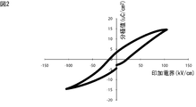
- FIG. 2 is a diagram showing a PE hysteresis curve of a piezoelectric thin film containing conventional KNN-CT.
- FIG. 3 is a PE hysteresis curve of a piezoelectric thin film according to an embodiment of the present invention.
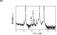
- FIG. 4 is a diagram showing an X-ray diffraction profile of a piezoelectric thin film manufactured in an experimental example.
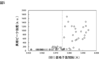
- FIG. 5 is a graph showing the relationship between the lattice spacing of the (001) plane in the X-ray diffraction profile of FIG. 4 and the peak intensity of the different phase.
- FIG. 1 is a schematic front sectional view of a piezoelectric thin film element according to an embodiment of the present invention.
- FIG. 2 is a diagram showing a PE hysteresis curve of a piezoelectric thin film containing conventional KNN
- FIG. 6 shows the relationship between the coercive electric field and the ratio I 101 / I 001 of the (101) plane diffraction peak intensity I 101 to the (001) plane diffraction peak intensity I 001 in the X-ray diffraction profile of FIG.
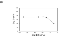
- FIG. 7 is a graph showing the applied electric field dependence of the piezoelectric constant
- FIG. 1 is a schematic front sectional view of a piezoelectric thin film element according to an embodiment of the present invention.
- the piezoelectric thin film element 1 includes a substrate 2.
- the substrate 2 is made of Si. But the board
- substrate 2 may be formed with metal materials, such as glass, SOI, another semiconductor material, a single crystal material, stainless steel, and titanium.
- An SiO 2 film 6 is formed on the substrate 2.
- a first electrode 4 (to be described later) and a material for forming the substrate 2 can be electrically insulated.
- the SiO 2 film 6 may not be provided.
- a first electrode 4 is provided on the SiO 2 film 6. More specifically, the first electrode 4 is laminated on the SiO 2 film 6 via the first adhesion layer 7.
- the first electrode 4 is desirably formed of a material that is stable even in a high-temperature oxygen atmosphere. As such a material, for example, a noble metal material such as Pt, Au, or Ir or a conductive oxide material is used. In the present embodiment, the first electrode 4 is made of Pt.
- the first adhesion layer 7 is made of Ti.
- the first adhesion layer 7 may be formed of a material such as TiO x having a function as an adhesion layer.
- a piezoelectric thin film 3 is stacked on the first electrode 4.
- the piezoelectric thin film 3 includes potassium sodium niobate represented by the general formula (1): (K 1-x Na x ) NbO 3 and CaTiO 3 .
- a second electrode 5 is formed on the piezoelectric thin film 3. More specifically, the second electrode 5 is laminated on the piezoelectric thin film 3 via the second adhesion layer 8.
- the second electrode 5 is made of Pt. But the 2nd electrode 5 may be comprised with other appropriate electroconductive materials.
- the second adhesion layer 8 is made of Ti.
- the second adhesion layer 8 may be formed of a material such as TiO x having a function as an adhesion layer.
- the first and second adhesion layers 7 and 8 may not be provided. That is, the piezoelectric thin film 3 may be formed so as to be directly sandwiched between the first and second electrodes 4 and 5.
- the piezoelectric thin film according to the present invention includes potassium sodium niobate (KNN) represented by the general formula (1): (K 1-x Na x ) NbO 3 and CaTiO 3 .
- KNN potassium sodium niobate
- the piezoelectric thin film containing KNN and CaTiO 3 includes a composition (KNN-CT) represented by the general formula (2): (1-n) (K 1-x Na x ) NbO 3 -nCaTiO 3
- a piezoelectric thin film is preferably used.
- the lattice spacing calculated from the diffraction peak of the (001) plane in the X-ray diffraction profile of the piezoelectric thin film is 3.975 mm or less. Therefore, the generation of a different phase other than the perovskite phase is suppressed.
- the X-ray diffraction profile is measured by performing a 2 ⁇ / ⁇ scan in out-of-plane with respect to the piezoelectric thin film.
- the piezoelectric thin film according to the present invention hardly deteriorates in piezoelectric characteristics even when driven at a low electric field. This will be specifically described with reference to FIGS.
- the applied electric field is weakened from the saturation state, the polarization state is released in order from the domain where the polarization inversion is difficult.
- the electric field applied in the negative direction is further increased, the polarization of the entire piezoelectric thin film becomes zero.
- the electric field when the polarization becomes zero in the entire piezoelectric thin film is called a coercive electric field.
- the coercive electric field when polarized in the positive direction takes a negative value
- the coercive electric field when polarized in the negative direction is Takes a positive value.
- the polarization state is saturated in the negative direction.
- the case where the electric field in the negative direction is weakened and the electric field in the positive direction is strengthened is described in the same manner as the case where the electric field in the positive direction is weakened and the electric field in the negative direction is strengthened.
- the peak intensity ratio I 101 / I 001 of the X-ray diffraction profile satisfies log 10 (I 101 / I 001 ) ⁇ ⁇ 2.10.
- the coercive electric field which normally exists in positive and negative symmetry, has a PE hysteresis curve in which it is biased in the positive direction. That is, in the piezoelectric thin film according to the present invention, the negative remanent polarization value is large. Therefore, the piezoelectric thin film according to the present invention hardly deteriorates in piezoelectric characteristics even in a low electric field and no electric field application region.
- the bias in the positive direction is further increased, that is, the peak intensity ratio I 101 / I 001 of the X-ray diffraction profile is set to log 10 (I 101 / I
- any coercive electric field that normally exists in positive and negative symmetry can be set to a positive value. That is, by further increasing the bias in the positive direction, it is possible to spontaneously polarize in the negative direction.
- the piezoelectric thin film is polarized in a direction opposite to the direction in which the coercive electric field is biased when it is formed. Therefore, it is possible to omit the polarization step at the time of film formation, which was conventionally necessary.
- a device using a piezoelectric thin film is mounted by reflow at a temperature at which the polarization of the piezoelectric magnetic composition disappears, that is, about 300 ° C., but is spontaneously polarized in the negative direction as described above. In some cases, the piezoelectric characteristics are unlikely to deteriorate after reflow.
- x and n in the general formula (2): (1-n) (K 1-x Na x ) NbO 3 —nCaTiO 3 are 0.56 ⁇ x ⁇ 0.73 and 0.02 ⁇ n. It is preferable to be in the range of ⁇ 0.073.
- the heterogeneous phase can be further reduced, and the piezoelectric characteristics can be enhanced more effectively.
- a first adhesion layer made of Ti and a first electrode made of Pt were formed in this order on a Si substrate on which a SiO 2 film was formed.
- a piezoelectric thin film containing KNN-CT was formed on the first electrode.
- a buffer layer for controlling orientation and stress may be provided between the first electrode and the piezoelectric thin film.
- the material for forming the buffer layer include perovskite oxide materials such as LaNiO 3 and SrRuO 3 and potassium sodium niobate (KNN) thin films formed at low temperatures.
- the piezoelectric thin film was formed by RF magnetron sputtering.
- a single target may be used, or a plurality of targets may be simultaneously sputtered to obtain a target composition.
- the substrate heating temperature during sputtering was set to 500 ° C. to 650 ° C. at the apparatus setting temperature, and was performed in a mixed gas atmosphere of Ar and O 2 .
- the ratio O 2 / (Ar + O 2 ) between Ar and O 2 in the mixed gas was adjusted to be approximately 1 to 10%.
- the sputtering pressure was 0.3 Pa.
- the cathode power per unit area was 2.5 W / cm 2 and the film formation time was adjusted so that the film thickness of the formed piezoelectric thin film was 1 to 3 ⁇ m.
- the value of m of the formed piezoelectric thin film was 0.85 ⁇ m ⁇ 0.90.
- the values of x and n of the formed piezoelectric thin film were 0.56 ⁇ x ⁇ 0.73 and 0.02 ⁇ n ⁇ 0.043, respectively.
- a piezoelectric thin film element was obtained by forming a second adhesion layer made of Ti and a second electrode made of Pt in this order on the piezoelectric thin film.
- FIG. 4 is a diagram showing an X-ray diffraction profile of the produced piezoelectric thin film.
- the Miller index is expressed assuming that the crystal structure of KNN-CT contained in the piezoelectric thin film is a pseudo-cubic crystal.
- the lattice spacing was calculated from the diffraction angle of the diffraction peak of the (001) plane, and the lattice spacing of the (001) plane was 3.952 mm to 3.994 mm.
- FIG. 5 is a graph showing the relationship between the lattice spacing of the (001) plane in the X-ray diffraction profile of FIG. 4 and the peak intensity of the different phase.
- the peak intensity of the different phase was too weak to observe the peak, that is, in the case of a good quality piezoelectric thin film with few different phases, the background intensity was measured as the peak intensity of the different phase.
- the ferroelectric characteristics of the sample having a lattice spacing of (001) plane in FIG. Specifically, a PE hysteresis measurement was performed on the first electrode to measure a change in polarization value when an electric field was applied from the second electrode. At this time, an electric field of 106 kV / cm at the maximum was applied as a triangular wave of 100 Hz in order in both positive and negative directions. Before sweeping the triangular wave, a polarization pulse electric field of 106 kV / cm was applied.
- the coercive electric field E C ⁇ existing on the negative electric field side has a value of ⁇ 17.2 to 3. It was 7 kV / cm.
- the value of the coercive electric field E C + existing on the positive electrode side was 12.5 to 38.4 kV / cm.
- FIG. 6 is a diagram showing the relationship between log 10 (I 101 / I 001 ) and the obtained coercive electric field.
- FIG. 7 is a graph showing the applied electric field dependence of the piezoelectric constant
- was obtained from the displacement of the tip of the unimorph cantilever when a cantilever unimorph cantilever composed of a piezoelectric thin film and a Si substrate was produced and an electric field was applied in the thickness direction of the piezoelectric thin film. .
- in this experimental example is the same as that of JP 2012-019050 A.
- the Young's modulus of the piezoelectric thin film was the same as the bulk KNN value.
- FIG. 7 shows that a sufficiently high piezoelectric constant
- is very low when the applied electric field is driven at a low electric field of about 10 kV / cm.
- Piezoelectric thin film devices using piezoelectric thin films are often driven by a low electric field. At least, the upper limit of the drive voltage obtained from a general circuit is about 5 V. If the film thickness of the piezoelectric thin film is 3 ⁇ m, the electric field that can be applied is about 17 kV / cm.
- the coercive electric field of the piezoelectric thin film can be biased by 13 kV / cm or more, that is, if the amount of bias of the piezoelectric thin film can be made 13 kV / cm or more, it is as if the electric field that can be applied from the circuit is 17 kV / cm.
- the piezoelectric thin film can be driven as if an electric field of 30 kV / cm is applied.
- I 101 / I 001 is log 10 (I 101 / I 001 ) ⁇ ⁇ 2 It can be seen that it should be in the range of .10.
- the ratio of the diffraction peak intensity I 101 to the (001) plane diffraction peak intensity I 001 in the X-ray diffraction profile of the piezoelectric thin film is log 10 (I 101 / I 001 ) ⁇ ⁇ 2.10.
- the polarization treatment step can be omitted. Further, in this case, since the polarization hardly disappears even in the reflow process at a high temperature, it is possible to further suppress the deterioration of the piezoelectric characteristics after the reflow.
Landscapes
- Chemical & Material Sciences (AREA)
- Engineering & Computer Science (AREA)
- Organic Chemistry (AREA)
- Materials Engineering (AREA)
- Ceramic Engineering (AREA)
- Chemical Kinetics & Catalysis (AREA)
- Mechanical Engineering (AREA)
- Metallurgy (AREA)
- Inorganic Chemistry (AREA)
- Physical Vapour Deposition (AREA)
Abstract
圧電特性の劣化が生じ難い、圧電薄膜を提供する。 一般式(1):(K1-xNax)NbO3で表されるニオブ酸カリウムナトリウムと、CaTiO3とを含む圧電薄膜3であって、前記圧電薄膜3のX線回折プロファイルにおける、(001)面の回折ピークから算出される格子面間隔が3.975Å以下であり、前記圧電薄膜3のX線回折プロファイルにおける、(101)面の回折ピーク強度I101の、(001)面の回折ピーク強度I001に対する比I101/I001が、log10(I101/I001)≦-2.10を満たしている、圧電薄膜3。
Description
本発明は、ニオブ酸カリウムナトリウム系の圧電薄膜及び該圧電薄膜を用いた圧電薄膜素子に関する。
従来、非鉛系の圧電磁気組成物として、ペロブスカイト結晶構造を有するニオブ酸カリウムナトリウムからなる圧電材料が注目されている。
下記の特許文献1には、一般式:(1-n)(K1-x-yNaxLiy)m(Nb1-zTaz)O3-nM1M2O3で表される組成物を主成分とする圧電磁気組成物が開示されている。
特許文献1では、上記m、n、x、y及びzがそれぞれ0.98≦m≦1.0、0<n<0.1、0.1≦x、y≦0.3、x+y<0.75及び0≦z≦0.3の範囲にあるとされている。
特許文献1に記載の圧電磁気組成物を用いれば、圧電特性が良好な圧電素子を得ることができる。しかしながら、特許文献1のような圧電磁気組成物を薄膜化すると、特に低電界駆動時において、圧電特性が劣化することがあった。
本発明の目的は、圧電特性の劣化が生じ難い、圧電薄膜及び圧電薄膜素子を提供することにある。
本願発明者らは、鋭意検討した結果、一般式(1):(K1-xNax)NbO3で表されるニオブ酸カリウムナトリウムと、CaTiO3とを含む圧電薄膜のX線回折プロファイルにおける、格子面間隔及び回折ピーク強度比を特定の範囲に限定することで、上記課題を達成できることを見出し、本発明を成すに至った。
すなわち、本発明に係る圧電薄膜は、一般式(1):(K1-xNax)NbO3で表されるニオブ酸カリウムナトリウムと、CaTiO3とを含む圧電薄膜であって、上記圧電薄膜のX線回折プロファイルにおける、(001)面の回折ピークから算出される格子面間隔が3.975Å以下であり、上記圧電薄膜のX線回折プロファイルにおける、(101)面の回折ピーク強度I101の、(001)面の回折ピーク強度I001に対する比I101/I001が、log10(I101/I001)≦-2.10を満たしている。
本発明に係る圧電薄膜では、好ましくは、上記圧電薄膜のX線回折プロファイルにおける、(101)面の回折ピーク強度I101の、(001)面の回折ピーク強度I001に対する比I101/I001が、log10(I101/I001)≦-2.95を満たしている。
本発明に係る圧電薄膜では、好ましくは、上記一般式(1):(K1-xNax)NbO3で表されるニオブ酸カリウムナトリウムと、CaTiO3とを含む圧電薄膜が、一般式(2):(1-n)(K1-xNax)NbO3-nCaTiO3で表される組成物を含む圧電薄膜であって、上記一般式(2)におけるx及びnが、0.56≦x≦0.73及び0.02≦n≦0.073の範囲にある。
本発明に係る圧電薄膜素子は、基板と、上記基板上に設けられた上記本発明に係る圧電薄膜と、上記圧電薄膜を挟むように設けられた第1,第2の電極とを備える。
本発明によれば、圧電特性の劣化が生じ難い、圧電薄膜及び圧電薄膜素子を提供することが可能となる。
以下、図面を参照しつつ、本発明の具体的な実施形態を説明することにより、本発明を明らかにする。
(圧電薄膜素子)
図1は、本発明の一実施形態に係る圧電薄膜素子の模式的正面断面図である。圧電薄膜素子1は、基板2を備える。基板2はSiにより形成されている。もっとも、基板2は、ガラスやSOI、その他の半導体材料や単結晶材料、ステンレスやチタンなどの金属材料により形成されていてもよい。
図1は、本発明の一実施形態に係る圧電薄膜素子の模式的正面断面図である。圧電薄膜素子1は、基板2を備える。基板2はSiにより形成されている。もっとも、基板2は、ガラスやSOI、その他の半導体材料や単結晶材料、ステンレスやチタンなどの金属材料により形成されていてもよい。
基板2上には、SiO2膜6が形成されている。SiO2膜6を設けた場合、後述する第1の電極4と基板2を形成する材料とを電気的に絶縁することができる。もっとも、本発明において、SiO2膜6は、設けなくともよい。
SiO2膜6上には、第1の電極4が設けられている。より詳細には、第1の電極4は、SiO2膜6上に第1の密着層7を介して積層されている。第1の電極4は、高温酸素雰囲気下でも安定な材料で形成されることが望ましい。このような材料としては、例えば、Pt、Au又はIrなどの貴金属材料や導電性酸化物材料が用いられる。本実施形態において、第1の電極4は、Ptにより形成されている。第1の密着層7は、Tiにより形成されている。第1の密着層7は、密着層としての機能を持つTiOxなどの材料により形成されていてもよい。
第1の電極4上には、圧電薄膜3が積層されている。圧電薄膜3は、一般式(1):(K1-xNax)NbO3で表されるニオブ酸カリウムナトリウムと、CaTiO3とを含む。
圧電薄膜3上には、第2の電極5が形成されている。より詳細には、第2の電極5は、圧電薄膜3上に第2の密着層8を介して積層されている。第2の電極5は、Ptにより構成されている。もっとも、第2の電極5は、他の適宜の導電性材料により構成されていてもよい。第2の密着層8は、Tiにより形成されている。第2の密着層8は、密着層としての機能を持つTiOxなどの材料により形成されていてもよい。
なお、本発明においては、第1,第2の密着層7,8は設けられていなくともよい。すなわち、圧電薄膜3は、第1,第2の電極4,5に直接挟まれるように形成されていてもよい。
(圧電薄膜)
上述したように、本発明に係る圧電薄膜は、一般式(1):(K1-xNax)NbO3で表されるニオブ酸カリウムナトリウム(KNN)と、CaTiO3とを含んでいる。KNNと、CaTiO3とを含む圧電薄膜としては、一般式(2):(1-n)(K1-xNax)NbO3-nCaTiO3で表される組成物(KNN-CT)を含む圧電薄膜が、好適に用いられる。
上述したように、本発明に係る圧電薄膜は、一般式(1):(K1-xNax)NbO3で表されるニオブ酸カリウムナトリウム(KNN)と、CaTiO3とを含んでいる。KNNと、CaTiO3とを含む圧電薄膜としては、一般式(2):(1-n)(K1-xNax)NbO3-nCaTiO3で表される組成物(KNN-CT)を含む圧電薄膜が、好適に用いられる。
本発明においては、上記圧電薄膜のX線回折プロファイルにおける、(001)面の回折ピークから算出される格子面間隔が、3.975Å以下である。そのため、ペロブスカイト相以外の異相の発生が抑制される。なお、上記X線回折プロファイルは、圧電薄膜に対して、out-of-planeにおける2θ/ωスキャンをすることにより測定される。
また、本発明においては、圧電薄膜のX線回折プロファイルにおける、(101)面の回折ピーク強度I101の、(001)面の回折ピーク強度I001に対する比I101/I001が、log10(I101/I001)≦-2.10を満たしている。従って、本発明に係る圧電薄膜は、低電界駆動時においても、圧電特性の劣化が生じ難い。これを、図2及び図3を参照して具体的に説明する。
従来、基板上に第1の電極、KNN-CTを含む圧電薄膜及び第2の電極がこの順に積層されている圧電薄膜素子において、圧電薄膜の強誘電性を確認すると、図2に示すようなP-Eヒステリシス曲線を描くことが知られている。上記P-Eヒステリシスについては、以下のメカニズムによって説明することができる。
まず、第2の電極から第1の電極の方向、すなわち正方向に電界を印加し、その強度を強めていくと、圧電薄膜に存在する複数のドメインのうち、正方向に分極しやすいドメインから順に分極していく。印加電界の強度をさらに強めていくと、正方向に分極状態が飽和する。
次に、飽和状態から印加電界を弱めていくと、分極反転しにくいドメインから順に分極状態が解除されていく。さらに負方向へ印加する電界を強めていくと、圧電薄膜全体で分極が0になる。このように、圧電薄膜全体で分極が0になる際の電界を抗電界といい、通常、正方向に分極した場合の抗電界は負の値をとり、負方向に分極した場合の抗電界は正の値をとる。
この抗電界を越えてさらに負の電界を強めると、負方向へと分極状態が飽和する。なお、負方向への電界を弱めて正方向への電界を強めていく場合については、正方向への電界を弱めて負方向への電界を強めていく場合と同様に説明される。
図2に示すように、従来のKNN-CTを含む圧電薄膜のP-Eヒステリシス曲線においては、正負ほぼ対称に2つの抗電界が存在しており、また、圧電薄膜の残留分極は、飽和した分極値よりも極端に低い値を示す。すなわち、一旦ある方向に分極を揃えたとしても、低電界又は無電界印加領域に戻ってきた際に、分極値が低くなる。そのため、従来のKNN-CTを含む圧電薄膜においては、低電界又は無電界印加領域において、圧電特性が劣化しやすかった。
これに対して、本発明においては、上述したようにX線回折プロファイルのピーク強度比I101/I001が、log10(I101/I001)≦-2.10を満たしているため、図3に示すように、通常正負対称に存在する抗電界が正方向に偏ったP-Eヒステリシス曲線を有している。すなわち、本発明に係る圧電薄膜においては、負の残留分極値が大きくなっている。従って、本発明に係る圧電薄膜は、低電界及び無電界印加領域においても、圧電特性が劣化し難い。
後述の実験例で示されるように、本発明においては、さらに正方向への偏りを大きくすることで、すなわち上記X線回折プロファイルのピーク強度比I101/I001をlog10(I101/I001)≦-2.95とすることで、通常、正負対称に存在する抗電界を、いずれも正の値とすることができる。すなわち、さらに正方向への偏りを大きくすることで、負の方向へ自発的に分極させることができる。
この場合、圧電薄膜は、成膜された時点で、抗電界が偏っている方向とは逆の方向に分極される。従って、従来必要であった成膜時における分極工程を省略することもできる。
また、通常、圧電薄膜を用いたデバイスは、圧電磁気組成物の分極が消失する温度、すなわち約300℃でリフローにより実装されるが、上記のように負の方向へ自発的に分極されている場合には、リフロー後に圧電特性が劣化し難い。
本発明において、上記一般式(2):(1-n)(K1-xNax)NbO3-nCaTiO3におけるx及びnは、0.56≦x≦0.73及び0.02≦n≦0.073の範囲にあることが好ましい。
x及びnの値が上記範囲内にある場合、より一層異相を少なくすることができ、より一層効果的に圧電特性を高めることができる。
以下、具体的な実験例を用いて、本発明に係る圧電薄膜についてより詳細に説明する。
まず、SiO2膜が形成されたSi基板上に、Tiからなる第1の密着層及びPtからなる第1の電極をこの順に成膜した。
しかる後、第1の電極上に、KNN-CTを含む圧電薄膜を成膜した。なお、第1の電極と圧電薄膜との間には、配向や応力を制御するためのバッファ層を設けてもよい。バッファ層を形成するための材料としては、LaNiO3やSrRuO3などのペロブスカイト酸化物材料や、低温で成膜されたニオブ酸カリウムナトリウム(KNN)系薄膜などが挙げられる。
圧電薄膜の成膜は、RFマグネトロンスパッタリングにより行った。ターゲットとしては、KNN-CTを含むターゲットであって、x、m及びnがそれぞれ、0.47≦x≦0.65、m=1及び0.02≦n≦0.043のものを用いた。
このように圧電薄膜の成膜に際しては、単一のターゲットを用いてもよいし、複数のターゲットを用いて目的とする組成となるように同時にスパッタリングしてもよい。
また、スパッタリングに際しての基板加熱温度は、装置設定温度で500℃~650℃とし、ArとO2との混合ガス雰囲気下で行なった。混合ガス中の、ArとO2との比率O2/(Ar+O2)は、おおよそ1~10%となるように調整した。スパッタリングの圧力は、0.3Paとした。また、単位面積当たりのカソード電力は2.5W/cm2とし、成膜された圧電薄膜の膜厚が、1~3μmとなるように成膜時間を調整した。
なお、スパッタリングにより製造すると、圧電薄膜の成膜時にKを最大で3割損失することが知られている。その場合、Kを損失した分だけ、得られる圧電薄膜の組成がターゲット組成からずれることとなる。
具体的に、(K+Na)/Nb、すなわちmの値が1であるターゲットを用いた場合、成膜された圧電薄膜のmの値は、0.85≦m≦0.90であった。また、成膜された圧電薄膜のx及びnの値は、それぞれ0.56≦x≦0.73及び0.02≦n≦0.043であった。
次に、圧電薄膜上にTiからなる第2の密着層及びPtからなる第2の電極をこの順に形成することにより、圧電薄膜素子を得た。なお、第2の電極を形成する前あるいは第2の電極を形成した後には、圧電薄膜に所定の温度で加熱するポストアニール工程、すなわち追加の熱工程を行ってもよい。
このようにして作製した圧電薄膜素子を構成する圧電薄膜について、その結晶状態及び強誘電特性を測定した。
図4は、作製した圧電薄膜のX線回折プロファイルを示す図である。なお、X線回折プロファイルは、X線回折装置(リガク社製、品番「ATX-E」)によって、CuKα線(λ=0.154056nm)を用い、out-of-planeにおける2θ/ωスキャンにより測定した。また、図4において、ミラー指数は、圧電薄膜に含まれるKNN-CTの結晶構造を擬立方晶と仮定して表記した。
図4より、2θ/ω=22度~23度において、KNN-CTの擬立方晶の(001)面の回折ピークが存在していることがわかる。また、2θ/ω=31.5度~32.5度において、KNN-CTの擬立方晶の(101)面の回折ピークが存在していることがわかる。
(001)面の回折ピークの回折角から、格子面間隔を算出したところ、(001)面の格子面間隔は、3.952Å~3.994Åであった。
また、図4の2θ/ω=29度~30度においては、KNN-CTのペロブスカイト相以外の異相に起因するピークが存在していることがわかる。
図5は、図4のX線回折プロファイルにおける(001)面の格子面間隔と、異相のピーク強度との関係を示す図である。なお、異相のピーク強度が弱すぎてピークが観察できない場合、すなわち異相の少ない良質な圧電薄膜である場合においては、バックグラウンドの強度を異相のピーク強度として測定した。
図5より、(001)面の格子面間隔が、3.975Å以下の場合、異相のピーク強度が低められていることがわかる。すなわち、ペロブスカイト相以外の異相の発生が抑制されていることがわかる。
次に、図5における(001)面の格子面間隔が、3.975Å以下、すなわち異相が少ないサンプルについて、強誘電特性を測定した。具体的には、第1の電極に対して、第2の電極から電界を印加した際の分極値の変動を測定するP-Eヒステリシス測定を行った。この際、電界は、最大106kV/cmの電界を100Hzの三角波として正負両方向に順に印加した。なお、上記三角波を掃引する前に、106kV/cmの分極用パルス電界を印加した。
このようにして得られたP-Eヒステリシスにおいて、上述した分極値が0となる2つの抗電界のうち、負電界側に存在する抗電界EC-の値は、-17.2~3.7kV/cmであった。他方正電極側に存在する抗電界EC+の値は、12.5~38.4kV/cmであった。また、得られたEC-及びEC+から、偏り量、すなわち(EC++EC-)/2を算出し、図4のX線回折プロファイルにおける(101)面の回折ピーク強度I101の、(001)面の回折ピーク強度I001に対する比I101/I001との関係を求めた。
図6は、log10(I101/I001)と、得られた抗電界との関係を示す図である。
図6より、I101/I001が小さいほど、すなわち(101)面の配向度が小さく(001)面の配向度が大きいほど、EC-及びEC+が正方向にシフトしていることがわかる。
また、偏り量、すなわち(EC++EC-)/2と、I101/I001との間に線形相関が存在しており、I101/I001が小さいほど、偏り量が高められていることがわかる。
図7は、抗電界に偏りがない圧電薄膜における圧電定数|d31|の印加電界依存性を示す図である。なお、圧電定数|d31|は、圧電薄膜とSi基板とで構成される片持ちのユニモルフカンチレバーを作製し、上記圧電薄膜の厚み方向に電界を印加した際のユニモルフカンチレバーの先端変位より求めた。
なお、本実験例における圧電定数|d31|の測定方法は、特開2012-019050号公報と同じ方法である。また、圧電定数|d31|を算出するにあたって、圧電薄膜のヤング率は、バルクのKNNの値と同じ値を使用した。
図7より、印加電界の絶対値が30kV/cm以上の範囲においては、十分に高い圧電定数|d31|が得られていることがわかる。他方、印加電界の絶対値が10kV/cm程度の低電界駆動時においては、圧電定数|d31|が極めて低くなっていることがわかる。
圧電薄膜を利用した圧電薄膜デバイスにおいては、低電界で圧電薄膜を駆動させることが多い。少なくとも、一般的な回路から得られる駆動電圧は5V程度が上限であり、その際の圧電薄膜の膜厚を3μmとすれば、印加できる電界は17kV/cm程度となる。
そこで、圧電薄膜の抗電界を13kV/cm以上偏らせることができれば、すなわち圧電薄膜の偏り量を13kV/cm以上とすることができれば、回路から印加できる電界が17kV/cmであっても、あたかも30kV/cmの電界を印加しているかのように、圧電薄膜を駆動させることができる。
図6より、圧電薄膜の偏り量、すなわち(EC++EC-)/2を13kV/cm以上とするためには、I101/I001が、log10(I101/I001)≦-2.10の範囲にあればよいことがわかる。
従って、本発明においては、圧電薄膜のX線回折プロファイルにおける、回折ピーク強度I101の、(001)面の回折ピーク強度I001に対する比をlog10(I101/I001)≦-2.10の範囲とすることで、低電圧駆動時における圧電特性の劣化を抑制することができる。
また、図6において、log10(I101/I001)をさらに小さくすると、log10(I101/I001)≦-2.95の範囲で、EC->0となっていることがわかる。この場合、圧電薄膜は、負方向へ自発的に分極し易くなる。
従って、X線回折プロファイルのピーク強度比I101/I001がlog10(I101/I001)≦-2.95の範囲にある場合、分極処理工程を省略することができる。また、この場合、高温でのリフロー工程においても分極が消失し難いことから、リフロー後における圧電特性の劣化をより一層抑制することができる。
1…圧電薄膜素子
2…基板
3…圧電薄膜
4,5…第1,第2の電極
6…SiO2膜
7,8…第1,第2の密着層
2…基板
3…圧電薄膜
4,5…第1,第2の電極
6…SiO2膜
7,8…第1,第2の密着層
Claims (4)
- 一般式(1):(K1-xNax)NbO3で表されるニオブ酸カリウムナトリウムと、CaTiO3とを含む圧電薄膜であって、
前記圧電薄膜のX線回折プロファイルにおける、(001)面の回折ピークから算出される格子面間隔が3.975Å以下であり、
前記圧電薄膜のX線回折プロファイルにおける、(101)面の回折ピーク強度I101の、(001)面の回折ピーク強度I001に対する比I101/I001が、log10(I101/I001)≦-2.10を満たしている、圧電薄膜。 - 前記圧電薄膜のX線回折プロファイルにおける、(101)面の回折ピーク強度I101の、(001)面の回折ピーク強度I001に対する比I101/I001が、log10(I101/I001)≦-2.95を満たしている、請求項1に記載の圧電薄膜。
- 前記一般式(1):(K1-xNax)NbO3で表されるニオブ酸カリウムナトリウムと、CaTiO3とを含む圧電薄膜が、一般式(2):(1-n)(K1-xNax)NbO3-nCaTiO3で表される組成物を含む圧電薄膜であって、
前記一般式(2)におけるx及びnが、0.56≦x≦0.73及び0.02≦n≦0.073の範囲にある、請求項1又は2に記載の圧電薄膜。 - 基板と、
前記基板上に設けられた、請求項1~3のいずれか1項に記載の圧電薄膜と、
前記圧電薄膜を挟むように設けられた第1,第2の電極とを備える、圧電薄膜素子。
Priority Applications (2)
| Application Number | Priority Date | Filing Date | Title |
|---|---|---|---|
| JP2016521021A JP6179669B2 (ja) | 2014-05-19 | 2015-05-01 | 圧電薄膜及び圧電薄膜素子 |
| US15/235,353 US10181554B2 (en) | 2014-05-19 | 2016-08-12 | Piezoelectric thin film and piezoelectric thin film device |
Applications Claiming Priority (2)
| Application Number | Priority Date | Filing Date | Title |
|---|---|---|---|
| JP2014103353 | 2014-05-19 | ||
| JP2014-103353 | 2014-05-19 |
Related Child Applications (1)
| Application Number | Title | Priority Date | Filing Date |
|---|---|---|---|
| US15/235,353 Continuation US10181554B2 (en) | 2014-05-19 | 2016-08-12 | Piezoelectric thin film and piezoelectric thin film device |
Publications (1)
| Publication Number | Publication Date |
|---|---|
| WO2015178196A1 true WO2015178196A1 (ja) | 2015-11-26 |
Family
ID=54553869
Family Applications (1)
| Application Number | Title | Priority Date | Filing Date |
|---|---|---|---|
| PCT/JP2015/063119 Ceased WO2015178196A1 (ja) | 2014-05-19 | 2015-05-01 | 圧電薄膜及び圧電薄膜素子 |
Country Status (3)
| Country | Link |
|---|---|
| US (1) | US10181554B2 (ja) |
| JP (1) | JP6179669B2 (ja) |
| WO (1) | WO2015178196A1 (ja) |
Cited By (2)
| Publication number | Priority date | Publication date | Assignee | Title |
|---|---|---|---|---|
| WO2016192702A3 (de) * | 2015-06-03 | 2017-01-26 | Universität Rostock | Formkörper enthaltend piezoaktives calciumtitanoxid, ein verfahren zu deren herstellung und anregung und verwendung piezoaktiven calciumtitanoxids als piezoelektrischer formkörper oder bestandteil piezoelektrischer formkörper |
| JP2018082052A (ja) * | 2016-11-16 | 2018-05-24 | セイコーエプソン株式会社 | 圧電素子及び圧電素子応用デバイス |
Families Citing this family (4)
| Publication number | Priority date | Publication date | Assignee | Title |
|---|---|---|---|---|
| WO2015178197A1 (ja) * | 2014-05-19 | 2015-11-26 | 株式会社村田製作所 | 圧電薄膜、圧電薄膜素子及びターゲット並びに圧電薄膜及び圧電薄膜素子の製造方法 |
| JP2019021994A (ja) * | 2017-07-12 | 2019-02-07 | 株式会社サイオクス | 圧電膜を有する積層基板、圧電膜を有する素子および圧電膜を有する積層基板の製造方法 |
| JP7013151B2 (ja) * | 2017-07-13 | 2022-01-31 | キヤノン株式会社 | 積層圧電素子、振動子、振動波モータ、光学機器および電子機器 |
| JP7215425B2 (ja) * | 2017-09-22 | 2023-01-31 | Tdk株式会社 | 圧電薄膜素子 |
Citations (2)
| Publication number | Priority date | Publication date | Assignee | Title |
|---|---|---|---|---|
| JP2011109037A (ja) * | 2009-11-20 | 2011-06-02 | Hitachi Cable Ltd | 圧電薄膜素子及び圧電薄膜デバイス |
| WO2012020638A1 (ja) * | 2010-08-12 | 2012-02-16 | 株式会社村田製作所 | 圧電薄膜素子の製造方法、圧電薄膜素子及び圧電薄膜素子用部材 |
Family Cites Families (3)
| Publication number | Priority date | Publication date | Assignee | Title |
|---|---|---|---|---|
| JP3259677B2 (ja) | 1998-02-18 | 2002-02-25 | 株式会社村田製作所 | 圧電磁器組成物 |
| JP6091281B2 (ja) * | 2013-03-25 | 2017-03-08 | 住友化学株式会社 | 圧電体薄膜積層基板 |
| WO2015178197A1 (ja) * | 2014-05-19 | 2015-11-26 | 株式会社村田製作所 | 圧電薄膜、圧電薄膜素子及びターゲット並びに圧電薄膜及び圧電薄膜素子の製造方法 |
-
2015
- 2015-05-01 JP JP2016521021A patent/JP6179669B2/ja active Active
- 2015-05-01 WO PCT/JP2015/063119 patent/WO2015178196A1/ja not_active Ceased
-
2016
- 2016-08-12 US US15/235,353 patent/US10181554B2/en active Active
Patent Citations (2)
| Publication number | Priority date | Publication date | Assignee | Title |
|---|---|---|---|---|
| JP2011109037A (ja) * | 2009-11-20 | 2011-06-02 | Hitachi Cable Ltd | 圧電薄膜素子及び圧電薄膜デバイス |
| WO2012020638A1 (ja) * | 2010-08-12 | 2012-02-16 | 株式会社村田製作所 | 圧電薄膜素子の製造方法、圧電薄膜素子及び圧電薄膜素子用部材 |
Non-Patent Citations (2)
| Title |
|---|
| S.IKEUCHI ET AL.: "Preparation of (K, Na)NbO3- CaTi03 film by RF magnetron sputtering", 2014 IEEE INTERNATIONAL ULTRASONICS SYMPOSIUM PROCEEDINGS, 3 September 2014 (2014-09-03), pages 1578 - 1581, XP032667198 * |
| Y.LEE ET AL.: "Electrical Properties of a 0.95(Na0.5K0.5)NbO3-0.05CaTiO3 Thin Film Grown on a Pt/Ti/Si02/Si Substrate", JOURNAL OF THE AMERICAN CERAMIC SOCIETY, vol. 97, no. 9, 28 June 2014 (2014-06-28), pages 2892 - 2896, XP055237960, ISSN: 0002-7820 * |
Cited By (2)
| Publication number | Priority date | Publication date | Assignee | Title |
|---|---|---|---|---|
| WO2016192702A3 (de) * | 2015-06-03 | 2017-01-26 | Universität Rostock | Formkörper enthaltend piezoaktives calciumtitanoxid, ein verfahren zu deren herstellung und anregung und verwendung piezoaktiven calciumtitanoxids als piezoelektrischer formkörper oder bestandteil piezoelektrischer formkörper |
| JP2018082052A (ja) * | 2016-11-16 | 2018-05-24 | セイコーエプソン株式会社 | 圧電素子及び圧電素子応用デバイス |
Also Published As
| Publication number | Publication date |
|---|---|
| JP6179669B2 (ja) | 2017-08-16 |
| US20160372654A1 (en) | 2016-12-22 |
| JPWO2015178196A1 (ja) | 2017-04-20 |
| US10181554B2 (en) | 2019-01-15 |
Similar Documents
| Publication | Publication Date | Title |
|---|---|---|
| JP6179669B2 (ja) | 圧電薄膜及び圧電薄膜素子 | |
| US7902730B2 (en) | Piezoelectric thin film device | |
| JP5525143B2 (ja) | 圧電薄膜素子及び圧電薄膜デバイス | |
| CN102157678B (zh) | 压电薄膜元件以及压电薄膜设备 | |
| US8232708B2 (en) | Piezoelectric thin film element, and piezoelectric thin film device | |
| JP6044719B2 (ja) | 圧電薄膜素子及びその製造方法 | |
| JP6202202B2 (ja) | 圧電薄膜、圧電薄膜素子及びターゲット並びに圧電薄膜及び圧電薄膜素子の製造方法 | |
| Mino et al. | Piezoelectric properties of epitaxial NaNbO3 thin films deposited on (001) SrRuO3/Pt/MgO substrates | |
| JP6065022B2 (ja) | 誘電体デバイスの製造方法 | |
| JP2014207429A (ja) | 圧電薄膜素子、圧電センサ及び振動発電機 | |
| Hur et al. | Structural and Piezoelectric Properties of (1− x) Pb (Zr1− yTiy) O3–xPb (Zn0. 4Ni0. 6) 1/3Nb2/3O3 Ceramics Near Triple Point | |
| CN117812990A (zh) | 压电元件及致动器 | |
| WO2017002341A1 (ja) | 積層薄膜構造体の製造方法、積層薄膜構造体及びそれを備えた圧電素子 | |
| Ogawa et al. | Poling field dependence of piezoelectric properties and hysteresis loops of polarization versus electric field in alkali niobate ceramics | |
| Tanaka et al. | Structural Modification and Large Piezoelectricity of Strained (Na, Bi) TiO 3–BaTiO 3 Epitaxial Thin Films | |
| Tian et al. | High, purely electrostrictive effect in cubic K0. 95Na0. 05Ta1− xNbxO3 lead-free single crystals | |
| JP6426310B2 (ja) | 圧電素子 | |
| JP7260863B2 (ja) | 強誘電性薄膜、それを用いた電子素子および強誘電性薄膜の製造方法 | |
| JP2003060251A (ja) | 強誘電体アクチュエータ素子およびその製造方法 | |
| US20250098542A1 (en) | Piezoelectric laminate and piezoelectric element | |
| JP2026022234A (ja) | 積層構造体及び電気光学素子 | |
| WO2018042946A1 (ja) | 圧電体膜及びそれを備えた圧電素子 | |
| WO2026042447A1 (ja) | 圧電アクチュエータ | |
| JP2015115355A (ja) | 振動ミラー素子 | |
| CN117121656A (zh) | 压电膜、压电元件及压电膜的制造方法 |
Legal Events
| Date | Code | Title | Description |
|---|---|---|---|
| 121 | Ep: the epo has been informed by wipo that ep was designated in this application |
Ref document number: 15796019 Country of ref document: EP Kind code of ref document: A1 |
|
| ENP | Entry into the national phase |
Ref document number: 2016521021 Country of ref document: JP Kind code of ref document: A |
|
| NENP | Non-entry into the national phase |
Ref country code: DE |
|
| 122 | Ep: pct application non-entry in european phase |
Ref document number: 15796019 Country of ref document: EP Kind code of ref document: A1 |