WO2015166795A1 - スパッタリングターゲットおよびその製造方法 - Google Patents
スパッタリングターゲットおよびその製造方法 Download PDFInfo
- Publication number
- WO2015166795A1 WO2015166795A1 PCT/JP2015/061409 JP2015061409W WO2015166795A1 WO 2015166795 A1 WO2015166795 A1 WO 2015166795A1 JP 2015061409 W JP2015061409 W JP 2015061409W WO 2015166795 A1 WO2015166795 A1 WO 2015166795A1
- Authority
- WO
- WIPO (PCT)
- Prior art keywords
- sputtering target
- thin film
- magnetic thin
- oxide
- magnetic
- Prior art date
- Legal status (The legal status is an assumption and is not a legal conclusion. Google has not performed a legal analysis and makes no representation as to the accuracy of the status listed.)
- Ceased
Links
Images




Classifications
-
- H—ELECTRICITY
- H01—ELECTRIC ELEMENTS
- H01J—ELECTRIC DISCHARGE TUBES OR DISCHARGE LAMPS
- H01J37/00—Discharge tubes with provision for introducing objects or material to be exposed to the discharge, e.g. for the purpose of examination or processing thereof
- H01J37/32—Gas-filled discharge tubes
- H01J37/34—Gas-filled discharge tubes operating with cathodic sputtering
- H01J37/3411—Constructional aspects of the reactor
- H01J37/3414—Targets
- H01J37/3426—Material
- H01J37/3429—Plural materials
-
- C—CHEMISTRY; METALLURGY
- C04—CEMENTS; CONCRETE; ARTIFICIAL STONE; CERAMICS; REFRACTORIES
- C04B—LIME, MAGNESIA; SLAG; CEMENTS; COMPOSITIONS THEREOF, e.g. MORTARS, CONCRETE OR LIKE BUILDING MATERIALS; ARTIFICIAL STONE; CERAMICS; REFRACTORIES; TREATMENT OF NATURAL STONE
- C04B35/00—Shaped ceramic products characterised by their composition; Ceramics compositions; Processing powders of inorganic compounds preparatory to the manufacturing of ceramic products
-
- C—CHEMISTRY; METALLURGY
- C22—METALLURGY; FERROUS OR NON-FERROUS ALLOYS; TREATMENT OF ALLOYS OR NON-FERROUS METALS
- C22C—ALLOYS
- C22C19/00—Alloys based on nickel or cobalt
- C22C19/07—Alloys based on nickel or cobalt based on cobalt
-
- C—CHEMISTRY; METALLURGY
- C22—METALLURGY; FERROUS OR NON-FERROUS ALLOYS; TREATMENT OF ALLOYS OR NON-FERROUS METALS
- C22C—ALLOYS
- C22C5/00—Alloys based on noble metals
- C22C5/04—Alloys based on a platinum group metal
-
- C—CHEMISTRY; METALLURGY
- C22—METALLURGY; FERROUS OR NON-FERROUS ALLOYS; TREATMENT OF ALLOYS OR NON-FERROUS METALS
- C22F—CHANGING THE PHYSICAL STRUCTURE OF NON-FERROUS METALS AND NON-FERROUS ALLOYS
- C22F1/00—Changing the physical structure of non-ferrous metals or alloys by heat treatment or by hot or cold working
- C22F1/10—Changing the physical structure of non-ferrous metals or alloys by heat treatment or by hot or cold working of nickel or cobalt or alloys based thereon
-
- C—CHEMISTRY; METALLURGY
- C22—METALLURGY; FERROUS OR NON-FERROUS ALLOYS; TREATMENT OF ALLOYS OR NON-FERROUS METALS
- C22F—CHANGING THE PHYSICAL STRUCTURE OF NON-FERROUS METALS AND NON-FERROUS ALLOYS
- C22F1/00—Changing the physical structure of non-ferrous metals or alloys by heat treatment or by hot or cold working
- C22F1/14—Changing the physical structure of non-ferrous metals or alloys by heat treatment or by hot or cold working of noble metals or alloys based thereon
-
- C—CHEMISTRY; METALLURGY
- C23—COATING METALLIC MATERIAL; COATING MATERIAL WITH METALLIC MATERIAL; CHEMICAL SURFACE TREATMENT; DIFFUSION TREATMENT OF METALLIC MATERIAL; COATING BY VACUUM EVAPORATION, BY SPUTTERING, BY ION IMPLANTATION OR BY CHEMICAL VAPOUR DEPOSITION, IN GENERAL; INHIBITING CORROSION OF METALLIC MATERIAL OR INCRUSTATION IN GENERAL
- C23C—COATING METALLIC MATERIAL; COATING MATERIAL WITH METALLIC MATERIAL; SURFACE TREATMENT OF METALLIC MATERIAL BY DIFFUSION INTO THE SURFACE, BY CHEMICAL CONVERSION OR SUBSTITUTION; COATING BY VACUUM EVAPORATION, BY SPUTTERING, BY ION IMPLANTATION OR BY CHEMICAL VAPOUR DEPOSITION, IN GENERAL
- C23C14/00—Coating by vacuum evaporation, by sputtering or by ion implantation of the coating forming material
- C23C14/06—Coating by vacuum evaporation, by sputtering or by ion implantation of the coating forming material characterised by the coating material
- C23C14/0688—Cermets, e.g. mixtures of metal and one or more of carbides, nitrides, oxides or borides
-
- C—CHEMISTRY; METALLURGY
- C23—COATING METALLIC MATERIAL; COATING MATERIAL WITH METALLIC MATERIAL; CHEMICAL SURFACE TREATMENT; DIFFUSION TREATMENT OF METALLIC MATERIAL; COATING BY VACUUM EVAPORATION, BY SPUTTERING, BY ION IMPLANTATION OR BY CHEMICAL VAPOUR DEPOSITION, IN GENERAL; INHIBITING CORROSION OF METALLIC MATERIAL OR INCRUSTATION IN GENERAL
- C23C—COATING METALLIC MATERIAL; COATING MATERIAL WITH METALLIC MATERIAL; SURFACE TREATMENT OF METALLIC MATERIAL BY DIFFUSION INTO THE SURFACE, BY CHEMICAL CONVERSION OR SUBSTITUTION; COATING BY VACUUM EVAPORATION, BY SPUTTERING, BY ION IMPLANTATION OR BY CHEMICAL VAPOUR DEPOSITION, IN GENERAL
- C23C14/00—Coating by vacuum evaporation, by sputtering or by ion implantation of the coating forming material
- C23C14/06—Coating by vacuum evaporation, by sputtering or by ion implantation of the coating forming material characterised by the coating material
- C23C14/08—Oxides
- C23C14/083—Oxides of refractory metals or yttrium
-
- C—CHEMISTRY; METALLURGY
- C23—COATING METALLIC MATERIAL; COATING MATERIAL WITH METALLIC MATERIAL; CHEMICAL SURFACE TREATMENT; DIFFUSION TREATMENT OF METALLIC MATERIAL; COATING BY VACUUM EVAPORATION, BY SPUTTERING, BY ION IMPLANTATION OR BY CHEMICAL VAPOUR DEPOSITION, IN GENERAL; INHIBITING CORROSION OF METALLIC MATERIAL OR INCRUSTATION IN GENERAL
- C23C—COATING METALLIC MATERIAL; COATING MATERIAL WITH METALLIC MATERIAL; SURFACE TREATMENT OF METALLIC MATERIAL BY DIFFUSION INTO THE SURFACE, BY CHEMICAL CONVERSION OR SUBSTITUTION; COATING BY VACUUM EVAPORATION, BY SPUTTERING, BY ION IMPLANTATION OR BY CHEMICAL VAPOUR DEPOSITION, IN GENERAL
- C23C14/00—Coating by vacuum evaporation, by sputtering or by ion implantation of the coating forming material
- C23C14/06—Coating by vacuum evaporation, by sputtering or by ion implantation of the coating forming material characterised by the coating material
- C23C14/14—Metallic material, boron or silicon
-
- C—CHEMISTRY; METALLURGY
- C23—COATING METALLIC MATERIAL; COATING MATERIAL WITH METALLIC MATERIAL; CHEMICAL SURFACE TREATMENT; DIFFUSION TREATMENT OF METALLIC MATERIAL; COATING BY VACUUM EVAPORATION, BY SPUTTERING, BY ION IMPLANTATION OR BY CHEMICAL VAPOUR DEPOSITION, IN GENERAL; INHIBITING CORROSION OF METALLIC MATERIAL OR INCRUSTATION IN GENERAL
- C23C—COATING METALLIC MATERIAL; COATING MATERIAL WITH METALLIC MATERIAL; SURFACE TREATMENT OF METALLIC MATERIAL BY DIFFUSION INTO THE SURFACE, BY CHEMICAL CONVERSION OR SUBSTITUTION; COATING BY VACUUM EVAPORATION, BY SPUTTERING, BY ION IMPLANTATION OR BY CHEMICAL VAPOUR DEPOSITION, IN GENERAL
- C23C14/00—Coating by vacuum evaporation, by sputtering or by ion implantation of the coating forming material
- C23C14/22—Coating by vacuum evaporation, by sputtering or by ion implantation of the coating forming material characterised by the process of coating
- C23C14/34—Sputtering
- C23C14/3407—Cathode assembly for sputtering apparatus, e.g. Target
- C23C14/3414—Metallurgical or chemical aspects of target preparation, e.g. casting, powder metallurgy
-
- C—CHEMISTRY; METALLURGY
- C23—COATING METALLIC MATERIAL; COATING MATERIAL WITH METALLIC MATERIAL; CHEMICAL SURFACE TREATMENT; DIFFUSION TREATMENT OF METALLIC MATERIAL; COATING BY VACUUM EVAPORATION, BY SPUTTERING, BY ION IMPLANTATION OR BY CHEMICAL VAPOUR DEPOSITION, IN GENERAL; INHIBITING CORROSION OF METALLIC MATERIAL OR INCRUSTATION IN GENERAL
- C23C—COATING METALLIC MATERIAL; COATING MATERIAL WITH METALLIC MATERIAL; SURFACE TREATMENT OF METALLIC MATERIAL BY DIFFUSION INTO THE SURFACE, BY CHEMICAL CONVERSION OR SUBSTITUTION; COATING BY VACUUM EVAPORATION, BY SPUTTERING, BY ION IMPLANTATION OR BY CHEMICAL VAPOUR DEPOSITION, IN GENERAL
- C23C14/00—Coating by vacuum evaporation, by sputtering or by ion implantation of the coating forming material
- C23C14/58—After-treatment
- C23C14/5806—Thermal treatment
-
- H—ELECTRICITY
- H01—ELECTRIC ELEMENTS
- H01J—ELECTRIC DISCHARGE TUBES OR DISCHARGE LAMPS
- H01J37/00—Discharge tubes with provision for introducing objects or material to be exposed to the discharge, e.g. for the purpose of examination or processing thereof
- H01J37/32—Gas-filled discharge tubes
- H01J37/34—Gas-filled discharge tubes operating with cathodic sputtering
- H01J37/3411—Constructional aspects of the reactor
- H01J37/3414—Targets
- H01J37/3426—Material
-
- B—PERFORMING OPERATIONS; TRANSPORTING
- B22—CASTING; POWDER METALLURGY
- B22F—WORKING METALLIC POWDER; MANUFACTURE OF ARTICLES FROM METALLIC POWDER; MAKING METALLIC POWDER; APPARATUS OR DEVICES SPECIALLY ADAPTED FOR METALLIC POWDER
- B22F2301/00—Metallic composition of the powder or its coating
- B22F2301/15—Nickel or cobalt
-
- B—PERFORMING OPERATIONS; TRANSPORTING
- B22—CASTING; POWDER METALLURGY
- B22F—WORKING METALLIC POWDER; MANUFACTURE OF ARTICLES FROM METALLIC POWDER; MAKING METALLIC POWDER; APPARATUS OR DEVICES SPECIALLY ADAPTED FOR METALLIC POWDER
- B22F2301/00—Metallic composition of the powder or its coating
- B22F2301/25—Noble metals, i.e. Ag Au, Ir, Os, Pd, Pt, Rh, Ru
-
- B—PERFORMING OPERATIONS; TRANSPORTING
- B22—CASTING; POWDER METALLURGY
- B22F—WORKING METALLIC POWDER; MANUFACTURE OF ARTICLES FROM METALLIC POWDER; MAKING METALLIC POWDER; APPARATUS OR DEVICES SPECIALLY ADAPTED FOR METALLIC POWDER
- B22F2302/00—Metal Compound, non-Metallic compound or non-metal composition of the powder or its coating
- B22F2302/25—Oxide
-
- B—PERFORMING OPERATIONS; TRANSPORTING
- B22—CASTING; POWDER METALLURGY
- B22F—WORKING METALLIC POWDER; MANUFACTURE OF ARTICLES FROM METALLIC POWDER; MAKING METALLIC POWDER; APPARATUS OR DEVICES SPECIALLY ADAPTED FOR METALLIC POWDER
- B22F2998/00—Supplementary information concerning processes or compositions relating to powder metallurgy
- B22F2998/10—Processes characterised by the sequence of their steps
-
- B—PERFORMING OPERATIONS; TRANSPORTING
- B22—CASTING; POWDER METALLURGY
- B22F—WORKING METALLIC POWDER; MANUFACTURE OF ARTICLES FROM METALLIC POWDER; MAKING METALLIC POWDER; APPARATUS OR DEVICES SPECIALLY ADAPTED FOR METALLIC POWDER
- B22F2999/00—Aspects linked to processes or compositions used in powder metallurgy
-
- B—PERFORMING OPERATIONS; TRANSPORTING
- B22—CASTING; POWDER METALLURGY
- B22F—WORKING METALLIC POWDER; MANUFACTURE OF ARTICLES FROM METALLIC POWDER; MAKING METALLIC POWDER; APPARATUS OR DEVICES SPECIALLY ADAPTED FOR METALLIC POWDER
- B22F3/00—Manufacture of workpieces or articles from metallic powder characterised by the manner of compacting or sintering; Apparatus specially adapted therefor ; Presses and furnaces
- B22F3/12—Both compacting and sintering
- B22F3/14—Both compacting and sintering simultaneously
-
- B—PERFORMING OPERATIONS; TRANSPORTING
- B22—CASTING; POWDER METALLURGY
- B22F—WORKING METALLIC POWDER; MANUFACTURE OF ARTICLES FROM METALLIC POWDER; MAKING METALLIC POWDER; APPARATUS OR DEVICES SPECIALLY ADAPTED FOR METALLIC POWDER
- B22F9/00—Making metallic powder or suspensions thereof
- B22F9/02—Making metallic powder or suspensions thereof using physical processes
- B22F9/04—Making metallic powder or suspensions thereof using physical processes starting from solid material, e.g. by crushing, grinding or milling
-
- B—PERFORMING OPERATIONS; TRANSPORTING
- B22—CASTING; POWDER METALLURGY
- B22F—WORKING METALLIC POWDER; MANUFACTURE OF ARTICLES FROM METALLIC POWDER; MAKING METALLIC POWDER; APPARATUS OR DEVICES SPECIALLY ADAPTED FOR METALLIC POWDER
- B22F9/00—Making metallic powder or suspensions thereof
- B22F9/02—Making metallic powder or suspensions thereof using physical processes
- B22F9/06—Making metallic powder or suspensions thereof using physical processes starting from liquid material
- B22F9/08—Making metallic powder or suspensions thereof using physical processes starting from liquid material by casting, e.g. through sieves or in water, by atomising or spraying
- B22F9/082—Making metallic powder or suspensions thereof using physical processes starting from liquid material by casting, e.g. through sieves or in water, by atomising or spraying atomising using a fluid
Definitions
- the present invention relates to a sputtering target and a method for producing the same, and more particularly to a sputtering target capable of producing a magnetic thin film having a large coercive force and a method for producing the same.
- the sputtering target may be simply referred to as “target”.
- a magnetic thin film having a CoPtCr-oxide granular structure is used as a magnetic recording film for recording information signals (see, for example, Non-Patent Document 1).
- a magnetic recording film for recording information signals
- the current perpendicular magnetic recording film has a granular structure composed of columnar CoPtCr crystal grains and oxide crystal grain boundaries surrounding the columnar CoPtCr crystal grains.
- a granular structure composed of columnar CoPtCr crystal grains and oxide crystal grain boundaries surrounding the columnar CoPtCr crystal grains.
- the present inventors tried to improve the magnetocrystalline anisotropy constant Ku by producing a CoPtCr-oxide film without raising the temperature of the substrate (at room temperature) and then performing annealing. It was. However, when annealing is performed, the diameter of the lower part of the columnar CoPtCr magnetic crystal grains (the part closer to the substrate) becomes larger, and magnetic coupling occurs at the lower part of the CoPtCr magnetic crystal grains, and the intergranular mutual The action became large, and conversely, the coercive force Hc was lowered.
- the present invention has been made in view of such circumstances, and a first object thereof is to provide a sputtering target capable of producing a magnetic thin film having a large coercive force Hc and a method for producing the same.
- the present inventor has determined that magnetic crystal grains in a magnetic thin film (perpendicular magnetic recording film) having a granular structure are used in the present magnetic thin film (perpendicular magnetic recording film). It has been found that the magnetocrystalline anisotropy constant Ku can be improved by forming with a CoPt alloy that does not use Cr instead of using an alloy.
- the present inventor has shown that the oxide used for forming a CoPt-oxide film by forming magnetic crystal grains from a CoPt alloy has a large coercive force Hc of the film obtained by film formation at room temperature. It was found that WO 3 and TiO 2 are good, and among them, WO 3 is particularly good in that the coercive force Hc can be further increased by annealing a film obtained by film formation at room temperature.
- the present invention has been made based on these new findings.
- the sputtering target according to the present invention is a sputtering target containing metal Co, metal Pt, and oxide, does not contain metal Cr, and the oxide is made of WO 3 and TiO 2 . It is a sputtering target characterized by having at least one of them.
- the sputtering target preferably contains 20 to 90 at% of metal Co with respect to the total of metal Co and metal Pt.
- the oxide is preferably at least one of WO 3 and TiO 2 .
- the oxide is preferably formed with a WO 3.
- the oxide is preferably WO 3 .
- the oxide is preferably contained in an amount of 10 to 50 vol%, more preferably 25 to 35 vol%.
- the sputtering target can be used for producing a magnetic thin film.
- the magnetic thin film produced using the sputtering target is annealed in the temperature range of 300 ° C. or higher and 550 ° C. or lower, so that the coercive force of the magnetic thin film is realized at the current technical level. It is preferable that the coercive force is equal to or higher than 6 kOe as compared to (hereinafter, referred to as “the coercive force of the current technical level”).
- the oxide comprises WO 3 , and the magnetic thin film produced using the sputtering target is annealed in a temperature range of 400 ° C. or higher and 520 ° C. or lower to reduce the coercive force of the magnetic thin film. More preferably, it can be 9 kOe or more, which exceeds the coercive force of the current technical level.
- the oxide comprises WO 3 , and the magnetic thin film produced using the sputtering target is annealed in a temperature range of 460 ° C. or higher and 520 ° C. or lower to maintain the magnetic thin film. More preferably, the magnetic force can be 10 kOe or more, which exceeds the coercive force of the current technical level.
- the structure of the magnetic thin film after the annealing treatment is a granular structure.
- a first aspect of a method for producing a sputtering target according to the present invention includes a step of producing a CoPt alloy powder containing Co and Pt but not containing Cr by an atomizing method, the produced CoPt alloy powder, and an oxide powder. And the step of producing the mixed powder for pressure sintering and the step of subjecting the produced mixed powder for pressure sintering to pressure sintering, wherein the oxide powder is WO 3 and a manufacturing method of a sputtering target characterized by comprising a at least one of the TiO 2.
- a second aspect of the method for producing a sputtering target according to the present invention includes a step of mixing and dispersing Co powder, Pt powder, and oxide powder to obtain a mixed powder for pressure sintering, and the obtained additive.
- the sputtering target obtained by the above production method preferably contains 20 to 90 at% of metal Co with respect to the total of metal Co and metal Pt.
- the oxide powder is preferably at least one of WO 3 and TiO 2 .
- the oxide powder is preferably formed with a WO 3.
- the oxide powder is preferably WO 3 .
- volume fraction of the oxide powder with respect to the whole of the mixed powder for pressure sintering is preferably 10 to 50 vol%, more preferably 25 to 35 vol%.
- a sputtering target capable of producing a magnetic thin film having a large coercive force Hc and a method for producing the same.
- a sputtering target capable of producing a magnetic thin film capable of increasing the coercive force Hc by annealing and a method for manufacturing the same.
- FIG. 2 is a TEM photograph of the magnetic thin film of Example 1, where (a) is a planar TEM photograph of a CoPt—WO 3 magnetic thin film that has not been annealed, and (b) is a CoPt—WO 3 magnetic thin film that has been annealed at 500 ° C. Planar TEM photograph, (c) is a cross-sectional TEM photograph of CoPt—WO 3 magnetic thin film annealed at 500 ° C.
- FIG. 3 is a graph representing the magnetocrystalline anisotropy constant K u grain and the anisotropic magnetic field H k grain calculated for the CoPt alloy magnetic crystal grains in the magnetic thin film of Example 1 as a graph.
- a sputtering target according to an embodiment of the present invention is a sputtering target including metal Co, metal Pt, and an oxide, does not include metal Cr, and the oxide includes WO 3 and TiO 2. It has at least any one of these, It is characterized by the above-mentioned.
- the sputtering target according to the present embodiment contains Co and Pt as metal components, but other metals (for example, Au, Ag, Ru, Rh, Pd, etc.) unless they interfere with the formation of the magnetic thin film. Ir, W, Ta, Cu, B, Mo, etc.) may be included. However, as demonstrated in a reference example to be described later, if metallic Cr is included, the magnetocrystalline anisotropy constant Ku of the magnetic thin film is adversely affected, and therefore metallic Cr cannot be included.
- Metal Co and metal Pt are constituent components of magnetic crystal grains (fine magnets) in the granular structure of the magnetic thin film formed by sputtering.
- Co is a ferromagnetic metal element and plays a central role in the formation of magnetic crystal grains (fine magnets) with a granular structure of a magnetic thin film.
- the content ratio of metal Co in the sputtering target is preferably 20 to 90 at%, more preferably 25 to 85 at% with respect to the entire metal component (total of metal Co and metal Pt).
- the content ratio of the metal Pt in the sputtering target according to the present embodiment is preferably 10 to 80 at%, more preferably 15 to 75 at% with respect to the entire metal component.
- the sputtering target according to the present embodiment includes at least one of WO 3 and TiO 2 as an oxide component.
- the oxide component becomes a non-magnetic matrix that partitions the magnetic crystal grains (fine magnets) in the granular structure of the magnetic thin film.
- the sputtering target according to the present embodiment includes at least one of WO 3 and TiO 2 as an oxide.
- oxides for example, SiO 2 , Ti, and the like
- the coercive force Hc of the magnetic thin film obtained by film formation at room temperature can be increased and the film can be formed at room temperature. Since the coercive force Hc can be further increased by annealing the magnetic thin film thus obtained, it is preferable to use WO 3 or TiO 2 as the oxide. Moreover, as demonstrated in the examples described below, by using a WO 3, it is possible to particularly increase the coercive force Hc of the magnetic thin film to be produced, particularly preferable to use WO 3 as oxide .
- the content ratio of the metal component and the content ratio of the oxide component with respect to the entire sputtering target is determined by the component composition of the target magnetic thin film, and is not particularly limited, but the content ratio of the metal component with respect to the entire sputtering target is, for example, The content of the oxide component with respect to the entire sputtering target can be, for example, 6 to 12 mol%.
- the oxide component becomes a nonmagnetic matrix that partitions the magnetic crystal grains (micro magnets) in the granular structure of the magnetic thin film. For this reason, it is preferable to increase the content of the oxide in the magnetic thin film because it is easy to reliably partition the magnetic crystal grains and to make the magnetic crystal grains independent. From this point, the content of the oxide contained in the sputtering target according to the present embodiment is preferably 10 vol% or more, more preferably 20 vol% or more, and further preferably 25 vol% or more.
- the content of the oxide in the magnetic thin film is preferably 50 vol% or less, more preferably 40 vol% or less, and further preferably 35 vol% or less. .
- the content of the oxide contained in the sputtering target according to this embodiment is preferably 10 to 50 vol%, more preferably 20 to 40 vol%, and more preferably 25 to 35 vol%. More preferably it is.
- microstructure of sputtering target The microstructure of the sputtering target according to the present embodiment is not particularly limited, but the microstructure should be such that the metal phase and the oxide phase are finely dispersed and mutually dispersed. Is preferred. By adopting such a microstructure, problems such as nodules and particles are less likely to occur during sputtering.
- the sputtering target which concerns on this embodiment can be manufactured as follows, for example.
- an example of a manufacturing method in the case where the oxide to be used is WO 3 will be described.
- CoPt alloy atomized powder CoPt alloy by weighing metal Co and metal Pt so as to have a predetermined composition (atomic ratio of the metal Co to the total of metal Co and metal Pt is 20 to 90 at%) Make molten metal. Then, gas atomization is performed to prepare a CoPt alloy atomized powder having a predetermined composition (the atomic ratio of the metal Co to the total of the metal Co and the metal Pt is preferably 20 to 90 at%). The produced CoPt alloy atomized powder is classified so that the particle size is a predetermined particle size or less (for example, 106 ⁇ m or less).
- the atomic ratio of the metal Co to the total of the contained metal Co and metal Pt is more preferably 25 at% or more, and more preferably 30 at% or more, in that the magnetism of the CoPt alloy atomized powder can be increased. Further preferred.
- the volume fraction with respect to the whole of the mixed powder for pressure sintering of WO 3 powder is preferably 10 to 50 vol%, and preferably 15 to 40 vol%. More preferably, it is 25 to 35 vol%.
- the pressure-sintered mixed powder produced in (2) is molded by pressure sintering, for example, by a vacuum hot press method to produce a sputtering target.
- the mixed powder for pressure sintering produced in (2) is mixed and dispersed by a ball mill, and the CoPt alloy atomized powder and the WO 3 powder are finely dispersed, so the sputtering target obtained by this production method When sputtering is performed using this, defects such as nodules and particles are unlikely to occur.
- the method of pressure-sintering the mixed powder for pressure sintering is not particularly limited, and a method other than the vacuum hot press method may be used, for example, the HIP method may be used.
- a CoPt alloy atomized powder is produced using the atomizing method, and WO 3 powder is added to the produced CoPt alloy atomized powder and mixed by a ball mill.
- the mixed powder for pressure sintering is produced by dispersion, but instead of using the CoPt alloy atomized powder, a single Co powder and a single Pt powder may be used.
- a powder mixture for pressure sintering is prepared by mixing and dispersing three kinds of powders of Co simple powder, Pt simple substance powder, and WO 3 powder with a ball mill.
- the magnetic crystal grains in the magnetic thin film having a granular structure are formed not by the CoPtCr alloy used in the current perpendicular magnetic recording film but by the CoPt alloy containing no Cr.
- the experimental result which magnetic anisotropy constant Ku improves is shown.
- metal Cr is removed from the sputtering target used for forming the magnetic thin film.
- the magnetic crystal grains in the magnetic thin film are formed of a CoPt alloy containing no Cr.
- a sputtering target capable of realizing a magnetic thin film having a coercive force Hc exceeding 10 kOe has been obtained.
- the coercive force Hc of the magnetic thin film realized at the current technical level is about 6 to 7 kOe. To the extent recognized by the present inventor, there are currently no reported examples of magnetic thin films having a coercive force Hc exceeding 10 kOe. not exist.
- Sputtering was performed using a DC sputtering apparatus to produce a magnetic recording film.
- the magnetic recording film was produced on a glass substrate.
- the layer structure of the produced magnetic recording film is displayed in order from the side closer to the glass substrate, and Ta (5 nm, 0.6 Pa) / Pt (6 nm, 0.6 Pa) / Ru (10 nm, 0.6 Pa) / Ru (10 nm, 8 Pa).
- Ta 5 nm, 0.6 Pa
- Pt (6 nm, 0.6 Pa) / Ru (10 nm, 0.6 Pa) / Ru (10 nm, 8 Pa).
- the numbers on the left in parentheses indicate the film thickness, and the numbers on the right indicate the pressure in the Ar atmosphere when sputtering is performed.
- CoPt-based alloy-SiO 2 is a magnetic thin film serving as a recording layer of a perpendicular magnetic recording medium.
- the magnetic crystal grains in the magnetic thin film made of CoPt-based alloy -SiO 2 was Co 74 Pt 16 Cr 10 -25vol. % SiO 2 Sample) and a sample (sample in which the composition of the magnetic thin film is Co 82.4 Pt 17.6 -27.7 vol.% SiO 2 ) formed of a CoPt alloy containing no Cr.
- the CoPt alloy in “CoPt alloy—SiO 2 ” includes a ternary CoPtCr alloy containing Cr and a binary CoPt alloy containing no Cr. Means both.
- the term “CoPt alloy” means both a ternary CoPtCr alloy containing Cr and a binary CoPt alloy containing no Cr.
- a sample was prepared by changing the substrate temperature during film formation to form a magnetic thin film made of CoPt alloy-SiO 2 .
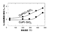
- FIG. 1 is a graph showing the results of analyzing the crystal structure by applying the in-plain X-ray diffraction method.
- FIG. 1 is the substrate temperature (° C.) just before film formation, and the vertical axis of the graph shown in FIG. 1 is the ratio of the fcc crystal structure existing in the CoPt-based alloy particles (magnetic crystal grains). P fcc (%).
- the ratio P fcc of the fcc crystal structure existing in the CoPt alloy particles (magnetic crystal grains) can be reduced, and the ratio of stacking faults It was found that can be reduced.
- FIG. 2 is a graph showing the results of measuring the magnetocrystalline anisotropy constant Ku using a torque magnetometer.
- the horizontal axis of the graph shown in FIG. 2 is the substrate temperature (° C.) just before film formation, and the vertical axis of the graph shown in FIG. 2 is the magnetocrystalline anisotropy constant Ku ( ⁇ 10 6 erg / cm 3 ). .
- the magnetocrystalline anisotropy constant Ku is approximately constant at about 5.4 ⁇ 10 6 erg / cm 3 until the substrate temperature is 200 ° C.
- the magnetocrystalline anisotropy constant Ku monotonously decreases as the substrate temperature increases.
- the magnetocrystalline anisotropy constant Ku is about 1.7 erg / cm 3 .
- the magnetocrystalline anisotropy constant Ku is substantially constant at about 6.5 erg / cm 3 until the substrate temperature is about 300 ° C., and the substrate temperature is 300
- the magnetocrystalline anisotropy constant Ku starts to decrease as the substrate temperature increases from above about 0 ° C.
- the magnetocrystalline anisotropy constant Ku is about 2.5 erg / cm 3 even when the substrate temperature is 470 ° C. there were.
- the crystal magnetic anisotropy constant Ku of the magnetic thin film can be increased by not containing Cr in the CoPt alloy-SiO 2 magnetic thin film.
- the fcc crystal structure existing in the CoPt alloy particles is obtained. This is thought to be due to the fact that the ratio P fcc is reduced and stacking faults are reduced.
- Example 1 The composition of the whole target produced as Example 1 is 91.4 (80Co-20Pt) -8.6WO 3 in terms of molar ratio.
- the target was produced and evaluated as follows. In addition, when the content ratio of the oxide (WO 3 ) is expressed as a volume fraction with respect to the entire target and the composition of the entire target manufactured in Example 1 is expressed, it is (80Co-20Pt) -30 vol% WO 3 .
- the target produced in Example 1 is included in the scope of the target according to the present invention.
- 80Co-20Pt alloy atomized powder was first prepared. Specifically, each metal is weighed so that the alloy composition is Co: 80 at% and Pt: 20 at%, heated to 1500 ° C. or higher to form a molten alloy, and gas atomized to produce 80Co-20Pt alloy atomized powder. did.
- the produced 80Co-20Pt alloy atomized powder was classified with a 150 mesh sieve to obtain an 80Co-20Pt alloy atomized powder having a particle size of 106 ⁇ m or less.
- WO 3 powder 154.44 g was added to 610.00 g of 80Co-20Pt alloy atomized powder after classification, and mixed and dispersed by a ball mill to obtain a mixed powder for pressure sintering.
- the total number of rotations of the ball mill was 1,870,560.
- FIG. 3 and 4 are metallographic micrographs of a cross section in the thickness direction of the obtained sintered body test piece, and FIG. 3 is a photograph with a magnification of 100 times at the time of photographing (scale scale in the photograph is 500 ⁇ m), FIG. 4 is a photograph with a magnification of 500 times at the time of photographing (scale scale in the photograph is 100 ⁇ m).
- the 80Co-20Pt alloy phase and the WO 3 phase were finely mixed and dispersed.
- the layer structure of this magnetic property measurement sample is glass / Ta (5 nm, 0.6 Pa) / Pt (6 nm, 0.6 Pa) / Ru (10 nm, 0.6 Pa) / Ru (10 nm, 8 Pa) / Co 60 Cr 40 ⁇ 26 vol. .% SiO 2 (2 nm, 4 Pa) / CoPt alloy—WO 3 (16 nm, 8 Pa).
- the numbers on the left in parentheses indicate the film thickness, and the numbers on the right indicate the pressure in the Ar atmosphere when sputtering is performed.
- a CoPt alloy-WO 3 is a magnetic thin film formed using the target prepared in Example 1. Note that when the magnetic thin film was formed, the substrate was not heated, but was formed at room temperature.
- the obtained sample for measuring magnetic properties was put into an annealing furnace (vacuum degree 5 ⁇ 10 ⁇ 4 or less) and annealed. Both the temperature increase rate and the temperature decrease rate of the annealing furnace were constant at 200 ° C./h.
- the annealing temperature was 200 ° C., 300 ° C., 400 ° C., 450 ° C., 500 ° C., 600 ° C., and different magnetic property measurement samples were used for each annealing temperature. There are six samples for each annealing temperature, for a total of six samples. In the annealing treatment, the temperature was lowered to room temperature after maintaining 0 h at the annealing temperature. That is, the heating was terminated when the predetermined annealing temperature was reached, and the temperature was lowered to room temperature.
- Samples for measuring magnetic properties (total 6 samples) that were annealed by heating to the target annealing temperature and lowered to room temperature, and samples for measuring magnetic properties that were not annealed after film formation at room temperature (1 MH loops (magnetization curves) were measured using a magneto-optic Kerr effect apparatus. Then, the coercive force Hc was read from each MH loop (magnetization curve).
- the measurement results for the coercive force Hc are shown in FIG. 5 together with the results of other examples and comparative examples.
- the horizontal axis in FIG. 5 is the annealing temperature (° C.), and the vertical axis is the coercive force Hc (kOe).
- Example 1 the coercive force Hc of the sample that was not annealed was 7.1 kOe. This coercive force is equal to or greater than the coercive force of the magnetic thin film realized at the current technical level, and the magnetic thin film of Example 1 can be used as a current perpendicular magnetic recording medium without annealing. The coercive force when used is sufficient.
- Example 1 the coercive force Hc was further increased by annealing. As can be seen from FIG. 5, the coercive force Hc was highest when the annealing temperature was 500.degree. The value was 10.8 kOe, which exceeded 10 kOe. As described above, the coercive force Hc of the magnetic thin film realized at the current technical level is about 6 to 7 kOe, and within the range recognized by the present inventor, the magnetic thin film having a coercive force Hc exceeding 10 kOe. There is no reported example, and this is the first example of a magnetic thin film having a coercive force Hc exceeding 10 kOe in the magnetic thin film of Example 1 (annealed at 500 ° C.).
- the MH loop (magnetization curve) when the largest coercive force Hc is obtained (when the annealing temperature is 500 ° C.) is shown in FIG. 6 together with the results of other examples and comparative examples.
- the horizontal axis in FIG. 6 represents the strength of the applied magnetic field.
- the vertical axis in FIG. 6 is a value normalized by dividing the rotation angle (Kerr rotation angle) of the polarization axis of incident light by the saturation Kerr rotation angle.
- Example 2 The composition of the entire target manufactured as Example 2 is (80Co-20Pt) -30 vol% TiO 2 .
- a target was produced in the same manner as in Example 1 except that the oxide used was TiO 2 .
- the target produced in Example 2 is included in the scope of the target according to the present invention.
- a sample for measuring magnetic properties was produced in the same manner as in Example 1 using the produced target.
- each sample for measuring magnetic properties annealed at target annealing temperatures (200 ° C., 300 ° C., 400 ° C., 450 ° C., 500 ° C., 600 ° C.) and cooled to room temperature ( MH loops (magnetization curves) were measured using a magneto-optic Kerr effect device for each of the samples for magnetic property measurement (one) that had not been annealed after film formation at room temperature. Then, the coercive force Hc was read from each MH loop (magnetization curve).
- Example 2 the coercive force Hc of the sample that was not annealed was 5.8 kOe. However, when annealed, the coercive force Hc was highest when the annealing temperature was 500 ° C. Was 8.6 kOe. As described above, the coercive force Hc of the magnetic thin film realized at the current technical level is about 6 to 7 kOe, and the coercive force Hc of the magnetic thin film of Example 2 (annealed at 500 ° C.) is the current coercive force Hc. It exceeds the coercivity Hc of the magnetic thin film realized at the technical level.
- the MH loop (magnetization curve) when the largest coercive force Hc is obtained (when the annealing temperature is 500 ° C.) is shown in FIG. 6 together with the results of other examples and comparative examples.
- Comparative Example 1 The composition of the entire target manufactured as Comparative Example 1 is (80Co-20Pt) -30 vol% SiO 2 .
- a target was produced in the same manner as in Example 1 except that the oxide used was SiO 2 .
- the oxide used for the target produced in this Comparative Example 1 is SiO 2 and is not included in the scope of the target according to the present invention.
- a sample for measuring magnetic properties was produced in the same manner as in Example 1 using the produced target.
- each sample for measuring magnetic properties annealed at target annealing temperatures (200 ° C., 300 ° C., 400 ° C., 450 ° C., 500 ° C., 600 ° C.) and cooled to room temperature ( MH loops (magnetization curves) were measured using a magneto-optic Kerr effect device for each of the samples for magnetic property measurement (one) that had not been annealed after film formation at room temperature. Then, the coercive force Hc was read from each MH loop (magnetization curve).
- the coercive force Hc of the sample that was not annealed was 5.2 kOe.
- the coercive force Hc was the highest when the annealing temperature was 300 ° C., and its value was 5.5 kOe.
- the MH loop (magnetization curve) when the largest coercive force Hc is obtained (when the annealing temperature is 300 ° C.) is shown in FIG. 6 together with the results of other examples and comparative examples.
- Comparative Example 2 The composition of the entire target manufactured as Comparative Example 2 is (80Co-20Pt) -30 vol% Al 2 O 3 .
- a target was produced in the same manner as in Example 1 except that the oxide used was Al 2 O 3 .
- the oxide used for the target produced in this Comparative Example 2 is Al 2 O 3 and is not included in the range of the target according to the present invention.
- a sample for measuring magnetic properties was produced in the same manner as in Example 1 using the produced target.
- each sample for measuring magnetic properties annealed at target annealing temperatures (200 ° C., 300 ° C., 400 ° C., 450 ° C., 500 ° C., 600 ° C.) and cooled to room temperature ( MH loops (magnetization curves) were measured using a magneto-optic Kerr effect device for each of the samples for magnetic property measurement (one) that had not been annealed after film formation at room temperature. Then, the coercive force Hc was read from each MH loop (magnetization curve).
- the coercive force Hc of the sample that was not annealed was 0.9 kOe.
- the coercive force Hc was the highest when the annealing temperature was 600 ° C., and the value was 2.3 kOe.
- the MH loop (magnetization curve) when the largest coercive force Hc is obtained (when the annealing temperature is 600 ° C.) is shown in FIG. 6 together with the results of other examples and comparative examples.
- Example 1 (Discussion about oxides)
- the oxide used in Example 1 is WO 3
- the oxide used in Example 2 is TiO 2
- the oxide used in Comparative Example 1 is SiO 2
- the oxide used in Comparative Example 2 Is Al 2 O 3 .
- the nucleation magnetic field Hn (kOe) and the slope ⁇ of the MH loop (magnetization curve) were further calculated.
- the slope ⁇ of the MH loop (magnetization curve) was calculated by the calculation formula 4 ⁇ ⁇
- the calculation results of the nucleation magnetic field Hn (kOe) and the slope ⁇ of the MH loop are shown together in the following Table 1 together with the maximum value of the coercive force Hc described above.
- the values of coercive force Hc and nucleation magnetic field Hn of the magnetic thin film are greatest in Example 1 using WO 3 as the oxide, and the values are 10.8 (kOe) and 5. 5 (kOe).
- the coercive force Hc of the magnetic thin film realized at the current technical level is about 6 to 7 kOe, and within the range recognized by the present inventor, the magnetic thin film having a coercive force Hc exceeding 10 kOe.
- the magnetic thin film of Example 1 (annealed at 500 ° C.) is the first example of a magnetic thin film having a coercive force Hc exceeding 10 kOe.
- the magnetic thin film of Example 1 using WO 3 as an oxide (after annealing at 500 ° C.) has a small MH loop slope ⁇ of 1.6, and magnetization reversal does not occur abruptly. Very Hard to think.
- the magnetic thin film of Example 1 (annealed at 500 ° C.) using WO 3 as an oxide has a large coercive force Hc and nucleation magnetic field Hn, and a small MH loop slope ⁇ , so that the magnetic recording film It is considered that the thermal stability of the recording signal when used as is extremely good.
- the magnetic thin film of Example 1 using WO 3 as the oxide has a higher coercive force Hc as the annealing temperature is increased in the annealing temperature range of 500 ° C. or lower. It is also a magnetic thin film having a characteristic that the coercive force Hc is improved by annealing at 500 ° C. or lower.
- the magnetic thin film of Example 1 using WO 3 as the oxide has a coercive force Hc of 7.1 kOe even in a state where the annealing process is not performed (a state where the film is formed at room temperature).
- the coercive force is equal to or higher than that of the magnetic thin film realized at the current technical level. Therefore, the magnetic thin film of Example 1 has a sufficient coercive force as a coercive force when used as a current perpendicular magnetic recording medium, even without annealing.
- coercive force Hc and nucleation magnetic field Hn of the magnetic thin film of Example 2 are 8.6 (kOe) and 4.9 (kOe), respectively.
- it is lower than the value of the magnetic thin film of Example 1, it is a magnetic thin film exceeding the coercive force realized when compared with the current magnetic thin film, and the thermal stability of the recording signal when used as a magnetic recording film is good It is thought that it becomes.
- the magnetic thin film of Example 2 using TiO 2 as an oxide has a higher coercive force Hc as the annealing temperature is increased within the annealing temperature range of 500 ° C. or lower. It is also a magnetic thin film having a characteristic that the coercive force Hc is improved by annealing at 500 ° C. or lower.
- the magnetic thin film of Comparative Example 1 using SiO 2 as the oxide and the magnetic thin film of Comparative Example 2 using Al 2 O 3 as the oxide have the same coercive force regardless of whether annealing is performed.
- the coercive force (6 to 7 kOe) of the magnetic thin film realized at the technical level has not been reached, and it is considered that the thermal stability of the recording signal when used as a magnetic recording film cannot be improved.
- FIG. 7 shows a TEM photograph of the magnetic thin film of Example 1.
- FIG. 7 (a) is a planar TEM photograph (TEM photograph of a plane in the plane direction of the magnetic thin film) of the CoPt—WO 3 magnetic thin film that has not been annealed, and FIG. 7 (b) is annealed at 500 ° C. 4 is a planar TEM photograph of a CoPt—WO 3 magnetic thin film subjected to the treatment.
- the dark gray region is a CoPt alloy
- the white region is WO 3 .
- the CoPt alloy magnetic crystal grains are separated by about 1 nm by WO 3 regardless of the presence or absence of annealing treatment, and have a good granular structure.
- each CoPt alloy magnetic crystal grain area is obtained using a planar TEM photograph at 100 or more locations, and the crystal grain diameter (diameter of the cylinder) is assumed when the CoPt alloy magnetic crystal grain shape is assumed to be a cylinder.
- the thickness was 6.4 nm when the annealing treatment was not performed, and the thickness was 8 nm when the annealing treatment was performed at 500 ° C. From this, it is considered that the CoPt alloy magnetic crystal grains grow in a columnar shape by the annealing treatment.
- FIG. 7C is a cross-sectional TEM photograph (TEM photograph of a cross section in a direction perpendicular to the plane of the magnetic thin film) of the CoPt—WO 3 magnetic thin film annealed at 500 ° C.
- TEM photograph of a cross section in a direction perpendicular to the plane of the magnetic thin film As can be seen from this cross-sectional TEM photograph, in the CoPt—WO 3 magnetic thin film annealed at 500 ° C., it can be seen that the CoPt alloy magnetic crystal grains grow in a columnar shape.
- CoPt—WO 3 magnetic thin film had a good granular structure regardless of the annealing treatment. It was also confirmed that CoPt alloy magnetic crystal grains can be grown in a columnar shape by annealing the CoPt—WO 3 magnetic thin film at 500 ° C.
- FIG. 5 graph showing the relationship between the annealing temperature and the coercive force Hc for a suitable annealing temperature for the magnetic thin films of Examples 1 and 2 ).
- the annealing temperature when the annealing temperature is in the temperature range of 300 ° C. or more and 550 ° C. or less, the coercive force Hc of the magnetic thin films of Examples 1 and 2 is about 6.5 kOe or more, which is the current technical level. It becomes a value equal to or greater than the coercive force Hc of the magnetic thin film. Therefore, the annealing temperature for the magnetic thin films of Examples 1 and 2 is preferably in the temperature range of 300 ° C. or higher and 550 ° C. or lower.
- the coercive force Hc of the magnetic thin film of Example 1 is about 9 kOe or more, which exceeds the current technical level. Coercive force Hc is expressed. Also, the coercive force Hc of the magnetic thin film of Example 2 is about 7.1 kOe or higher when the annealing temperature is in the temperature range of 400 ° C. or higher and 520 ° C. or lower, compared with the magnetic thin film of the current technical level. A coercive force Hc equal to or higher than that is obtained. Therefore, the annealing temperature for the magnetic thin films of Examples 1 and 2 is more preferably in the temperature range of 400 ° C. or more and 520 ° C. or less.
- the coercive force Hc of the magnetic thin film of Example 1 is about 10 kOe or more.
- the coercive force Hc which has not been reached in the thin film, is expressed.
- the coercive force Hc of the magnetic thin film of Example 2 is about 8 kOe or more when the annealing temperature is in a temperature range of 460 ° C. or more and 520 ° C. or less, and a coercive force Hc exceeding the current technical level is obtained. ing. Therefore, the annealing temperature for the magnetic thin films of Examples 1 and 2 is more preferably in the temperature range of 460 ° C. or more and 520 ° C. or less.
- the annealing temperature for the magnetic thin films of Examples 1 and 2 is particularly preferably in the temperature range of 480 ° C. or more and 510 ° C. or less.
- the magnetic magnetic anisotropy constant K u grain and the anisotropic magnetic field H k grain are excluded from the value of the average magnetic property of the CoPt—WO 3 magnetic thin film by excluding the influence by 30 vol% of WO 3 by calculation. Was calculated.
- K u grain (M s grain ⁇ H k grain ) / 2 between the magnetocrystalline anisotropy constant K u grain and the anisotropic magnetic field H k grain .
- M s grain is the saturation magnetization of each crystal grain, and was calculated from the value of the average saturation magnetization measured with a sample vibration magnetometer.
- the saturation magnetization M s grain of each crystal grain was a substantially constant value regardless of the presence or absence of annealing treatment and the annealing temperature, and was about 990 emu / cm 3 .
- FIG. 8 is a graph showing the magnetocrystalline anisotropy constant K u grain and the anisotropic magnetic field H k grain calculated for the CoPt alloy magnetic crystal grains in the magnetic thin film of Example 1.
- the horizontal axis of the graph shown in FIG. 8 is the annealing temperature (° C.), and the vertical axis is the magnetocrystalline anisotropy constant K u grain ( ⁇ 10 6 erg / cm 3 ) and the anisotropic magnetic field H k grain (kOe). is there.
- the magnetocrystalline anisotropy constant K u grain is from 7.8 ⁇ 10 6 erg / cm 3 to 10.4 ⁇ 10 6 erg / cm 3.
- the anisotropic magnetic field H k grain increases from 15.7 kOe to 21 kOe.
- the change in the magnetocrystalline anisotropy constant K u grain and the anisotropic magnetic field H k grain is similar to the change in the coercive force Hc shown in FIG. It believed to be based on the increase in the crystal magnetic anisotropy constant K u grain.
- composition of Co and Pt in the sputtering target used in Examples 1 and 2 and Comparative Examples 1 and 2 is only one type of 80Co-20Pt.
- the magnetic thin film produced without heating the substrate was annealed at 500 ° C. using a sputtering target (the oxide contains 30 vol% of WO 3 ) with different compositions of Co and Pt.
- the coercive force Hc and nucleation magnetic field Hn of the magnetic thin film were measured, and the composition range of Co and Pt in the sputtering target in which the effect of the present invention was manifested was examined.
- compositions of Co and Pt in the additionally studied sputtering targets were 90Co-10Pt in Example 3, 85Co-15Pt in Example 4, and Example 5 Is 50Co-50Pt, Example 6 is 25Co-75Pt, and Example 7 is 20Co-80Pt.
- the metal component in the sputtering target of the comparative example 3 is only Co
- the metal component in the sputtering target of the comparative example 4 is only Pt.
- a target was prepared in the same manner as in Example 1 except that the composition of Co and Pt was changed, and the coercive force Hc and nucleation magnetic field Hn of the magnetic thin film were measured in the same manner as in Example 1. The measurement results are shown in the following Table 2 together with the measurement results of Example 1.
- the coercive force Hc after annealing at 500 ° C. of the magnetic thin film produced using the sputtering target (Example 1, Examples 3 to 7) within the scope of the present invention is 6.8 kOe or more.
- the coercive force was equal to or greater than the coercive force of the current technical level.
- Examples 1, 5, and 6 had a coercive force of 10 kOe or more, and an extremely large coercive force was obtained.
- the sputtering target of Comparative Example 3 in which the metal component in the sputtering target is only Co and is outside the scope of the present invention and the Comparative Example 4 in which the metal component in the sputtering target is only Pt and is outside the scope of the present invention.
- the coercivity Hc after annealing at 500 ° C. of the magnetic thin film produced using the sputtering target was as small as 0.5 kOe and 0.0 kOe, respectively.
- the coercive force Hc after annealing at 500 ° C. of the magnetic thin film produced using the sputtering target (Example 1, Examples 3 to 7) within the scope of the present invention is 6.8 kOe or more. Compared with the coercive force of the current technical level, the coercive force is more than equivalent, and good results were obtained.
- the magnetic thin film produced without heating the substrate was annealed at 500 ° C. using a sputtering target (Co and Pt composition was 80Co-20Pt) with different contents of WO 3 , and the annealing treatment was performed.
- the coercive force Hc and the nucleation magnetic field Hn of the magnetic thin film were measured, and the range of the content of WO 3 in the sputtering target in which the effect of the present invention was exhibited was examined.
- Example 8 to 13 and Comparative Example 5 The content of WO 3 in the additionally studied sputtering targets (Examples 8 to 13 and Comparative Example 5) is 10 vol% in Example 8, 20 vol% in Example 9, and 25 vol% in Example 10. Yes, Example 11 is 35 vol%, Example 12 is 40 vol%, Example 13 is 50 vol%, and Comparative Example 5 is 0 vol%.
- a target was prepared in the same manner as in Example 1 except that the content of WO 3 was changed, and the coercive force Hc and nucleation magnetic field Hn of the magnetic thin film were measured in the same manner as in Example 1. The measurement results are shown in the following Table 3 together with the measurement results of Example 1.
- the coercive force Hc after annealing at 500 ° C. of the magnetic thin film produced using the sputtering target (Example 1, Examples 8 to 13) within the scope of the present invention is 6.9 kOe or more.
- the coercive force was equal to or greater than the coercive force of the current technical level.
- Examples 1, 10, 11, and 12 had a coercive force of 10 kOe or more, and an extremely large coercive force was obtained.
- the coercive force Hc after annealing at 500 ° C. of the magnetic thin film produced using the sputtering target of Comparative Example 5 having a WO 3 content of 0 and outside the scope of the present invention was as small as 0.7 kOe.
Landscapes
- Chemical & Material Sciences (AREA)
- Engineering & Computer Science (AREA)
- Organic Chemistry (AREA)
- Materials Engineering (AREA)
- Mechanical Engineering (AREA)
- Metallurgy (AREA)
- Physics & Mathematics (AREA)
- Chemical Kinetics & Catalysis (AREA)
- Thermal Sciences (AREA)
- Crystallography & Structural Chemistry (AREA)
- Ceramic Engineering (AREA)
- Plasma & Fusion (AREA)
- Analytical Chemistry (AREA)
- Manufacturing & Machinery (AREA)
- Structural Engineering (AREA)
- Physical Vapour Deposition (AREA)
- Manufacturing Of Magnetic Record Carriers (AREA)
- Compositions Of Oxide Ceramics (AREA)
- Powder Metallurgy (AREA)
Abstract
保磁力Hcの大きい磁性薄膜を作製可能なスパッタリングターゲットおよびその製造方法を提供する。 金属Co、金属Pt、および酸化物を含有してなるスパッタリングターゲットであって、金属Crを含有せず、かつ、前記酸化物は、WO3およびTiO2のうちの少なくともいずれか一方を有してなる。
Description
本発明はスパッタリングターゲットおよびその製造方法に関し、詳しくは、保磁力の大きい磁性薄膜を作製可能なスパッタリングターゲットおよびその製造方法に関する。なお、以下において、スパッタリングターゲットを単に「ターゲット」と記すことがある。
ハードディスクドライブの磁気ディスクにおいて、情報信号の記録を担う磁気記録膜として、CoPtCr-酸化物系のグラニュラ構造からなる磁性薄膜が用いられている(例えば、非特許文献1参照。)。この磁性薄膜において記録密度をさらに向上させるためには、磁気記録層(磁性薄膜)に含まれる磁性結晶粒子を微細化する必要がある。
ところが、磁性結晶粒子の微細化が進展した結果、超常磁性現象により記録信号の熱安定性が損なわれて記録信号が消失してしまうという、いわゆる熱揺らぎ現象が発生するようになった。この熱揺らぎ現象は、磁気ディスクの高記録密度化への大きな障害となっている。
この障害を解決するためには、各磁性結晶粒子において、磁気エネルギーが熱エネルギーに打ち勝つように磁気エネルギーを増大させることが必要であるが、各磁性結晶粒子の磁気エネルギーは磁性結晶粒子の体積vと結晶磁気異方性定数Kuとの積v×Kuで決定される。このため、磁気エネルギーを増大させるためには磁性結晶粒子の結晶磁気異方性定数Kuを増大させることが必要不可欠である(例えば、非特許文献2参照。)。
現行の垂直磁気記録膜の構造は、柱状のCoPtCr結晶粒とその周囲を取り囲む酸化物の結晶粒界とからなるグラニュラ構造となっている。このグラニュラ構造からなるCoPtCr-酸化物膜の結晶磁気異方性定数Kuを大きくするために、基板温度を昇温させた状態でスパッタリングを行うことが試みられている。基板温度を昇温させた状態でスパッタリングを行うことにより、成膜中に金属原子(Co原子、Pt原子、Cr原子)の拡散を促進させて、良好な磁性結晶粒を得ようとする試みである。
しかしながら、基板温度を昇温させた状態でスパッタリングを行って、CoPtCr-酸化物膜を作製すると、CoPtCr磁性結晶粒が柱状ではなく球状に成長してしまい、磁性結晶粒の磁気異方性が低下して、得られたCoPtCr-酸化物膜の結晶磁気異方性定数Kuが低下してしまうという現象が生じてしまっていた(非特許文献3参照。)。
そこで、本発明者らは、基板を昇温させていない状態で(室温で)CoPtCr-酸化物膜を作製し、その後にアニールをすることにより結晶磁気異方性定数Kuを向上させることを試みた。しかし、アニールをすると、柱状のCoPtCr磁性結晶粒の下方部(基板に近い側の部位)の径が大きくなってしまって、CoPtCr磁性結晶粒の下方部で磁気的な結合が生じ、粒間相互作用が大きくなってしまい、逆に保磁力Hcが低下してしまった。
T. Oikawa et al., IEEE TRANSACTIONS ON MAGNETICS, 2002年9月, VOL.38, NO.5, p.1976-1978
S. N. Piramanayagam, JOURNAL OF APPLIED PHYSICS, 2007年, 102, 011301
日向慎太郎、外4名、第37回 日本磁気学会学術講演会、2013年9月、5aA-1
本発明は、かかる状況に鑑みてなされたものであって、保磁力Hcの大きい磁性薄膜を作製可能なスパッタリングターゲットおよびその製造方法を提供することを第1の課題とする。
また、アニール処理をすることにより保磁力Hcを大きくすることができる磁性薄膜を作製可能なスパッタリングターゲットおよびその製造方法を提供することを第2の課題とする。
本発明者は、前記課題を解決するべく鋭意研究した結果、グラニュラ構造の磁性薄膜(垂直磁気記録膜)中の磁性結晶粒を、現状の磁性薄膜(垂直磁気記録膜)で用いられているCoPtCr合金で形成するのではなく、Crを用いないCoPt合金で形成することにより、結晶磁気異方性定数Kuを向上させることができることを見出した。
さらに、本発明者は、磁性結晶粒をCoPt合金で形成してCoPt-酸化物膜を作製する場合に用いる酸化物としては、室温で成膜して得られる膜の保磁力Hcが大きい点および室温で成膜して得られる膜をアニール処理することによりさらに保磁力Hcを大きくできる点で、WO3およびTiO2が良好であり、その中でも特にWO3が良好であることを見出した。
本発明は、これらの新たな知見に基づきなされたものである。
即ち、本発明に係るスパッタリングターゲットは、金属Co、金属Pt、および酸化物を含有してなるスパッタリングターゲットであって、金属Crを含有せず、かつ、前記酸化物は、WO3およびTiO2のうちの少なくともいずれか一方を有してなることを特徴とするスパッタリングターゲットである。
前記スパッタリングターゲットにおいて、金属Coと金属Ptの合計に対して金属Coを20~90at%含有することが好ましい。
前記酸化物は、WO3およびTiO2のうちの少なくともいずれか一方であることが好ましい。
また、前記酸化物は、WO3を有してなることが好ましい。
また、前記酸化物は、WO3であることが好ましい。
また、前記酸化物を10~50vol%含有することが好ましく、前記酸化物を25~35vol%含有することがより好ましい。
また、前記スパッタリングターゲットは、磁性薄膜の作製に使用可能であることが好ましい。
前記スパッタリングターゲットを用いて作製された磁性薄膜に対して300℃以上550℃以下の温度範囲でアニール処理を行うことにより、該磁性薄膜の保磁力を、現状の技術レベルにおいて実現されている保磁力(以下、「現状の技術水準の保磁力」と記すことがある。)と比べて同等以上の保磁力である6kOe以上にできることが好ましい。
前記酸化物はWO3を有してなり、前記スパッタリングターゲットを用いて作製された磁性薄膜に対して400℃以上520℃以下の温度範囲でアニール処理を行うことにより、該磁性薄膜の保磁力を、現状の技術水準の保磁力を上回る9kOe以上にできることがより好ましい。
また、前記酸化物はWO3を有してなり、前記スパッタリングターゲットを用いて作製された磁性薄膜に対して460℃以上520℃以下の温度範囲でアニール処理を行うことにより、該磁性薄膜の保磁力を、現状の技術水準の保磁力を上回る10kOe以上にできることがさらに好ましい。
前記アニール処理を行った後の前記磁性薄膜の構造がグラニュラ構造であることが好ましい。
本発明に係るスパッタリングターゲットの製造方法の第1の態様は、CoおよびPtを含有する一方Crを含有しないCoPt合金粉末をアトマイズ法で作製する工程と、前記作製したCoPt合金粉末と、酸化物粉末とを混合分散して加圧焼結用混合粉末を作製する工程と、前記作製した加圧焼結用混合粉末を加圧焼結する工程と、を有し、前記酸化物粉末は、WO3およびTiO2のうちの少なくともいずれか一方を有してなることを特徴とするスパッタリングターゲットの製造方法である。
本発明に係るスパッタリングターゲットの製造方法の第2の態様は、Co粉末と、Pt粉末と、酸化物粉末とを混合分散して加圧焼結用混合粉末を得る工程と、前記得られた加圧焼結用混合粉末を加圧焼結する工程と、を有し、前記酸化物粉末は、WO3およびTiO2のうちの少なくともいずれか一方を有してなることを特徴とするスパッタリングターゲットの製造方法である。
前記製造方法によって得られるスパッタリングターゲットは、金属Coと金属Ptの合計に対して金属Coを20~90at%含有することが好ましい。
前記酸化物粉末は、WO3およびTiO2のうちの少なくともいずれか一方であることが好ましい。
また、前記酸化物粉末は、WO3を有してなることが好ましい。
また、前記酸化物粉末は、WO3であることが好ましい。
また、前記酸化物粉末の前記加圧焼結用混合粉末の全体に対する体積分率が10~50vol%であることが好ましく、25~35vol%であることがより好ましい。
本発明によれば、保磁力Hcの大きい磁性薄膜を作製可能なスパッタリングターゲットおよびその製造方法を提供することができる。
また、アニール処理をすることにより保磁力Hcを大きくすることができる磁性薄膜を作製可能なスパッタリングターゲットおよびその製造方法を提供することができる。
本発明の実施形態に係るスパッタリングターゲットは、金属Co、金属Pt、および酸化物を含有してなるスパッタリングターゲットであって、金属Crを含有せず、かつ、前記酸化物は、WO3およびTiO2のうちの少なくともいずれか一方を有してなることを特徴とする。
1.ターゲットの構成成分
本実施形態に係るスパッタリングターゲットは、金属成分としてCoおよびPtを含むが、磁性薄膜を形成する支障とならなければさらに他の金属(例えば、Au、Ag、Ru、Rh、Pd、Ir、W、Ta、Cu、B、Mo等)を含んでいてもよい。ただし、後述する参考例で実証しているように、金属Crが含まれていると磁性薄膜の結晶磁気異方性定数Kuに悪影響を与えるので、金属Crを含めることはできない。
本実施形態に係るスパッタリングターゲットは、金属成分としてCoおよびPtを含むが、磁性薄膜を形成する支障とならなければさらに他の金属(例えば、Au、Ag、Ru、Rh、Pd、Ir、W、Ta、Cu、B、Mo等)を含んでいてもよい。ただし、後述する参考例で実証しているように、金属Crが含まれていると磁性薄膜の結晶磁気異方性定数Kuに悪影響を与えるので、金属Crを含めることはできない。
金属Coおよび金属Ptは、スパッタリングによって形成される磁性薄膜のグラニュラ構造において、磁性結晶粒(微小な磁石)の構成成分となる。
Coは強磁性金属元素であり、磁性薄膜のグラニュラ構造の磁性結晶粒(微小な磁石)の形成において中心的な役割を果たす。スパッタリングによって得られる磁性薄膜中のCoPt合金粒子(磁性結晶粒)の結晶磁気異方性定数を大きくするという観点および得られる磁性薄膜中のCoPt合金粒子の磁性を維持するという観点から、本実施形態に係るスパッタリングターゲット中の金属Coの含有割合は、金属成分の全体(金属Coと金属Ptの合計)に対して20~90at%とすることが好ましく、25~85at%とすることがより好ましい。
Ptは、所定の組成範囲でCoと合金化することにより合金の磁気モーメントを低減させる機能を有し、磁性結晶粒の磁性の強さを調整する役割を有する。スパッタリングによって得られる磁性薄膜中のCoPt合金粒子(磁性結晶粒)の結晶磁気異方性定数を大きくするという観点および得られる磁性薄膜中のCoPt合金粒子(磁性結晶粒)の磁性を調整するという観点から、本実施形態に係るスパッタリングターゲット中の金属Ptの含有割合は、金属成分の全体に対して10~80at%とすることが好ましく、15~75at%とすることがより好ましい。
また、本実施形態に係るスパッタリングターゲットは、酸化物成分としてWO3およびTiO2のうちの少なくともいずれか一方を含む。酸化物成分は、磁性薄膜のグラニュラ構造において、磁性結晶粒(微小な磁石)同士の間を仕切る非磁性マトリックスとなる。
本実施形態に係るスパッタリングターゲットは、酸化物としてWO3およびTiO2のうちの少なくともいずれか一方を含むが、磁性薄膜を形成する支障とならなければさらに他の酸化物(例えば、SiO2、Ti2O3、Ta2O5、Cr2O3、CoO、Co3O4、B2O3、Fe2O3、CuO、Y2O3、MgO、Al2O3、ZrO2、Nb2O5、MoO3、CeO2、Sm2O3、Gd2O3、WO2、HfO2、NiO2等)を含んでいてもよい。ただし、後述する実施例で実証しているように、酸化物としてWO3またはTiO2を用いることにより、室温で成膜して得られる磁性薄膜の保磁力Hcを大きくできるとともに、室温で成膜して得られる磁性薄膜をアニール処理することによりさらに保磁力Hcを大きくできるので、酸化物としてはWO3またはTiO2を用いることが好ましい。また、後述する実施例で実証しているように、WO3を用いることにより、作製する磁性薄膜の保磁力Hcを特に大きくすることができるので、酸化物としてはWO3を用いることが特に好ましい。
スパッタリングターゲット全体に対する金属成分の含有割合および酸化物成分の含有割合は、目的とする磁性薄膜の成分組成によって決まり、特に限定されているわけではないが、スパッタリングターゲット全体に対する金属成分の含有割合は例えば88~94mol%とすることができ、スパッタリングターゲット全体に対する酸化物成分の含有割合は例えば6~12mol%とすることができる。
酸化物成分は、前述したように、磁性薄膜のグラニュラ構造において、磁性結晶粒(微小な磁石)同士の間を仕切る非磁性マトリックスとなる。このため、磁性薄膜中の酸化物の含有量を多くした方が磁性結晶粒同士の間を確実に仕切りやすくなり、磁性結晶粒同士を独立させやすくなるので好ましい。この点から、本実施形態に係るスパッタリングターゲット中に含まれる酸化物の含有量は10vol%以上であることが好ましく、20vol%以上であることがより好ましく、25vol%以上であることがさらに好ましい。
ただし、磁性薄膜中の酸化物の含有量が多くなりすぎると、酸化物がCoPt合金粒子(磁性結晶粒)中に混入してCoPt合金粒子(磁性結晶粒)の結晶性に悪影響を与えて、CoPt合金粒子(磁性結晶粒)においてhcp以外の構造の割合が増えるおそれがある。また、磁性薄膜における単位面積あたりの磁性結晶粒の数が減るため、記録密度を高めにくくなる。これらの点から、本実施形態に係るスパッタリングターゲット中に含まれる酸化物の含有量は50vol%以下であることが好ましく、40vol%以下であることがより好ましく、35vol%以下であることがさらに好ましい。
したがって、本実施形態に係るスパッタリングターゲット中に含まれる酸化物のスパッタリングターゲット全体に対する含有量は、10~50vol%であることが好ましく、20~40vol%であることがより好ましく、25~35vol%であることがさらに好ましい。
2.スパッタリングターゲットのミクロ構造
本実施形態に係るスパッタリングターゲットのミクロ構造は特に限定されるわけではないが、金属相と酸化物相とが微細に分散し合ってお互いに分散し合ったミクロ構造とすることが好ましい。このようなミクロ構造とすることにより、スパッタリングを実施している際に、ノジュールやパーティクル等の不具合が発生しにくくなる。
本実施形態に係るスパッタリングターゲットのミクロ構造は特に限定されるわけではないが、金属相と酸化物相とが微細に分散し合ってお互いに分散し合ったミクロ構造とすることが好ましい。このようなミクロ構造とすることにより、スパッタリングを実施している際に、ノジュールやパーティクル等の不具合が発生しにくくなる。
3.スパッタリングターゲットの製造方法
本実施形態に係るスパッタリングターゲットは、例えば、以下のようにして製造することができる。ここでは、用いる酸化物をWO3とした場合の製造方法の例について説明する。
本実施形態に係るスパッタリングターゲットは、例えば、以下のようにして製造することができる。ここでは、用いる酸化物をWO3とした場合の製造方法の例について説明する。
(1)CoPt合金アトマイズ粉末の作製
所定の組成(金属Coと金属Ptとの合計に対する該金属Coの原子数比が20~90at%)となるように金属Co、金属Ptを秤量してCoPt合金溶湯を作製する。そして、ガスアトマイズを行い、所定の組成(金属Coと金属Ptとの合計に対する該金属Coの原子数比が20~90at%であることが好ましい。)のCoPt合金アトマイズ粉末を作製する。作製したCoPt合金アトマイズ粉末は分級して、粒径が所定の粒径以下(例えば106μm以下)となるようにする。
所定の組成(金属Coと金属Ptとの合計に対する該金属Coの原子数比が20~90at%)となるように金属Co、金属Ptを秤量してCoPt合金溶湯を作製する。そして、ガスアトマイズを行い、所定の組成(金属Coと金属Ptとの合計に対する該金属Coの原子数比が20~90at%であることが好ましい。)のCoPt合金アトマイズ粉末を作製する。作製したCoPt合金アトマイズ粉末は分級して、粒径が所定の粒径以下(例えば106μm以下)となるようにする。
なお、CoPt合金アトマイズ粉末の磁性を大きくできる点で、含有する金属Coと金属Ptとの合計に対する該金属Coの原子数比を25at%以上とすることがより好ましく、30at%以上とすることがさらに好ましい。
(2)加圧焼結用混合粉末の作製
(1)で作製したCoPt合金アトマイズ粉末にWO3粉末を加えてボールミルで混合分散して、加圧焼結用混合粉末を作製する。CoPt合金アトマイズ粉末とWO3粉末とをボールミルで混合分散することにより、CoPt合金アトマイズ粉末とWO3粉末とが微細に分散した加圧焼結用混合粉末を作製することができる。
(1)で作製したCoPt合金アトマイズ粉末にWO3粉末を加えてボールミルで混合分散して、加圧焼結用混合粉末を作製する。CoPt合金アトマイズ粉末とWO3粉末とをボールミルで混合分散することにより、CoPt合金アトマイズ粉末とWO3粉末とが微細に分散した加圧焼結用混合粉末を作製することができる。
得られるスパッタリングターゲットを用いて作製される磁性薄膜において、WO3によって磁性結晶粒同士の間を確実に仕切って磁性結晶粒同士を独立させやすくなる観点、CoPt合金粒子(磁性結晶粒)がhcp構造となりやすくなる観点、および記録密度を高める観点から、WO3粉末の加圧焼結用混合粉末の全体に対する体積分率は、10~50vol%であることが好ましく、15~40vol%であることがより好ましく、25~35vol%であることがさらに好ましい。
(3)成形
(2)で作製した加圧焼結用混合粉末を、例えば真空ホットプレス法により加圧焼結して成形し、スパッタリングターゲットを作製する。(2)で作製した加圧焼結用混合粉末はボールミルで混合分散されており、CoPt合金アトマイズ粉末とWO3粉末とが微細に分散し合っているので、本製造方法により得られたスパッタリングターゲットを用いてスパッタリングを行っているとき、ノジュールやパーティクルの発生等の不具合は発生しにくい。
(2)で作製した加圧焼結用混合粉末を、例えば真空ホットプレス法により加圧焼結して成形し、スパッタリングターゲットを作製する。(2)で作製した加圧焼結用混合粉末はボールミルで混合分散されており、CoPt合金アトマイズ粉末とWO3粉末とが微細に分散し合っているので、本製造方法により得られたスパッタリングターゲットを用いてスパッタリングを行っているとき、ノジュールやパーティクルの発生等の不具合は発生しにくい。
なお、加圧焼結用混合粉末を加圧焼結する方法は特に限定されず、真空ホットプレス法以外の方法でもよく、例えばHIP法等を用いてもよい。
(4)変形例
(1)~(3)で説明した製造方法の例では、アトマイズ法を用いてCoPt合金アトマイズ粉末を作製し、作製したCoPt合金アトマイズ粉末にWO3粉末を加えてボールミルで混合分散して、加圧焼結用混合粉末を作製しているが、CoPt合金アトマイズ粉末を用いることに替えて、Co単体粉末およびPt単体粉末を用いてもよい。この場合には、Co単体粉末、Pt単体粉末、およびWO3粉末の3種類の粉末をボールミルで混合分散して加圧焼結用混合粉末を作製する。
(1)~(3)で説明した製造方法の例では、アトマイズ法を用いてCoPt合金アトマイズ粉末を作製し、作製したCoPt合金アトマイズ粉末にWO3粉末を加えてボールミルで混合分散して、加圧焼結用混合粉末を作製しているが、CoPt合金アトマイズ粉末を用いることに替えて、Co単体粉末およびPt単体粉末を用いてもよい。この場合には、Co単体粉末、Pt単体粉末、およびWO3粉末の3種類の粉末をボールミルで混合分散して加圧焼結用混合粉末を作製する。
以下では、まず参考例において、本発明に係るスパッタリングターゲットにおいて金属Crを含有させていない根拠となったデータを示す。詳しくは、グラニュラ構造の磁性薄膜中の磁性結晶粒を、現状の垂直磁気記録膜で用いられているCoPtCr合金で形成するのではなく、Crを含有していないCoPt合金で形成することにより、結晶磁気異方性定数Kuが向上する実験結果を示す。この参考例に示す実験結果を踏まえ、本発明では、磁性薄膜の形成に用いるスパッタリングターゲットから金属Crを除いている。
そして、磁性薄膜の形成に用いるスパッタリングターゲットから金属Crを除くこと(磁性薄膜中の磁性結晶粒を、Crを含有していないCoPt合金で形成すること)を前提に、実施例および比較例においては4種類の酸化物で検討を行い、酸化物としてWO3を選択することで、10kOeを超える保磁力Hcを有する磁性薄膜を実現できるスパッタリングターゲットを得るに至った。現状の技術レベルにおいて実現されている磁性薄膜の保磁力Hcは6~7kOe程度であり、本発明者の認識している範囲では、10kOeを超える保磁力Hcを有する磁性薄膜の報告例は現時点において存在しない。
(参考例)
DCスパッタ装置を用いてスパッタリングを行い、磁気記録膜を作製した。磁気記録膜はガラス基板上に作製した。作製した磁気記録膜の層構成は、ガラス基板に近い方から順に表示して、Ta(5nm, 0.6Pa)/Pt(6nm, 0.6Pa)/Ru(10nm, 0.6Pa)/Ru(10nm, 8Pa)/Co60Cr40-26vol.%SiO2(2nm, 4Pa)/CoPt系合金-SiO2(16nm, 4Pa)/C (7nm, 0.6Pa)である。括弧内の左側の数字は膜厚を示し、右側の数字はスパッタリングを行ったときのAr雰囲気の圧力を示す。
DCスパッタ装置を用いてスパッタリングを行い、磁気記録膜を作製した。磁気記録膜はガラス基板上に作製した。作製した磁気記録膜の層構成は、ガラス基板に近い方から順に表示して、Ta(5nm, 0.6Pa)/Pt(6nm, 0.6Pa)/Ru(10nm, 0.6Pa)/Ru(10nm, 8Pa)/Co60Cr40-26vol.%SiO2(2nm, 4Pa)/CoPt系合金-SiO2(16nm, 4Pa)/C (7nm, 0.6Pa)である。括弧内の左側の数字は膜厚を示し、右側の数字はスパッタリングを行ったときのAr雰囲気の圧力を示す。
作製した前記磁気記録膜の層構成において、CoPt系合金-SiO2が垂直磁気記録媒体の記録層となる磁性薄膜である。本参考例では、CoPt系合金-SiO2からなる磁性薄膜における磁性結晶粒を、Crを含むCoPtCr合金で形成したサンプル(磁性薄膜の組成をCo74Pt16Cr10-25vol.%SiO2としたサンプル)と、Crを含まないCoPt合金で形成したサンプル(磁性薄膜の組成をCo82.4Pt17.6-27.7vol.%SiO2としたサンプル)を作製した。したがって、本参考例における前記磁気記録膜の層構成において「CoPt系合金-SiO2」におけるCoPt系合金は、Crを含有する3元系のCoPtCr合金と、Crを含有しない2元系のCoPt合金の両方を意味している。以下においても、CoPt系合金と記載した場合は、Crを含有する3元系のCoPtCr合金と、Crを含有しない2元系のCoPt合金の両方を意味しているものとする。
また、成膜する際の基板温度を変えてCoPt系合金-SiO2からなる磁性薄膜を成膜させてサンプルを作製した。具体的には、基板を昇温させず室温の状態のままでCoPt系合金-SiO2からなる磁性薄膜を成膜させたサンプルと、成膜の直前まで基板温度を所定温度に昇温させておき、その昇温させた基板を成膜開始直前に装置内のスパッタリング部に移動させてCoPt系合金-SiO2からなる磁性薄膜を成膜させたサンプルを作製した。
作製したサンプルに対してin-plainX線回折法を適用して結晶構造の解析を行った。その解析を行った結果、本参考例で作製したCoPt系合金-SiO2磁性薄膜におけるCoPt系合金粒子(磁性結晶粒)の結晶構造は、いずれのサンプルも、大部分がhcp構造になっており、残りのわずかな部分がfcc構造となっていることがわかった。図1は、in-plainX線回折法を適用して結晶構造の解析を行った結果をグラフにしたものであり、CoPt系合金粒子(磁性結晶粒)内に存在するfcc結晶構造の割合Pfccを示すグラフである。図1に示すグラフの横軸は成膜を行う直前の基板温度(℃)であり、図1に示すグラフの縦軸はCoPt系合金粒子(磁性結晶粒)内に存在するfcc結晶構造の割合Pfcc(%)である。
図1に示すように、Crを含む磁性薄膜であるCoPtCr-SiO2において、基板温度が200℃まではPfccは約2.5%でほぼ一定であったが、基板温度が200~470℃の温度範囲では基板温度が高くなるにつれてPfccは単調に増加し、基板温度が470℃のときにPfccは約5.5%であった。一方、Crを含まない磁性薄膜であるCoPt-SiO2においては、基板温度が300℃程度まではPfccは約2%弱でほぼ一定であり、基板温度が300℃を超えたあたりから基板温度が高くなるにつれてPfccが増加し始めているが、基板温度が470℃のときでもPfccは約4.0%であった。
したがって、CoPt系合金-SiO2磁性薄膜においてはCrを含有させないことにより、CoPt系合金粒子(磁性結晶粒)内に存在するfcc結晶構造の割合Pfccを小さくすることができ、積層欠陥の割合を小さくすることができることがわかった。
また、作製したサンプルに対してトルク磁力計を用いて結晶磁気異方性定数Kuの測定を行った。図2は、トルク磁力計を用いて結晶磁気異方性定数Kuの測定を行った結果をグラフにしたものである。図2に示すグラフの横軸は成膜を行う直前の基板温度(℃)であり、図2に示すグラフの縦軸は結晶磁気異方性定数Ku(×106 erg/cm3)である。
図2に示すように、Crを含む磁性薄膜であるCoPtCr-SiO2において、基板温度が200℃までは結晶磁気異方性定数Kuは約5.4×10⁶ erg/cm3でほぼ一定であったが、基板温度が200~470℃の温度範囲では基板温度が高くなるにつれて結晶磁気異方性定数Kuは単調に減少し、基板温度が470℃のときに結晶磁気異方性定数Kuは約1.7erg/cm3であった。一方、Crを含有しない磁性薄膜であるCoPt-SiO2においては、基板温度が300℃程度までは結晶磁気異方性定数Kuは約6.5erg/cm3でほぼ一定であり、基板温度が300℃を超えたあたりから基板温度が高くなるにつれて結晶磁気異方性定数Kuが減少し始めているが、基板温度が470℃のときでも結晶磁気異方性定数Kuは約2.5erg/cm3であった。
したがって、CoPt系合金-SiO2磁性薄膜においてCrを含有させないことにより、当該磁性薄膜の結晶磁気異方性定数Kuを大きくできることがわかった。これは、Crを含有するCoPtCr-SiO2磁性薄膜からCrを除いて、Crを含有しないCoPt-SiO2磁性薄膜とすることにより、CoPt系合金粒子(磁性結晶粒)内に存在するfcc結晶構造の割合Pfccが小さくなって積層欠陥が低減されることに起因するものと考えられる。
(実施例1)
実施例1として作製したターゲット全体の組成は、モル比で表すと、91.4(80Co-20Pt)-8.6WO3であり、以下のようにしてターゲットの作製を行うとともに評価を行った。なお、酸化物(WO3)の含有割合をターゲット全体に対する体積分率で表して、本実施例1で作製したターゲット全体の組成を表示すると、(80Co-20Pt)-30vol%WO3である。本実施例1で作製したターゲットは本発明に係るターゲットの範囲に含まれる。
実施例1として作製したターゲット全体の組成は、モル比で表すと、91.4(80Co-20Pt)-8.6WO3であり、以下のようにしてターゲットの作製を行うとともに評価を行った。なお、酸化物(WO3)の含有割合をターゲット全体に対する体積分率で表して、本実施例1で作製したターゲット全体の組成を表示すると、(80Co-20Pt)-30vol%WO3である。本実施例1で作製したターゲットは本発明に係るターゲットの範囲に含まれる。
本実施例1に係るターゲットの作製に際しては、まず、80Co-20Pt合金アトマイズ粉末を作製した。具体的には、合金組成がCo:80at%、Pt:20at%となるように各金属を秤量し、1500℃以上に加熱して合金溶湯とし、ガスアトマイズを行って80Co-20Pt合金アトマイズ粉末を作製した。
作製した80Co-20Pt合金アトマイズ粉末を150メッシュのふるいで分級して、粒径が106μm以下の80Co-20Pt合金アトマイズ粉末を得た。
分級後の80Co-20Pt合金アトマイズ粉末610.00gに、WO3粉末154.44gを添加してボールミルで混合分散を行い、加圧焼結用混合粉末を得た。ボールミルの累計回転回数は1,870,560回であった。
得られた加圧焼結用混合粉末30gを、焼結温度:900℃、圧力:26MPa、時間:30min、雰囲気:5×10⁻²Pa以下の条件でホットプレスを行い、焼結体テストピース(φ30mm)を作製した。作製した焼結体テストピースの相対密度は101.641%であった。なお、計算密度は10.64g/cm3である。
図3および図4は、得られた焼結体テストピースの厚さ方向断面の金属顕微鏡写真であり、図3は撮影時の倍率が100倍の写真(写真中の縮尺目盛りは500μm)で、図4は撮影時の倍率が500倍の写真(写真中の縮尺目盛りは100μm)である。
図3および図4からわかるように、80Co-20Pt合金相とWO3相とは微細に混合分散されていた。
次に、作製した加圧焼結用混合粉末を用いて、焼結温度:900℃、圧力:26MPa、時間:60min、雰囲気:5×10⁻²Pa以下の条件でホットプレスを行い、φ164.0mm×厚さ2.0mmのターゲットを1つ作製した。作製したターゲットの相対密度は99.7%であった。
作製したターゲットについて、ASTM F2086-01に基づき、漏洩磁束についての評価を行ったところ、平均漏洩磁束率は59.3%であった。この平均漏洩磁束率はマグネトロンスパッタリングを良好に行うのに十分な数値である。
次に、作製したターゲットを用いてマグネトロンスパッタリングを行い、(80Co-20Pt)-30vol%WO3からなる磁性薄膜を基板上に成膜させ、磁気特性測定用サンプルを作製した。この磁気特性測定用サンプルの層構成は、ガラス/Ta(5nm, 0.6Pa)/Pt(6nm, 0.6Pa)/Ru(10nm, 0.6Pa)/Ru(10nm, 8Pa)/Co60Cr40-26vol.%SiO2(2nm, 4Pa)/CoPt合金-WO3(16nm, 8Pa)である。括弧内の左側の数字は膜厚を示し、右側の数字はスパッタリングを行ったときのAr雰囲気の圧力を示す。
前記磁気特性測定用サンプルの層構成において、CoPt合金-WO3が本実施例1で作製したターゲットを用いて成膜した磁性薄膜である。なお、この磁性薄膜を成膜する際には基板は昇温させておらず、室温で成膜した。
次に、得られた磁気特性測定用サンプルをアニール炉(真空度5×10⁻⁴以下)に入れ、アニール処理を行った。アニール炉の昇温速度と降温速度はどちらも200℃/hで一定とした。アニール温度は200℃、300℃、400℃、450℃、500℃、600℃とし、アニール温度ごとに別の磁気特性測定用サンプルを用いており、本実施例1ではアニール処理をした磁気特性測定用サンプルがアニール温度ごとに1つずつあり、計6つある。アニール処理においては、アニール温度において0h保持してから室温まで降温させた。即ち、所定のアニール温度に達した時点で加熱を終了し、室温まで降温させた。
目標のアニール温度まで加熱することによりアニール処理を行って室温まで降温させた各磁気特性測定用サンプル(計6つ)および室温で成膜した後アニール処理をしていない磁気特性測定用サンプル(1つ)について、それぞれM-Hループ(磁化曲線)を磁気光学カー効果装置を用いて測定した。そして、それぞれのM-Hループ(磁化曲線)から保磁力Hcを読み取った。
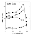
保磁力Hcについての測定結果を他の実施例および比較例の結果と合わせて図5に示す。図5の横軸はアニール温度(℃)であり、縦軸は保磁力Hc(kOe)である。
本実施例1では、アニール処理をしていないサンプルの保磁力Hcは7.1kOeであった。この保磁力は現状の技術レベルにおいて実現されている磁性薄膜の保磁力と比べて同等程度以上であり、本実施例1の磁性薄膜はアニール処理を行わなくても、現状の垂直磁気記録媒体として用いる際の保磁力としては十分な保磁力である。
また、本実施例1では、アニール処理をすることにより、保磁力Hcがさらに大きくなった。図5からわかるように、アニール温度が500℃のときに最も保磁力Hcが大きくなった。その値は10.8kOeであり、10kOeを上回った。前述したように、現状の技術レベルにおいて実現されている磁性薄膜の保磁力Hcは6~7kOe程度であり、本発明者の認識している範囲では、10kOeを超える保磁力Hcを有する磁性薄膜の報告例はなく、本実施例1の磁性薄膜(500℃でアニール処理)が10kOeを超える保磁力Hcを有する磁性薄膜についての初めての例である。
最も大きい保磁力Hcが得られたとき(アニール温度500℃のとき)のM-Hループ(磁化曲線)を、他の実施例および比較例の結果と合わせて図6に示す。図6の横軸は加えた磁場の強さである。図6の縦軸は、入射光の偏光の軸の回転角(カー回転角)を飽和カー回転角で除して規格化した値である。
(実施例2)
実施例2として作製したターゲット全体の組成は、(80Co-20Pt)-30vol%TiO2である。用いる酸化物をTiO2とした以外は実施例1と同様にしてターゲットを作製した。本実施例2で作製したターゲットは、本発明に係るターゲットの範囲に含まれる。また、作製したターゲットを用いて実施例1と同様にして磁気特性測定用サンプルを作製した。
実施例2として作製したターゲット全体の組成は、(80Co-20Pt)-30vol%TiO2である。用いる酸化物をTiO2とした以外は実施例1と同様にしてターゲットを作製した。本実施例2で作製したターゲットは、本発明に係るターゲットの範囲に含まれる。また、作製したターゲットを用いて実施例1と同様にして磁気特性測定用サンプルを作製した。
そして、実施例1と同様にして、目標のアニール温度(200℃、300℃、400℃、450℃、500℃、600℃)でアニール処理を行って室温まで降温した各磁気特性測定用サンプル(計6つ)および室温で成膜した後アニール処理をしていない磁気特性測定用サンプル(1つ)について、それぞれM-Hループ(磁化曲線)を磁気光学カー効果装置を用いて測定した。そして、それぞれのM-Hループ(磁化曲線)から保磁力Hcを読み取った。
保磁力Hcについての測定結果を他の実施例および比較例の結果と合わせて図5に示す。
本実施例2では、アニール処理をしていないサンプルの保磁力Hcは5.8kOeであったが、アニール処理をした場合、アニール温度が500℃のときに最も保磁力Hcが大きくなり、その値は8.6kOeであった。前述したように、現状の技術レベルにおいて実現されている磁性薄膜の保磁力Hcは6~7kOe程度であり、本実施例2の磁性薄膜(500℃でアニール処理)の保磁力Hcは、現状の技術レベルにおいて実現されている磁性薄膜の保磁力Hcを上回っている。
最も大きい保磁力Hcが得られたとき(アニール温度500℃のとき)のM-Hループ(磁化曲線)を、他の実施例および比較例の結果と合わせて図6に示す。
(比較例1)
比較例1として作製したターゲット全体の組成は、(80Co-20Pt)-30vol%SiO2である。用いる酸化物をSiO2とした以外は実施例1と同様にしてターゲットを作製した。本比較例1で作製したターゲットに用いた酸化物はSiO2であり、本発明に係るターゲットの範囲に含まれない。また、作製したターゲットを用いて実施例1と同様にして磁気特性測定用サンプルを作製した。
比較例1として作製したターゲット全体の組成は、(80Co-20Pt)-30vol%SiO2である。用いる酸化物をSiO2とした以外は実施例1と同様にしてターゲットを作製した。本比較例1で作製したターゲットに用いた酸化物はSiO2であり、本発明に係るターゲットの範囲に含まれない。また、作製したターゲットを用いて実施例1と同様にして磁気特性測定用サンプルを作製した。
そして、実施例1と同様にして、目標のアニール温度(200℃、300℃、400℃、450℃、500℃、600℃)でアニール処理を行って室温まで降温した各磁気特性測定用サンプル(計6つ)および室温で成膜した後アニール処理をしていない磁気特性測定用サンプル(1つ)について、それぞれM-Hループ(磁化曲線)を磁気光学カー効果装置を用いて測定した。そして、それぞれのM-Hループ(磁化曲線)から保磁力Hcを読み取った。
保磁力Hcについての測定結果を他の実施例および比較例の結果と合わせて図5に示す。
本比較例1では、アニール処理をしていないサンプルの保磁力Hcは5.2kOeであった。アニール処理をした場合、アニール温度が300℃のときに最も保磁力Hcが大きくなり、その値は5.5kOeであった。
最も大きい保磁力Hcが得られたとき(アニール温度300℃のとき)のM-Hループ(磁化曲線)を、他の実施例および比較例の結果と合わせて図6に示す。
(比較例2)
比較例2として作製したターゲット全体の組成は、(80Co-20Pt)-30vol%Al2O3である。用いる酸化物をAl2O3とした以外は実施例1と同様にしてターゲットを作製した。本比較例2で作製したターゲットに用いた酸化物はAl2O3であり、本発明に係るターゲットの範囲に含まれない。また、作製したターゲットを用いて実施例1と同様にして磁気特性測定用サンプルを作製した。
比較例2として作製したターゲット全体の組成は、(80Co-20Pt)-30vol%Al2O3である。用いる酸化物をAl2O3とした以外は実施例1と同様にしてターゲットを作製した。本比較例2で作製したターゲットに用いた酸化物はAl2O3であり、本発明に係るターゲットの範囲に含まれない。また、作製したターゲットを用いて実施例1と同様にして磁気特性測定用サンプルを作製した。
そして、実施例1と同様にして、目標のアニール温度(200℃、300℃、400℃、450℃、500℃、600℃)でアニール処理を行って室温まで降温した各磁気特性測定用サンプル(計6つ)および室温で成膜した後アニール処理をしていない磁気特性測定用サンプル(1つ)について、それぞれM-Hループ(磁化曲線)を磁気光学カー効果装置を用いて測定した。そして、それぞれのM-Hループ(磁化曲線)から保磁力Hcを読み取った。
保磁力Hcについての測定結果を他の実施例および比較例の結果と合わせて図5に示す。
本比較例2では、アニール処理をしていないサンプルの保磁力Hcは0.9kOeであった。アニール処理をした場合、アニール温度が600℃のときに最も保磁力Hcが大きくなり、その値は2.3kOeであった。
最も大きい保磁力Hcが得られたとき(アニール温度600℃のとき)のM-Hループ(磁化曲線)を、他の実施例および比較例の結果と合わせて図6に示す。
(酸化物についての考察)
実施例1で用いた酸化物はWO3であり、実施例2で用いた酸化物はTiO2であり、比較例1で用いた酸化物はSiO2であり、比較例2で用いた酸化物はAl2O3である。
実施例1で用いた酸化物はWO3であり、実施例2で用いた酸化物はTiO2であり、比較例1で用いた酸化物はSiO2であり、比較例2で用いた酸化物はAl2O3である。
これらの4種類の酸化物が、得られる磁性薄膜の磁気特性にどのような影響を与えているのかについてさらに考察するために、図6に記載したM-Hループ(保磁力Hcが最大となるアニール温度でのアニール処理をした磁気特性測定用サンプルについてのM-Hループ)から、核生成磁場Hn(kOe)およびM-Hループ(磁化曲線)の傾きαをさらに算出した。M-Hループ(磁化曲線)の傾きαは、保磁力Hcを示す点の近傍の領域のデータを用いて、算出式4π×|dM/dH|により算出した。核生成磁場Hn(kOe)およびM-Hループの傾きαの算出結果を、先に記載した保磁力Hcの最大値とともに次の表1にまとめて示す。

表1からわかるように、磁性薄膜の保磁力Hcおよび核生成磁場Hnの値は酸化物としてWO3を用いた実施例1が最大であり、その値はそれぞれ10.8(kOe)、5.5(kOe)である。前述したように、現状の技術レベルにおいて実現されている磁性薄膜の保磁力Hcは6~7kOe程度であり、本発明者の認識している範囲では、10kOeを超える保磁力Hcを有する磁性薄膜の報告例はなく、実施例1の磁性薄膜(500℃でアニール処理)が10kOeを超える保磁力Hcを有する磁性薄膜の初めての例である。
また、酸化物としてWO3を用いた実施例1の磁性薄膜(500℃でのアニール処理後)は、M-Hループの傾きαが1.6と小さく、磁化の反転が急激に生じることは考えにくい。
酸化物としてWO3を用いた実施例1の磁性薄膜(500℃でアニール処理)は、保磁力Hcおよび核生成磁場Hnが大きく、また、M-Hループの傾きαが小さいので、磁気記録膜として用いた場合の記録信号の熱安定性は極めて良好になると考えられる。
また、図5からわかるように、酸化物としてWO3を用いた実施例1の磁性薄膜は、アニール温度が500℃以下の範囲において、アニール温度を上げるほど保磁力Hcが大きくなるので、アニール温度500℃以下のアニール処理によって保磁力Hcが向上するという特性を持った磁性薄膜でもある。
また、図5からわかるように、酸化物としてWO3を用いた実施例1の磁性薄膜は、アニール処理を行わない状態(室温で成膜したままの状態)でも、保磁力Hcが7.1kOeであり、この保磁力は現状の技術レベルにおいて実現されている磁性薄膜の保磁力と比べて同等程度以上である。したがって、本実施例1の磁性薄膜はアニール処理を行わなくても、現状の垂直磁気記録媒体として用いる際の保磁力としては十分な保磁力である。
酸化物としてTiO2を用いた実施例2の磁性薄膜(500℃でアニール処理)の保磁力Hcおよび核生成磁場Hnの値はそれぞれ8.6(kOe)、4.9(kOe)であり、実施例1の磁性薄膜の値を下回るが、現状の磁性薄膜と比べた場合、実現されている保磁力を上回る磁性薄膜であり、磁気記録膜として用いた場合の記録信号の熱安定性は良好になると考えられる。
また、図5からわかるように、酸化物としてTiO2を用いた実施例2の磁性薄膜は、アニール温度が500℃以下の範囲において、アニール温度を上げるほど保磁力Hcが大きくなるので、アニール温度500℃以下のアニール処理によって保磁力Hcが向上するという特性を持った磁性薄膜でもある。
一方、酸化物としてSiO2を用いた比較例1の磁性薄膜および酸化物としてAl2O3を用いた比較例2の磁性薄膜は、アニール処理を行うかどうかに関わらず、保磁力が現状の技術レベルにおいて実現されている磁性薄膜の保磁力(6~7kOe)に到達しておらず、磁気記録膜として用いた場合の記録信号の熱安定性は良好になるとは言い切れないと考えられる。
(実施例1の磁性薄膜のTEM観察)
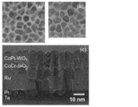
極めて良好な磁気特性の得られた実施例1の磁性薄膜(酸化物としてWO3を用いた磁性薄膜)について、TEMを用いてミクロ構造を確認した。図7に実施例1の磁性薄膜のTEM写真を示す。
極めて良好な磁気特性の得られた実施例1の磁性薄膜(酸化物としてWO3を用いた磁性薄膜)について、TEMを用いてミクロ構造を確認した。図7に実施例1の磁性薄膜のTEM写真を示す。
図7(a)は、アニール処理をしていないCoPt-WO3磁性薄膜の平面TEM写真(磁性薄膜の平面方向の面のTEM写真)であり、図7(b)は、500℃でアニール処理をしたCoPt-WO3磁性薄膜の平面TEM写真である。
図7(a)、(b)の平面TEM写真において、濃い灰色の領域はCoPt合金であり、白色の領域はWO3である。図7(a)、(b)からわかるように、アニール処理の有無にかかわらず、CoPt合金磁性結晶粒はWO3によって1nm程度分離されており、良好なグラニュラ構造となっていることがわかる。
また、平面TEM写真を用いて各CoPt合金磁性結晶粒の領域の面積を100か所以上求め、CoPt合金磁性結晶粒の形状が円柱であると仮定した時の結晶粒径(円柱の直径)を算出したところ、アニール処理をしていない場合は6.4nmであり、500℃のアニール処理をした場合は8nmであった。このことから、アニール処理によってCoPt合金磁性結晶粒が円柱状に成長するものと考えられる。
図7(c)は500℃でアニール処理をしたCoPt-WO3磁性薄膜の断面TEM写真(磁性薄膜の平面と直交する方向の断面のTEM写真)である。この断面TEM写真からわかるように、500℃でアニール処理をしたCoPt-WO3磁性薄膜において、CoPt合金磁性結晶粒が円柱状に成長していることがわかる。
以上説明したように、CoPt-WO3磁性薄膜は、アニール処理の有無にかかわらず、良好なグラニュラ構造となっていることをTEM観察により確認した。また、CoPt-WO3磁性薄膜を500℃でアニール処理をすることにより、CoPt合金磁性結晶粒を円柱状に成長させることができることも確認した。
(好適なアニール温度について)
実施例1、2の磁性薄膜において良好な保磁力Hcが得られたので、実施例1、2の磁性薄膜に対する好適なアニール温度について、図5(アニール温度と保磁力Hcとの関係を示すグラフ)に基づき検討する。
実施例1、2の磁性薄膜において良好な保磁力Hcが得られたので、実施例1、2の磁性薄膜に対する好適なアニール温度について、図5(アニール温度と保磁力Hcとの関係を示すグラフ)に基づき検討する。
図5からわかるように、アニール温度が300℃以上550℃以下の温度範囲にあるとき、実施例1、2の磁性薄膜の保磁力Hcは6.5kOe程度以上になっており、現状の技術水準の磁性薄膜の保磁力Hcと比べて同等以上の値となる。したがって、実施例1、2の磁性薄膜に対するアニール温度は300℃以上550℃以下の温度範囲であることが好ましい。
また、図5からわかるように、アニール温度が400℃以上520℃以下の温度範囲にあるとき、実施例1の磁性薄膜の保磁力Hcは9kOe程度以上になっており、現状の技術水準を上回る保磁力Hcを発現している。また、実施例2の磁性薄膜の保磁力Hcも、アニール温度が400℃以上520℃以下の温度範囲にあるとき、7.1kOe程度以上になっており、現状の技術水準の磁性薄膜と比べて同等以上の保磁力Hcが得られている。したがって、実施例1、2の磁性薄膜に対するアニール温度は400℃以上520℃以下の温度範囲であることがより好ましい。
また、図5からわかるように、アニール温度が460℃以上520℃以下の温度範囲にあるとき、実施例1の磁性薄膜の保磁力Hcは10kOe程度以上になっており、現状の技術水準の磁性薄膜では到達していない保磁力Hcを発現している。また、実施例2の磁性薄膜の保磁力Hcも、アニール温度が460℃以上520℃以下の温度範囲にあるとき、8kOe程度以上になっており、現状の技術水準を上回る保磁力Hcが得られている。したがって、実施例1、2の磁性薄膜に対するアニール温度は460℃以上520℃以下の温度範囲であることがさらに好ましい。
また、図5からわかるように、アニール温度が480℃以上510℃以下の温度範囲にあるとき、実施例1、2の磁性薄膜において保磁力Hcがほぼ最大となる。したがって、実施例1、2の磁性薄膜に対するアニール温度は480℃以上510℃以下の温度範囲であることが特に好ましい。
(アニール処理による保磁力Hc増大の理由についての考察)
実施例1の磁性薄膜では、500℃でアニール処理をすることにより、10.8kOeという大きな保磁力Hcが得られた。アニール処理によって大きな保磁力Hcが得られた理由を考察するために、実施例1の磁性薄膜中のCoPt合金磁性結晶粒の結晶磁気異方性定数Ku grainと異方性磁界Hk grainを算出した。具体的には、CoPt-WO3磁性薄膜の平均磁気特性の値から30vol%のWO3による影響分を計算により除外して、結晶磁気異方性定数Ku grainと異方性磁界Hk grainを算出した。
実施例1の磁性薄膜では、500℃でアニール処理をすることにより、10.8kOeという大きな保磁力Hcが得られた。アニール処理によって大きな保磁力Hcが得られた理由を考察するために、実施例1の磁性薄膜中のCoPt合金磁性結晶粒の結晶磁気異方性定数Ku grainと異方性磁界Hk grainを算出した。具体的には、CoPt-WO3磁性薄膜の平均磁気特性の値から30vol%のWO3による影響分を計算により除外して、結晶磁気異方性定数Ku grainと異方性磁界Hk grainを算出した。
ここで、結晶磁気異方性定数Ku
grainと異方性磁界Hk
grainとの間には、Ku
grain=(Ms
grain×Hk
grain)/2という関係がある。Ms
grainは各結晶粒の飽和磁化であり、試料振動型磁力計で測定した平均飽和磁化の値から算出した。各結晶粒の飽和磁化Ms
grainはアニール処理の有無およびアニール温度に関わらずほぼ一定の値であり、約990emu/cm3であった。
実施例1の磁性薄膜中のCoPt合金磁性結晶粒について算出した結晶磁気異方性定数Ku
grainと異方性磁界Hk
grainをグラフとして表現した図を図8に示す。図8に示すグラフの横軸はアニール温度(℃)であり、縦軸は結晶磁気異方性定数Ku
grain(×106 erg/cm3)および異方性磁界Hk
grain(kOe)である。
図8からわかるように、アニール温度を室温から500℃に増加させると、結晶磁気異方性定数Ku
grainは7.8×10⁶ erg/cm3 から10.4×10⁶ erg/cm3 に増加し、異方性磁界Hk
grainは15.7kOeから21kOeに増加している。この結晶磁気異方性定数Ku
grainと異方性磁界Hk
grainの変化の様子は図5に示す保磁力Hcの変化の様子と同様であることから、アニール処理による保磁力Hcの増大は結晶磁気異方性定数Ku
grainの増大に基づくものであると考えられる。
(CoPt合金の組成についての追加検討)
以上説明した参考例ならびに実施例1、2および比較例1、2の結果から、Co、Pt、および酸化物を含有してなる一方、Crを含有せず、また、前記酸化物としてWO3を有してなるスパッタリングターゲットを用いて、基板を加熱しないで作製した磁性薄膜を、500℃でアニール処理をすることにより、保磁力Hcが10kOeを上回る磁性薄膜を得られることがわかった。
以上説明した参考例ならびに実施例1、2および比較例1、2の結果から、Co、Pt、および酸化物を含有してなる一方、Crを含有せず、また、前記酸化物としてWO3を有してなるスパッタリングターゲットを用いて、基板を加熱しないで作製した磁性薄膜を、500℃でアニール処理をすることにより、保磁力Hcが10kOeを上回る磁性薄膜を得られることがわかった。
しかしながら、実施例1、2および比較例1、2で用いたスパッタリングターゲットにおけるCoとPtの組成は、80Co-20Ptの1種類のみである。
そこで、CoとPtの組成を変えたスパッタリングターゲット(酸化物はWO3を30vol%含有)を用いて、基板を加熱しないで作製した磁性薄膜を500℃でアニール処理をし、該アニール処理をした磁性薄膜の保磁力Hcと核生成磁場Hnを測定して、本発明の効果が発現するスパッタリングターゲット中のCoとPtの組成範囲について検討した。
追加検討したスパッタリングターゲット(実施例3~7、比較例3、4)中のCoとPtの組成は、実施例3が90Co-10Ptであり、実施例4が85Co-15Ptであり、実施例5が50Co-50Ptであり、実施例6が25Co-75Ptであり、実施例7が20Co-80Ptである。また、比較例3のスパッタリングターゲット中の金属成分はCoのみであり、比較例4のスパッタリングターゲット中の金属成分はPtのみである。CoとPtの組成を変えた以外は実施例1と同様にしてターゲットを作製し、実施例1と同様にして磁性薄膜の保磁力Hcと核生成磁場Hnを測定した。その測定結果を実施例1の測定結果とともに次の表2に示す。

表2からわかるように、本発明の範囲内のスパッタリングターゲット(実施例1、実施例3~7)を用いて作製した磁性薄膜の500℃アニール処理後の保磁力Hcはいずれも6.8kOe以上であり、現状の技術水準の保持力と比べて同等の保磁力以上であった。特に、実施例1、5、6は、10kOe以上の保磁力であり、極めて大きな保磁力が得られた。
一方、スパッタリングターゲット中の金属成分がCoのみであり本発明の範囲外である比較例3のスパッタリングターゲット、およびスパッタリングターゲット中の金属成分がPtのみであり本発明の範囲外である比較例4のスパッタリングターゲットを用いて作製した磁性薄膜の500℃アニール処理後の保磁力Hcは、それぞれ0.5kOe、0.0kOeと小さかった。
(酸化物含有量についての追加検討)
前述したように、本発明の範囲内のスパッタリングターゲット(実施例1、実施例3~7)を用いて作製した磁性薄膜の500℃アニール処理後の保磁力Hcはいずれも6.8kOe以上であり、現状の技術水準の保持力と比べて同等の保磁力以上であり、良好な結果が得られた。
前述したように、本発明の範囲内のスパッタリングターゲット(実施例1、実施例3~7)を用いて作製した磁性薄膜の500℃アニール処理後の保磁力Hcはいずれも6.8kOe以上であり、現状の技術水準の保持力と比べて同等の保磁力以上であり、良好な結果が得られた。
しかしながら、実施例1、実施例3~7で用いたスパッタリングターゲットにおけるWO3の含有量は、30vol%の1種類のみである。
そこで、WO3の含有量を変えたスパッタリングターゲット(CoとPtの組成は80Co-20Pt)を用いて、基板を加熱しないで作製した磁性薄膜を500℃でアニール処理をし、該アニール処理をした磁性薄膜の保磁力Hcと核生成磁場Hnを測定して、本発明の効果が発現するスパッタリングターゲット中のWO3の含有量の範囲について検討した。
追加検討したスパッタリングターゲット(実施例8~13、比較例5)中のWO3の含有量は、実施例8が10vol%であり、実施例9が20vol%であり、実施例10が25vol%であり、実施例11が35vol%であり、実施例12が40vol%であり、実施例13が50vol%であり、比較例5が0vol%である。WO3の含有量を変えた以外は実施例1と同様にしてターゲットを作製し、実施例1と同様にして磁性薄膜の保磁力Hcと核生成磁場Hnを測定した。その測定結果を実施例1の測定結果とともに次の表3に示す。
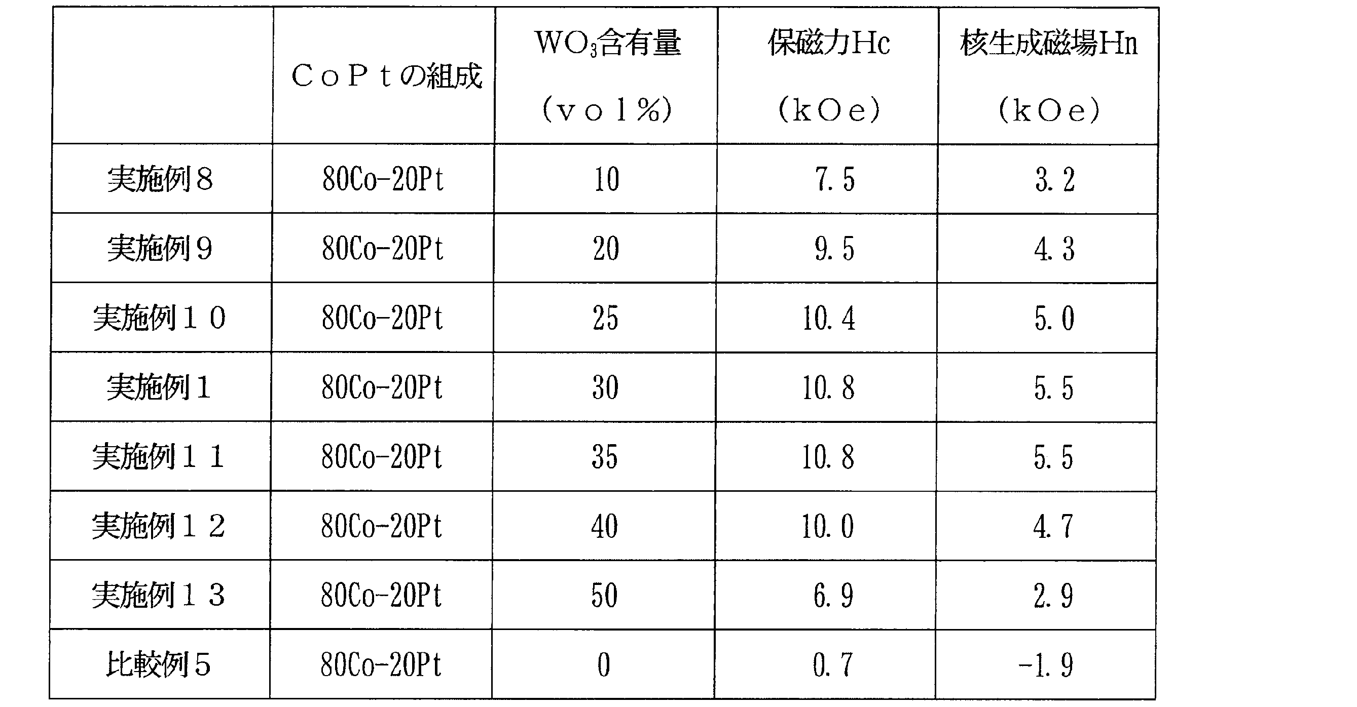
表3からわかるように、本発明の範囲内のスパッタリングターゲット(実施例1、実施例8~13)を用いて作製した磁性薄膜の500℃アニール処理後の保磁力Hcはいずれも6.9kOe以上であり、現状の技術水準の保持力と比べて同等の保磁力以上であった。特に、実施例1、10、11、12は、10kOe以上の保磁力であり、極めて大きな保磁力が得られた。
一方、WO3含有量が0であり、本発明の範囲外である比較例5のスパッタリングターゲットを用いて作製した磁性薄膜の500℃アニール処理後の保磁力Hcは0.7kOeと小さかった。
Claims (20)
- 金属Co、金属Pt、および酸化物を含有してなるスパッタリングターゲットであって、
金属Crを含有せず、
かつ、前記酸化物は、WO3およびTiO2のうちの少なくともいずれか一方を有してなることを特徴とするスパッタリングターゲット。 - 金属Coと金属Ptの合計に対して金属Coを20~90at%含有することを特徴とする請求項1に記載のスパッタリングターゲット。
- 前記酸化物は、WO3およびTiO2のうちの少なくともいずれか一方であることを特徴とする請求項1または2に記載のスパッタリングターゲット。
- 前記酸化物は、WO3を有してなることを特徴とする請求項1または2に記載のスパッタリングターゲット。
- 前記酸化物は、WO3であることを特徴とする請求項1または2に記載のスパッタリングターゲット。
- 前記酸化物を、10~50vol%含有することを特徴とする請求項1~5のいずれかに記載のスパッタリングターゲット。
- 前記酸化物を、25~35vol%含有することを特徴とする請求項1~5のいずれかに記載のスパッタリングターゲット。
- 前記スパッタリングターゲットは、磁性薄膜の作製に使用可能なことを特徴とする請求項1~7のいずれかに記載のスパッタリングターゲット。
- 前記スパッタリングターゲットを用いて作製された磁性薄膜に対して300℃以上550℃以下の温度範囲でアニール処理を行うことにより、該磁性薄膜の保磁力を6kOe以上とすることができることを特徴とする請求項8に記載のスパッタリングターゲット。
- 前記酸化物はWO3を有してなり、
前記スパッタリングターゲットを用いて作製された磁性薄膜に対して400℃以上520℃以下の温度範囲でアニール処理を行うことにより、該磁性薄膜の保磁力を9kOe以上とすることができることを特徴とする請求項8に記載のスパッタリングターゲット。 - 前記酸化物はWO3を有してなり、
前記スパッタリングターゲットを用いて作製された磁性薄膜に対して460℃以上520℃以下の温度範囲でアニール処理を行うことにより、該磁性薄膜の保磁力を10kOe以上とすることができることを特徴とする請求項8に記載のスパッタリングターゲット。 - 前記アニール処理を行った後の前記磁性薄膜の構造がグラニュラ構造であることを特徴とする請求項9~11のいずれかに記載のスパッタリングターゲット。
- CoおよびPtを含有する一方Crを含有しないCoPt合金粉末をアトマイズ法で作製する工程と、
前記作製したCoPt合金粉末と、酸化物粉末とを混合分散して加圧焼結用混合粉末を作製する工程と、
前記作製した加圧焼結用混合粉末を加圧焼結する工程と、
を有し、
前記酸化物粉末は、WO3およびTiO2のうちの少なくともいずれか一方を有してなることを特徴とするスパッタリングターゲットの製造方法。 - Co粉末と、Pt粉末と、酸化物粉末とを混合分散して加圧焼結用混合粉末を得る工程と、
前記得られた加圧焼結用混合粉末を加圧焼結する工程と、
を有し、
前記酸化物粉末は、WO3およびTiO2のうちの少なくともいずれか一方を有してなることを特徴とするスパッタリングターゲットの製造方法。 - 得られるスパッタリングターゲットは、金属Coと金属Ptの合計に対して金属Coを20~90at%含有することを特徴とする請求項13または14に記載のスパッタリングターゲットの製造方法。
- 前記酸化物粉末は、WO3およびTiO2のうちの少なくともいずれか一方であることを特徴とする請求項13~15のいずれかに記載のスパッタリングターゲットの製造方法。
- 前記酸化物粉末は、WO3を有してなることを特徴とする請求項13~15のいずれかに記載のスパッタリングターゲットの製造方法。
- 前記酸化物粉末は、WO3であることを特徴とする請求項13~15のいずれかに記載のスパッタリングターゲットの製造方法。
- 前記酸化物粉末の前記加圧焼結用混合粉末の全体に対する体積分率が10~50vol%であることを特徴とする請求項13~18のいずれかに記載のスパッタリングターゲットの製造方法。
- 前記酸化物粉末の前記加圧焼結用混合粉末の全体に対する体積分率が25~35vol%であることを特徴とする請求項13~18のいずれかに記載のスパッタリングターゲットの製造方法。
Priority Applications (3)
| Application Number | Priority Date | Filing Date | Title |
|---|---|---|---|
| CN201580021850.2A CN106232862B (zh) | 2014-05-02 | 2015-04-14 | 溅射靶及其制造方法 |
| US15/304,938 US10636633B2 (en) | 2014-05-02 | 2015-04-14 | Sputtering target and process for production thereof |
| SG11201608581XA SG11201608581XA (en) | 2014-05-02 | 2015-04-14 | Sputtering target and process for production thereof |
Applications Claiming Priority (2)
| Application Number | Priority Date | Filing Date | Title |
|---|---|---|---|
| JP2014-095566 | 2014-05-02 | ||
| JP2014095566A JP6416497B2 (ja) | 2014-05-02 | 2014-05-02 | スパッタリングターゲットおよびその製造方法 |
Publications (1)
| Publication Number | Publication Date |
|---|---|
| WO2015166795A1 true WO2015166795A1 (ja) | 2015-11-05 |
Family
ID=54358530
Family Applications (1)
| Application Number | Title | Priority Date | Filing Date |
|---|---|---|---|
| PCT/JP2015/061409 Ceased WO2015166795A1 (ja) | 2014-05-02 | 2015-04-14 | スパッタリングターゲットおよびその製造方法 |
Country Status (7)
| Country | Link |
|---|---|
| US (1) | US10636633B2 (ja) |
| JP (1) | JP6416497B2 (ja) |
| CN (1) | CN106232862B (ja) |
| MY (1) | MY177222A (ja) |
| SG (1) | SG11201608581XA (ja) |
| TW (1) | TWI585213B (ja) |
| WO (1) | WO2015166795A1 (ja) |
Cited By (4)
| Publication number | Priority date | Publication date | Assignee | Title |
|---|---|---|---|---|
| TWI642798B (zh) * | 2015-11-27 | 2018-12-01 | 日商田中貴金屬工業股份有限公司 | 濺鍍靶 |
| WO2021221096A1 (ja) * | 2020-05-01 | 2021-11-04 | 田中貴金属工業株式会社 | 面内磁化膜、面内磁化膜多層構造、ハードバイアス層、磁気抵抗効果素子、およびスパッタリングターゲット |
| US11810700B2 (en) | 2018-10-30 | 2023-11-07 | Tanaka Kikinzoku Kogyo K.K. | In-plane magnetized film, in-plane magnetized film multilayer structure, hard bias layer, magnetoresistive element, and sputtering target |
| WO2025094868A1 (ja) * | 2023-10-30 | 2025-05-08 | 田中貴金属工業株式会社 | 磁気記録媒体用スパッタリングターゲット |
Families Citing this family (7)
| Publication number | Priority date | Publication date | Assignee | Title |
|---|---|---|---|---|
| MY192454A (en) * | 2016-11-01 | 2022-08-21 | Tanaka Precious Metal Ind | Sputtering target for magnetic recording media |
| TWI671418B (zh) * | 2017-09-21 | 2019-09-11 | 日商Jx金屬股份有限公司 | 濺鍍靶、積層膜之製造方法、積層膜及磁記錄媒體 |
| TWI679291B (zh) * | 2017-09-21 | 2019-12-11 | 日商Jx金屬股份有限公司 | 濺鍍靶、積層膜之製造方法、積層膜及磁記錄媒體 |
| DE102018112335A1 (de) * | 2018-05-23 | 2019-11-28 | Hartmetall-Werkzeugfabrik Paul Horn Gmbh | Magnetronsputtervorrichtung |
| JP7438845B2 (ja) * | 2020-05-01 | 2024-02-27 | 田中貴金属工業株式会社 | 面内磁化膜、面内磁化膜多層構造、ハードバイアス層、および磁気抵抗効果素子 |
| JP7431660B2 (ja) * | 2020-05-01 | 2024-02-15 | 田中貴金属工業株式会社 | 面内磁化膜多層構造、ハードバイアス層、および磁気抵抗効果素子 |
| JP7438074B2 (ja) * | 2020-09-25 | 2024-02-26 | シチズンファインデバイス株式会社 | 金属-酸化物系グラニュラー膜の製造方法 |
Citations (2)
| Publication number | Priority date | Publication date | Assignee | Title |
|---|---|---|---|---|
| JP2000282229A (ja) * | 1999-03-29 | 2000-10-10 | Hitachi Metals Ltd | CoPt系スパッタリングターゲットおよびその製造方法ならびにこれを用いた磁気記録膜およびCoPt系磁気記録媒体 |
| WO2010074171A1 (ja) * | 2008-12-26 | 2010-07-01 | 三井金属鉱業株式会社 | スパッタリングターゲットおよび膜の形成方法 |
Family Cites Families (6)
| Publication number | Priority date | Publication date | Assignee | Title |
|---|---|---|---|---|
| US5989728A (en) * | 1994-11-02 | 1999-11-23 | International Business Machines Corporation | Thin film magnetic recording medium having high coercivity |
| JP4213001B2 (ja) * | 2003-09-25 | 2009-01-21 | 株式会社東芝 | 垂直磁気記録媒体、及び磁気記録再生装置 |
| US20060246323A1 (en) * | 2005-04-27 | 2006-11-02 | Seagate Technology Llc | Epitaxially grown non-oxide magnetic layers for granular perpendicular magnetic recording media applications |
| US7879470B2 (en) * | 2007-11-15 | 2011-02-01 | Hitachi Global Storage Technologies Netherlands B.V. | Apparatus, system, and method for the selection of perpendicular media segregant materials |
| JP5583997B2 (ja) * | 2009-03-30 | 2014-09-03 | ダブリュディ・メディア・シンガポール・プライベートリミテッド | 垂直磁気記録媒体 |
| US8941950B2 (en) * | 2012-05-23 | 2015-01-27 | WD Media, LLC | Underlayers for heat assisted magnetic recording (HAMR) media |
-
2014
- 2014-05-02 JP JP2014095566A patent/JP6416497B2/ja active Active
-
2015
- 2015-04-14 SG SG11201608581XA patent/SG11201608581XA/en unknown
- 2015-04-14 WO PCT/JP2015/061409 patent/WO2015166795A1/ja not_active Ceased
- 2015-04-14 MY MYPI2016703748A patent/MY177222A/en unknown
- 2015-04-14 CN CN201580021850.2A patent/CN106232862B/zh not_active Expired - Fee Related
- 2015-04-14 US US15/304,938 patent/US10636633B2/en not_active Expired - Fee Related
- 2015-04-28 TW TW104113527A patent/TWI585213B/zh active
Patent Citations (2)
| Publication number | Priority date | Publication date | Assignee | Title |
|---|---|---|---|---|
| JP2000282229A (ja) * | 1999-03-29 | 2000-10-10 | Hitachi Metals Ltd | CoPt系スパッタリングターゲットおよびその製造方法ならびにこれを用いた磁気記録膜およびCoPt系磁気記録媒体 |
| WO2010074171A1 (ja) * | 2008-12-26 | 2010-07-01 | 三井金属鉱業株式会社 | スパッタリングターゲットおよび膜の形成方法 |
Non-Patent Citations (3)
| Title |
|---|
| JUN ARIAKE: "Improvement of magnetic and R/W performance by annealing on Co-Pt-TiO_ 2 granular films for perpendicular magnetic recording media", IEICE TECHNICAL REPORT, 14 November 2008 (2008-11-14), pages 31 - 36 * |
| KAZUYOSHI HASHIMOTO: "Nano-structure and Magnetic Property of CoPt-TiO_2 Perpendicular Magnetic Recording Film", IEICE TECHNICAL REPORT, vol. 108, no. 124, 3 July 2008 (2008-07-03), pages 27 - 31 * |
| NOLAN, T.P.: "Microstructure and Exchange Coupling of Segregated Oxide Perpendicular Recording Media", TRANSACTIONS ON MAGNETICS, vol. 43, no. 2, February 2007 (2007-02-01), pages 639 - 644, XP011183782, ISSN: 0018-9464 * |
Cited By (6)
| Publication number | Priority date | Publication date | Assignee | Title |
|---|---|---|---|---|
| TWI642798B (zh) * | 2015-11-27 | 2018-12-01 | 日商田中貴金屬工業股份有限公司 | 濺鍍靶 |
| US11072851B2 (en) | 2015-11-27 | 2021-07-27 | Tanaka Kikinzoku Kogyo K.K. | Sputtering target |
| US11810700B2 (en) | 2018-10-30 | 2023-11-07 | Tanaka Kikinzoku Kogyo K.K. | In-plane magnetized film, in-plane magnetized film multilayer structure, hard bias layer, magnetoresistive element, and sputtering target |
| WO2021221096A1 (ja) * | 2020-05-01 | 2021-11-04 | 田中貴金属工業株式会社 | 面内磁化膜、面内磁化膜多層構造、ハードバイアス層、磁気抵抗効果素子、およびスパッタリングターゲット |
| JP7529433B2 (ja) | 2020-05-01 | 2024-08-06 | 田中貴金属工業株式会社 | 面内磁化膜、面内磁化膜多層構造、ハードバイアス層、磁気抵抗効果素子、およびスパッタリングターゲット |
| WO2025094868A1 (ja) * | 2023-10-30 | 2025-05-08 | 田中貴金属工業株式会社 | 磁気記録媒体用スパッタリングターゲット |
Also Published As
| Publication number | Publication date |
|---|---|
| TWI585213B (zh) | 2017-06-01 |
| JP6416497B2 (ja) | 2018-10-31 |
| US10636633B2 (en) | 2020-04-28 |
| US20170194131A1 (en) | 2017-07-06 |
| CN106232862B (zh) | 2019-11-26 |
| MY177222A (en) | 2020-09-09 |
| JP2015212409A (ja) | 2015-11-26 |
| TW201606092A (zh) | 2016-02-16 |
| CN106232862A (zh) | 2016-12-14 |
| SG11201608581XA (en) | 2016-11-29 |
Similar Documents
| Publication | Publication Date | Title |
|---|---|---|
| JP6416497B2 (ja) | スパッタリングターゲットおよびその製造方法 | |
| CN109923610B (zh) | 磁记录介质用溅射靶 | |
| CN112106134B (zh) | 磁记录介质用溅射靶 | |
| TWI753073B (zh) | 磁性材濺鍍靶及其製造方法 | |
| US20210269911A1 (en) | Sputtering target | |
| TWI778215B (zh) | 濺鍍靶 | |
| TWI812869B (zh) | 磁性記錄媒體用濺鍍靶 | |
| TW201915204A (zh) | 濺鍍靶、積層膜之製造方法、積層膜及磁記錄媒體 | |
| JP7610224B2 (ja) | 熱アシスト磁気記録媒体用スパッタリングターゲット | |
| TWI671418B (zh) | 濺鍍靶、積層膜之製造方法、積層膜及磁記錄媒體 | |
| TW202330964A (zh) | 用以製造熱輔助磁記錄媒體之濺鍍靶 | |
| JP2011081859A (ja) | 磁気記録媒体膜形成用スパッタリングターゲット及びその製造方法 |
Legal Events
| Date | Code | Title | Description |
|---|---|---|---|
| 121 | Ep: the epo has been informed by wipo that ep was designated in this application |
Ref document number: 15786761 Country of ref document: EP Kind code of ref document: A1 |
|
| DPE1 | Request for preliminary examination filed after expiration of 19th month from priority date (pct application filed from 20040101) | ||
| WWE | Wipo information: entry into national phase |
Ref document number: 15304938 Country of ref document: US |
|
| NENP | Non-entry into the national phase |
Ref country code: DE |
|
| 122 | Ep: pct application non-entry in european phase |
Ref document number: 15786761 Country of ref document: EP Kind code of ref document: A1 |