WO2015166570A1 - 半導体集積回路のレイアウト設計方法および装置 - Google Patents
半導体集積回路のレイアウト設計方法および装置 Download PDFInfo
- Publication number
- WO2015166570A1 WO2015166570A1 PCT/JP2014/062054 JP2014062054W WO2015166570A1 WO 2015166570 A1 WO2015166570 A1 WO 2015166570A1 JP 2014062054 W JP2014062054 W JP 2014062054W WO 2015166570 A1 WO2015166570 A1 WO 2015166570A1
- Authority
- WO
- WIPO (PCT)
- Prior art keywords
- mask
- integrated circuit
- semiconductor integrated
- defect
- layout design
- Prior art date
- Legal status (The legal status is an assumption and is not a legal conclusion. Google has not performed a legal analysis and makes no representation as to the accuracy of the status listed.)
- Ceased
Links
Images







Classifications
-
- G—PHYSICS
- G03—PHOTOGRAPHY; CINEMATOGRAPHY; ANALOGOUS TECHNIQUES USING WAVES OTHER THAN OPTICAL WAVES; ELECTROGRAPHY; HOLOGRAPHY
- G03F—PHOTOMECHANICAL PRODUCTION OF TEXTURED OR PATTERNED SURFACES, e.g. FOR PRINTING, FOR PROCESSING OF SEMICONDUCTOR DEVICES; MATERIALS THEREFOR; ORIGINALS THEREFOR; APPARATUS SPECIALLY ADAPTED THEREFOR
- G03F1/00—Originals for photomechanical production of textured or patterned surfaces, e.g., masks, photo-masks, reticles; Mask blanks or pellicles therefor; Containers specially adapted therefor; Preparation thereof
- G03F1/22—Masks or mask blanks for imaging by radiation of 100nm or shorter wavelength, e.g. X-ray masks, extreme ultraviolet [EUV] masks; Preparation thereof
- G03F1/24—Reflection masks; Preparation thereof
-
- G—PHYSICS
- G03—PHOTOGRAPHY; CINEMATOGRAPHY; ANALOGOUS TECHNIQUES USING WAVES OTHER THAN OPTICAL WAVES; ELECTROGRAPHY; HOLOGRAPHY
- G03F—PHOTOMECHANICAL PRODUCTION OF TEXTURED OR PATTERNED SURFACES, e.g. FOR PRINTING, FOR PROCESSING OF SEMICONDUCTOR DEVICES; MATERIALS THEREFOR; ORIGINALS THEREFOR; APPARATUS SPECIALLY ADAPTED THEREFOR
- G03F1/00—Originals for photomechanical production of textured or patterned surfaces, e.g., masks, photo-masks, reticles; Mask blanks or pellicles therefor; Containers specially adapted therefor; Preparation thereof
- G03F1/68—Preparation processes not covered by groups G03F1/20 - G03F1/50
- G03F1/70—Adapting basic layout or design of masks to lithographic process requirements, e.g., second iteration correction of mask patterns for imaging
-
- G—PHYSICS
- G06—COMPUTING OR CALCULATING; COUNTING
- G06F—ELECTRIC DIGITAL DATA PROCESSING
- G06F30/00—Computer-aided design [CAD]
Definitions
- the present invention relates to a layout design method and apparatus for a semiconductor integrated circuit, and is suitably used, for example, in producing a pattern layout for an EUV (Extreme Ultra-Violet) mask.
- EUV Extra-Violet
- EUV mask blanks utilize reflections from 40-60 multilayers. Therefore, a mask blank for EUV exposure has a much higher probability of occurrence of defects than a mask blank for optical exposure. Furthermore, it is extremely difficult to correct defects that have occurred. Specifically, in order to correct the mask blank, the multilayer film is once peeled off, foreign substances are removed, and then the multilayer film is formed again. In this case, there should be no significant difference in the reflectance and phase of the multilayer film with or without correction, and there should be no mismatch at the boundary between the corrected portion and the uncorrected portion. Thus, in consideration of the labor and cost for correction, it is practically impossible to correct the defect of the mask blank for EUV exposure.
- Patent Documents 1 to 4 have proposed a method of manufacturing a mask using a defective mask blank.
- the methods of these documents are common in that defect information including a defect type and defect coordinates is given to a mask blank.
- the EUV mask has a Mo / Si (molybdenum / silicon) multilayer film as a reflective layer, a SiO 2 (silicon dioxide) film, and a Ta (tantalum) film as a light-absorbing absorbing layer laminated on the substrate.
- the Ta film is processed into a pattern. By superimposing the defect portion on the pattern of the Ta film as an absorption layer, the influence of the defect is removed.
- Patent Document 1 rotates the mask blank in a plane parallel to the main surface of the mask blank.
- Patent Document 2 JP 2001-033941
- Patent Document 4 JP 2004-170948
- a circuit pattern is used as a mask blank. Move in the in-plane direction, rotate in the plane, or change the magnification of the circuit pattern.
- the position of the circuit pattern formed on the mask blank is almost determined due to the limitations of the exposure apparatus, and the degree of freedom of arrangement of the circuit pattern on the mask blank is not large. For this reason, when the number of defects is relatively large like a mask for EUV exposure, it is difficult to form a circuit pattern so as to avoid all the defective portions by the method described in the above document. As a result, when the photomask is remanufactured, problems such as an increase in cost, a delay in delivery time, and waste of resources arise.
- the prohibited area is set based on the defect information of the mask blank.
- the placement and routing tool places a plurality of functional modules while avoiding the set prohibited area, and generates a wiring pattern between the plurality of functional modules while avoiding the prohibited area.
- a semiconductor integrated circuit device can be manufactured using a mask including a defect.
- FIG. 3 is a flowchart showing a mask manufacturing procedure for a semiconductor integrated circuit including the layout design method according to the first embodiment. It is a flowchart which shows the preparation procedure of the defect information accompanying a mask blank. It is a top view which shows typically the example of the defect on a mask blank, and the dummy pattern which covers it.
- 1 is a configuration diagram of a computer system for realizing a layout design method for a semiconductor integrated circuit according to a first embodiment
- 2 is a flowchart showing details of a layout design procedure of FIG. 1. It is a top view which shows typically the logical sum of the dummy pattern formed on the several mask blanks. It is a top view which shows an example of a floor plan typically.
- FIG. 10 is a cross-sectional view taken along line XX in FIG. 9.
- FIG. 10 is a plan view schematically showing a mask layout for forming the gate electrode of FIG. 9.
- 10 is a flowchart showing a layout design procedure in the layout design method for a semiconductor integrated circuit according to the second embodiment.
- it is sectional drawing which shows an example of a floor plan typically.
- 10 is a flowchart showing a layout design procedure in the layout design method for a semiconductor integrated circuit according to the third embodiment.
- FIG. 1 is a flowchart showing a mask manufacturing procedure for a semiconductor integrated circuit including the layout design method according to the first embodiment.
- the flowchart of FIG. 1 is used, for example, when manufacturing a semiconductor integrated circuit device such as a semiconductor element, a liquid crystal display element, and an imaging element (CCD: Charge-Coupled Device), or when manufacturing a micro device such as a thin film magnetic head.
- CCD Charge-Coupled Device
- the present invention relates to a necessary mask manufacturing procedure.
- the logic design is performed using a computer system such as CAD (Computer Aided Design). (Logic synthesis) The design proceeds in the order of S105, logic verification S110, layout design S115, and layout verification S120.
- the netlist DT10 is created by logically synthesizing digital circuits described in HDL (Hardware Description Language).
- HDL Hardware Description Language
- the operation of assigning gates and nets (connections) to logic blocks and I / O (Input / Output) pins of FPGAs (Field-Programmable Gate Arrays) according to the netlist information is called placement and wiring.
- This placement and routing work is automatically performed by the FPGA development tool. By giving timing constraints and circuit area constraints to the FPGA development tool, it is possible to realize placement and routing that meets the constraints to some extent.
- the above HDL is a programming language that describes hardware operations and connections.
- VHDL is based on the US Department of Defense delivery specification, VHSIC (Very High Speed Integrated Circuits), Hardware Description Language, abbreviated as VHDL, and later standardized as IEEE1076.
- Verilog HDL was born as a language for commercial simulation tools of private companies and has been standardized as IEEE 1364.
- Verilog HDL and VHDL are languages that can handle everything from high-level descriptions to structural descriptions such as component connections.
- the cell library DT12 is a database in which a large number of layout-designed macro cells (functional modules) are collected.
- the cell library DT12 stores data necessary for designing an LSI (Large Scale Integration) such as logic functions, electrical characteristics, and pattern layout.
- Functional modules include analog circuits such as ADC (Analog-to-Digital Converter), DAC (Digital-to-Analog Converter), and PLL (Phase Locked Loop), memory circuits such as SRAM and flash memory, inverters, capacitors A wide variety of elements, resistors, coils, I / O circuits, etc.
- the cell library DT12 is used in the logic design S105 and the layout design S115.
- an automatic placement and routing tool is used to determine the placement of cells and macrocells on the chip (floor plan), and a plurality of cells and a plurality of macrocells. Wiring between each other. As a result, a layout pattern DT16 on the photomask is obtained.
- the placement and routing tool arranges various functional modules and wires the arranged functional modules to design a semiconductor integrated circuit product. At this time, it is particularly important to reduce the chip area and match the signal timing.
- a redundant inverter may be inserted to adjust the timing. However, as the number of such redundant circuits increases, the chip area increases, so that optimization of reduction of the chip area and signal timing matching is performed.
- the place-and-route tool refers to a computer program that realizes the design of a semiconductor integrated circuit, or a computer system in which the program is installed in the computer and the semiconductor integrated circuit can be designed.
- the FPGA In designing the FPGA, it is necessary to input some constraint conditions into the development tool before performing the logic synthesis S105 and the layout design S115 so that the operation as expected by the designer is realized. In order to reduce design rework, shorten the chip development period, and avoid unnecessary chip costs and development costs, it is important to set the constraints correctly. To set the constraints, use the wizard that comes with the development tool, or you can directly import the text file. If the constraints are set correctly, finally, the development tool automatically optimizes the circuit configuration of the chip so as to satisfy the set constraints.
- the pattern layout design method of the semiconductor integrated circuit device is characterized in that the defect information of the mask blank is used as a constraint condition.
- the defect information refers to information such as the position and size of a defect present on the mask blank that cannot be removed by cleaning or correction.
- a flag figure (dummy pattern) is generated so as to cover the defect.
- the size of the flag figure is set to a minimum size necessary to cover the defect after satisfying the condition that the exposure resolution is at least the minimum resolution.
- the shape of the flag figure is not particularly limited, such as a rectangle or a circle.
- the generated flag graphic is stored in the defect information library DT14 in a standard format such as GDS or OASIS as information accompanying the mask blank. If the GUI (Graphical User Interface) is not used, the CSV format may be used as a format for saving the flag graphic.
- the flag graphic information is output as a placement constraint condition from the defect information library DT14 to the layout design placement and routing tool during layout design.
- the placement and routing tool can place functional modules by avoiding flag figures, or connect modules by avoiding flag figures. Since the flag figure is a defect, the integrated circuit product can be designed while avoiding the defect of the mask blank.
- a mask is manufactured by performing mask drawing using the design data (step S125).
- a drawing apparatus using an electron beam (EB) or a laser beam
- EB electron beam
- a mask having a plurality of patterns is formed.
- a photomask in addition to a transmissive mask for light exposure, a multilayer film reflective mask for EUV exposure has recently been put into practical use.
- the completed mask is used for manufacturing semiconductor integrated circuit products.
- the integrated circuit pattern is collectively exposed on the semiconductor substrate by a projection optical system using ultraviolet (UV) light or EUV light. That is, the photomask pattern image is projected onto a wafer, a glass plate, or the like coated with a photoresist. Further, by repeating such operations, an element isolation structure, a well, a diffusion region, a gate electrode layer, a multilayer wiring layer, and the like are sequentially formed, and a semiconductor integrated circuit device is completed.
- UV ultraviolet
- EUV light EUV light
- FIG. 2 is a flowchart showing a procedure for creating defect information associated with a mask blank.
- a mask blank is created (step S200).
- a light shielding film is formed on one main surface of the transparent substrate.
- an antireflection film may be formed on the surface.
- a 40-60 layer multilayer reflective film made of Si and Mo is formed on one main surface of a substrate, an SiO 2 film is further formed thereon, and a Ta layer as an absorbing layer is further formed thereon. A film is formed.
- the mask blank is cleaned in order to remove foreign matter adhering to the mask surface (step S205). Subsequently, the defect on the mask blank is inspected (step S210).
- a defect inspection method there are known methods such as a method using scattered light, die-by-die, and die-to-database.
- step S210 If there is a defect that can be corrected (NO in step S215, YES in step S220), the defect is inspected again after attempting to correct the defect (step S225) (step S210).
- step S220 the position and size of the defect are measured.
- the position of the defect is measured with reference to the position of a fiducial mark on the mask blank.
- a dummy pattern (flag figure) is generated in the recognition layer in the minimum area covering the defect (step S235).
- the generated dummy pattern is stored in the defect information library DT14 in association with the mask blank (step S240).
- FIG. 3 is a plan view schematically showing an example of a defect on a mask blank and a dummy pattern covering the defect.
- FIG. 3 for the sake of simplicity, a case where one defect occurs in each mask is shown. However, in reality, a plurality of defects may occur in one mask. In some cases, defects can be realized. Further, in FIG. 3, defects are actually shown as large as possible for ease of illustration, but the actual defect size is about several ⁇ m at most.
- EUV exposure is performed on the masks M1 to M4 of the STI (Shallow Trench Isolation) layer, the gate electrode layer, the contact layer, and the first metal wiring layer (M1) that particularly require pattern accuracy.
- defects DF1 to DF5 are found for these main masks M1 to M4 and spare mask M5 as shown in FIG.
- dummy patterns DP1 to DP5 are respectively generated in the recognition layer in the minimum area covering the defect.
- the generated dummy pattern is stored in the defect information library DT14 of FIG. 1 in association with the corresponding mask blank.
- Mask blanks are stocked with defect information.
- the mask since the mask may be revised in the future in the new product, it is preferable to store defect information for the spare mask blanks in the library and stock the necessary number of mask blanks.
- the mask pattern (the light shielding film in the case of an optical mask, and the multilayer reflection film and the absorption film in the case of an EUV mask) is peeled off, and a light shielding film or a multilayer reflection film is formed again. It is preferable to form a mask blank.
- the defect that cannot be corrected may disappear, or even if the defect is reproduced at the same position, it can be used for the next mask revision of the same mask set. If an uncorrectable defect occurs in another position, it cannot be used for the same mask set, but it can be used for the next mask set by measuring the position and size of the defect. Can be used.
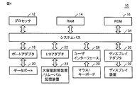
- FIG. 4 is a configuration diagram of a computer system for realizing the layout design method of the semiconductor integrated circuit according to the first embodiment.
- the computer system 10 includes one or more processors (CPU: Central Processing Unit) 12, a RAM (Random Access Memory) 14, and a ROM (Read Only Memory) 16.
- the ROM 16 stores a basic operation system of the computer, and the RAM 14 stores applications and programs necessary for the current processing in the processor 12.
- Data to be processed by the processor is input from the port adapter 18 and the I / O adapter 22 via the system bus 34.
- a design program and data to be processed are input from a large-capacity storage device (such as a hard disk) or a removable storage device (such as a magnetic disk, an optical disk, or a flexible disk) 24 via an I / O adapter 22 or a port.
- the data to be processed includes the net list DT10, the cell library DT12, the defect information library DT14, the layout pattern DT16, and the like shown in FIG.
- the user performs an operation with a mouse and a keyboard via the user interface adapter 26.
- the processing result by the processor 12 is displayed on a display device 32 such as a CRT (Cathode Ray Tube) or a liquid crystal display via the display adapter 30.
- a display device 32 such as a CRT (Cathode Ray Tube) or a liquid crystal display via the display adapter 30.
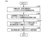
- FIG. 5 is a flowchart showing details of the layout design procedure of FIG. Each procedure shown in FIG. 5 is realized by executing a program such as a placement and routing tool in the processor 12 of FIG.
- the processor 12 acquires defect information corresponding to a plurality of necessary mask blanks including a spare from the defect information library DT14 of FIG. 1 (step S300).
- the reason for including the spare mask is that, in the case of mask revision, the spare mask is used, and therefore it is necessary to perform placement and routing in consideration of defect information of the spare mask.
- the processor 12 generates a logical sum (hereinafter referred to as “prohibited area”) of the plurality of dummy patterns stored as the acquired defect information (step S305).
- the processor 12 outputs the generated prohibited area in a format that can be read by the placement and routing tool. Specifically, it is preferable to output in a standard format such as GDS2 or OASIS. Alternatively, the prohibited area may be output in CSV format.
- the process moves to the place and route tool.
- the processor 12 reads the prohibited area and sets the prohibited area as an arrangement restriction item or sets it as an unused pin (PIN).
- the placement and routing tool may finely adjust the position of the function module while avoiding the prohibited area (step S310), or perform wiring between the function modules while avoiding the prohibited area (step S320). it can.
- pin assignment means that the FPGA pin number and the pin on the circuit diagram are correctly associated with each other so as to be connected by hardware.
- simply connecting pins to each other may cause problems in signal quality (signal integrity) and / or timing on a real machine.
- an increase in the wiring layer or redesign may cause an increase in the cost of the printed circuit board.
- circuit design on the printed circuit board and mounting of electronic components must be taken into account when assigning pins.
- I / O pin structure such as clock pin and differential pin layout, internal cell structure, etc.
- it is important to check the data sheet for pin assignment accuracy. is there. Reducing the rework that occurs between FPGA designers, PCB designers, and hardware designers by creating pin assignments that meet the requirements of FPGA placement and wiring on the PCB As a result, the design cost can be reduced and the design period can be shortened.
- a commercial tool Altera's Quartus II, is equipped with a visualization tool "Pin Planner (Pin Planner)" for editing pin information.
- Pin Planner Pin Planner
- This Pin Planner can be used for graphical pin settings such as drag and drop using the GUI. Further, Pin Planner can set not only pin assignment but also pin I / O standard settings and unused pin processing methods.
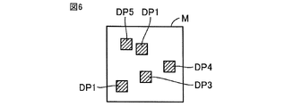
- FIG. 6 is a plan view schematically showing a logical sum of dummy patterns formed on a plurality of mask blanks.
- the hatched area in FIG. 6 is a logical sum (prohibited area) of the dummy patterns DP1 to DP5 shown in FIGS.
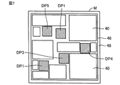
- FIG. 7 is a plan view schematically showing an example of a floor plan.
- FIG. 7 shows an example in which various functional modules 40 are arranged avoiding the prohibited area (logical sum of dummy patterns DP1 to DP5) shown in FIG.
- a dicing area 48 is provided surrounding the chip area 46 where the functional module 40 is disposed.
- FIG. 8 is a plan view schematically showing an example of placement and routing.
- FIG. 8 shows an example in which the wiring pattern 42 is generated avoiding the prohibited area (logical sum of the dummy patterns DP1 to DP5) in the example of the floor plan of FIG.
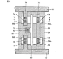
- FIG. 9 is a plan view schematically showing a circuit pattern of an inverter as an example of a functional module.
- 10 is a cross-sectional view taken along line XX of FIG. 9 and 10, a region 80 corresponds to a functional module range.
- Mask I An N-type well region 52 is defined on the P-type semiconductor substrate 50.
- Mask II Defines the STI region 54.
- Mask III Defines the regions of the P + diffusion layers 56A and 56B.
- Mask IV N + diffusion layers 58A and 58B are defined.
- Mask V Defines regions of the gate oxide film 62 and the gate electrode 60.
- Mask VI Contacts 74, 76, 78 and 82 are defined in the insulating film 64.
- Mask VII Defines first metal wirings 66, 68, 70, 72. Of the above masks, at least masks II, V, VI, and VII are formed as masks for the EUV exposure apparatus. Therefore, it is desirable that a semiconductor integrated circuit device can be manufactured even if these masks contain defects.
- FIG. 11 is a plan view schematically showing a mask layout for forming the gate electrode of FIG.
- the defect DP2 is included in the pattern of the Ta layer (absorption layer).
- the entire pattern to be drawn on the mask V is moved.
- the gate electrode pattern 84 is formed of a Ta layer
- the position of the entire pattern is shifted so that the defect DP2 is located inside the gate electrode pattern 84.
- it becomes difficult to arrange the entire pattern so as to avoid defects as the number of defects included in the mask blank increases.
- the functional module arrangement area 86 is arranged such that the defect DF2 (more specifically, the dummy pattern DP2 covering the defect DF2) is located outside the functional module arrangement area 86. Is determined. That is, in the prior art, the arrangement of the pattern on the mask blank was finely corrected at the stage of mask drawing S125 in FIG. 1, whereas in the case of the first embodiment, a defect was detected at the stage of layout design S115. Placement and routing are performed in consideration of information. In this respect, the layout design method according to the first embodiment is greatly different from the prior art.
- the functional module includes a plurality of transistors each including a gate electrode wiring, one or more metal wiring layers above the gate electrode, and contacts connecting the plurality of transistors and the metal wiring layer.
- a part of the wiring pattern inside the functional module must not be changed so as to avoid defects.
- the shape of the gate electrode pattern 84 should not be changed. This is because if it is changed, a new pattern verification is required.
- a region including an uncorrectable defect remaining on the mask blank is set as a dummy pattern or an unused PIN region. Use as a module and wiring area is prohibited. Since automatic placement and routing is performed under such constraints, even mask blanks having defects can be used for LSI manufacturing. As a result, the manufacturing cost of the mask is reduced, the delivery time of the mask is shortened, and resources are not wasted.
- the pattern layout of the second metal wiring layer M2 immediately above the mask blanks is somewhat limited.
- the pattern layout of the upper metal wiring layer is not affected by the defect of the first metal wiring layer M1. If the wiring does not constitute a functional module, wiring that overlaps the prohibited area in plan view using the upper metal wiring layer may be formed on the pattern layout. If there is no restriction on the pattern layout, a wiring that overlaps the prohibited area may be formed in a plan view using the second metal wiring layer.
- FIG. 12 is a flowchart showing a layout design procedure in the semiconductor integrated circuit layout design method according to the second embodiment.
- the flowchart of FIG. 12 differs from the flowchart of FIG. 5 in the case of Embodiment 1 in that step S310A is executed instead of step S310.
- a dummy pattern is often arranged around a resistance element, an inductance element, a capacitance element, etc., in order to increase the pattern accuracy of these elements. Since the dummy pattern provided in such an analog circuit is irrelevant to the actual circuit operation, a mask blank defect may overlap at this position. Therefore, in step S310A of FIG. 12, the dummy pattern portion of the analog circuit is allowed to overlap with the defect when arranging a plurality of functional modules.
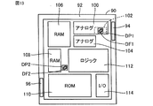
- FIG. 13 is a cross-sectional view schematically showing an example of a floor plan in the case of the second embodiment.
- analog circuits 100 and 104, RAMs 106 and 108, ROM 110, logic circuit 112, and I / O circuit 114 are arranged as functional modules.
- a dicing (scribe line) region 92 is provided around the chip region.
- TEG (Test Element Group) patterns 94 and 96 are provided in the dicing area 92.
- the TEG patterns 94 and 96 include various patterns such as alignment marks, overlay marks, and TEGs for various device evaluations.
- dummy patterns DP1 and DP2 are set to cover the defects DF1 and DF2, respectively.
- Each functional module is arranged so as to avoid the dummy pattern DP2.
- the dummy pattern DP1 covering the defect DF1 is arranged on the dummy pattern region 102 provided in the analog circuit 100.
- the functional module having a dummy pattern is not limited to an analog circuit, and a defective portion on the mask may be allowed to be disposed in the dummy pattern region.
- the defective part on the mask should be placed in that area. It may be acceptable.
- mask blanks having defects remaining can be used for manufacturing LSIs as in the first embodiment.
- the manufacturing cost of the mask is reduced, the delivery time of the mask is shortened, and resources are not wasted.
- FIG. 14 is a flowchart showing a layout design procedure in the layout design method for a semiconductor integrated circuit according to the third embodiment.
- the flowchart of FIG. 14 differs from the flowchart of FIG. 5 in the case of Embodiment 1 in that it further includes step S315.
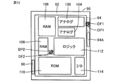
- FIG. 15 is a cross-sectional view schematically showing an example of a floor plan in the case of the third embodiment.
- the third embodiment shown in FIG. 15 differs from the case shown in FIG. 14 in that the defect DF1 overlaps the scribe line region (dicing region) 92.
- the placement and routing tool places each functional module 100, 104, 106, 108, 110, 112, 114 and the TEG patterns 94, 96 under the constraint that the dummy pattern DP1 covering the defect DF1 is avoided. Connect the functional modules together.
Landscapes
- Physics & Mathematics (AREA)
- Engineering & Computer Science (AREA)
- General Physics & Mathematics (AREA)
- Theoretical Computer Science (AREA)
- Computer Hardware Design (AREA)
- Evolutionary Computation (AREA)
- Geometry (AREA)
- General Engineering & Computer Science (AREA)
- Design And Manufacture Of Integrated Circuits (AREA)
Abstract
一実施の形態による半導体集積回路のレイアウト設計方法では、マスクブランク(M1~M5)の欠陥情報(DF1~DF5)に基づいて禁止領域(DP1~DP5)が設定される。配置配線ツールは、設定された禁止領域を避けて複数の機能モジュール(40)を配置し、禁止領域を避けて複数の機能モジュール間の配線パターン(42)を生成する。
Description
この発明は、半導体集積回路のレイアウト設計方法および装置に関し、たとえば、EUV(Extreme Ultra-Violet)マスク用のパターンレイアウトを作製する際に好適に用いられるものである。
LSI(Large Scaled Integration)用のマスク製造では、マスクブランクには欠陥が全くないことを前提としている。しかし、実際には光露光用のマスクブランク(反射防止膜を含めてもせいぜい2-3層の構造)の場合でも、欠陥の発生確率はなかなか0にはならず、数%の確率で欠陥が発生している。もし欠陥が発生したら、洗浄または修正を試みるが、それでも、修正しきれない場合は、マスクブランクの再作製にならざるを得ない。
EUV露光用のマスクブランクの場合はさらに深刻である。EUV用マスクブランクでは、40-60層の多層膜による反射を利用している。したがって、EUV露光用のマスクブランクは、光露光用のマスクブランクに比べて欠陥の発生する確率はかなり大きい。さらに、発生した欠陥を修正するのも至難の業である。具体的に、マスクブランクの修正のためには、一旦多層膜をはがし、異物を取り除いてから再び多層膜を形成することになる。この場合、修正の有無で多層膜の反射率および位相に有意差があってはならないし、修正部分と無修正部分との境界に不整合があってはならない。このように、修正にかかる手間およびコストを勘案すると、EUV露光用のマスクブランクスの欠陥を修正するのは、事実上不可能である。
そこで、欠陥のあるマスクブランクスを利用してマスク作製を行う方法が、複数の文献(特許文献1~4)で提案されている。これらの文献の方法は、マスクブランクに対して、欠陥の種類及び欠陥の座標等を含む欠陥情報が付与される点で共通している。
ここで、EUV用のマスクは、反射層としてのMo/Si(モリブデン/シリコン)多層膜、SiO2(二酸化珪素)膜、および遮光を行う吸収層としてのTa(タンタル)膜が基板上に積層された構成を有し、Ta膜がパターン状に加工される。欠陥個所を吸収層であるTa膜のパターンに重ねることによって、欠陥の影響が除去される。
具体的に、欠陥箇所をTa膜のパターンに重ねるために、特開2010-008738号公報(特許文献1)に記載の方法では、マスクブランクの主表面と平行な面内でマスクブランクを回転させる。特開2010-219445号公報(特許文献2)、特開2001-033941号公報(特許文献3)、および特開2004-170948号公報(特許文献4)に記載の方法では、回路パターンをマスクブランクの面内方向で移動したり、面内で回転したり、回路パターンの倍率を変更したりする。
マスクブランク上に形成する回路パターンの位置は、露光装置の制約のためにほぼ決まっており、マスクブランク上での回路パターンの配置の自由度は大きくない。このため、EUV露光用のマスクのように欠陥の数が比較的多くなる場合には、上記の文献に記載の方法で全ての欠陥箇所を避けるように回路パターンを形成することは困難である。結果として、フォトマスクを再作製することになると、コストが増加し、納期が遅延し、資源を浪費する等の問題が生じる。
その他の課題と新規な特徴は、本明細書の記述および添付図面から明らかになるであろう。
一実施の形態による半導体集積回路のレイアウト設計方法では、マスクブランクの欠陥情報に基づいて禁止領域が設定される。配置配線ツールは、設定された禁止領域を避けて複数の機能モジュールを配置し、禁止領域を避けて複数の機能モジュール間の配線パターンを生成する。
上記の実施の形態によれば、欠陥を含むマスクを用いて半導体集積回路装置を製造することが可能になる。
以下、各実施の形態について図面を参照して詳しく説明する。なお、同一または相当する部分には同一の参照符号を付して、その説明を繰返さない。
<実施の形態1>
図1は、実施の形態1によるレイアウト設計方法を含む、半導体集積回路用のマスク作製手順を示すフローチャートである。図1のフローチャートは、たとえば、半導体素子、液晶表示素子、および撮像素子(CCD:Charge-Coupled Device)などの半導体集積回路装置を製造する際、または薄膜磁気ヘッドなどのマイクロデバイスを製造する際に必要なマスク作製手順に関するものである。
図1は、実施の形態1によるレイアウト設計方法を含む、半導体集積回路用のマスク作製手順を示すフローチャートである。図1のフローチャートは、たとえば、半導体素子、液晶表示素子、および撮像素子(CCD:Charge-Coupled Device)などの半導体集積回路装置を製造する際、または薄膜磁気ヘッドなどのマイクロデバイスを製造する際に必要なマスク作製手順に関するものである。
半導体集積回路装置のレイアウトパターンの設計では、図1のように、RTL(Register Transfer Level)で記述された製品仕様S100に基づき、例えばCAD(Computer Aided Design)等のコンピュータシステムを用いて、論理設計(論理合成)S105、論理検証S110、レイアウト設計S115、およびレイアウト検証S120の順で設計が進行していく。
ネットリストDT10は、HDL(ハードウェア記述言語:Hardware Description Language)で記述されたデジタル回路を論理合成することによって作成される。このネットリスト情報に従い,ゲートおよびネット(接続)をFPGA(Field-Programmable Gate Array)の論理ブロックおよびI/O(Input/Output)ピンに割り当てる作業を配置配線という。この配置配線の作業は,FPGA開発ツールが自動的に行う。FPGA開発ツールに対してタイミング制約や回路面積の制約を与えることで,ある程度その制約に合わせた配置配線を実現できる。
上記のHDLとは、ハードウェアの動作と接続とを記述するプログラミング言語のことである。デジタル回路設計ではハードウェア記述言語による設計入力が主流となっており、Verilog HDLとVHDLとが業界標準として広く普及している。VHDLは、米国国防総省の納入仕様書を原点としており、VHSIC(Very High Speed Integrated Circuits) Hardware Description Language を略してVHDLとなり、後にIEEE1076として規格された。Verilog HDLは、民間企業の商用シミュレーション・ツール用の言語として誕生し、その後IEEE1364として規格化されている。Verilog HDLもVHDLも抽象度の高い記述から部品の接続のような構造的な記述まで対応できる言語である。製品仕様をRTLのスタイルで記述することにより、論理合成ツールを用いて製品仕様をゲート・レベルのネットリストへ変換可能である。さらに、シミュレーション・ツールを使って、記述されたモデルの動作確認を行なうことができる。シミュレーションで使用するテストベンチもHDLで記述する。
セルライブラリDT12は、レイアウト設計済みのマクロセル(機能モジュール)を多数集めたデータベースのことである。セルライブラリDT12には、論理機能、電気特性、およびパターンレイアウトなど、LSI(Large Scale Integration)の設計に必要なデータが格納されている。機能モジュールは、たとえば、ADC(Analog-to-Digital Converter)、DAC(Digital-to-Analog Converter)、およびPLL(Phase Locked Loop)などのアナログ回路、SRAMおよびフラッシュメモリなどのメモリ回路、インバータ、容量素子、抵抗素子、コイル、I/O回路など多岐にわたる。セルライブラリDT12は、論理設計S105およびレイアウト設計S115で用いられる。
レイアウト設計S115では、セルライブラリDT12の情報とネットリストDT10とに基づいて、自動配置配線ツールを用いて、チップ上のセルおよびマクロセルの配置を決定し(フロアプラン)、複数のセルおよび複数のマクロセルの相互の間を配線する。これによって、フォトマスク上のレイアウトパターンDT16が得られる。
最近の半導体集積回路製品には、様々な機能が盛り込まれているので、人手での配置配線は不可能なほど回路規模が大きくなっている。このため、自動配置配線ツールが用いられる。配置配線ツールは、各種機能モジュールを配置し、配置した各種機能モジュール同士を配線して、半導体集積回路製品を設計していく。このとき、チップ面積の縮小と、信号のタイミングを合わせることとが特に重要である。配置配線ツールでは、信号のタイミングが合わないときには、タイミングを調整するために冗長なインバータを挿入することもある。しかし、このような冗長回路が増えるとチップ面積が増えてしまうので、チップ面積の縮小と信号のタイミングの整合との最適化が行われる。なお、配置配線ツールは、半導体集積回路の設計を実現するコンピュータプログラムを指し、又は、コンピュータにプログラムがインストールされ半導体集積回路を設計可能な状態にあるコンピュータシステムをも指す。
FPGAの設計では、設計者の期待値通りの動作が実現するように、論理合成S105およびレイアウト設計S115を行う前に、いくつかの制約条件を開発ツールに入力しておく必要がある。設計の手戻りを少なくし、チップの開発期間を短縮し、無駄なチップコストおよび開発コストを発生させないためには、制約設定を正しく行うことが重要である。制約を設定するには、開発ツールに付属したウィザードを利用したり、テキストファイルに直接記述してインポートしたりする。制約設定が正しく行われていれば、最終的に開発ツールが、設定された制約を満たすように、チップの回路構成を自動的に最適化する。
ここで、実施の形態1による半導体集積回路装置のパターンレイアウトの設計方法では、マスクブランクスの欠陥情報が制約条件として利用される点に特徴がある。欠陥情報とは、マスクブランク上に存在する、洗浄または修正によって除去できない欠陥の位置および大きさなどの情報をいう。
具体的に、本実施の形態によるレイアウト設計方法では、マスクブランクに欠陥があった場合、その欠陥を覆うようにフラグ図形(ダミーパターン)を発生させる。フラグ図形の大きさは、露光装置の最小解像度以上という条件を満たしたうえで、欠陥を覆うのに必要最小限の大きさに設定される。フラグ図形の形状は、矩形または円形など特に限定されない。発生したフラグ図形は、マスクブランクに付随する情報としてGDSまたはOASISなどの標準形式で、欠陥情報ライブラリDT14に保存される。GUI(Graphical User Interface)を利用しない場合は、フラグ図形を保存する形式としてCSV形式を利用してもよい。フラグ図形の情報は、レイアウト設計時に、欠陥情報ライブラリDT14からレイアウト設計用の配置配線ツールへ配置制約条件として出力される。これによって、配置配線ツールは、フラグ図形を避けて機能モジュールを配置したり、フラグ図形を避けてモジュール同士を結線したりできる。フラグ図形はすなわち欠陥であるから、マスクブランクスの欠陥を避けて集積回路製品を設計することができる。
マスクレイアウトパターンの設計データが完成すると、設計データを用いてマスク描画を行うことにより、マスクが製造される(ステップS125)。電子ビーム(EB)またはレーザービームを用いた描画装置で描画することにより、複数のパターンを有するマスクが形成される。フォトマスクとしては、光露光用の透過型マスクに加えて、最近では、EUV露光用の多層膜反射マスクが実用化されようとしている。
完成したマスクは、半導体集積回路製品の製造に使用される。紫外線(UV光)またはEUV光を用いた投影光学系により半導体基板上に集積回路パターンが一括露光される。すなわち、フォトマスクのパターン像は、フォトレジストが塗布されたウエハおよびガラスプレート等の上に投影される。さらに、このような操作を繰り返すことによって、素子分離構造、ウェル、拡散領域、ゲート電極層、および多層配線層などが順次形成され、半導体集積回路装置が完成する。
図2は、マスクブランクに付随する欠陥情報の作成手順を示すフローチャートである。図2を参照して、最初に、マスクブランクが作成される(ステップS200)。光マスクの場合は、透明基板の1主面上に遮光膜が形成される。要求精度に応じて、表面に反射防止膜を形成する場合がある。EUVマスクの場合は、基板の1主面上にSiとMoとによる40-60層の多層反射膜が形成され、さらにその上にSiO2膜が形成され、さらにその上に吸収層としてのTa膜が形成される。
次に、マスク表面に付着した異物を除去するために、マスクブランクが洗浄される(ステップS205)。続いて、マスクブランク上の欠陥が検査される(ステップS210)。欠陥検査の手法としては、散乱光を利用する方法、die-by-die、およびdie-to-databaseといった公知の手法がある。
修正可能な欠陥がある場合は(ステップS215でNO、ステップS220でYES)、欠陥の修正を試みた上で(ステップS225)、再び、マスクブランク上の欠陥が検査される(ステップS210)。
一方、修正不可能な欠陥の場合には(ステップS220でNO)、欠陥の位置と大きさとが計測される。欠陥の位置は、マスクブランク上の基準(fiducial)マークの位置を基準にして測定される。そして、欠陥を覆う最小の領域に認識レイヤでダミーパターン(フラグ図形)が生成される(ステップS235)。生成したダミーパターンは、マスクブランクに対応付けて欠陥情報ライブラリDT14に格納される(ステップS240)。
図3は、マスクブランク上の欠陥およびそれを覆うダミーパターンの例を模式的に示す平面図である。図3では、説明を簡略化するために、各マスクに1個ずつ欠陥が発生した場合が示されているが、実際には、欠陥は1枚のマスクに複数発生する場合もあるし、無欠陥が実現できる場合もある。さらに、図3では、図解を容易にするために欠陥を実際よいも大きく記載しているが、実際の欠陥の大きさは、大きくても数μm程度である。
図3の例では、特にパターン精度が必要なSTI(Shallow Trench Isolation)層、ゲート電極層、コンタクト層、および第1金属配線層(M1)のマスクM1~M4について、EUV露光が行われる。これらの主要なマスクM1~M4と予備のマスクM5とについて、図3に示すように欠陥DF1~DF5が見つかったとする。この場合、欠陥を覆う最小の領域に認識レイヤでダミーパターンDP1~DP5がそれぞれ生成される。生成したダミーパターンは対応するマスクブランクに対応付けて図1の欠陥情報ライブラリDT14に格納される。欠陥情報とともにマスクブランクがストックされる。
なお、新製品では、将来的にマスク改訂することも有りうるので、予備用のマスクブランクスについても欠陥情報をライブラリに格納して、必要な枚数のマスクブランクスをストックしておくのが好ましい。
なお、改訂対象となったマスクは、一旦マスクパターン(光マスクの場合の遮光膜、ならびにEUVマスクの場合の多層反射膜および吸収膜)を剥離し、再び遮光膜または多層反射膜を形成することによりマスクブランクスを形成するのが好ましい。修正不可能な欠陥がなくなることもあるし、同じ位置に欠陥が再現したとしても、同じマスクセットの次のマスク改訂用に使用することができる。もし、修正不可能な欠陥が別の位置に発生してしまった場合には、同じマスクセット用には使えないが、その欠陥の位置や大きさを計測することで、次のマスクセット用になら使うことができる。
図4は、実施の形態1による半導体集積回路のレイアウト設計方法を具現化するためのコンピュータシステムの構成図である。
一般に、半導体集積回路の設計には、汎用のコンピュータシステムが用いられる。図4を参照して、コンピュータシステム10は、1つ以上のプロセッサ(CPU:Central Processing Unit)12と、RAM(Random Access Memory)14と、ROM(Read Only Memory)16とを含む。ROM16はコンピュータの基本的な操作システムを格納し、RAM14はプロセッサ12での現時点の処理に必要なアプリケーションおよびプログラムなどを格納する。
プロセッサで処理されるデータは、システムバス34を介して、ポートアダプタ18およびI/Oアダプタ22などから入力される。たとえば、設計用のプログラムおよび加工対象のデータは、大容量記憶装置(ハードディスクなど)またはリムーバル記憶装置(磁気ディスク、光ディスク、フレキシブルディスクなど)24からI/Oアダプタ22を介して入力されたり、ポートアダプタ18を介してデータポート20から入力されたりする。ここで加工対象のデータとは、図1のネットリストDT10、セルライブラリDT12、欠陥情報ライブラリDT14、レイアウトパターンDT16などである。
ユーザは、ユーザインターフェースアダプタ26を介してマウスおよびキーボードなどによる操作を行う。プロセッサ12による処理結果は、ディスプレーアダプタ30を介して、CRT(Cathode Ray Tube)または液晶ディスプレーなどの表示デバイス32に表示される。
図5は、図1のレイアウト設計の手順の詳細を示すフローチャートである。図5に示す各手順は、図4のプロセッサ12で配置配線ツール等のプログラムが実行されることに実現される。
まず、プロセッサ12は、予備を含めて必要な複数枚のマスクブランクスに対応する欠陥情報を図1の欠陥情報ライブラリDT14から取得する(ステップS300)。予備マスクを含める理由は、マスク改訂の場合は予備マスクを使うことになるため、予備マスクの欠陥情報も考慮して配置配線を行う必要があるからである。
次に、プロセッサ12は、取得した欠陥情報として記憶されている複数のダミーパターンの論理和(以下、「禁止領域」と称する)を生成する(ステップS305)。プロセッサ12は、生成した禁止領域を配置配線ツールで読み取れるフォーマットで出力する。具体的には、GDS2やOASIS等の標準フォーマットで出力するのが好ましい。もしくは、CSV形式で禁止領域を出力してもよい。
次に、配置配線ツールでの処理に移る。配置配線ツールにおいて、プロセッサ12は、上記の禁止領域を読み込み、この禁止領域を配置制約事項としたり、未使用ピン(PIN)として設定したりする。これによって、配置配線ツールは、禁止領域を避けて機能モジュールの位置を微調整して配置したり(ステップS310)、禁止領域を避けて機能モジュール間の配線を行ったり(ステップS320)することができる。
以下、「ピン・アサイン」の制約について説明する。ピン・アサインとは、ハードウェア的に接続されるように、FPGAのピン番号と回路図上のピンとを正しく対応させることをいう。但し、単にピン同士を電気的に接続するだけでは、信号品質(シグナルインテグリティ)および/またはタイミングの問題が実機上で生じることがある。さらには、配線層の増加または再設計によってプリント基板のコストアップの要因になることがあるので注意が必要である。
プリント基板上でFPGAを正しく動作させるためには、ピンの割り当てを行う際に、プリント基板上の回路設計および電子部品の実装も考慮しなければならない。クロックピンおよびディファレンシャルピンの配置といったI/Oピンの構造、内部のセル構造などに関連するチップ固有の制約については、データシートで確認することによりピン・アサインの制約を正確に行うことが重要である。プリント基板上におけるFPGAの配置と、その配線の要件を満たしたピン・アサインを作成することによって、FPGA設計者、プリント基板設計者およびハードウェア設計者の間で発生する手戻りを少なくすることができ、その結果、設計のコスト削減および設計期間の短縮が実現できる。
市販ツールであるアルテラ社のQuartus IIではピン情報の編集を行うために可視化ツール「Pin Planner(ピン・プランナ)」が搭載されている。この機能を使用することにより、作成した回路(デザイン)の入力ピン、出力ピンおよび双方向ピンを、FPGAの目的のピンに割り当てることができる。このPin PlannerはGUIを使用して、ドラッグ&ドロップなどグラフィカルにピンの設定が行える。さらに、Pin Plannerではピンの割り当てだけではなく、ピンのI/O規格の設定および未使用ピンの処理方法なども設定することができる。
Quartus II ではGUIでの操作に加えて、CSV(カンマ区切り)ファイルを使用した設定も可能である。CSVファイルを編集する際の表記については、決められたフォーマットで記述する必要がある。
例えば、ピン番号を変更する場合は、Location欄のピン番号を編集する。記述例は以下のようになる。
記述 : PIN_番号
記述例 : PIN_E2
I/O規格を変更する場合は、I/O Standard欄の規格名を編集する。記述は以下の通りである。
記述例 : PIN_E2
I/O規格を変更する場合は、I/O Standard欄の規格名を編集する。記述は以下の通りである。
記述例 : 3.3V LVTTL
このように、Quartus IIを用いてピン・アサイン制約を設定する方法としては、GUIベースの“Pin Planner”と、“CSV”ベースの方法との2つのインポート方法がある。このため、設計者は使用するチップの種類、作業効率、設計の熟練度などに応じて、設定しやすい方法でピン・アサインを行うことができる。
このように、Quartus IIを用いてピン・アサイン制約を設定する方法としては、GUIベースの“Pin Planner”と、“CSV”ベースの方法との2つのインポート方法がある。このため、設計者は使用するチップの種類、作業効率、設計の熟練度などに応じて、設定しやすい方法でピン・アサインを行うことができる。
図6は、複数のマスクブランクス上に形成されたダミーパターンの論理和を模式的に示す平面図である。図6でハッチング付した領域は、図3(A)~(E)に示したダミーパターンDP1~DP5の論理和(禁止領域)である。
図7は、フロアプランの一例を模式的に示す平面図である。図7では、図6で示した禁止領域(ダミーパターンDP1~DP5の論理和)を避けて各種機能モジュール40が配置されている例が示されている。機能モジュール40が配置されるチップ領域46を取り囲んでダイシング領域48が設けられる。
図8は、配置配線の例を模式的に示す平面図である。図8では、図7のフロアプランの例において、禁止領域(ダミーパターンDP1~DP5の論理和)を避けて配線パターン42が生成される例が示されている。
図9は、機能モジュールの一例としてインバータの回路パターンを模式的に示す平面図である。図10は、図9のX-X線に沿う断面図である。図9および図10において、領域80が機能モジュールの範囲に相当する。
図9および図10に示すインバータを形成するためには、以下のマスクI~VIIが少なくとも必要である。
マスクI:P型半導体基板50上にN型ウェル領域52を規定する。
マスクII:STI領域54を規定する。
マスクII:STI領域54を規定する。
マスクIII:P+拡散層56A,56Bの領域を規定する。
マスクIV:N+拡散層58A,58Bの領域を規定する。
マスクIV:N+拡散層58A,58Bの領域を規定する。
マスクV:ゲート酸化膜62およびゲート電極60の領域を規定する。
マスクVI:絶縁膜64中にコンタクト74,76,78,82を規定する。
マスクVI:絶縁膜64中にコンタクト74,76,78,82を規定する。
マスクVII:第1の金属配線66,68,70,72を規定する。
以上のマスクのうち、少なくともマスクII,V,VI,VIIを、EUV露光装置用のマスクとして形成するものとする。したがって、これらのマスクに欠陥が含まれていても半導体集積回路装置が製造可能であることが望ましい。
以上のマスクのうち、少なくともマスクII,V,VI,VIIを、EUV露光装置用のマスクとして形成するものとする。したがって、これらのマスクに欠陥が含まれていても半導体集積回路装置が製造可能であることが望ましい。
図11は、図9のゲート電極を形成するためのマスクレイアウトを模式的に示す平面図である。
図11を参照して、従来技術では、ゲート電極パターン84を規定するためのマスクVに欠陥DP2が含まれている場合、その欠陥DP2がTa層(吸収層)のパターンに含まれるように、マスクVに描画するパターン全体を移動させていた。たとえば、ゲート電極パターン84がTa層で形成される場合には、ゲート電極パターン84の内部に欠陥DP2が位置するようにパターン全体の位置がシフトされる。このため、マスクブランクに含まれる欠陥が増加するにつれて欠陥を避けるようにパターン全体を配置することが困難になってしまう。
一方、実施の形態1によるレイアウト設計方法によれば、欠陥DF2(より詳しくは、欠陥DF2を覆うダミーパターンDP2)が機能モジュールの配置領域86の外に位置するように、機能モジュールの配置領域86が決定される。すなわち、従来技術では、図1のマスク描画S125の段階でマスクブランク上でのパターンの配置が微修正されていたのに対して、実施の形態1の場合には、レイアウト設計S115の段階で欠陥情報を考慮して配置配線が行われる。この点で、実施の形態1によるレイアウト設計方法は、従来技術と大きく異なる。
機能モジュールは、一例として、各々ゲート電極配線を含む複数のトランジスタ、ゲート電極よりも上層の1または複数の金属配線層、およびこれら複数のトランジスタと金属配線層との間を接続するコンタクトで構成される。機能モジュールを構成する配線の配線パターンは検証済みであるので、機能モジュールの内部の配線パターンの一部を、欠陥を避けるように変更してはならない。たとえば、図11の場合には、ゲート電極パターン84の形状自体を変更してはならない。もし、変更した場合には、新たにパターン検証が必要になってしまうからである。そして、機能モジュールのある配線パターンを形成するための1つのマスクに欠陥があるがその他の配線の配線パターンを形成するための1または複数のマスクに欠陥がないとしても、機能モジュール全体で(すなわち、全てのマスクで)その欠陥を避けて当該機能モジュールを配置する。
以上説明したように、実施の形態1による半導体集積回路のレイアウト設計方法によれば、マスクブランクス上に残った修正不可能な欠陥を含む領域を、ダミーパターンまたは未使用PIN領域に設定し、機能モジュールおよび配線領域として使用することを禁止する。このような制約条件の下に自動配置配線を行うので、欠陥の存在するマスクブランクスでもLSIの製造に使用することができる。この結果、マスクの製造コストが低減し、マスクの納期が短縮し、資源の浪費がなくなるという効果を奏する。
なお、上記の例において、第1金属配線層M1のマスクブランクスに欠陥がある場合、その直上の第2金属配線層M2のパターンレイアウトは多少制限を受ける。しかしながら、それよりもさらに上層の金属配線層のパターンレイアウトについては、第1金属配線層M1の欠陥の影響を受けることはない。機能モジュールを構成しない配線であれば、その上層の金属配線層を使用する平面視して禁止領域に重なる配線をパターンレイアウト上に形成してもよい。パターンレイアウトの制限を受けなければ、第2の金属配線層を使用する平面視して禁止領域に重なる配線を形成してもよい。
なお、上記の例では、EUV露光用のマスクに欠陥がある場合について説明したが、上記のレイアウト設計方法は通常の光露光の場合にも適用可能である。
<実施の形態2>
図12は、実施の形態2による半導体集積回路のレイアウト設計方法において、レイアウト設計の手順を示すフローチャートである。図12のフローチャートは、ステップS310に代えてステップS310Aが実行される点で、実施の形態1の場合の図5のフローチャートと異なる。
図12は、実施の形態2による半導体集積回路のレイアウト設計方法において、レイアウト設計の手順を示すフローチャートである。図12のフローチャートは、ステップS310に代えてステップS310Aが実行される点で、実施の形態1の場合の図5のフローチャートと異なる。
アナログ回路のパターンレイアウトでは、たとえば、抵抗素子、インダクタンス素子、容量素子などの周辺には、これらの素子のパターン精度を高めるためにダミーパターンが配置されることが多い。このようなアナログ回路に設けられるダミーパターンは実際の回路動作とは無関係であるので、この位置にマスクブランクスの欠陥が重なっていても構わない。そこで、図12のステップS310Aでは、複数の機能モジュールの配置の際に、アナログ回路のダミーパターンの部分が欠陥と重なることが許容される。
図12のその他の点は図5の場合と同じであるので同一または相当するステップには同一の参照符号を付して説明を繰り返さない。
図13は、実施の形態2の場合において、フロアプランの一例を模式的に示す断面図である。図13に示すフロアプランでは、機能モジュールとしてアナログ回路100,104、RAM106,108、ROM110、ロジック回路112、およびI/O回路114が配置されている。さらに、チップ領域の周辺にダイシング(スクライブライン)領域92が設けられている。ダイシング領域92には、TEG(Test Element Group)パターン94,96が設けられる。TEGパターン94,96は、アライメントマーク、重ね合わせマーク、各種デバイス評価用のTEG等、種々のパターンを含む。
図13の例では、欠陥DF1,DF2を覆うようにダミーパターンDP1,DP2がそれぞれ設定されている。各機能モジュールは、ダミーパターンDP2を避けるように配置される。一方、欠陥DF1を覆うダミーパターンDP1は、アナログ回路100に設けられているダミーパターンの領域102上に配置されている。なお、アナログ回路に限ることなく、ダミーパターンを有する機能モジュールであれば、マスク上の欠陥部分がそのダミーパターンの領域に配置されること許容してもよい。さらにはダミーパターンでなくても、機能モジュールにその機能を実現する配線パターンが形成されない領域であって欠陥部分より大きい領域がある場合には、マスク上の欠陥部分がその領域に配置することを許容してもよい。
上記のとおり、実施の形態2のレイアウト設計方法によれば、実施の形態1と同様に、欠陥の残ったマスクブランクスでもLSIの製造に使用することができる。この結果、マスクの製造コストが低減し、マスクの納期が短縮し、資源の浪費がなくなるという効果を奏する。
<実施の形態3>
図14は、実施の形態3による半導体集積回路のレイアウト設計方法において、レイアウト設計の手順を示すフローチャートである。図14のフローチャートは、ステップS315をさらに含む点で、実施の形態1の場合の図5のフローチャートと異なる。
図14は、実施の形態3による半導体集積回路のレイアウト設計方法において、レイアウト設計の手順を示すフローチャートである。図14のフローチャートは、ステップS315をさらに含む点で、実施の形態1の場合の図5のフローチャートと異なる。
図15は、実施の形態3の場合において、フロアプランの一例を模式的に示す断面図である。図15に示す実施の形態3の場合には、欠陥DF1がスクライブライン領域(ダイシング領域)92と重なっている点で図14の場合と異なる。
図14、図15を参照して、もし、スクライブライン領域92に設けられているTEGパターン94と欠陥DF1とが重なった場合には、このTEGは正常に機能しなくなる。そこで、配置配線ツールは、欠陥DF1を覆うダミーパターンDP1を避けるという制約条件のもとに、各機能モジュール100,104,106,108,110,112,114ならびにTEGパターン94,96を配置するとともに、機能モジュール同士を結線する。
上記の構成によって、実施の形態1の場合と同様に、欠陥の残ったマスクブランクスでもLSIの製造に使用することができる。この結果、マスクの製造コストが低減し、マスクの納期が短縮し、資源の浪費がなくなるという効果を奏する。なお、実施の形態2と実施の形態3とを組み合わせることも可能である。
以上、本発明者によってなされた発明を実施の形態に基づき具体的に説明したが、本発明は上記実施の形態に限定されるものではなく、その要旨を逸脱しない範囲で種々変更可能であることは言うまでもない。
10 コンピュータシステム、12 プロセッサ、40 機能モジュール、42 配線、46 チップ領域、48,92 ダイシング領域、94,96 TEGパターン、DF1~DF5 欠陥、DP1~DP5 ダミーパターン、DT10 ネットリスト、DT12 セルライブラリ、DT14 欠陥情報ライブラリ、DT16 レイアウトパターン、S100 製品仕様、S105 論理設計、S105 論理合成、S110 論理検証、S115 レイアウト設計、S120 レイアウト検証、S125 マスク描画。
Claims (7)
- マスクブランクに存在する1または複数の欠陥の位置および大きさを少なくとも示す欠陥情報を取得するステップと、
前記欠陥情報に基づいて禁止領域を設定するステップと、
前記禁止領域を避けて複数の機能モジュールを配置するステップと、
前記禁止領域を避けて前記複数の機能モジュール間を配線するステップとを備える、半導体集積回路のレイアウト設計方法。 - 前記欠陥情報を取得するステップでは、複数のマスクブランクの各々の欠陥情報を取得し、
前記設定するステップは、
前記複数のマスクブランクの各々の欠陥情報に基づいて各欠陥の覆うようにダミーパターンを生成するステップと、
生成した複数の前記ダミーパターンの論理和に基づいて禁止領域を設定するステップとを含む、請求項1に記載の半導体集積回路のレイアウト設計方法。 - 前記設定するステップは、前記禁止領域としてダミーパターンまたは未使用ピンを設定するステップを含む、請求項1に記載の半導体集積回路のレイアウト設計方法。
- 前記欠陥情報は、EUV(Extreme Ultra-Violet)露光用のマスクブランクを検査して得られたものである、請求項1に記載の半導体集積回路のレイアウト設計方法。
- 前記複数の機能モジュールは、ダミーパターンを有するアナログ回路を含み、
前記配置するステップは、前記アナログ回路のダミーパターンに前記禁止領域を設けることを許容する、請求項1に記載の半導体集積回路のレイアウト設計方法。 - スクライブライン領域に設けられるTEG(Test Element Group)パターンを、前記禁止領域を避けて配置するステップをさらに備える、請求項1に記載の半導体集積回路のレイアウト設計方法。
- マスクブランクに存在する1または複数の欠陥の位置および大きさを少なくとも示す欠陥情報を格納するデータベースと、
プロセッサとを備え、
前記プロセッサは、
前記欠陥情報に基づいて禁止領域を設定し、
前記禁止領域を避けて複数の機能モジュールを配置し、
前記禁止領域を避けて前記複数の機能モジュール間を配線するように構成される、半導体集積回路のレイアウト設計装置。
Priority Applications (1)
| Application Number | Priority Date | Filing Date | Title |
|---|---|---|---|
| PCT/JP2014/062054 WO2015166570A1 (ja) | 2014-05-01 | 2014-05-01 | 半導体集積回路のレイアウト設計方法および装置 |
Applications Claiming Priority (1)
| Application Number | Priority Date | Filing Date | Title |
|---|---|---|---|
| PCT/JP2014/062054 WO2015166570A1 (ja) | 2014-05-01 | 2014-05-01 | 半導体集積回路のレイアウト設計方法および装置 |
Publications (1)
| Publication Number | Publication Date |
|---|---|
| WO2015166570A1 true WO2015166570A1 (ja) | 2015-11-05 |
Family
ID=54358321
Family Applications (1)
| Application Number | Title | Priority Date | Filing Date |
|---|---|---|---|
| PCT/JP2014/062054 Ceased WO2015166570A1 (ja) | 2014-05-01 | 2014-05-01 | 半導体集積回路のレイアウト設計方法および装置 |
Country Status (1)
| Country | Link |
|---|---|
| WO (1) | WO2015166570A1 (ja) |
Citations (6)
| Publication number | Priority date | Publication date | Assignee | Title |
|---|---|---|---|---|
| JP2003149793A (ja) * | 2001-11-13 | 2003-05-21 | Toshiba Corp | マスクブランクスの選択方法、露光マスクの形成方法、および半導体装置の製造方法 |
| JP2007140128A (ja) * | 2005-11-18 | 2007-06-07 | Dainippon Printing Co Ltd | 基板選択装置 |
| JP2010079112A (ja) * | 2008-09-28 | 2010-04-08 | Hoya Corp | フォトマスクの製造方法、及びパターン転写方法 |
| JP2012064770A (ja) * | 2010-09-16 | 2012-03-29 | Renesas Electronics Corp | Euvl用マスクの製造方法および半導体装置の製造方法 |
| JP2012089580A (ja) * | 2010-10-15 | 2012-05-10 | Renesas Electronics Corp | Euvl用マスクの製造方法および半導体装置の製造方法 |
| JP2014039038A (ja) * | 2012-08-20 | 2014-02-27 | Commissariat A L'energie Atomique Et Aux Energies Alternatives | 基板の欠陥の影響を最小化するeuvマスクの製作方法 |
-
2014
- 2014-05-01 WO PCT/JP2014/062054 patent/WO2015166570A1/ja not_active Ceased
Patent Citations (6)
| Publication number | Priority date | Publication date | Assignee | Title |
|---|---|---|---|---|
| JP2003149793A (ja) * | 2001-11-13 | 2003-05-21 | Toshiba Corp | マスクブランクスの選択方法、露光マスクの形成方法、および半導体装置の製造方法 |
| JP2007140128A (ja) * | 2005-11-18 | 2007-06-07 | Dainippon Printing Co Ltd | 基板選択装置 |
| JP2010079112A (ja) * | 2008-09-28 | 2010-04-08 | Hoya Corp | フォトマスクの製造方法、及びパターン転写方法 |
| JP2012064770A (ja) * | 2010-09-16 | 2012-03-29 | Renesas Electronics Corp | Euvl用マスクの製造方法および半導体装置の製造方法 |
| JP2012089580A (ja) * | 2010-10-15 | 2012-05-10 | Renesas Electronics Corp | Euvl用マスクの製造方法および半導体装置の製造方法 |
| JP2014039038A (ja) * | 2012-08-20 | 2014-02-27 | Commissariat A L'energie Atomique Et Aux Energies Alternatives | 基板の欠陥の影響を最小化するeuvマスクの製作方法 |
Similar Documents
| Publication | Publication Date | Title |
|---|---|---|
| US8612899B2 (en) | Fast lithography compliance check for place and route optimization | |
| US8807948B2 (en) | System and method for automated real-time design checking | |
| US6340542B1 (en) | Method of manufacturing a semiconductor device, method of manufacturing a photomask, and a master mask | |
| JP5694463B2 (ja) | ダブルパターニング技術のための物理的決定性境界インターコネクト・フィーチャを生成するシステム及び方法 | |
| US20170115556A1 (en) | Mask manufacturing method and semiconductor device manufacturing method using the same | |
| TWI868271B (zh) | 用於使用帶有金屬線的胞元進行電路設計的方法和設備及相應產生的佈局 | |
| WO2005036603A2 (en) | Design-manufacturing interface via a unified model | |
| CN105488244B (zh) | 用于设计半导体装置的方法和系统 | |
| TWI899532B (zh) | 積體電路的佈局圖的修改方法及修改系統及電腦程式產品 | |
| TW200951749A (en) | Integrated circuit (IC) design method, system and program product | |
| US20240363594A1 (en) | Vertical interconnect structures with integrated circuits | |
| CN104570587A (zh) | 一种制备opc光刻掩膜版的系统及方法 | |
| KR102711618B1 (ko) | 3d 집적 회로 내의 수직 상호 연결 구조 | |
| US7263677B1 (en) | Method and apparatus for creating efficient vias between metal layers in semiconductor designs and layouts | |
| JP4794130B2 (ja) | マスクパターンデータ自動補正方法及びそのプログラム | |
| US8365105B2 (en) | Method of performing optical proximity effect corrections to photomask pattern | |
| US20230161937A1 (en) | Mask layout design method, mask and integrated circuit manufacturing methods, masks and integrated circuits | |
| US10324369B2 (en) | Methods for generating a mandrel mask | |
| WO2015166570A1 (ja) | 半導体集積回路のレイアウト設計方法および装置 | |
| TWI844148B (zh) | 半導體裝置及其製造方法 | |
| US7745067B2 (en) | Method for performing place-and-route of contacts and vias in technologies with forbidden pitch requirements | |
| US7926010B2 (en) | Method of determining defects in photomask | |
| US20080250374A1 (en) | Method of Making an Integrated Circuit | |
| US6868537B1 (en) | Method of generating an IC mask using a reduced database | |
| JP2006100619A (ja) | 半導体装置の製造方法および半導体装置 |
Legal Events
| Date | Code | Title | Description |
|---|---|---|---|
| 121 | Ep: the epo has been informed by wipo that ep was designated in this application |
Ref document number: 14891037 Country of ref document: EP Kind code of ref document: A1 |
|
| NENP | Non-entry into the national phase |
Ref country code: DE |
|
| 122 | Ep: pct application non-entry in european phase |
Ref document number: 14891037 Country of ref document: EP Kind code of ref document: A1 |
|
| NENP | Non-entry into the national phase |
Ref country code: JP |