WO2015155984A1 - Acoustic wave resonators, acoustic wave filters, antenna duplexers, modules and communication devices using the same - Google Patents
Acoustic wave resonators, acoustic wave filters, antenna duplexers, modules and communication devices using the same Download PDFInfo
- Publication number
- WO2015155984A1 WO2015155984A1 PCT/JP2015/001956 JP2015001956W WO2015155984A1 WO 2015155984 A1 WO2015155984 A1 WO 2015155984A1 JP 2015001956 W JP2015001956 W JP 2015001956W WO 2015155984 A1 WO2015155984 A1 WO 2015155984A1
- Authority
- WO
- WIPO (PCT)
- Prior art keywords
- acoustic wave
- overlapping region
- electrode fingers
- electrode
- region
- Prior art date
- Legal status (The legal status is an assumption and is not a legal conclusion. Google has not performed a legal analysis and makes no representation as to the accuracy of the status listed.)
- Ceased
Links
Images


Classifications
-
- H—ELECTRICITY
- H03—ELECTRONIC CIRCUITRY
- H03H—IMPEDANCE NETWORKS, e.g. RESONANT CIRCUITS; RESONATORS
- H03H9/00—Networks comprising electromechanical or electro-acoustic elements; Electromechanical resonators
- H03H9/02—Details
- H03H9/125—Driving means, e.g. electrodes, coils
- H03H9/145—Driving means, e.g. electrodes, coils for networks using surface acoustic waves
- H03H9/14544—Transducers of particular shape or position
- H03H9/14564—Shifted fingers transducers
-
- H—ELECTRICITY
- H03—ELECTRONIC CIRCUITRY
- H03H—IMPEDANCE NETWORKS, e.g. RESONANT CIRCUITS; RESONATORS
- H03H9/00—Networks comprising electromechanical or electro-acoustic elements; Electromechanical resonators
- H03H9/02—Details
- H03H9/02535—Details of surface acoustic wave devices
- H03H9/02637—Details concerning reflective or coupling arrays
- H03H9/02685—Grating lines having particular arrangements
- H03H9/02708—Shifted grating lines
-
- H—ELECTRICITY
- H03—ELECTRONIC CIRCUITRY
- H03H—IMPEDANCE NETWORKS, e.g. RESONANT CIRCUITS; RESONATORS
- H03H9/00—Networks comprising electromechanical or electro-acoustic elements; Electromechanical resonators
- H03H9/02—Details
- H03H9/125—Driving means, e.g. electrodes, coils
- H03H9/145—Driving means, e.g. electrodes, coils for networks using surface acoustic waves
- H03H9/14517—Means for weighting
- H03H9/1452—Means for weighting by finger overlap length, apodisation
-
- H—ELECTRICITY
- H03—ELECTRONIC CIRCUITRY
- H03H—IMPEDANCE NETWORKS, e.g. RESONANT CIRCUITS; RESONATORS
- H03H9/00—Networks comprising electromechanical or electro-acoustic elements; Electromechanical resonators
- H03H9/02—Details
- H03H9/125—Driving means, e.g. electrodes, coils
- H03H9/145—Driving means, e.g. electrodes, coils for networks using surface acoustic waves
- H03H9/14544—Transducers of particular shape or position
- H03H9/14547—Fan shaped; Tilted; Shifted; Slanted; Tapered; Arched; Stepped finger transducers
-
- H—ELECTRICITY
- H03—ELECTRONIC CIRCUITRY
- H03H—IMPEDANCE NETWORKS, e.g. RESONANT CIRCUITS; RESONATORS
- H03H9/00—Networks comprising electromechanical or electro-acoustic elements; Electromechanical resonators
- H03H9/02—Details
- H03H9/125—Driving means, e.g. electrodes, coils
- H03H9/145—Driving means, e.g. electrodes, coils for networks using surface acoustic waves
- H03H9/14544—Transducers of particular shape or position
- H03H9/1457—Transducers having different finger widths
-
- H—ELECTRICITY
- H03—ELECTRONIC CIRCUITRY
- H03H—IMPEDANCE NETWORKS, e.g. RESONANT CIRCUITS; RESONATORS
- H03H9/00—Networks comprising electromechanical or electro-acoustic elements; Electromechanical resonators
- H03H9/25—Constructional features of resonators using surface acoustic waves
-
- H—ELECTRICITY
- H03—ELECTRONIC CIRCUITRY
- H03H—IMPEDANCE NETWORKS, e.g. RESONANT CIRCUITS; RESONATORS
- H03H9/00—Networks comprising electromechanical or electro-acoustic elements; Electromechanical resonators
- H03H9/46—Filters
- H03H9/64—Filters using surface acoustic waves
-
- H—ELECTRICITY
- H03—ELECTRONIC CIRCUITRY
- H03H—IMPEDANCE NETWORKS, e.g. RESONANT CIRCUITS; RESONATORS
- H03H9/00—Networks comprising electromechanical or electro-acoustic elements; Electromechanical resonators
- H03H9/46—Filters
- H03H9/64—Filters using surface acoustic waves
- H03H9/6423—Means for obtaining a particular transfer characteristic
- H03H9/6433—Coupled resonator filters
- H03H9/6483—Ladder SAW filters
-
- H—ELECTRICITY
- H03—ELECTRONIC CIRCUITRY
- H03H—IMPEDANCE NETWORKS, e.g. RESONANT CIRCUITS; RESONATORS
- H03H9/00—Networks comprising electromechanical or electro-acoustic elements; Electromechanical resonators
- H03H9/70—Multiple-port networks for connecting several sources or loads, working on different frequencies or frequency bands, to a common load or source
- H03H9/72—Networks using surface acoustic waves
- H03H9/725—Duplexers
-
- H—ELECTRICITY
- H10—SEMICONDUCTOR DEVICES; ELECTRIC SOLID-STATE DEVICES NOT OTHERWISE PROVIDED FOR
- H10N—ELECTRIC SOLID-STATE DEVICES NOT OTHERWISE PROVIDED FOR
- H10N30/00—Piezoelectric or electrostrictive devices
- H10N30/80—Constructional details
- H10N30/87—Electrodes or interconnections, e.g. leads or terminals
-
- H—ELECTRICITY
- H03—ELECTRONIC CIRCUITRY
- H03H—IMPEDANCE NETWORKS, e.g. RESONANT CIRCUITS; RESONATORS
- H03H9/00—Networks comprising electromechanical or electro-acoustic elements; Electromechanical resonators
- H03H9/02—Details
- H03H9/125—Driving means, e.g. electrodes, coils
- H03H9/13—Driving means, e.g. electrodes, coils for networks consisting of piezoelectric or electrostrictive materials
- H03H9/132—Driving means, e.g. electrodes, coils for networks consisting of piezoelectric or electrostrictive materials characterized by a particular shape
-
- H—ELECTRICITY
- H03—ELECTRONIC CIRCUITRY
- H03H—IMPEDANCE NETWORKS, e.g. RESONANT CIRCUITS; RESONATORS
- H03H9/00—Networks comprising electromechanical or electro-acoustic elements; Electromechanical resonators
- H03H9/15—Constructional features of resonators consisting of piezoelectric or electrostrictive material
- H03H9/17—Constructional features of resonators consisting of piezoelectric or electrostrictive material having a single resonator
-
- H—ELECTRICITY
- H03—ELECTRONIC CIRCUITRY
- H03H—IMPEDANCE NETWORKS, e.g. RESONANT CIRCUITS; RESONATORS
- H03H9/00—Networks comprising electromechanical or electro-acoustic elements; Electromechanical resonators
- H03H9/15—Constructional features of resonators consisting of piezoelectric or electrostrictive material
- H03H9/205—Constructional features of resonators consisting of piezoelectric or electrostrictive material having multiple resonators
-
- H—ELECTRICITY
- H03—ELECTRONIC CIRCUITRY
- H03H—IMPEDANCE NETWORKS, e.g. RESONANT CIRCUITS; RESONATORS
- H03H9/00—Networks comprising electromechanical or electro-acoustic elements; Electromechanical resonators
- H03H9/46—Filters
- H03H9/54—Filters comprising resonators of piezoelectric or electrostrictive material
Definitions
- aspects and embodiments relate generally to an acoustic wave resonator, and an acoustic wave filter, an antenna duplexer, a module and a communication device using the same.
- An acoustic wave device implemented using a 42 degree-rotated Y-cut lithium tantalate piezoelectric substrate has been commonly used for a filter and an antenna duplexer of a communication device.
- the acoustic wave device is configured to use a plurality of comb-shaped electrodes (also referred to as interdigital transducer (IDT) electrodes) formed on the piezoelectric substrate.
- IDT interdigital transducer
- FIG. 19 illustrates an example of the configuration of a conventional acoustic wave resonator.
- the acoustic wave resonator has comb-shaped electrodes 1902 and reflector electrodes 1903 that are formed on a piezoelectric substrate 1901.
- This configuration experiences problematic spuriousness in the transverse mode, particularly when the piezoelectric substrate of the acoustic wave resonator is made of lithium niobate.
- FIG. 20 illustrates a configuration of a conventional acoustic wave resonator including apodization.
- the acoustic wave resonator has comb-shaped electrodes 2002 and reflector electrodes 2003 that are formed on a piezoelectric substrate 2001.
- the comb-shaped electrode 2002 has apodization to suppress spuriousness in the transverse mode, as described, for example, in US patent application publication No. 2011/0068655.
- Conventional acoustic wave resonators suffer from degraded characteristics caused by a Q-value degradation due to the apodization, and further may be of an undesirably large size when the apodization is used. Still further, when the acoustic wave resonator is used as an acoustic wave filter, the acoustic wave filter may suffer from degraded insertion loss and degraded attenuation characteristics.
- aspects and embodiments are directed to a relatively smaller (downsized) acoustic wave resonator having less spuriousness in the transverse mode and improved characteristics. Additional aspects and embodiments are directed to providing an acoustic wave filter and an antenna duplexer using such an acoustic wave resonator, as well as a module and a communication device using the same.
- One embodiment is directed to an acoustic wave resonator including a piezoelectric substrate and a comb-shaped electrode provided on an upper surface of the substrate, the comb-shaped electrode including a first overlapping region and a second overlapping region, the second overlapping region being provided on the outside of the first overlapping region in an overlapping width direction, an overlapping width of the first overlapping region being greater than an overlapping width of the second overlapping region, and an electrode finger pitch in the second overlapping region being greater than an electrode finger pitch in the first overlapping region.
- an acoustic wave resonator having improved characteristics, including less spuriousness, may be advantageously realized.
- Various embodiments of the acoustic wave filter may include any one or more of the following features.
- the acoustic wave filter is configured such that a frequency of an acoustic wave excited in the second overlapping region is less than a frequency of an acoustic wave excited in the first overlapping region.
- electrode fingers in the first overlapping region and electrode fingers in the second overlapping region are connected via first connection electrode fingers, the first connection electrode fingers being configured to obliquely extend with respect to a direction in which the electrode fingers extend in the first overlapping region.
- the acoustic wave resonator may further include a dummy region in which the electrode fingers do not overlap with each other.
- the electrode fingers in the first overlapping region and the electrode fingers the second overlapping region are connected via first connection electrode fingers provided in a first connection region.
- the electrode fingers in the second overlapping region and the electrode fingers in the dummy region can be connected via second connection electrode fingers provided in a second connection region.
- the first connection electrode fingers and the second connection electrode fingers obliquely extend with respect to a first direction in which the electrode fingers extend in the first overlapping region, and the first direction is opposite to a second direction in which the second connection electrode fingers extend.
- the dummy region has an electrode finger pitch greater than the electrode finger pitch in the first overlapping region.
- the electrode fingers of the comb-shaped electrode can be connected to a busbar electrode, a propagation direction length of which is greater than a propagation direction length of the first overlapping region.
- a width of electrode fingers in the second overlapping region is greater than a width of electrode fingers in the first overlapping region.
- the first overlapping region includes a first number of electrode fingers
- the second overlapping region includes a second number of electrode fingers, fewer than the first number of electrode fingers
- the second overlapping region includes a first phase region and a second phase region, a phase of an acoustic wave generated by the electrode fingers of the first phase region being different from a phase of an acoustic wave generated by the electrode fingers of the second phase region.
- an acoustic wave resonator having improved characteristics, including less spuriousness, can be advantageously realized.
- the acoustic wave resonator may further include a thin dielectric film made of SiO2 disposed over the comb-shaped electrode. According to this configuration, an acoustic wave resonator having an improved and better temperature characteristic can be advantageously realized.
- the piezoelectric substrate is made of lithium niobate and has a cut angle ranging from 120 degrees to 135 degrees in Y-cut. According to this configuration, an acoustic wave resonator having improved characteristics, including less spuriousness, when the main acoustic wave is Rayleigh wave can be advantageously realized.
- Another embodiment is directed to an acoustic wave filter including a plurality of acoustic wave resonators, at least one of the acoustic wave resonators being an acoustic wave resonator according to any one of the above-discussed embodiments, examples, or configurations. Accordingly, an acoustic wave filter having an improved characteristic can be realized.
- Another embodiment is directed to a longitudinal-mode acoustic wave filter including a plurality of acoustic wave resonators disposed adjacent to one other in a propagation direction of an acoustic wave in the acoustic wave filter, at least one of the acoustic wave resonators being an acoustic wave resonator according to any one of the above-discussed embodiments, examples, or configurations. Accordingly, an acoustic wave filter having an improved characteristic can be advantageously realized.
- an antenna duplexer includes a transmission filter and a reception filter, at least one of the transmission filter and the reception filter being an acoustic wave filter according to any of the above-discussed embodiments. According to this embodiment, an antenna duplexer having an improved characteristic can be advantageously realized.
- Another embodiment is directed to a module including an acoustic wave filter or antenna duplexer according to any of the above-discussed embodiments. According to this embodiment, a module having an improved characteristic can be advantageously realized.
- Another embodiment is directed to a communication device including an acoustic wave filter or antenna duplexer according to any of the above-discussed embodiments. According to this embodiment, a communication device having an improved characteristic can be advantageously realized.
- an acoustic wave filter comprises a piezoelectric substrate and a plurality acoustic wave resonators disposed on an upper surface of the piezoelectric substrate, each acoustic wave resonator including a comb-shaped electrode having a first overlapping region and a second overlapping region, the second overlapping region being provided on outside edges of the first overlapping region in an overlapping width direction, an overlapping width of the first overlapping region being greater than an overlapping width of the second overlapping region, and an electrode finger pitch in the second overlapping region being greater than an electrode finger pitch in the first overlapping region.
- embodiments of the acoustic wave resonator in accordance with the present invention can achieve the effect of realizing a downsized acoustic wave resonator having less spuriousness in the transverse mode and improved characteristics.
- configuring an acoustic wave filter and an antenna duplexer to use such an acoustic wave resonator can achieve the effect of realizing a downsized acoustic wave filter and antenna duplexer having improved characteristics.
- configuring a module and a communication device to use such an acoustic wave filter and an antenna duplexer can achieve the effect of realizing a downsized module and communication device having improved characteristics.
- FIG. 1 is a diagram illustrating one example of an acoustic wave resonator according to one embodiment
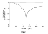
- FIG. 2 is a transmission characteristic diagram corresponding to an example of the acoustic wave resonator of FIG. 1
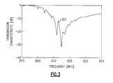
- FIG. 3 is a transmission characteristic diagram according to the conventional acoustic wave resonator of FIG. 19
- FIG. 4 is a diagram illustrating another configuration of an example of the acoustic wave resonator of FIG. 1
- FIG. 5 is a diagram illustrating another configuration of an example of the acoustic wave resonator of FIG. 1
- FIG. 6 is a diagram illustrating one example of comb-shaped electrodes for one embodiment of the acoustic wave resonator of FIG. 1;
- FIG. 1 is a diagram illustrating one example of an acoustic wave resonator according to one embodiment
- FIG. 2 is a transmission characteristic diagram corresponding to an example of the acoustic wave resonator of FIG. 1
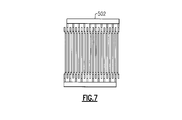
- FIG. 7 is a diagram illustrating another example of comb-shaped electrodes for another embodiment of the acoustic wave resonator of FIG. 1;
- FIG. 8 is a diagram illustrating one example of an acoustic wave resonator according to another embodiment;
- FIG. 9 is a transmission characteristic diagram corresponding to an example of the acoustic wave resonator of FIG. 8;
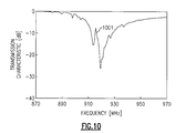
- FIG. 10 is a transmission characteristic diagram according to a conventional acoustic wave resonator;
- FIG. 11 is a cross-sectional view of the acoustic wave resonator of FIG. 8;
- FIG. 12 is a transmission characteristic diagram corresponding to one example of the acoustic wave resonator of FIG. 8;
- FIG. 13 is a transmission characteristic diagram according to a conventional acoustic wave resonator
- FIG. 14 is a diagram illustrating another configuration of an example of the acoustic wave resonator of FIG. 8
- FIG. 15 is a diagram of an acoustic wave filter including examples of the acoustic wave resonator according to FIG. 1 and/or FIG. 8
- FIG. 16 is a block diagram of one example of an antenna duplexer including the acoustic wave filter of FIG. 15, according to certain embodiments
- FIG. 17 is a block diagram of one example of a module incorporating the acoustic wave filter of FIG. 15, according to certain embodiments
- FIG. 18 is a block diagram of one example of a wireless communications device incorporating the antenna duplexer of FIG. 16, according to certain embodiments;
- FIG. 19 is a diagram illustrating one configuration of a conventional acoustic wave resonator; and
- FIG. 20 is a diagram illustrating another configuration of a conventional acoustic wave resonator.
- the acoustic wave resonator 100 includes comb-shaped electrodes 102 and reflector electrodes 103 that are formed on a piezoelectric substrate 101.
- the acoustic wave resonator 100 is configured with an overlapping portion between the comb-shaped electrodes 102 to excite an acoustic wave, the overlapping portion including a first overlapping region 104 and second overlapping regions 105.
- the second overlapping regions 105 are provided on both outside edges of the first overlapping region 104, as shown in FIG. 1.
- the electrode fingers of the first overlapping region 104 and the electrode fingers of the second overlapping regions 105 are connected via first connection electrode fingers 106.
- the first connection electrode fingers 106 are provided in first connection regions, each of which is located between the first overlapping region 104 and the second overlapping region 105.
- the electrode fingers of the second overlapping region 105 and the electrode fingers of a dummy region 107 are connected via second connection electrode fingers 108.
- the second connection electrode fingers 108 are provided in second connection regions, each of which is located between the second overlapping region 105 and the busbar electrode 110.
- the dummy region 107 refers to a region where the electrode fingers do not overlap with each other between the comb-shaped electrodes 102. In the example illustrated in FIG.
- the first connection electrode fingers 106 and the second connection electrode fingers 108 are connected in a direction oblique with respect to the direction in which the electrode fingers of the comb-shaped electrode 102 extend. Further, the direction in which the first connection electrode fingers 106 extend is opposite to the direction in which the second connection electrode fingers 108 extend. As a result, the electrode fingers of the first overlapping region 104 are arranged collinear with the electrode fingers of the dummy region 107.
- the first overlapping region 104 is a main portion for exciting an acoustic wave to obtain desired frequency characteristics.
- the overlapping width (W) of the first overlapping region 104 is greater than the overlapping width of the second overlapping region 105.
- the electrode finger pitch of the second overlapping region 105 may be greater than the electrode finger pitch of the first overlapping region 104, and as a result, the frequency of an acoustic wave excited in the second overlapping region 105 may be lower than the frequency of an acoustic wave excited in the first overlapping region 104.
- the electrode finger pitch refers to the distance between the centers of adjacent electrode fingers.
- FIG. 2 illustrates a transmission characteristic for the acoustic wave resonator of FIG. 1.
- FIG. 3 illustrates a transmission characteristic for the conventional acoustic wave resonator of FIG. 19.
- a 128-degree LiNbO 3 substrate is used for the piezoelectric substrate so that the main acoustic wave can be a Rayleigh wave.
- the electrode finger pitch of the first overlapping region 104 is 2.00 ⁇ m
- the electrode finger pitch of the second overlapping region 105 is 2.02 ⁇ m.
- the number of electrode fingers of the comb-shaped electrode 102 is one hundred (100), and the number of the electrode fingers of the reflector 103 is thirty (30).
- the metallization ratio of the electrode fingers of the second overlapping region 105 is the same as that of the electrode fingers of the first overlapping region 104.
- the metallization ratio is defined as the electrode finger width/(the electrode finger width + the space between the electrode fingers).
- the electrode finger pitch of the second overlapping region 105 is configured to be greater than that of the first overlapping region. Accordingly, the width of the electrode fingers in the second overlapping region 105 is greater than the width of the electrode fingers in the first overlapping region 104. As shown in FIG.
- examples of the acoustic wave resonator 100 according to embodiments of the present invention can suppress spuriousness.
- the suppression of spuriousness can be attributed to the configuration in which the frequency of an acoustic wave excited in the second overlapping region 105 is lower than the frequency of an acoustic wave excited in the first overlapping region 104, achieved by increasing the electrode finger pitch of the second overlapping region 105 in comparison with the electrode finger pitch of the first overlapping region 104.
- embodiments of the acoustic wave resonator according to aspects of the present invention can suppress spuriousness in the transmission characteristic of the acoustic wave resonator such that a downsized acoustic wave resonator having improved characteristics can be realized.
- Certain embodiments of the acoustic wave resonator 100 are configured to eliminate dummy electrode fingers (electrode fingers that do not extend to the second overlapping region 105) in the dummy region 107 of the comb-shaped electrode 102.
- dummy electrode fingers electrode fingers that do not extend to the second overlapping region 105
- other embodiments can use comb-shaped electrodes 402 provided with such dummy electrode fingers, as shown in FIG. 4, for example.
- the electrode finger pitch is greatest in the second overlapping region 105
- comb-shaped electrodes 502 and reflector electrodes 503 can be used in which the electrode finger pitch is greatest in the dummy region 501.
- An example of this configuration is illustrated in FIG. 5.
- the propagation direction length of the busbar electrode 510 connected to the electrode fingers of the comb-shaped electrode 502 is greater than the propagation direction length (L) of the first overlapping region 104 of the comb-shaped electrode 502.
- This configuration can eliminate the second connection electrode fingers 108, which may allow the overlapping width to be reduced.
- Similar effects can be achieved using other configurations of the comb-shaped electrodes 102, 502, such as those illustrated in FIGS. 6 and 7, for example. Still further, similar effects can be achieved in a longitudinal-mode-type surface acoustic wave filter in which a plurality of comb-shaped electrodes (i.e., including comb-shaped electrodes similar to any of the comb-shaped electrodes 102, 402, 502, etc.) are adjacently arranged in the propagation direction of an acoustic wave.
- a plurality of comb-shaped electrodes i.e., including comb-shaped electrodes similar to any of the comb-shaped electrodes 102, 402, 502, etc.
- a Y-cut 128-degree LiNbO 3 substrate is used for the piezoelectric substrate of the acoustic wave filter; however, embodiments of the acoustic wave resonator are not limited in this regard, and other piezoelectric substrates can be used.
- suppression of spuriousness in the transverse mode can be achieved by embodiments of the acoustic wave filter of FIG. 1 using a LiNbO 3 substrate wherein the cut angle ranges from 120 degrees to 135 degrees in Y-cut, such that an acoustic wave resonator having improved characteristics can be realized.
- the material of the electrodes is not limited to the specific examples disclosed herein, and a layered structure of high density electrodes with Aluminum-based materials, or a single layer electrode can be implemented.
- the number of the comb-shaped electrodes and reflector electrodes and the electrode finger pitch are not limited to the specific examples disclosed herein.
- certain embodiments include second overlapping regions 105 that are the same and provided on both sides in the overlapping width direction of the first overlapping region 104, in other examples, the second overlapping regions 105 differ from one another. Similar effects can be achieved at least by a configuration in which the frequency of an acoustic wave excited by the second overlapping regions 105 is lowered in comparison with that of an acoustic wave excited by the first overlapping region 104.
- the acoustic wave resonator 100 is configured such that the electrode finger pitch of the second overlapping region 105 is greater than the electrode finger pitch of the first overlapping region 104 throughout the whole region of the comb-shaped electrode in the propagation direction of an acoustic wave.
- the electrode finger pitch of the second overlapping region 105 can be the same as or less than the electrode finger pitch of the first overlapping region 104 around both edges of the comb-shaped electrode in the propagation direction of an acoustic wave (in portions adjacent to the reflectors 103).
- the effects discussed above can be achieved provided that the frequency of an acoustic wave excited by the second overlapping region 105 is lower than the frequency of an acoustic wave excited by the first overlapping region 104.
- a portion lacking the second overlapping region can be included in a portion of the comb-shaped electrode.
- the metallization ratios are the same between the first overlapping region 104 and the second overlapping region 105, in other examples the metallization ratios can be different. A similar effect can be obtained provided that the frequency of an acoustic wave in the second overlapping region 105 is lower than the frequency of an acoustic wave in the first overlapping region 104.
- a filter and an antenna duplexer to use embodiments of the acoustic wave resonator 100 according to this disclosure can realize a filter and/or an antenna duplexer having less spuriousness in the transverse mode and improved characteristics, as well as a module and a communication device having enhanced performance using the same, as discussed further below.
- the configuration of this example includes first phase region electrode fingers 809 and second phase region electrode fingers 811, the phase of an acoustic wave generated by the first phase region electrode fingers 809 being different from the phase of an acoustic wave generated by the second phase region electrode fingers 811.
- the electrode fingers of the first overlapping region 804 connected to the first phase region electrode fingers 809 have a 180-degree difference relationship with the electrode fingers of the first overlapping region 804 connected to the second phase region electrode fingers 811.
- the phase of an acoustic wave in the first phase region is different from the phase of an acoustic wave in the second phase region.
- the first and the second connection electrode fingers 806, 808 are connected in a direction opposite and oblique with each other to the first and the second phase region electrode fingers 809, 811.
- FIG. 9 shows a transmission characteristic for one example of the acoustic wave resonator 800 of FIG. 8.
- FIG. 10 shows a transmission characteristic according to the conventional acoustic wave resonator of FIG. 19.
- a 128-degree LiNbO 3 substrate is used for the piezoelectric substrate so that a Rayleigh wave is the main acoustic wave.
- the electrode finger pitch of the first overlapping region 804 is 2.00 ⁇ m
- the electrode finger pitch of the second overlapping region 805 is 2.02 ⁇ m.
- the number of the electrode fingers of the comb-shaped electrode is two hundred (200), and the number of the electrode fingers of the reflector is thirty (30). As shown in FIG.
- embodiments of the acoustic wave resonator 800 can suppress the spuriousness.
- the suppression of the spuriousness can be attributed to the configuration in which the frequency of an acoustic wave excited in the second overlapping region 805 is lower than the frequency of an acoustic wave excited in the first overlapping region 804, achieved, for example, by increasing the electrode finger pitch of the second overlapping region 805 in comparison with the electrode finger pitch of the first overlapping region 804.
- embodiments of the acoustic wave resonator 800 can suppress spuriousness in the transmission characteristic of the acoustic wave resonator so that an improved acoustic wave resonator can be realized. Furthermore, configuring the comb-shaped electrode 802 to have the number of the electric fingers in the second overlapping region 805 be less than that of the first overlapping region 804 can prevent defectively formed electrodes caused by the first and the second connection electrodes 807, 808 being too thin to perform sufficient exposure, etching and the like.
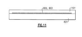
- the comb-shaped electrode 802 and the reflector electrodes 803 may be covered with a dielectric thin film 1101.
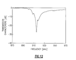
- FIG. 12 shows a transmission characteristic of an example of the acoustic wave resonator when a SiO 2 thin film is used for the dielectric thin film 1101. The thickness of the SiO 2 thin film can be approximately 33% of the normalized wavelength.
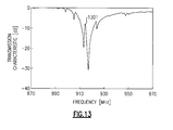
- FIG. 13 shows a transmission characteristic for an example in which the comb-shaped electrodes and the reflector electrodes of a conventional acoustic wave resonator are covered with a SiO 2 thin film. As shown in FIG.
- greater spuriousness 1301 occurs on the lower side of the anti-resonant frequency in the transmission characteristic of the conventional acoustic wave resonator.
- embodiments of the acoustic wave resonator 800 according to aspects of the present invention can suppress the spuriousness even when the coating of a SiO 2 thin film exists.
- the acoustic wave resonator 800 according to embodiments disclosed herein can improve the temperature characteristic of the acoustic wave resonator, and devices including such acoustic wave resonators with the SiO 2 thin film.
- Certain embodiments of the acoustic wave resonator 800 are configured to eliminate dummy electrode fingers in the dummy region 807 of the comb-shaped electrode 802.
- other embodiments can use comb-shaped electrodes 402 provided with such dummy electrode fingers, similar to the example as shown in FIG. 4.
- the electrode finger pitch is greatest in the second overlapping region 805; other examples can use comb-shaped electrodes 1402 and reflector electrodes 1403 in which the electrode finger pitch is greater in the dummy region 1401, as shown in FIG. 14, for example.
- the propagation direction length of the busbar electrode 1410 connected to the electrode fingers of the comb-shaped electrode 1402 is greater than the propagation direction length of the first overlapping region 804 of the comb-shaped electrode 1402. This configuration can eliminate the second connection electrode fingers 808 and therefore the overlapping width can be reduced.
- the effect of reduced spuriousness and other advantages can be achieved using a variety of configurations of the comb-shaped electrodes 102, 402, 502, 802, 1402. Still further, similar effects can be achieved in a longitudinal-mode-type surface acoustic wave filter in which a plurality of comb-shaped electrodes 102, 402, 502, 802, 1402 are adjacently arranged in the propagation direction of an acoustic wave.
- a Y-cut 128-degree LiNbO 3 substrate is used for the piezoelectric substrate of the acoustic wave filter; however, embodiments of the acoustic wave resonator are not limited in this regard, and other piezoelectric substrates can be used.
- suppression of spuriousness in the transverse mode can be achieved by embodiments of the acoustic wave filter of FIG. 8 using a LiNbO 3 substrate wherein the cut angle ranges from 120 degrees to 135 degrees in Y-cut, such that an acoustic wave resonator having an improved characteristic can be realized.
- the material of the electrodes is not limited to the specific examples disclosed herein, and a layered structure of high density electrodes with Aluminum-based materials, or a single layer electrode can be implemented.
- the number of the comb-shaped electrodes and reflector electrodes and the electrode finger pitch are not limited to the specific example of FIG. 8.
- the second overlapping regions 805 provided on both sides in the overlapping width direction of the first overlapping region 804 are the same in some examples, the second overlapping regions 805 can be different in other examples.
- the similar effect can be achieved at least by configurations in which the frequency of an acoustic wave excited by the second overlapping regions 805 is lower in comparison with that of an acoustic wave excited by the first overlapping region.
- the thickness of SiO 2 layer is not limited to this specific example and can be optimized according to the acoustic velocity of the main acoustic wave, other spuriousness, the cut angle, and the like. Still further, a similar effect can be achieved in embodiments of the acoustic wave filter of FIG. 1 when a coating of the SiO 2 thin film is included.
- a filter and an antenna duplexer to use embodiments of the acoustic wave resonator 800 according to this disclosure can realize a filter and/or an antenna duplexer having less spuriousness in the transverse mode and improved characteristics, as well as a module and/or a communication device having enhanced performance using the same.
- FIG. 15 illustrates an example of a ladder-type acoustic wave filter 1500 in which embodiments of the acoustic wave resonator 100 and/or 800 may be used.
- the acoustic wave filter 1500 includes one or more series arm resonators 1505a and one or more parallel arm resonators 1505b. In the example illustrated in FIG.
- the acoustic wave filter 1500 includes three series arm resonators 1505a and two parallel arm resonators 1505b; however, it is to be appreciated that embodiments of the acoustic wave filter are not so limited and may include any number of series arm and parallel arm resonators.
- the series arm resonators 1505a are connected in series along a signal path between a first terminal 1501 and a second terminal 1503.
- the parallel arm resonators 1505b are connected between the signal path and a ground 1507. Any one or more of the series arm resonators 1505a and/or parallel arm resonators 1505b can be an embodiment of the acoustic wave resonators 100 or 800 discussed above.
- Embodiments of the acoustic wave resonators 100 and 800 can suppress spuriousness in the transmission characteristic of the acoustic wave resonator, such that a downsized acoustic wave resonator having improved characteristics can be realized.
- Embodiments of the acoustic wave resonator 800 may also have an improved temperature characteristic. Accordingly, incorporation of one or more of these acoustic wave resonators 100, 800 into the acoustic wave filter 1500 can provide a filter having improved characteristics, such as smaller size, improved transmission characteristics (including reduced spuriousness), and improved temperature stability or performance, for example.
- the acoustic wave filter 1500 may be used to provide an antenna duplexer having improved characteristics.
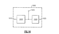
- FIG. 16 illustrates a block diagram of one example of an antenna duplexer which may incorporate embodiments of the acoustic wave filter 1500, and therefore embodiments of the acoustic wave resonators 100 and/or 800.
- the antenna duplexer 1600 includes a transmission filter 1610 and a reception filter 1620 that are connected to a shared antenna terminal 1630.
- the transmission filter 1610 includes a transmission-side terminal 1615 for connecting the transmission filter to transmitter circuitry
- the reception filter includes a receive-side terminal 1625 for connecting the reception filter to receiver circuitry.
- Either or both of the transmission filter 1610 and the reception filter 1620 can be an embodiment of the acoustic wave filter 1500.
- the first terminal 1501 of the acoustic wave filter 1500 may correspond to the transmission-side terminal 1615
- the second terminal 1503 of the acoustic wave resonator 1500 may correspond to the antenna terminal 1630.
- the first terminal 1501 of the acoustic wave filter 1500 may correspond to the antenna terminal 1630
- the second terminal 1503 of the acoustic wave resonator 1500 may correspond to the receive-side terminal 1625.
- the antenna duplexer 1600 By configuring the antenna duplexer 1600 to use the acoustic wave filter 1500, which includes one or more of the acoustic wave resonators 100 and/or 800, an antenna duplexer having improved characteristics and enhanced performance (resulting from the improved characteristics of the acoustic wave resonators 100, 800 discussed above) can be realized.
- FIG. 17 is a block diagram illustrating one example of a filter module 1700 including the acoustic wave filter 1500 of FIG. 15.
- the module 1700 further includes connectivity 1710 to provide signal interconnections, packaging 1720, such as for example, a package substrate, for packaging of the circuitry, and other circuitry die 1730, such as, for example amplifiers, pre-filters, modulators, demodulators, down converters, and the like, as would be known to one of skill in the art of semiconductor fabrication in view of the disclosure herein.
- packaging 1720 such as for example, a package substrate
- other circuitry die 1730 such as, for example amplifiers, pre-filters, modulators, demodulators, down converters, and the like, as would be known to one of skill in the art of semiconductor fabrication in view of the disclosure herein.
- the acoustic wave filter 1500 in module 1700 may be replaced with the antenna duplexer 1600, so as to provide an RF module, for example.
- FIG. 18 is a schematic block diagram of one example of a communication device 1800 (e.g., a wireless or mobile device) that can include the antenna duplexer 1600 incorporating one or more acoustic wave resonators 100, 800, as discussed above.
- the communication device 1800 can represent a multi-band and/or multi-mode device such as a multi-band/multi-mode mobile phone, for example.
- the communication device 1800 can include the antenna duplexer 1600, a transmission circuit 1810 connected to the antenna duplexer via the transmission-side terminal 1615, a reception circuit 1820 connected to the antenna duplexer 1600 via the receive-side terminal 1625, and an antenna 1830 connected to the antenna duplexer via the antenna terminal 1630.
- the transmission circuit 1810 and reception circuit 1820 may be part of a transceiver that can generate RF signals for transmission via the antenna 1830 and can receive incoming RF signals from the antenna 1830.
- the communication device 1800 can further include a controller 1840, a computer readable medium 1850, a processor 1860, and a battery 1870.
- various functionalities associated with the transmission and receiving of RF signals can be achieved by one or more components that are represented in FIG. 18 as the transmission circuit 1810 and the reception circuit 1820.
- a single component can be configured to provide both transmitting and receiving functionalities.
- transmitting and receiving functionalities can be provided by separate components.
- various antenna functionalities associated with the transmission and receiving of RF signals can be achieved by one or more components that are collectively represented in FIG. 18 as the antenna 1830.
- a single antenna can be configured to provide both transmitting and receiving functionalities.
- transmitting and receiving functionalities can be provided by separate antennas.
- different bands associated with the communication device 1800 can be provided with different antennas.
- the antenna duplexer 1600 can be configured to electrically connect the antenna 1830 to a selected transmit or receive path.
- the antenna duplexer 1600 can provide a number of switching functionalities associated with an operation of the communication device 1800.
- the antenna duplexer 1600 includes the transmission filter 1610 and reception filter 1620, which are configured to provide filtering of the RF signals.
- the transmission filter 1610 and reception filter 1620 can include embodiments of the acoustic wave filter 1500 including one or more acoustic wave resonators 100 and/or 800, and thereby provide enhanced performance through the benefits of reduced spuriousness and improved characteristics achieved using embodiments of the acoustic wave resonators 100 and/or 800.
- a controller 1840 can be provided for controlling various functionalities associated with operations of the antenna duplexer 1600 and/or other operating component(s).
- a processor 1860 can be configured to facilitate implementation of various processes for operation of the communication device 1800.
- the processes performed by the processor 1860 may be implemented by computer program instructions.
- These computer program instructions may be provided to a processor of a general purpose computer, special purpose computer, or other programmable data processing apparatus to produce a machine, such that the instructions, which execute via the processor of the computer or other programmable data processing apparatus, create a mechanism for operating the communication device 1800.
- these computer program instructions may also be stored in the computer-readable medium 1850.
- the battery 1870 can be any suitable battery for use in the communication device 1800, including, for example, a lithium-ion battery.
Landscapes
- Physics & Mathematics (AREA)
- Acoustics & Sound (AREA)
- Surface Acoustic Wave Elements And Circuit Networks Thereof (AREA)
Priority Applications (1)
| Application Number | Priority Date | Filing Date | Title |
|---|---|---|---|
| JP2016561393A JP6513104B2 (ja) | 2014-04-08 | 2015-04-07 | 弾性波共振器、これを用いた弾性波フィルタ、アンテナ共用器、モジュール及び通信機器 |
Applications Claiming Priority (2)
| Application Number | Priority Date | Filing Date | Title |
|---|---|---|---|
| JP2014-079111 | 2014-04-08 | ||
| JP2014079111 | 2014-04-08 |
Publications (1)
| Publication Number | Publication Date |
|---|---|
| WO2015155984A1 true WO2015155984A1 (en) | 2015-10-15 |
Family
ID=52991916
Family Applications (1)
| Application Number | Title | Priority Date | Filing Date |
|---|---|---|---|
| PCT/JP2015/001956 Ceased WO2015155984A1 (en) | 2014-04-08 | 2015-04-07 | Acoustic wave resonators, acoustic wave filters, antenna duplexers, modules and communication devices using the same |
Country Status (3)
| Country | Link |
|---|---|
| US (2) | US9647635B2 (enExample) |
| JP (2) | JP6513104B2 (enExample) |
| WO (1) | WO2015155984A1 (enExample) |
Families Citing this family (15)
| Publication number | Priority date | Publication date | Assignee | Title |
|---|---|---|---|---|
| JP6513104B2 (ja) * | 2014-04-08 | 2019-05-15 | スカイワークスフィルターソリューションズジャパン株式会社 | 弾性波共振器、これを用いた弾性波フィルタ、アンテナ共用器、モジュール及び通信機器 |
| JP6445152B2 (ja) * | 2016-01-29 | 2018-12-26 | 京セラ株式会社 | 弾性波共振子、弾性波フィルタ、分波器および通信装置 |
| US10615773B2 (en) * | 2017-09-11 | 2020-04-07 | Akoustis, Inc. | Wireless communication infrastructure system configured with a single crystal piezo resonator and filter structure |
| US10056879B2 (en) * | 2016-04-21 | 2018-08-21 | Murata Manufacturing Co., Ltd. | Elastic wave filter device |
| JP6465441B2 (ja) * | 2016-07-29 | 2019-02-06 | 太陽誘電株式会社 | マルチプレクサ |
| KR101953219B1 (ko) * | 2016-11-24 | 2019-02-28 | 가부시키가이샤 무라타 세이사쿠쇼 | 탄성파 장치, 고주파 프론트 엔드 회로 및 통신 장치 |
| JP2020005161A (ja) * | 2018-06-29 | 2020-01-09 | 株式会社村田製作所 | フィルタおよびマルチプレクサ |
| US11502668B2 (en) | 2018-11-16 | 2022-11-15 | Skyworks Solutions, Inc. | Multi-mode surface acoustic wave filter with stepped acoustic reflectors |
| WO2021039639A1 (ja) * | 2019-08-30 | 2021-03-04 | 株式会社村田製作所 | 弾性波装置 |
| US12506464B2 (en) | 2021-12-06 | 2025-12-23 | Skyworks Solutions, Inc. | Multi-band surface acoustic wave filters |
| US20230261636A1 (en) * | 2022-02-11 | 2023-08-17 | RF360 Europe GmbH | Optimization of surface acoustic wave (saw) resonators with resonance frequency at upper stopband edge for filter design |
| US12525494B2 (en) | 2022-03-30 | 2026-01-13 | Skyworks Solutions, Inc. | Composited carrier for microphone package |
| JP2024104398A (ja) * | 2023-01-24 | 2024-08-05 | 株式会社村田製作所 | マルチプレクサ |
| CN118694340A (zh) * | 2023-03-24 | 2024-09-24 | 华为技术有限公司 | 声学滤波器及其制备方法、电子设备 |
| CN120880374B (zh) * | 2025-09-26 | 2026-03-24 | 锐石创芯(重庆)科技股份有限公司 | 弹性波装置及射频前端模组 |
Citations (7)
| Publication number | Priority date | Publication date | Assignee | Title |
|---|---|---|---|---|
| DE2656154A1 (de) * | 1975-12-19 | 1977-07-07 | Hans Dr Kuzmany | Elektroakustischer wandler zum einschreiben und auslesen von information aus einer zweidimensionalen oder dreidimensionalen matrix |
| JPS60180316A (ja) * | 1984-02-28 | 1985-09-14 | Japan Radio Co Ltd | 弾性表面波フイルタ |
| US5831492A (en) * | 1995-09-15 | 1998-11-03 | Sawtek Inc. | Weighted tapered spudt saw device |
| US5973438A (en) * | 1998-02-13 | 1999-10-26 | Toda; Kohji | Ultrasonic switching device |
| EP1489741A1 (en) * | 2003-06-19 | 2004-12-22 | Seiko Epson Corporation | Surface acoustic wave filter and surface acoustic wave resonator |
| US20120286624A1 (en) * | 2010-03-04 | 2012-11-15 | Panasonic Corporation | Elastic wave device |
| US20130278358A1 (en) * | 2012-04-18 | 2013-10-24 | Nihon Dempa Kogyo Co., Ltd. | Elastic wave filter |
Family Cites Families (14)
| Publication number | Priority date | Publication date | Assignee | Title |
|---|---|---|---|---|
| JPS6043912A (ja) * | 1983-08-22 | 1985-03-08 | Toshiba Corp | 弾性表面波共振子 |
| US5289073A (en) * | 1992-11-09 | 1994-02-22 | The United States Of America As Represented By The Secretary Of The Army | Unidirectional surface acoustic wave transducer |
| JPH0750548A (ja) * | 1993-05-31 | 1995-02-21 | Canon Inc | 弾性表面波素子 |
| JPH09162679A (ja) * | 1995-12-01 | 1997-06-20 | Japan Energy Corp | 弾性表面波装置 |
| GB9622654D0 (en) * | 1996-10-31 | 1997-01-08 | Flowers James E | Filters |
| JP4821079B2 (ja) * | 2001-07-04 | 2011-11-24 | 株式会社村田製作所 | 弾性表面波用のくし型電極部、弾性表面波装置、通信装置 |
| TWI315607B (en) * | 2001-10-29 | 2009-10-01 | Panasonic Corp | Surface acoustic wave filter element, surface acoustic wave filter and communication device using the same |
| US6924715B2 (en) * | 2002-02-12 | 2005-08-02 | Nortel Networks Limited | Band reject filters |
| DE10314153A1 (de) * | 2003-03-28 | 2004-10-07 | Epcos Ag | Oberflächenwellen-Anordnung zur breitbandigen Signalübertragung |
| JP2006203680A (ja) * | 2005-01-21 | 2006-08-03 | Seiko Epson Corp | 弾性表面波フィルタ |
| JP2010010874A (ja) * | 2008-06-25 | 2010-01-14 | Epson Toyocom Corp | 弾性表面波フィルタ |
| JP5389459B2 (ja) * | 2009-01-30 | 2014-01-15 | 三洋電機株式会社 | 報知方法および無線装置 |
| JP5672050B2 (ja) * | 2011-02-21 | 2015-02-18 | 株式会社村田製作所 | 弾性表面波フィルタ装置 |
| JP6513104B2 (ja) * | 2014-04-08 | 2019-05-15 | スカイワークスフィルターソリューションズジャパン株式会社 | 弾性波共振器、これを用いた弾性波フィルタ、アンテナ共用器、モジュール及び通信機器 |
-
2015
- 2015-04-07 JP JP2016561393A patent/JP6513104B2/ja active Active
- 2015-04-07 WO PCT/JP2015/001956 patent/WO2015155984A1/en not_active Ceased
- 2015-04-07 US US14/680,486 patent/US9647635B2/en active Active
-
2017
- 2017-05-05 US US15/587,986 patent/US10305445B2/en active Active
-
2019
- 2019-04-09 JP JP2019074179A patent/JP6618646B2/ja active Active
Patent Citations (7)
| Publication number | Priority date | Publication date | Assignee | Title |
|---|---|---|---|---|
| DE2656154A1 (de) * | 1975-12-19 | 1977-07-07 | Hans Dr Kuzmany | Elektroakustischer wandler zum einschreiben und auslesen von information aus einer zweidimensionalen oder dreidimensionalen matrix |
| JPS60180316A (ja) * | 1984-02-28 | 1985-09-14 | Japan Radio Co Ltd | 弾性表面波フイルタ |
| US5831492A (en) * | 1995-09-15 | 1998-11-03 | Sawtek Inc. | Weighted tapered spudt saw device |
| US5973438A (en) * | 1998-02-13 | 1999-10-26 | Toda; Kohji | Ultrasonic switching device |
| EP1489741A1 (en) * | 2003-06-19 | 2004-12-22 | Seiko Epson Corporation | Surface acoustic wave filter and surface acoustic wave resonator |
| US20120286624A1 (en) * | 2010-03-04 | 2012-11-15 | Panasonic Corporation | Elastic wave device |
| US20130278358A1 (en) * | 2012-04-18 | 2013-10-24 | Nihon Dempa Kogyo Co., Ltd. | Elastic wave filter |
Also Published As
| Publication number | Publication date |
|---|---|
| JP2017511074A (ja) | 2017-04-13 |
| US20150288346A1 (en) | 2015-10-08 |
| JP6618646B2 (ja) | 2019-12-11 |
| JP2019146233A (ja) | 2019-08-29 |
| US20170244384A1 (en) | 2017-08-24 |
| US10305445B2 (en) | 2019-05-28 |
| US9647635B2 (en) | 2017-05-09 |
| JP6513104B2 (ja) | 2019-05-15 |
Similar Documents
| Publication | Publication Date | Title |
|---|---|---|
| US10305445B2 (en) | Elastic wave resonators and filters | |
| US9641151B2 (en) | Elastic wave filters and duplexers using same | |
| US10601570B2 (en) | Multiplexer, radio-frequency front-end circuit, and communication apparatus | |
| WO2016017104A1 (en) | Acoustic wave filters and duplexers using same | |
| JP6017868B2 (ja) | 分波器、フィルタ及び通信モジュール | |
| JP6822299B2 (ja) | 高周波フロントエンド回路および通信装置 | |
| US9236850B2 (en) | Signal separation device | |
| KR102526570B1 (ko) | 음향파 소자들, 안테나 듀플렉서들 및 전자 디바이스들 | |
| US10958241B2 (en) | Extractor | |
| JP2012156741A (ja) | アンテナ共用器 | |
| US20150002241A1 (en) | Duplexer | |
| KR20140079433A (ko) | 탄성파 분파기 | |
| JP6777161B2 (ja) | フィルタ装置およびマルチプレクサ | |
| CN110582939B (zh) | 多工器、高频前端电路以及通信装置 | |
| CN111164891A (zh) | 多工器、高频前端电路以及通信装置 | |
| EP2432123A1 (en) | Duplexer | |
| CN113940003A (zh) | 复合滤波器装置 | |
| HK1227184A1 (en) | Acoustic wave elements, antenna duplexers and electronic devices | |
| HK1235557A1 (en) | Acoustic wave filters and duplexers using same |
Legal Events
| Date | Code | Title | Description |
|---|---|---|---|
| 121 | Ep: the epo has been informed by wipo that ep was designated in this application |
Ref document number: 15717666 Country of ref document: EP Kind code of ref document: A1 |
|
| ENP | Entry into the national phase |
Ref document number: 2016561393 Country of ref document: JP Kind code of ref document: A |
|
| NENP | Non-entry into the national phase |
Ref country code: DE |
|
| 122 | Ep: pct application non-entry in european phase |
Ref document number: 15717666 Country of ref document: EP Kind code of ref document: A1 |