WO2015151385A1 - 放電管及びその製造方法 - Google Patents
放電管及びその製造方法 Download PDFInfo
- Publication number
- WO2015151385A1 WO2015151385A1 PCT/JP2015/000648 JP2015000648W WO2015151385A1 WO 2015151385 A1 WO2015151385 A1 WO 2015151385A1 JP 2015000648 W JP2015000648 W JP 2015000648W WO 2015151385 A1 WO2015151385 A1 WO 2015151385A1
- Authority
- WO
- WIPO (PCT)
- Prior art keywords
- discharge
- active layer
- discharge tube
- atomic
- sealing
- Prior art date
- Legal status (The legal status is an assumption and is not a legal conclusion. Google has not performed a legal analysis and makes no representation as to the accuracy of the status listed.)
- Ceased
Links
Images



Classifications
-
- H—ELECTRICITY
- H01—ELECTRIC ELEMENTS
- H01T—SPARK GAPS; OVERVOLTAGE ARRESTERS USING SPARK GAPS; SPARKING PLUGS; CORONA DEVICES; GENERATING IONS TO BE INTRODUCED INTO NON-ENCLOSED GASES
- H01T1/00—Details of spark gaps
- H01T1/20—Means for starting arc or facilitating ignition of spark gap
- H01T1/22—Means for starting arc or facilitating ignition of spark gap by the shape or the composition of the electrodes
-
- H—ELECTRICITY
- H01—ELECTRIC ELEMENTS
- H01T—SPARK GAPS; OVERVOLTAGE ARRESTERS USING SPARK GAPS; SPARKING PLUGS; CORONA DEVICES; GENERATING IONS TO BE INTRODUCED INTO NON-ENCLOSED GASES
- H01T21/00—Apparatus or processes specially adapted for the manufacture or maintenance of spark gaps or sparking plugs
-
- H—ELECTRICITY
- H01—ELECTRIC ELEMENTS
- H01T—SPARK GAPS; OVERVOLTAGE ARRESTERS USING SPARK GAPS; SPARKING PLUGS; CORONA DEVICES; GENERATING IONS TO BE INTRODUCED INTO NON-ENCLOSED GASES
- H01T4/00—Overvoltage arresters using spark gaps
- H01T4/10—Overvoltage arresters using spark gaps having a single gap or a plurality of gaps in parallel
- H01T4/12—Overvoltage arresters using spark gaps having a single gap or a plurality of gaps in parallel hermetically sealed
Definitions
- the present invention relates to a surge absorber for protecting various devices from, for example, a surge generated by a lightning strike and the like, a discharge tube used as a switching spark gap for lighting an ignition plug, and a manufacturing method thereof.
- Discharge tubes are also used as switching spark gaps for gas arresters, high-pressure discharge lamps and ignition plugs, which are surge absorbers used to prevent electronic devices from failing due to the invasion of overvoltages such as lightning surges and static electricity. .
- Patent Document 1 proposes a surge absorbing element in which a plurality of discharge electrodes are arranged with a discharge gap therebetween and are enclosed in a hermetic envelope together with a discharge gas.
- the surface of the discharge electrode is formed with a film containing titanium carbide and an alkali metal such as Cs 2 CO 3 and / or an alkaline earth metal carbonate such as BaCO 3.
- This discharge activation material is obtained by adding an alkali metal carbonate powder and / or an alkaline earth metal carbon salt powder and a titanium carbide powder to a binder composed of sodium silicate and pure water. It is formed by applying to the surface of the discharge electrode.
- Patent Document 2 in order to obtain stability of discharge voltage after a surge current load, that is, repetitive operation stability, as a discharge activation material, sodium silicate (Na 2 SiO 3 ), cesium silicate as a base component (Cs 2 SiO 3 ), potassium silicate (K 2 SiO 3 ), cesium tungstate (Cs 2 WO 4 ) and titanium metal (Ti), and sodium tetraborate (Na 2 B 4 O as additives) 7 ) and a discharge tube in which a discharge active layer containing magnesium oxide (MgO) is formed has been proposed.
- sodium silicate Na 2 SiO 3
- cesium silicate as a base component
- K 2 SiO 3 cesium tungstate
- Ti cesium tungstate
- Na 2 B 4 O sodium tetraborate
- the present invention has been made in view of the above-described problems, and an object of the present invention is to provide a discharge tube capable of improving the stability of an operating voltage against repeated discharge and a method for manufacturing the same.
- the discharge tube according to the first invention includes at least one insulating hollow body having a plurality of openings, and at least two sealing electrodes that close the openings and seal the discharge control gas therein.
- a discharge active layer is formed on the surface of the sealing electrode exposed in the insulating hollow body, the discharge active layer contains Na, Si, Cs, C and O, and the remainder is unavoidable It is made of an impurity, is amorphous, and is characterized in that Na, Si, Cs, C, and O are uniformly distributed.
- a discharge tube according to a second invention is characterized in that, in the first invention, the Cs concentration in the discharge active layer is in the range of 1 atomic% ⁇ Cs ⁇ 7 atomic%. That is, in this discharge tube, since the Cs concentration in the discharge active layer is in the range of 1 atomic% ⁇ Cs ⁇ 7 atomic%, a sufficient discharge stabilizing effect can be obtained.
- the manufacturing method of the discharge tube which concerns on 3rd invention is a method of manufacturing the discharge tube which is 1st or 2nd invention, Comprising: A cesium carbonate powder is added to a sodium silicate solution, and a precursor is formed. Heat treatment at a temperature equal to or higher than a temperature at which sodium silicate softens and a temperature at which cesium carbonate melts and decomposes with respect to the applied precursor. And the step of performing.
- Patent Document 1 a discharge activation material containing an alkaline earth metal such as barium carbonate or an alkali metal carbonate such as cesium carbonate is described, but silicic acid to which a carbonate which is a crystalline substance is added. Since only the sodium solution is applied to the electrode surface, the applied discharge activation material contains crystalline carbonate. Moreover, sodium silicate also, for example, for capable of forming a crystal structure, such as Na 2 SiO 3, the discharge activation material applied is considered to form a coating film containing a large amount of crystalline material.
- the discharge active layer is amorphous and Na, Si, Cs, C and O are uniformly distributed, a cation containing Cs having excellent electron emission characteristics. High stability of the operating voltage against repeated discharge can be obtained by the discharge active layer of the amorphous glass material in which the elements are uniformly distributed.
- a precursor obtained by adding cesium carbonate powder to a sodium silicate solution is subjected to heat treatment at a temperature not lower than the temperature at which sodium silicate softens and not lower than the temperature at which cesium carbonate melts and decomposes. Since the component generated by the decomposition of cesium carbonate by heat treatment is uniformly diffused in the softened amorphous glass sodium silicate, each of Na, Si, Cs, C and O Elements can be uniformly distributed in the discharge active layer.
- an amorphous discharge active layer in which each element is uniformly distributed in the layer is formed by a heat treatment process that takes into consideration the melting point and decomposition temperature of each substance as a raw material.
- Cs having a large influence on the electron emission characteristics is uniformly distributed in a decomposed state, not in a crystalline cesium carbonate state, so that stable discharge characteristics can be obtained over the entire discharge surface. That is, arc discharge at the time of discharge is locally generated between the opposing discharge electrodes, and since the generation location thereof is stochastically random, compared to the conventional technique in which Cs locally exists in a crystalline state,
- the present invention having a discharge active layer having a uniform Cs distribution can provide stability with high discharge characteristics.
- cesium tungstate which is a Cs-based additive used in Patent Document 2
- Cs cesium tungstate having high thermal stability is used as the Cs source as compared with the case where cesium carbonate is used as the Cs source
- Cs is contained in sodium silicate only by adding cesium tungstate. It is difficult to realize a uniformly distributed amorphous structure.
- cesium tungstate is added with sodium silicate. The product is produced as a complex that is phase-separated macroscopically.
- cesium carbonate having a melting point lower than that of cesium tungstate as a Cs source
- cesium carbonate is dissolved and decomposed by heat treatment, and Cs is distributed in sodium silicate without causing phase separation.
- the component generated by the decomposition of cesium carbonate by heat treatment is in an amorphous state in the softened and fluidized amorphous glass network structure of sodium silicate, and Cs is uniformly distributed in the discharge activity.
- a layer can be formed.
- a discharge tube manufacturing method wherein the Cs concentration of the precursor is such that the Cs concentration in the discharge active layer finally formed on the electrode surface is 1 atomic% ⁇ Cs ⁇ . It is contained so that it may become in the range of 7 atomic%. That is, in this discharge tube manufacturing method, the Cs concentration of the precursor is contained so that the Cs concentration in the discharge active layer finally formed on the electrode surface is in the range of 1 atomic% ⁇ Cs ⁇ 7 atomic%. Therefore, a sufficient discharge stabilizing effect of Cs addition and a good distribution state of Cs can be obtained. When Cs is less than 1 atomic%, the amount of Cs added is small, and a sufficient discharge stabilization effect cannot be obtained. When Cs exceeds 7 atomic%, phase separation or crystallization tends to occur in part.
- the present invention has the following effects. That is, according to the discharge tube of the present invention, since the discharge active layer is amorphous and Na, Si, Cs, C, and O are uniformly distributed, the operation voltage is stable against repeated discharge. Sex is obtained. Further, according to the method for manufacturing a discharge tube of the present invention, by using cesium carbonate having a melting point lower than that of cesium tungstate as the Cs source, cesium carbonate is dissolved and decomposed by heat treatment, and phase separation does not occur. Cs can be uniformly distributed in sodium acid.
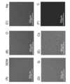
- FIG. 1 shows an SEM image (A) showing an example of a discharge tube and a method for producing the same according to the present invention, and SEM-EDX (energy dispersive X-ray) analysis images (B to F) of each element.
- SEM-EDX energy dispersive X-ray analysis images
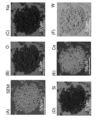
- FIG. 2 is an SEM image (A) showing comparative examples according to the present invention and SEM-EDX analysis images (B to F) of each element.
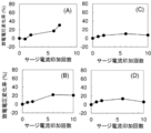
- FIG. 6 is a graph showing a discharge voltage change rate with respect to the number of surge currents applied in Comparative Example (A) and Examples (B to D) according to the present invention. It is a graph which shows the discharge voltage change rate with respect to the frequency
- the discharge tube 1 of this embodiment includes one insulating hollow body 2 having a plurality of openings, and two seals that close the openings and seal the discharge control gas inside. And an electrode 3.
- a discharge active layer 4 is formed on the opposing surfaces of the pair of sealing electrodes 3 exposed in the insulating hollow body 2.
- This discharge active layer 4 contains Na, Si, Cs, C and O, the remainder is made of inevitable impurities, is amorphous, and Na, Si, Cs, C and O are uniformly distributed. .
- the Cs concentration in the discharge active layer 4 is preferably in the range of 1 atomic% ⁇ Cs ⁇ 7 atomic%.
- whether or not each of the above elements is uniformly distributed in the discharge active layer 4 is determined based on the absence of phase separation of 1 ⁇ m or more when the SEM-EDX analysis is performed. Whether the discharge active layer 4 is amorphous or not is determined by X-ray diffraction analysis at room temperature, except those derived from members other than the discharge active layer 4, and the diffraction peak of the crystal phase of the constituent material of the discharge active layer 4. Judgment is made based on clear indications.
- the insulating hollow body 2 is a ceramic cylinder and is an insulating tube made of, for example, cylindrical alumina.
- the insulating hollow body 2 is preferably a crystalline ceramic material such as alumina.
- the pair of sealing electrodes 3 is a convex metal member such as copper, copper alloy, or 42Ni alloy having a convex portion 3a protruding inward, and a discharge gap is formed between the convex portions 3a facing each other. Yes. Note that lattice-shaped protrusions are formed on the end surface of the protrusion 3a, and the discharge active layer 4 is provided so as to fill a plurality of recesses 3b formed between the protrusions. . Further, these sealing electrodes 3 are joined and sealed to the insulating hollow body 2 by a sealing material 6 such as a brazing material.
- the discharge control gas is He, Ne, Ar, Kr, Xe, SF 6 , N 2 , CO 2 , C 3 F 8 , C 2 F 6 , CF 4 , H 2 or a mixed gas thereof.
- the manufacturing method of the discharge tube 1 of the present embodiment includes a step of adding a cesium carbonate powder to a sodium silicate solution to form a precursor, a step of applying the precursor to the surface of the sealing electrode 3, and a coated precursor. Heat treatment at a temperature higher than the temperature at which sodium silicate softens and the temperature at which cesium carbonate melts and decomposes. Further, this manufacturing method includes a step of brazing the sealing electrode 3 to the opening of the insulating hollow body 2, and the brazing temperature in the brazing step as the heat treatment is equal to or higher than a temperature at which sodium silicate is softened. The temperature is higher than the melting point of cesium carbonate. The Cs concentration of the precursor is contained so that the Cs concentration in the discharge active layer 4 finally formed on the electrode surface is in the range of 1 atomic% ⁇ Cs ⁇ 7 atomic%.
- a precursor is prepared by adding cesium carbonate powder at a predetermined ratio to a sodium silicate solution so as to have a predetermined composition. That is, a viscous precursor for forming a discharge active layer is prepared by mixing a sodium silicate glass solution and cesium carbonate powder. At this time, the Cs concentration contained in the precursor is adjusted so that the Cs concentration in the discharge active layer 4 finally formed on the electrode surface is in the range of 1 atomic% ⁇ Cs ⁇ 7 atomic%.
- the surface of the sealing electrode 3 is coated with the prepared precursor.
- various liquid substances such as a stamp method, a printing method using a metal mask and a squeegee, a dipping method, a paste printing method, an ink jet method, a dispenser method, a spin coating method, and the like are desired. A method of coating in place can be used.
- the sealing electrode 3 whose tip portion surface is covered with the precursor and the insulating hollow body 2 are brazed in a discharge control gas atmosphere. Thereby, it becomes the structure where the discharge control gas was sealed inside the insulating hollow body 2.
- the brazing temperature is, for example, 820 ° C.
- the brazing material and cesium carbonate are melted and further heated to a temperature above the temperature at which the sodium silicate glass, which is an amorphous substance, is sufficiently softened and fluidized (heat treatment). Cesium diffusion into the amorphous glass network of sodium silicate occurs.
- the cation element containing cesium having excellent electron emission characteristics is uniformly distributed in the amorphous glass material, and the discharge active layer 4 is formed on the surface of the sealing electrode 3.
- the discharge active layer 4 is amorphous and Na, Si, Cs, C, and O are uniformly distributed, Cs having excellent electron emission characteristics can be obtained. High stability of the operating voltage against repeated discharge can be obtained by the discharge active layer 4 made of an amorphous glass material in which the cation element is uniformly distributed. In particular, when the Cs concentration in the discharge active layer 4 is in the range of 1 atomic% ⁇ Cs ⁇ 7 atomic%, a sufficient discharge stabilizing effect can be obtained.
- the temperature is equal to or higher than the temperature at which sodium silicate softens and the temperature at which cesium carbonate melts and decomposes with respect to a precursor obtained by adding cesium carbonate powder to a sodium silicate solution. Since the component generated by the decomposition of cesium carbonate by heat treatment is uniformly diffused in the softened amorphous glass sodium silicate, Na, Si, Cs, C And O can be uniformly distributed in the discharge active layer 4. Further, the Cs concentration of the precursor is contained so that the Cs concentration in the discharge active layer 4 finally formed on the electrode surface is in the range of 1 atomic% ⁇ Cs ⁇ 7 atomic%. A sufficient discharge stabilization effect and a good distribution state of Cs can be obtained.
- Table 1 shows the result of analyzing the constituent element composition of the discharge active layer formed using a plurality of precursors by changing the ratio of sodium silicate and cesium carbonate.
- composition 1 is a comparative example in which cesium carbonate is not added and Cs is not contained, and compositions 2 and 3 contain Cs, but the Cs concentration is less than 1 atomic%.
- compositions 4 to 8 are examples of the present invention having a Cs concentration range suitable for the present invention (1 atomic% ⁇ Cs ⁇ 7 atomic%).
- the atomic concentration composition of the discharge active layer analyzed using 15 kV) is shown.
- Each atomic concentration and average concentration such as Cs concentration described in the present specification are atomic concentrations obtained by using the energy dispersive X-ray analysis method (acceleration voltage 15 kV).
- Composition 1 in Table 1 is an active layer produced using only a sodium silicate solution, but even if cesium carbonate is not used in this way, the carbon component mixed as an evaporated carbon or impurities is 9 at% ( Atomic%) is present.
- the amount of cesium carbonate added to sodium silicate is increased, a relatively high amount of carbon is detected, and as shown in composition 2 to composition 8, the presence of up to about 16 at% carbon is confirmed. This result shows that the carbon component derived from cesium carbonate remains in the discharge active layer. Note that some of the carbon components are vaporized by the heat treatment.
- an electrode-derived component of about 0.5 at% can be detected as an inevitable impurity in the discharge active layer due to a reaction between the discharge active layer material and the electrode component by heat treatment in the enclosing process.
- about 0.5 at% of Cu as an electrode component was detected from the discharge active layer of the present invention.
- the maximum heat treatment conditions are the same, almost the same amount of electrode-derived impurities (Cu) is detected in a wide Cs composition range, while the electrical characteristics of these discharge active layer materials depend on the amount of Cs. Even if an electrode-derived impurity is present in the active layer at about 0.5 at%, it is considered that the electrical characteristics of the active layer are hardly affected.
- FIG. 3 ((A) in the figure).
- This discharge active layer contains about 3 at% of Cs as an average concentration.
- no diffraction peak is detected other than the peak derived from the ceramic porcelain of the sealing electrode or insulating hollow body material. Therefore, this discharge active layer material is detected by X-ray diffraction analysis at room temperature. No possible crystal phase has been observed.
- cesium carbonate is a crystalline substance, and when cesium carbonate is heated to its melting point or higher, liquefaction due to melting and vaporization of the carbonic acid component due to thermal decomposition may occur. This process depends on heat treatment conditions, that is, temperature and time, and a part of the carbon component remains in the discharge active layer according to the conditions. Actually, as shown in the above-described embodiment, a maximum carbon component of about 16 at% is detected from the discharge active layer material heat-treated at a maximum of 820 ° C.
- the carbon component which exists in a discharge active layer has shown the uniform element distribution state like other elements, such as sodium, silicon, and cesium, so that the said analysis may show.
- This fact and the fact that the crystalline phase detectable by the X-ray diffraction analysis described above is not observed in the discharge active layer material cooled to room temperature are the same even when the carbon component remains in the active layer material.
- the component does not exist as a crystalline substance called cesium carbonate, but indicates that it exists in an amorphous glass network structure of sodium silicate in an amorphous state. That is, the discharge active layer material of the present invention has a structure that is essentially different from a composite material containing a crystalline substance called an alkali metal carbonate like conventional materials, while containing carbon.
- the temperature for realizing the amorphous glass having the uniform element distribution described above is a temperature of about 750 ° C. or higher at which the sodium silicate used in the present invention flows, and the melting point of cesium carbonate (commercially available reagent powder) It is preferable to be heated to a temperature of about 750 ° C., which is a melting point observed by thermal analysis, or 610 ° C. or more reported in other literatures, for example, 800 ° C. or more. From this, the heat treatment temperature of the example in the present invention is set to 820 ° C.
- FIG. 4 shows the results (SEM-EDX analysis results) of the images (BF). As can be seen from these images, the phase is largely separated into a phase mainly containing Na and Si and a phase mainly containing Cs and W.
- discharge characteristics of the gas arrester in which the discharge active layer is formed on the sealing electrode surface
- an insulating hollow body and a sealing electrode having the same dimensions were used, and the discharge control gas, pressure, and gas sealing process filled in the gas arrester were also constant.
- the discharge start voltage of each sample was made constant at 3500 V, and factors other than the composition of the discharge active layer material were made constant.
- This electrical characteristic evaluation is an evaluation of surge withstand characteristics, and is performed to compare the performance which is important when used as a lightning surge countermeasure part.
- the surge of 8A / 20 ⁇ s lightning surge waveform has a peak value of 4000 A. After the current was repeatedly applied to each sample, it was examined whether or not the initial discharge start voltage characteristics of each sample were maintained.
- surge withstand characteristics were similarly evaluated for a gas arrester in which a discharge active layer was formed using sodium silicate alone.
- the evaluation result of the comparative example is shown in FIG. 5A, and the evaluation result of the example of the present invention is that containing Cs of 2.0 at% (Example 1) and containing 3.9 at%.
- Examples (Example 2) and those containing 5.8 at% (Example 3) are shown in FIGS. 5B, 5C, and 5D in the order of description.
- the comparative example by repeatedly applying a surge current of 4000 A, the DC discharge start voltage greatly increased from the initial value, and no discharge response was observed when the eighth surge current was applied.
- Examples 1 to 3 of the present invention even after a surge current is repeatedly applied, a relatively stable discharge characteristic is exhibited and high durability is exhibited.
- FIGS. show the discharge characteristics of a gas arrester in which a discharge active layer is formed using a precursor prepared from a sodium silicate solution and a cesium tungstate powder.
- 6A shows a gas arrester in which a discharge active layer having a Cs average concentration of 2.8 at% is formed
- FIG. 6B shows a gas arrester in which a discharge active layer having a Cs average concentration of 3.8 at% is formed.
- the surge withstand characteristics are shown.
- the DC discharge start voltage is greatly increased from the initial value by repeatedly applying a surge current of 4000 A despite the addition of the Cs-based material.
- the present invention is applied to a discharge tube in which two openings of an insulating hollow body are closed by a pair of sealing electrodes, but the present invention is applied to a discharge tube having three or more electrodes. It doesn't matter.
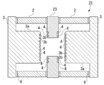
- the present invention may be applied to a discharge tube 21 in which a ring-shaped electrode 23 is provided at an intermediate portion between a pair of sealing electrodes 3. .
- a ring-shaped electrode 23 is fixed as a sealing electrode so as to close an opening between two insulating hollow bodies 2 arranged coaxially.
- the discharge active layer 4 is also formed on the ring electrode 23. That is, in the ring-shaped electrode 23, a plurality of concave portions 3b are formed on the surface of the sealing electrode 3 facing the convex portions 3a, and the discharge active layer 4 is provided so as to fill the concave portions 3b.
Landscapes
- Engineering & Computer Science (AREA)
- Manufacturing & Machinery (AREA)
- Glass Compositions (AREA)
- Gas-Filled Discharge Tubes (AREA)
Abstract
繰り返し放電に対する動作電圧の安定性を向上させることができる放電管及びその製造方法を提供する。 本発明の放電管は、複数の開口部を有する少なくとも一つの絶縁性中空体(2)と、開口部を閉塞して内部に放電制御ガスを封止する少なくとも2つの封止電極(3)とを備え、絶縁性中空体内に露出した封止電極の表面に、放電活性層(4)が形成されており、放電活性層が、Na,Si,Cs,C及びOを含有し、残部が不可避不純物からなり、非晶質であって、Na,Si,Cs,C及びOが均一に分布している。
Description
本発明は、例えば落雷等で発生するサージから様々な機器を保護し、事故を未然に防ぐためのサージアブソーバや、着火プラグ点灯用のスイッチングスパークギャップとして使用する放電管及びその製造方法に関する。
放電管は、例えば雷サージや静電気などの過電圧の侵入により電子機器などが故障することを防ぐために用いるサージアブソーバであるガスアレスタ、高圧放電ランプや着火プラグ用のスイッチングスパークギャップとしても採用されている。
このような雷サージ対策部品やスイッチングスパークギャップとしての放電管においては、繰り返し放電に対する動作電圧の安定性や優れた耐電圧特性などが要求される。このような繰返し動作安定性や優れた耐電圧特性等を得るために、放電電極の表面に放電活性化材料の被膜を形成する技術が検討されている。
従来、例えば特許文献1には、複数の放電電極を放電間隙を隔てて配置すると共に、これを放電ガスと共に気密外囲器内に封入したサージ吸収素子が提案されている。
従来、例えば特許文献1には、複数の放電電極を放電間隙を隔てて配置すると共に、これを放電ガスと共に気密外囲器内に封入したサージ吸収素子が提案されている。
このサージ吸収素子では、放電電極の表面に、Cs2CO3等のアルカリ金属及び/又はBaCO3等のアルカリ土類金属の炭酸塩と、炭化チタンが含有された被膜を形成することで、耐電圧特性の向上を図っている。この放電活性化材料は、アルカリ金属の炭酸塩の粉末及び/又はアルカリ土類金属の炭素塩の粉末と、炭化チタンの粉末とを、ケイ酸ナトリウムと純水よりなるバインダーに添加し、これを放電電極の表面に塗布することによって形成されている。
また、特許文献2では、サージ電流負荷後の放電電圧の安定性、すなわち繰り返し動作安定性を得るために、放電活性化材料として、ベース成分としてケイ酸ナトリウム(Na2SiO3)、ケイ酸セシウム(Cs2SiO3)、ケイ酸カリウム(K2SiO3)、タングステン酸セシウム(Cs2WO4)および金属チタン(Ti)を含有し、かつ添加剤として四ホウ酸ナトリウム(Na2B4O7)および酸化マグネシウム(MgO)を含有している放電活性層を形成した放電管が提案されている。
上記従来の技術には、以下の課題が残されている。
すなわち、上記従来技術では、アルカリ土類金属やアルカリ金属の炭酸塩を内包する放電活性化材料や、ケイ酸ナトリウムにケイ酸セシウム、ケイ酸カリウム、タングステン酸セシウム、金属チタン、四ホウ酸ナトリウム、酸化マグネシウムを含有した放電活性化材料を用いているが、それでも繰り返し放電に対して十分な動作電圧の安定性が得られていなかった。
すなわち、上記従来技術では、アルカリ土類金属やアルカリ金属の炭酸塩を内包する放電活性化材料や、ケイ酸ナトリウムにケイ酸セシウム、ケイ酸カリウム、タングステン酸セシウム、金属チタン、四ホウ酸ナトリウム、酸化マグネシウムを含有した放電活性化材料を用いているが、それでも繰り返し放電に対して十分な動作電圧の安定性が得られていなかった。
本発明は、前述の課題に鑑みてなされたもので、繰り返し放電に対する動作電圧の安定性を向上させることができる放電管及びその製造方法を提供することを目的とする。
本発明は、前記課題を解決するために以下の構成を採用した。すなわち、第1の発明に係る放電管は、複数の開口部を有する少なくとも一つの絶縁性中空体と、前記開口部を閉塞して内部に放電制御ガスを封止する少なくとも2つの封止電極とを備え、前記絶縁性中空体内に露出した前記封止電極の表面に、放電活性層が形成されており、前記放電活性層が、Na,Si,Cs,C及びOを含有し、残部が不可避不純物からなり、非晶質であって、Na,Si,Cs,C及びOが均一に分布していることを特徴とする。
第2の発明に係る放電管は、第1の発明において、前記放電活性層中におけるCs濃度が1原子%≦Cs≦7原子%の範囲内であることを特徴とする。
すなわち、この放電管では、放電活性層中におけるCs濃度が1原子%≦Cs≦7原子%の範囲内であるので、十分な放電安定効果を得ることができる。
すなわち、この放電管では、放電活性層中におけるCs濃度が1原子%≦Cs≦7原子%の範囲内であるので、十分な放電安定効果を得ることができる。
また、第3の発明に係る放電管の製造方法は、第1又は第2の発明である放電管を製造する方法であって、ケイ酸ナトリウム溶液に炭酸セシウム粉末を加えて前駆体を形成する工程と、前記前駆体を前記封止電極の表面に塗布する工程と、塗布された前記前駆体に対してケイ酸ナトリウムが軟化する温度以上かつ炭酸セシウムが融解及び分解する温度以上の温度で熱処理を行う工程とを有していることを特徴とする。
上記特許文献1では、炭酸バリウム等のアルカリ土類金属や炭酸セシウム等のアルカリ金属の炭酸塩を内包する放電活性化材料について記述されているが、結晶性物質である炭酸塩を添加したケイ酸ナトリウム溶液を電極表面に塗布するだけであるため、塗布された放電活性化材料に結晶性の炭酸塩が含まれた状態となっている。また、ケイ酸ナトリウムも、例えばNa2SiO3のような結晶構造を取り得るため、塗布された放電活性化材料は結晶性物質を多く含む被膜を形成していると考えられる。
これに対して本発明の放電管では、放電活性層が、非晶質であって、Na,Si,Cs,C及びOが均一に分布しているので、電子放出特性に優れるCsを含むカチオン元素が均一に分布した非晶質ガラス物質の放電活性層によって、繰り返し放電に対する動作電圧の高い安定性が得られる。
また、この放電管の製造方法では、ケイ酸ナトリウム溶液に炭酸セシウム粉末を加えた前駆体に対してケイ酸ナトリウムが軟化する温度以上かつ炭酸セシウムが融解及び分解する温度以上の温度で熱処理を行う工程を有しているので、熱処理による炭酸セシウムの分解により発生した成分が、軟化した非晶質ガラスのケイ酸ナトリウム中に均一に拡散することで、Na,Si,Cs,C及びOの各元素を放電活性層中に均一に分布させることができる。
また、この放電管の製造方法では、ケイ酸ナトリウム溶液に炭酸セシウム粉末を加えた前駆体に対してケイ酸ナトリウムが軟化する温度以上かつ炭酸セシウムが融解及び分解する温度以上の温度で熱処理を行う工程を有しているので、熱処理による炭酸セシウムの分解により発生した成分が、軟化した非晶質ガラスのケイ酸ナトリウム中に均一に拡散することで、Na,Si,Cs,C及びOの各元素を放電活性層中に均一に分布させることができる。
このように、本発明では、原材料である各物質の融点や分解温度を熟慮した熱処理プロセスによって、各元素が層中に均一に分布した非晶質の放電活性層を形成している。
特に、電子放出特性に影響が大きいCsが、結晶の炭酸セシウムの状態ではなく、分解された状態で均一に分布していることで、放電面全体で安定した放電特性が得られる。すなわち、放電時のアーク放電は、対向する放電電極間で局所的に発生し、その発生場所は確率的にランダムであることから、結晶状態で局所的にCsが存在する従来技術に比べて、均一なCs分布の放電活性層を有する本発明の方が放電特性の高い安定性が得られる。
特に、電子放出特性に影響が大きいCsが、結晶の炭酸セシウムの状態ではなく、分解された状態で均一に分布していることで、放電面全体で安定した放電特性が得られる。すなわち、放電時のアーク放電は、対向する放電電極間で局所的に発生し、その発生場所は確率的にランダムであることから、結晶状態で局所的にCsが存在する従来技術に比べて、均一なCs分布の放電活性層を有する本発明の方が放電特性の高い安定性が得られる。
なお、特許文献2で用いられているCs系添加物質であるタングステン酸セシウムは、文献等によると、800℃以上の融点を示すとされており、個別の熱分析からも、900℃近い融点が観測されており、炭酸セシウムと比較すると高い熱的安定性を示す物質と考えられる。そのため、炭酸セシウムをCs源として用いた場合と比較して、熱的安定性が高いタングステン酸セシウムをCs源として用いた場合、単にタングステン酸セシウムを添加しただけでは、Csがケイ酸ナトリウム中に均一に分布した非晶質構造を実現することは困難である。また、タングステン酸セシウムのような熱的安定性に優れる物質がケイ酸ナトリウムガラスと混合され、仮に熱処理されて、両物質間の反応による多少の元素拡散があったとしても、ケイ酸ナトリウムと添加物とがマクロに相分離した複合体として生成されてしまう。
これに対して本発明では、Cs源としてタングステン酸セシウムよりも融点の低い炭酸セシウムを用いることで、熱処理によって炭酸セシウムが溶解、分解し、相分離が生じずにケイ酸ナトリウム中にCsを分布させることができる。すなわち、熱処理による炭酸セシウムの分解により発生した成分が、軟化、流動化したケイ酸ナトリウムの非晶質ガラス網目構造中に非晶質状に拘束された状態となり、Csが均一に分布した放電活性層を形成することができる。
第4の発明に係る放電管の製造方法は、第3の発明において、前記前駆体のCs濃度は、最終的に電極表面に生成する前記放電活性層中におけるCs濃度が1原子%≦Cs≦7原子%の範囲内になるように含有されていることを特徴とする。
すなわち、この放電管の製造方法では、前駆体のCs濃度は、最終的に電極表面に生成する放電活性層中におけるCs濃度が1原子%≦Cs≦7原子%の範囲内になるように含有されているので、Cs添加の十分な放電安定効果とCsの良好な分布状態とを得ることができる。なお、Csが1原子%未満であるとCsの添加量が少なく十分な放電安定効果が得られないと共に、Csが7原子%を超えると一部に相分離や結晶化が生じ易くなる。
すなわち、この放電管の製造方法では、前駆体のCs濃度は、最終的に電極表面に生成する放電活性層中におけるCs濃度が1原子%≦Cs≦7原子%の範囲内になるように含有されているので、Cs添加の十分な放電安定効果とCsの良好な分布状態とを得ることができる。なお、Csが1原子%未満であるとCsの添加量が少なく十分な放電安定効果が得られないと共に、Csが7原子%を超えると一部に相分離や結晶化が生じ易くなる。
本発明によれば、以下の効果を奏する。
すなわち、本発明に係る放電管によれば、放電活性層が、非晶質であって、Na,Si,Cs,C及びOが均一に分布しているので、繰り返し放電に対する動作電圧の高い安定性が得られる。また、本発明に係る放電管の製造方法によれば、Cs源としてタングステン酸セシウムよりも融点の低い炭酸セシウムを用いることで、熱処理によって炭酸セシウムが溶解、分解し、相分離が生じずにケイ酸ナトリウム中にCsを均一に分布させることができる。
すなわち、本発明に係る放電管によれば、放電活性層が、非晶質であって、Na,Si,Cs,C及びOが均一に分布しているので、繰り返し放電に対する動作電圧の高い安定性が得られる。また、本発明に係る放電管の製造方法によれば、Cs源としてタングステン酸セシウムよりも融点の低い炭酸セシウムを用いることで、熱処理によって炭酸セシウムが溶解、分解し、相分離が生じずにケイ酸ナトリウム中にCsを均一に分布させることができる。
以下、本発明に係る放電管及びその製造方法の一実施形態を、図1を参照しながら説明する。なお、以下の説明に用いる図面では、各部材を認識可能又は認識容易な大きさとするために必要に応じて縮尺を適宜変更している部分がある。
本実施形態の放電管1は、図1に示すように、複数の開口部を有する一つの絶縁性中空体2と、開口部を閉塞して内部に放電制御ガスを封止する2つの封止電極3とを備えている。
上記絶縁性中空体2内に露出した一対の封止電極3の対向する表面には、放電活性層4が形成されている。この放電活性層4は、Na,Si,Cs,C及びOを含有し、残部が不可避不純物からなり、非晶質であって、Na,Si,Cs,C及びOが均一に分布している。なお、放電活性層4中におけるCs濃度は、1原子%≦Cs≦7原子%の範囲内であることが好ましい。
上記絶縁性中空体2内に露出した一対の封止電極3の対向する表面には、放電活性層4が形成されている。この放電活性層4は、Na,Si,Cs,C及びOを含有し、残部が不可避不純物からなり、非晶質であって、Na,Si,Cs,C及びOが均一に分布している。なお、放電活性層4中におけるCs濃度は、1原子%≦Cs≦7原子%の範囲内であることが好ましい。
なお、本発明では、上記各元素が放電活性層4中に均一に分布しているかについては、SEM-EDX分析を行った際に1μm以上の相分離が無いことで判断している。また、放電活性層4が非晶質であるかについては、室温におけるX線回折分析によって放電活性層4以外の部材由来のものを除き、放電活性層4の構成材料について結晶相の回折ピークが明確に示されているかで判断している。
また、上記絶縁性中空体2内面の一部には、カーボン等で形成された放電トリガ膜5が一つ又は複数設けられている。
上記絶縁性中空体2は、セラミックス製筒体であって、例えば円筒状のアルミナ等で形成された絶縁性管である。なお、絶縁性中空体2は、アルミナなどの結晶性セラミックス材が好ましい。
上記絶縁性中空体2は、セラミックス製筒体であって、例えば円筒状のアルミナ等で形成された絶縁性管である。なお、絶縁性中空体2は、アルミナなどの結晶性セラミックス材が好ましい。
上記一対の封止電極3は、内側に突出した凸状部3aを有する銅、銅合金、42Ni合金等の凸型金属部材であり、互いに対向した凸状部3a間が放電ギャップを形成している。なお、凸状部3aの端面には、格子状の突条部が形成されており、この突条部の間に形成された複数の凹部3bを埋めるように放電活性層4が設けられている。
また、これらの封止電極3は、ロウ材等の封止材6により絶縁性中空体2に接合され封着されている。
上記放電制御ガスは、He、Ne、Ar、Kr、Xe、SF6、N2、CO2、C3F8、C2F6、CF4、H2及びこれらの混合ガスである。
また、これらの封止電極3は、ロウ材等の封止材6により絶縁性中空体2に接合され封着されている。
上記放電制御ガスは、He、Ne、Ar、Kr、Xe、SF6、N2、CO2、C3F8、C2F6、CF4、H2及びこれらの混合ガスである。
本実施形態の放電管1の製造方法は、ケイ酸ナトリウム溶液に炭酸セシウム粉末を加えて前駆体を形成する工程と、前駆体を封止電極3の表面に塗布する工程と、塗布された前駆体に対してケイ酸ナトリウムが軟化する温度以上かつ炭酸セシウムが融解及び分解する温度以上の温度で熱処理を行う工程とを有している。
また、この製造方法は、絶縁性中空体2の開口部に封止電極3をロウ付けする工程を有し、前記熱処理として、ロウ付けする工程におけるロウ付け温度をケイ酸ナトリウムが軟化する温度以上かつ炭酸セシウムの融点以上の温度としている。
なお、前駆体のCs濃度は、最終的に電極表面に生成する放電活性層4中におけるCs濃度が1原子%≦Cs≦7原子%の範囲内になるように含有されている。
また、この製造方法は、絶縁性中空体2の開口部に封止電極3をロウ付けする工程を有し、前記熱処理として、ロウ付けする工程におけるロウ付け温度をケイ酸ナトリウムが軟化する温度以上かつ炭酸セシウムの融点以上の温度としている。
なお、前駆体のCs濃度は、最終的に電極表面に生成する放電活性層4中におけるCs濃度が1原子%≦Cs≦7原子%の範囲内になるように含有されている。
前駆体を作製するには、所定の組成となるようにケイ酸ナトリウム溶液に所定割合で炭酸セシウム粉末を添加して前駆体を調製する。すなわち、ケイ酸ナトリウムガラス溶液と炭酸セシウム粉末を混合することにより、粘調な放電活性層形成用の前駆体を調製する。この際、前駆体に含有されるCs濃度は、最終的に電極表面に生成する放電活性層4中におけるCs濃度が1原子%≦Cs≦7原子%の範囲内となるように調製する。
次に、調製された前駆体を封止電極3の表面にコーティングする。この際、コーティング法として、スタンプ法、メタルマスク及びスキージなどを用いた印刷法、ディップ法、ペースト印刷法、インクジェット法、ディスペンサー法、回転塗布法などの既知の湿式法など各種液状物質を所望の位置にコーティングする方法を用いることができる。
次に、前駆体により先端部表面が被覆された封止電極3と絶縁性中空体2とを、放電制御ガス雰囲気下でロウ付けする。これにより、絶縁性中空体2内部に放電制御ガスが封止された構造となる。なお、ロウ付け温度は、例えば820℃としている。このロウ付け工程において、ロウ材及び炭酸セシウムが溶融し、更に、非晶質物質であるケイ酸ナトリウムガラスが十分に軟化・流動する温度以上に加熱すること(熱処理)により、炭酸セシウムの分解とケイ酸ナトリウムの非晶質ガラス網目構造へのセシウムの拡散とが生じる。これにより、電子放出特性に優れるセシウムを含むカチオン元素が非晶質ガラス物質中に均一に分布し、封止電極3表面に放電活性層4が形成される。
このように本実施形態の放電管1では、放電活性層4が、非晶質であって、Na,Si,Cs,C及びOが均一に分布しているので、電子放出特性に優れるCsを含むカチオン元素が均一に分布した非晶質ガラス物質の放電活性層4によって、繰り返し放電に対する動作電圧の高い安定性が得られる。特に、放電活性層4中におけるCs濃度を1原子%≦Cs≦7原子%の範囲内とすることで、十分な放電安定効果を得ることができる。
また、本実施形態の放電管1の製造方法では、ケイ酸ナトリウム溶液に炭酸セシウム粉末を加えた前駆体に対してケイ酸ナトリウムが軟化する温度以上かつ炭酸セシウムが融解及び分解する温度以上の温度で熱処理を行う工程を有しているので、熱処理による炭酸セシウムの分解により発生した成分が、軟化した非晶質ガラスのケイ酸ナトリウム中に均一に拡散することで、Na,Si,Cs,C及びOの各元素を放電活性層4中に均一に分布させることができる。
さらに、前駆体のCs濃度は、最終的に電極表面に生成する放電活性層4中におけるCs濃度が1原子%≦Cs≦7原子%の範囲内になるように含有されているので、Cs添加の十分な放電安定効果とCsの良好な分布状態とを得ることができる。
さらに、前駆体のCs濃度は、最終的に電極表面に生成する放電活性層4中におけるCs濃度が1原子%≦Cs≦7原子%の範囲内になるように含有されているので、Cs添加の十分な放電安定効果とCsの良好な分布状態とを得ることができる。
本発明の実施例として、ケイ酸ナトリウムと炭酸セシウムとの割合を変えて複数の前駆体を用いて形成された放電活性層について、構成元素組成を解析した結果を表1に示す。なお、表1において、組成1は、炭酸セシウムを添加せず、Csが含有されていない比較例であり、組成2,3は、Csを含有しているが、Cs濃度が1原子%未満の本発明の実施例であると共に、組成4~8は、本発明において好適なCs濃度範囲(1原子%≦Cs≦7原子%)である本発明の実施例である。
これらの実施例は、放電活性層材料の原料組成及び、放電活性層を820℃で放電制御ガス中に封入後、放電活性層表面にカーボン蒸着を施し、エネルギー分散型X線分析法(加速電圧15kV)を用いて解析した放電活性層の原子濃度組成を示している。なお、本明細書に記載のCs濃度等の各原子濃度や平均濃度は、いずれも上記エネルギー分散型X線分析法(加速電圧15kV)を用いて求めた原子濃度である。
なお、表1の組成1は、ケイ酸ナトリウム溶液のみを用いて作製した活性層であるが、このように炭酸セシウムを用いていなくても、蒸着カーボンや不純物として混入するカーボン成分が9at%(原子%)程度存在している。一方、ケイ酸ナトリウムに添加する炭酸セシウムが増加した際、相対的に高いカーボン量が検出され、組成2から組成8に示されるように、最大16at%程度のカーボンの存在が確認される。この結果は、炭酸セシウムに由来する炭素成分が放電活性層中に残留することを示している。なお、上記熱処理によって一部の炭素成分は気化する。

封入工程の熱処理による放電活性層材料と電極成分との反応などにより、例えば、0.5at%程度の電極由来成分が、放電活性層中から不可避不純物として検出されうる。実際、表1の実施例に示すように、本発明の放電活性層からは、電極成分であるCuが約0.5at%検出された。ここで、最大熱処理条件が同じ場合、広いCs組成範囲において、ほぼ同じ程度の電極由来の不純物(Cu)が検出された一方、これらの放電活性層材料の電気特性がCs量に依存することから、電極由来の不純物が活性層中に約0.5at%存在していたとしても、活性層の電気特性には殆ど影響を及ぼさないと考えられる。
次に、上記実施例のうち代表的に組成7の放電活性層について、走査型電子顕微鏡(SEM)写真(A)及び元素マッピング画像(B~F)の結果(SEM-EDX分析結果)を図2に示す。これらの画像からわかるように、セシウムを含有する均一な組成分布を有する微細構造は、室温まで冷却される過程において相分離することなく維持されている。
また、ケイ酸ナトリウムガラスと炭酸セシウムとを原料として用いて調製した本発明の実施例について、放電活性層のX線回折分析の結果を図3(図中の(A))に示す。この放電活性層は、平均濃度としてCsを約3at%含有するものである。この分析結果からわかるように、封止電極や絶縁性中空体材料のセラミックス磁器由来のピーク以外に回折ピークは検出されないことから、この放電活性層材料中には、室温におけるX線回折分析により検出可能な結晶相は観測されていない。
なお、炭酸セシウムは結晶物質であり、炭酸セシウムがその融点以上まで加熱される際、溶融による液状化及び熱分解による炭酸成分の気化が生じ得る。この過程は、熱処理の条件、すなわち温度及び時間などに依存し、条件に応じて放電活性層内部に一部の炭素成分が残留する。実際、上記実施例に示すように、最大820℃で熱処理した放電活性層材料からは最大16at%程度の炭素成分が検出されている。
また、放電活性層中に存在する炭素成分は、上記分析からわかるように、ナトリウム、シリコン、セシウムなどの他の元素と同様に均一な元素分布状態を示している。この事実と、上述したX線回折分析により検出可能な結晶相が室温まで冷却された放電活性層材料において観測されないという事実とは、活性層材料中に炭素成分が残留している場合でも、炭素成分は、炭酸セシウムという結晶性物質として存在するのではなく、ケイ酸ナトリウムの非晶質ガラス網目構造中に非晶質状に拘束された状態で存在していることを示している。
すなわち、本発明の放電活性層材料は、炭素を含有しつつも、従来の材料のようにアルカリ金属炭酸塩という結晶性物質を内包する複合材料とは本質的に異なる構造を有する。
すなわち、本発明の放電活性層材料は、炭素を含有しつつも、従来の材料のようにアルカリ金属炭酸塩という結晶性物質を内包する複合材料とは本質的に異なる構造を有する。
なお、上述した均一な元素分布を有する非晶質ガラスを実現する温度として、本発明で用いているケイ酸ナトリウムが流動する約750℃以上の温度であって、炭酸セシウムの融点(市販試薬粉末を熱分析することにより観測された融点約750℃、もしくはその他文献で報告されている610℃)以上の温度、例えば800℃以上に加熱されることが好ましい。このことから、本発明における実施例の熱処理温度は、820℃としている。
次に、比較例1として、タングステン酸セシウムをセシウム添加物質として用いて調製された従来の放電活性層(Csの平均濃度が4.4at%)について、走査型電子顕微鏡写真(A)及び元素マッピング画像(B~F)の結果(SEM-EDX分析結果)を図4に示す。これらの画像からわかるように、Na及びSiを主に含有する相と、Cs及びWを主に含有する相とに大きく相分離している。
また、比較例2として、タングステン酸セシウムをセシウム添加物質として用いて調製された従来の放電活性層(Csの平均濃度が約3at%)について、X線回折分析を行ったところ、図3(図中の(B))に示すように、他の部材由来の回折ピーク以外にも多数の回折ピークが検出された。この結果は、タングステン酸セシウムを原料として用いたことにより、放電活性層中に結晶相が生成したことを示している。
次に、本発明の実施例について、放電活性層を封止電極表面に形成したガスアレスタの電気特性(放電特性)について、図5を参照して説明する。
電気特性の評価に供したサンプルの作製においては、同一寸法の絶縁性中空体と封止電極とを用い、またガスアレスタ内部に充填する放電制御ガス、圧力及びガス封止プロセスも一定とした。さらに、各サンプルの放電開始電圧を3500Vで一定とし、放電活性層材料の組成以外の因子を一定とした。
電気特性の評価に供したサンプルの作製においては、同一寸法の絶縁性中空体と封止電極とを用い、またガスアレスタ内部に充填する放電制御ガス、圧力及びガス封止プロセスも一定とした。さらに、各サンプルの放電開始電圧を3500Vで一定とし、放電活性層材料の組成以外の因子を一定とした。
この電気特性の評価は、サージ耐量特性の評価であり、雷サージ対策部品として使用される場合に重要である性能を比較するために実施し、8/20μs雷サージ波形にて波高値4000Aのサージ電流を各サンプルに繰返し印加した後、各サンプルの初期放電開始電圧特性が維持されているか否かについて調べた。
なお、比較例として、ケイ酸ナトリウム単体を用いて放電活性層を形成したガスアレスタについても、同様にサージ耐量特性を評価した。
なお、比較例として、ケイ酸ナトリウム単体を用いて放電活性層を形成したガスアレスタについても、同様にサージ耐量特性を評価した。
上記比較例の評価結果は、図5の(A)に示すと共に、本発明の実施例の評価結果として、Csが2.0at%含有のもの(実施例1)、3.9at%含有のもの(実施例2)及び5.8at%含有のもの(実施例3)は、それぞれ記載順に図5の(B)(C)(D)に示す。
比較例においては、4000Aのサージ電流を繰返し印加することにより、直流放電開始電圧が初期値から大きく増大し、8回目のサージ電流印加時には放電応答が観測されなくなった。一方、本発明の実施例1~3においては、サージ電流を繰返し印加後も、相対的に安定した放電特性を示しており、高い耐久性を示している。
比較例においては、4000Aのサージ電流を繰返し印加することにより、直流放電開始電圧が初期値から大きく増大し、8回目のサージ電流印加時には放電応答が観測されなくなった。一方、本発明の実施例1~3においては、サージ電流を繰返し印加後も、相対的に安定した放電特性を示しており、高い耐久性を示している。
次に、本発明の比較例として、ケイ酸ナトリウム溶液とタングステン酸セシウム粉末とから調製された前駆体を用いて放電活性層を形成したガスアレスタの放電特性を、図6の(A)(B)に示す。図6(A)は、Cs平均濃度が2.8at%の放電活性層を形成したガスアレスタ、さらに図6(B)は、Cs平均濃度が3.8at%の放電活性層を形成したガスアレスタのサージ耐量特性を示している。この結果からわかるように、比較例では、Cs系物質を添加しているのにも関わらず4000Aのサージ電流を繰返し印加することにより、直流放電開始電圧が初期値から大きく増大し、9回目、8回目のサージ電流印加時には放電応答が観測されなくなった。これらの結果から、Cs系物質として従来技術のようにタングステン酸セシウムを用いるよりも、本発明のように炭酸セシウムを用いて放電活性層を電極表面に形成した方が、ガスアレスタの性能が高いことがわかる。
なお、本発明の技術範囲は上記実施形態および上記実施例に限定されるものではなく、本発明の趣旨を逸脱しない範囲において種々の変更を加えることが可能である。
例えば、上記本実施形態では、一対の封止電極により絶縁性中空体の2つの開口部が閉塞された放電管に適用したが、3個以上の電極を有する放電管に本発明を適用しても構わない。例えば、本発明の実施形態における他の例として、図7に示すように、一対の封止電極3の中間部分にリング状電極23を設けた放電管21に本発明を適用しても構わない。この放電管21では、同軸上に配された2つの絶縁性中空体2の間に開口部を閉塞するように封止電極としてリング状電極23が固定されている。このリング状電極23にも放電活性層4が形成されている。すなわち、リング状電極23において、封止電極3の凸状部3aに対向する面に複数の凹部3bが形成され、これら凹部3bを埋めるように放電活性層4が設けられている。
1,21…放電管、2…絶縁性中空体、3…封止電極、3a…凸状部、3b…凹部、4…放電活性層、5…放電トリガ膜、23…リング状電極(封止電極)、6…封止材
Claims (4)
- 複数の開口部を有する少なくとも一つの絶縁性中空体と、
前記開口部を閉塞して内部に放電制御ガスを封止する少なくとも2つの封止電極とを備え、
前記絶縁性中空体内に露出した前記封止電極の表面に、放電活性層が形成されており、
前記放電活性層が、Na,Si,Cs,C及びOを含有し、残部が不可避不純物からなり、非晶質であって、Na,Si,Cs,C及びOが均一に分布していることを特徴とする放電管。 - 請求項1に記載の放電管において、
前記放電活性層中におけるCs濃度が1原子%≦Cs≦7原子%の範囲内であることを特徴とする放電管。 - 請求項1に記載の放電管を製造する方法であって、
ケイ酸ナトリウム溶液に炭酸セシウム粉末を加えて前駆体を形成する工程と、
前記前駆体を前記封止電極の表面に塗布する工程と、
塗布された前記前駆体に対してケイ酸ナトリウムが軟化する温度以上かつ炭酸セシウムが融解及び分解する温度以上の温度で熱処理を行う工程とを有していることを特徴とする放電管の製造方法。 - 請求項3に記載の放電管の製造方法において、
前記前駆体のCs濃度は、最終的に電極表面に生成する前記放電活性層中におけるCs濃度が1原子%≦Cs≦7原子%の範囲内になるように含有されていることを特徴とする放電管の製造方法。
Applications Claiming Priority (2)
| Application Number | Priority Date | Filing Date | Title |
|---|---|---|---|
| JP2014072499A JP6160835B2 (ja) | 2014-03-31 | 2014-03-31 | 放電管及びその製造方法 |
| JP2014-072499 | 2014-03-31 |
Publications (1)
| Publication Number | Publication Date |
|---|---|
| WO2015151385A1 true WO2015151385A1 (ja) | 2015-10-08 |
Family
ID=54239741
Family Applications (1)
| Application Number | Title | Priority Date | Filing Date |
|---|---|---|---|
| PCT/JP2015/000648 Ceased WO2015151385A1 (ja) | 2014-03-31 | 2015-02-12 | 放電管及びその製造方法 |
Country Status (3)
| Country | Link |
|---|---|
| JP (1) | JP6160835B2 (ja) |
| TW (1) | TW201607191A (ja) |
| WO (1) | WO2015151385A1 (ja) |
Cited By (1)
| Publication number | Priority date | Publication date | Assignee | Title |
|---|---|---|---|---|
| EP3361585A4 (en) * | 2015-10-09 | 2019-05-15 | Mitsubishi Materials Corporation | DISCHARGE TUBE |
Families Citing this family (2)
| Publication number | Priority date | Publication date | Assignee | Title |
|---|---|---|---|---|
| DE102016105541A1 (de) | 2016-03-24 | 2017-09-28 | Epcos Ag | Verfahren zur Herstellung eines Ableiters und Ableiter |
| US11769991B2 (en) * | 2021-10-05 | 2023-09-26 | Unison Industries, Llc | Glow discharge tube with a set of electrodes within a gas-sealed envelope |
Citations (3)
| Publication number | Priority date | Publication date | Assignee | Title |
|---|---|---|---|---|
| JP2002508580A (ja) * | 1998-03-26 | 2002-03-19 | エプコス アクチエンゲゼルシャフト | ガスを充填した放電ギャップ |
| JP2006040831A (ja) * | 2004-07-30 | 2006-02-09 | Okaya Electric Ind Co Ltd | 放電管 |
| JP2011070979A (ja) * | 2009-09-28 | 2011-04-07 | Okaya Electric Industries Co Ltd | 放電型サージ吸収素子の封着部形成用冶具と、該封着部形成用冶具を用いた放電型サージ吸収素子の封着部形成方法 |
-
2014
- 2014-03-31 JP JP2014072499A patent/JP6160835B2/ja active Active
-
2015
- 2015-02-12 WO PCT/JP2015/000648 patent/WO2015151385A1/ja not_active Ceased
- 2015-03-05 TW TW104107030A patent/TW201607191A/zh unknown
Patent Citations (3)
| Publication number | Priority date | Publication date | Assignee | Title |
|---|---|---|---|---|
| JP2002508580A (ja) * | 1998-03-26 | 2002-03-19 | エプコス アクチエンゲゼルシャフト | ガスを充填した放電ギャップ |
| JP2006040831A (ja) * | 2004-07-30 | 2006-02-09 | Okaya Electric Ind Co Ltd | 放電管 |
| JP2011070979A (ja) * | 2009-09-28 | 2011-04-07 | Okaya Electric Industries Co Ltd | 放電型サージ吸収素子の封着部形成用冶具と、該封着部形成用冶具を用いた放電型サージ吸収素子の封着部形成方法 |
Cited By (2)
| Publication number | Priority date | Publication date | Assignee | Title |
|---|---|---|---|---|
| EP3361585A4 (en) * | 2015-10-09 | 2019-05-15 | Mitsubishi Materials Corporation | DISCHARGE TUBE |
| US10439366B2 (en) | 2015-10-09 | 2019-10-08 | Mitsubishi Materials Corporation | Discharge tube having discharge active layer(s) |
Also Published As
| Publication number | Publication date |
|---|---|
| JP2015195119A (ja) | 2015-11-05 |
| JP6160835B2 (ja) | 2017-07-12 |
| TW201607191A (zh) | 2016-02-16 |
Similar Documents
| Publication | Publication Date | Title |
|---|---|---|
| JP6160835B2 (ja) | 放電管及びその製造方法 | |
| KR20110021829A (ko) | 형광 램프 | |
| CN1336028A (zh) | 气体放电管 | |
| KR100711943B1 (ko) | 방전관 | |
| EP2294604B1 (en) | Emissive electrode materials for electric lamps and methods of making | |
| JP6375576B2 (ja) | 放電管及びその製造方法 | |
| CN100505447C (zh) | 放电管 | |
| JP6268928B2 (ja) | 放電管及びその製造方法 | |
| CN107949960B (zh) | 放电管 | |
| JP6646873B2 (ja) | サージ防護素子 | |
| JP2014191948A (ja) | 放電管及びその製造方法 | |
| JP3141985U (ja) | 放電管 | |
| JP4338466B2 (ja) | 放電管 | |
| DE2038645B2 (de) | Verwendung von hafnium-, zirkonium- und oder tantalnitrid als werkstoff fuer elektroden | |
| JP3141984U (ja) | 放電管 | |
| RU2087982C1 (ru) | Материал для катода сильноточных электронных приборов | |
| JPS62295377A (ja) | アレスタ | |
| JP2006024423A (ja) | 放電管 | |
| JP2018101482A (ja) | サージ防護素子及びその製造方法 | |
| JP3141982U (ja) | 放電管 | |
| JP2017168294A (ja) | サージ防護素子 | |
| Poret et al. | The base metal of the oxide-coated cathode | |
| JPH0132713Y2 (ja) | ||
| JP2018147728A (ja) | サージ防護素子及びその製造方法 | |
| JPH04163825A (ja) | 放電表示管およびその陰極形成用組成物 |
Legal Events
| Date | Code | Title | Description |
|---|---|---|---|
| 121 | Ep: the epo has been informed by wipo that ep was designated in this application |
Ref document number: 15773163 Country of ref document: EP Kind code of ref document: A1 |
|
| NENP | Non-entry into the national phase | ||
| 122 | Ep: pct application non-entry in european phase |
Ref document number: 15773163 Country of ref document: EP Kind code of ref document: A1 |