WO2015147028A1 - 感光性樹脂組成物、積層体、半導体デバイスの製造方法、半導体デバイス - Google Patents
感光性樹脂組成物、積層体、半導体デバイスの製造方法、半導体デバイス Download PDFInfo
- Publication number
- WO2015147028A1 WO2015147028A1 PCT/JP2015/059047 JP2015059047W WO2015147028A1 WO 2015147028 A1 WO2015147028 A1 WO 2015147028A1 JP 2015059047 W JP2015059047 W JP 2015059047W WO 2015147028 A1 WO2015147028 A1 WO 2015147028A1
- Authority
- WO
- WIPO (PCT)
- Prior art keywords
- resin composition
- photosensitive resin
- group
- meth
- composition according
- Prior art date
- Legal status (The legal status is an assumption and is not a legal conclusion. Google has not performed a legal analysis and makes no representation as to the accuracy of the status listed.)
- Ceased
Links
- 0 C*C(C[N+](C1OC)(c(cc2)ccc2C(O)=O)[O-])C1C(C)=C Chemical compound C*C(C[N+](C1OC)(c(cc2)ccc2C(O)=O)[O-])C1C(C)=C 0.000 description 3
Images








Classifications
-
- G—PHYSICS
- G03—PHOTOGRAPHY; CINEMATOGRAPHY; ANALOGOUS TECHNIQUES USING WAVES OTHER THAN OPTICAL WAVES; ELECTROGRAPHY; HOLOGRAPHY
- G03F—PHOTOMECHANICAL PRODUCTION OF TEXTURED OR PATTERNED SURFACES, e.g. FOR PRINTING, FOR PROCESSING OF SEMICONDUCTOR DEVICES; MATERIALS THEREFOR; ORIGINALS THEREFOR; APPARATUS SPECIALLY ADAPTED THEREFOR
- G03F7/00—Photomechanical, e.g. photolithographic, production of textured or patterned surfaces, e.g. printing surfaces; Materials therefor, e.g. comprising photoresists; Apparatus specially adapted therefor
- G03F7/004—Photosensitive materials
- G03F7/027—Non-macromolecular photopolymerisable compounds having carbon-to-carbon double bonds, e.g. ethylenic compounds
- G03F7/032—Non-macromolecular photopolymerisable compounds having carbon-to-carbon double bonds, e.g. ethylenic compounds with binders
- G03F7/033—Non-macromolecular photopolymerisable compounds having carbon-to-carbon double bonds, e.g. ethylenic compounds with binders the binders being polymers obtained by reactions only involving carbon-to-carbon unsaturated bonds, e.g. vinyl polymers
-
- C—CHEMISTRY; METALLURGY
- C08—ORGANIC MACROMOLECULAR COMPOUNDS; THEIR PREPARATION OR CHEMICAL WORKING-UP; COMPOSITIONS BASED THEREON
- C08G—MACROMOLECULAR COMPOUNDS OBTAINED OTHERWISE THAN BY REACTIONS ONLY INVOLVING UNSATURATED CARBON-TO-CARBON BONDS
- C08G73/00—Macromolecular compounds obtained by reactions forming a linkage containing nitrogen with or without oxygen or carbon in the main chain of the macromolecule, not provided for in groups C08G12/00 - C08G71/00
- C08G73/06—Polycondensates having nitrogen-containing heterocyclic rings in the main chain of the macromolecule
- C08G73/10—Polyimides; Polyester-imides; Polyamide-imides; Polyamide acids or similar polyimide precursors
- C08G73/1057—Polyimides containing other atoms than carbon, hydrogen, nitrogen or oxygen in the main chain
- C08G73/106—Polyimides containing other atoms than carbon, hydrogen, nitrogen or oxygen in the main chain containing silicon
-
- C—CHEMISTRY; METALLURGY
- C08—ORGANIC MACROMOLECULAR COMPOUNDS; THEIR PREPARATION OR CHEMICAL WORKING-UP; COMPOSITIONS BASED THEREON
- C08G—MACROMOLECULAR COMPOUNDS OBTAINED OTHERWISE THAN BY REACTIONS ONLY INVOLVING UNSATURATED CARBON-TO-CARBON BONDS
- C08G73/00—Macromolecular compounds obtained by reactions forming a linkage containing nitrogen with or without oxygen or carbon in the main chain of the macromolecule, not provided for in groups C08G12/00 - C08G71/00
- C08G73/06—Polycondensates having nitrogen-containing heterocyclic rings in the main chain of the macromolecule
- C08G73/10—Polyimides; Polyester-imides; Polyamide-imides; Polyamide acids or similar polyimide precursors
- C08G73/12—Unsaturated polyimide precursors
- C08G73/128—Unsaturated polyimide precursors the unsaturated precursors containing heterocyclic moieties in the main chain
-
- C—CHEMISTRY; METALLURGY
- C09—DYES; PAINTS; POLISHES; NATURAL RESINS; ADHESIVES; COMPOSITIONS NOT OTHERWISE PROVIDED FOR; APPLICATIONS OF MATERIALS NOT OTHERWISE PROVIDED FOR
- C09J—ADHESIVES; NON-MECHANICAL ASPECTS OF ADHESIVE PROCESSES IN GENERAL; ADHESIVE PROCESSES NOT PROVIDED FOR ELSEWHERE; USE OF MATERIALS AS ADHESIVES
- C09J179/00—Adhesives based on macromolecular compounds obtained by reactions forming in the main chain of the macromolecule a linkage containing nitrogen, with or without oxygen, or carbon only, not provided for in groups C09J161/00 - C09J177/00
- C09J179/04—Polycondensates having nitrogen-containing heterocyclic rings in the main chain; Polyhydrazides; Polyamide acids or similar polyimide precursors
- C09J179/08—Polyimides; Polyester-imides; Polyamide-imides; Polyamide acids or similar polyimide precursors
-
- C—CHEMISTRY; METALLURGY
- C09—DYES; PAINTS; POLISHES; NATURAL RESINS; ADHESIVES; COMPOSITIONS NOT OTHERWISE PROVIDED FOR; APPLICATIONS OF MATERIALS NOT OTHERWISE PROVIDED FOR
- C09J—ADHESIVES; NON-MECHANICAL ASPECTS OF ADHESIVE PROCESSES IN GENERAL; ADHESIVE PROCESSES NOT PROVIDED FOR ELSEWHERE; USE OF MATERIALS AS ADHESIVES
- C09J179/00—Adhesives based on macromolecular compounds obtained by reactions forming in the main chain of the macromolecule a linkage containing nitrogen, with or without oxygen, or carbon only, not provided for in groups C09J161/00 - C09J177/00
- C09J179/04—Polycondensates having nitrogen-containing heterocyclic rings in the main chain; Polyhydrazides; Polyamide acids or similar polyimide precursors
- C09J179/08—Polyimides; Polyester-imides; Polyamide-imides; Polyamide acids or similar polyimide precursors
- C09J179/085—Unsaturated polyimide precursors
-
- C—CHEMISTRY; METALLURGY
- C09—DYES; PAINTS; POLISHES; NATURAL RESINS; ADHESIVES; COMPOSITIONS NOT OTHERWISE PROVIDED FOR; APPLICATIONS OF MATERIALS NOT OTHERWISE PROVIDED FOR
- C09J—ADHESIVES; NON-MECHANICAL ASPECTS OF ADHESIVE PROCESSES IN GENERAL; ADHESIVE PROCESSES NOT PROVIDED FOR ELSEWHERE; USE OF MATERIALS AS ADHESIVES
- C09J5/00—Adhesive processes in general; Adhesive processes not provided for elsewhere, e.g. relating to primers
- C09J5/02—Adhesive processes in general; Adhesive processes not provided for elsewhere, e.g. relating to primers involving pretreatment of the surfaces to be joined
-
- C—CHEMISTRY; METALLURGY
- C09—DYES; PAINTS; POLISHES; NATURAL RESINS; ADHESIVES; COMPOSITIONS NOT OTHERWISE PROVIDED FOR; APPLICATIONS OF MATERIALS NOT OTHERWISE PROVIDED FOR
- C09J—ADHESIVES; NON-MECHANICAL ASPECTS OF ADHESIVE PROCESSES IN GENERAL; ADHESIVE PROCESSES NOT PROVIDED FOR ELSEWHERE; USE OF MATERIALS AS ADHESIVES
- C09J5/00—Adhesive processes in general; Adhesive processes not provided for elsewhere, e.g. relating to primers
- C09J5/06—Adhesive processes in general; Adhesive processes not provided for elsewhere, e.g. relating to primers involving heating of the applied adhesive
-
- G—PHYSICS
- G03—PHOTOGRAPHY; CINEMATOGRAPHY; ANALOGOUS TECHNIQUES USING WAVES OTHER THAN OPTICAL WAVES; ELECTROGRAPHY; HOLOGRAPHY
- G03F—PHOTOMECHANICAL PRODUCTION OF TEXTURED OR PATTERNED SURFACES, e.g. FOR PRINTING, FOR PROCESSING OF SEMICONDUCTOR DEVICES; MATERIALS THEREFOR; ORIGINALS THEREFOR; APPARATUS SPECIALLY ADAPTED THEREFOR
- G03F7/00—Photomechanical, e.g. photolithographic, production of textured or patterned surfaces, e.g. printing surfaces; Materials therefor, e.g. comprising photoresists; Apparatus specially adapted therefor
- G03F7/004—Photosensitive materials
- G03F7/027—Non-macromolecular photopolymerisable compounds having carbon-to-carbon double bonds, e.g. ethylenic compounds
-
- G—PHYSICS
- G03—PHOTOGRAPHY; CINEMATOGRAPHY; ANALOGOUS TECHNIQUES USING WAVES OTHER THAN OPTICAL WAVES; ELECTROGRAPHY; HOLOGRAPHY
- G03F—PHOTOMECHANICAL PRODUCTION OF TEXTURED OR PATTERNED SURFACES, e.g. FOR PRINTING, FOR PROCESSING OF SEMICONDUCTOR DEVICES; MATERIALS THEREFOR; ORIGINALS THEREFOR; APPARATUS SPECIALLY ADAPTED THEREFOR
- G03F7/00—Photomechanical, e.g. photolithographic, production of textured or patterned surfaces, e.g. printing surfaces; Materials therefor, e.g. comprising photoresists; Apparatus specially adapted therefor
- G03F7/004—Photosensitive materials
- G03F7/027—Non-macromolecular photopolymerisable compounds having carbon-to-carbon double bonds, e.g. ethylenic compounds
- G03F7/028—Non-macromolecular photopolymerisable compounds having carbon-to-carbon double bonds, e.g. ethylenic compounds with photosensitivity-increasing substances, e.g. photoinitiators
- G03F7/031—Organic compounds not covered by group G03F7/029
-
- G—PHYSICS
- G03—PHOTOGRAPHY; CINEMATOGRAPHY; ANALOGOUS TECHNIQUES USING WAVES OTHER THAN OPTICAL WAVES; ELECTROGRAPHY; HOLOGRAPHY
- G03F—PHOTOMECHANICAL PRODUCTION OF TEXTURED OR PATTERNED SURFACES, e.g. FOR PRINTING, FOR PROCESSING OF SEMICONDUCTOR DEVICES; MATERIALS THEREFOR; ORIGINALS THEREFOR; APPARATUS SPECIALLY ADAPTED THEREFOR
- G03F7/00—Photomechanical, e.g. photolithographic, production of textured or patterned surfaces, e.g. printing surfaces; Materials therefor, e.g. comprising photoresists; Apparatus specially adapted therefor
- G03F7/004—Photosensitive materials
- G03F7/027—Non-macromolecular photopolymerisable compounds having carbon-to-carbon double bonds, e.g. ethylenic compounds
- G03F7/032—Non-macromolecular photopolymerisable compounds having carbon-to-carbon double bonds, e.g. ethylenic compounds with binders
-
- G—PHYSICS
- G03—PHOTOGRAPHY; CINEMATOGRAPHY; ANALOGOUS TECHNIQUES USING WAVES OTHER THAN OPTICAL WAVES; ELECTROGRAPHY; HOLOGRAPHY
- G03F—PHOTOMECHANICAL PRODUCTION OF TEXTURED OR PATTERNED SURFACES, e.g. FOR PRINTING, FOR PROCESSING OF SEMICONDUCTOR DEVICES; MATERIALS THEREFOR; ORIGINALS THEREFOR; APPARATUS SPECIALLY ADAPTED THEREFOR
- G03F7/00—Photomechanical, e.g. photolithographic, production of textured or patterned surfaces, e.g. printing surfaces; Materials therefor, e.g. comprising photoresists; Apparatus specially adapted therefor
- G03F7/004—Photosensitive materials
- G03F7/027—Non-macromolecular photopolymerisable compounds having carbon-to-carbon double bonds, e.g. ethylenic compounds
- G03F7/032—Non-macromolecular photopolymerisable compounds having carbon-to-carbon double bonds, e.g. ethylenic compounds with binders
- G03F7/037—Non-macromolecular photopolymerisable compounds having carbon-to-carbon double bonds, e.g. ethylenic compounds with binders the binders being polyamides or polyimides
-
- G—PHYSICS
- G03—PHOTOGRAPHY; CINEMATOGRAPHY; ANALOGOUS TECHNIQUES USING WAVES OTHER THAN OPTICAL WAVES; ELECTROGRAPHY; HOLOGRAPHY
- G03F—PHOTOMECHANICAL PRODUCTION OF TEXTURED OR PATTERNED SURFACES, e.g. FOR PRINTING, FOR PROCESSING OF SEMICONDUCTOR DEVICES; MATERIALS THEREFOR; ORIGINALS THEREFOR; APPARATUS SPECIALLY ADAPTED THEREFOR
- G03F7/00—Photomechanical, e.g. photolithographic, production of textured or patterned surfaces, e.g. printing surfaces; Materials therefor, e.g. comprising photoresists; Apparatus specially adapted therefor
- G03F7/004—Photosensitive materials
- G03F7/085—Photosensitive compositions characterised by adhesion-promoting non-macromolecular additives
-
- G—PHYSICS
- G03—PHOTOGRAPHY; CINEMATOGRAPHY; ANALOGOUS TECHNIQUES USING WAVES OTHER THAN OPTICAL WAVES; ELECTROGRAPHY; HOLOGRAPHY
- G03F—PHOTOMECHANICAL PRODUCTION OF TEXTURED OR PATTERNED SURFACES, e.g. FOR PRINTING, FOR PROCESSING OF SEMICONDUCTOR DEVICES; MATERIALS THEREFOR; ORIGINALS THEREFOR; APPARATUS SPECIALLY ADAPTED THEREFOR
- G03F7/00—Photomechanical, e.g. photolithographic, production of textured or patterned surfaces, e.g. printing surfaces; Materials therefor, e.g. comprising photoresists; Apparatus specially adapted therefor
- G03F7/16—Coating processes; Apparatus therefor
- G03F7/162—Coating on a rotating support, e.g. using a whirler or a spinner
-
- G—PHYSICS
- G03—PHOTOGRAPHY; CINEMATOGRAPHY; ANALOGOUS TECHNIQUES USING WAVES OTHER THAN OPTICAL WAVES; ELECTROGRAPHY; HOLOGRAPHY
- G03F—PHOTOMECHANICAL PRODUCTION OF TEXTURED OR PATTERNED SURFACES, e.g. FOR PRINTING, FOR PROCESSING OF SEMICONDUCTOR DEVICES; MATERIALS THEREFOR; ORIGINALS THEREFOR; APPARATUS SPECIALLY ADAPTED THEREFOR
- G03F7/00—Photomechanical, e.g. photolithographic, production of textured or patterned surfaces, e.g. printing surfaces; Materials therefor, e.g. comprising photoresists; Apparatus specially adapted therefor
- G03F7/20—Exposure; Apparatus therefor
-
- G—PHYSICS
- G03—PHOTOGRAPHY; CINEMATOGRAPHY; ANALOGOUS TECHNIQUES USING WAVES OTHER THAN OPTICAL WAVES; ELECTROGRAPHY; HOLOGRAPHY
- G03F—PHOTOMECHANICAL PRODUCTION OF TEXTURED OR PATTERNED SURFACES, e.g. FOR PRINTING, FOR PROCESSING OF SEMICONDUCTOR DEVICES; MATERIALS THEREFOR; ORIGINALS THEREFOR; APPARATUS SPECIALLY ADAPTED THEREFOR
- G03F7/00—Photomechanical, e.g. photolithographic, production of textured or patterned surfaces, e.g. printing surfaces; Materials therefor, e.g. comprising photoresists; Apparatus specially adapted therefor
- G03F7/26—Processing photosensitive materials; Apparatus therefor
- G03F7/30—Imagewise removal using liquid means
- G03F7/32—Liquid compositions therefor, e.g. developers
- G03F7/322—Aqueous alkaline compositions
-
- H—ELECTRICITY
- H10—SEMICONDUCTOR DEVICES; ELECTRIC SOLID-STATE DEVICES NOT OTHERWISE PROVIDED FOR
- H10W—GENERIC PACKAGES, INTERCONNECTIONS, CONNECTORS OR OTHER CONSTRUCTIONAL DETAILS OF DEVICES COVERED BY CLASS H10
- H10W72/00—Interconnections or connectors in packages
- H10W72/30—Die-attach connectors
-
- H—ELECTRICITY
- H10—SEMICONDUCTOR DEVICES; ELECTRIC SOLID-STATE DEVICES NOT OTHERWISE PROVIDED FOR
- H10W—GENERIC PACKAGES, INTERCONNECTIONS, CONNECTORS OR OTHER CONSTRUCTIONAL DETAILS OF DEVICES COVERED BY CLASS H10
- H10W72/00—Interconnections or connectors in packages
- H10W72/01—Manufacture or treatment
- H10W72/013—Manufacture or treatment of die-attach connectors
- H10W72/01321—Manufacture or treatment of die-attach connectors using local deposition
- H10W72/01323—Manufacture or treatment of die-attach connectors using local deposition in liquid form, e.g. by dispensing droplets or by screen printing
-
- H—ELECTRICITY
- H10—SEMICONDUCTOR DEVICES; ELECTRIC SOLID-STATE DEVICES NOT OTHERWISE PROVIDED FOR
- H10W—GENERIC PACKAGES, INTERCONNECTIONS, CONNECTORS OR OTHER CONSTRUCTIONAL DETAILS OF DEVICES COVERED BY CLASS H10
- H10W72/00—Interconnections or connectors in packages
- H10W72/01—Manufacture or treatment
- H10W72/013—Manufacture or treatment of die-attach connectors
- H10W72/01331—Manufacture or treatment of die-attach connectors using blanket deposition
- H10W72/01336—Manufacture or treatment of die-attach connectors using blanket deposition in solid form, e.g. by using a powder or by laminating a foil
-
- H—ELECTRICITY
- H10—SEMICONDUCTOR DEVICES; ELECTRIC SOLID-STATE DEVICES NOT OTHERWISE PROVIDED FOR
- H10W—GENERIC PACKAGES, INTERCONNECTIONS, CONNECTORS OR OTHER CONSTRUCTIONAL DETAILS OF DEVICES COVERED BY CLASS H10
- H10W72/00—Interconnections or connectors in packages
- H10W72/01—Manufacture or treatment
- H10W72/013—Manufacture or treatment of die-attach connectors
- H10W72/01351—Changing the shapes of die-attach connectors
- H10W72/01353—Changing the shapes of die-attach connectors by etching
-
- H—ELECTRICITY
- H10—SEMICONDUCTOR DEVICES; ELECTRIC SOLID-STATE DEVICES NOT OTHERWISE PROVIDED FOR
- H10W—GENERIC PACKAGES, INTERCONNECTIONS, CONNECTORS OR OTHER CONSTRUCTIONAL DETAILS OF DEVICES COVERED BY CLASS H10
- H10W72/00—Interconnections or connectors in packages
- H10W72/01—Manufacture or treatment
- H10W72/013—Manufacture or treatment of die-attach connectors
- H10W72/01351—Changing the shapes of die-attach connectors
- H10W72/01355—Changing the shapes of die-attach connectors by use of masks
-
- H—ELECTRICITY
- H10—SEMICONDUCTOR DEVICES; ELECTRIC SOLID-STATE DEVICES NOT OTHERWISE PROVIDED FOR
- H10W—GENERIC PACKAGES, INTERCONNECTIONS, CONNECTORS OR OTHER CONSTRUCTIONAL DETAILS OF DEVICES COVERED BY CLASS H10
- H10W72/00—Interconnections or connectors in packages
- H10W72/01—Manufacture or treatment
- H10W72/013—Manufacture or treatment of die-attach connectors
- H10W72/01361—Chemical or physical modification, e.g. by sintering or anodisation
-
- H—ELECTRICITY
- H10—SEMICONDUCTOR DEVICES; ELECTRIC SOLID-STATE DEVICES NOT OTHERWISE PROVIDED FOR
- H10W—GENERIC PACKAGES, INTERCONNECTIONS, CONNECTORS OR OTHER CONSTRUCTIONAL DETAILS OF DEVICES COVERED BY CLASS H10
- H10W72/00—Interconnections or connectors in packages
- H10W72/01—Manufacture or treatment
- H10W72/0198—Manufacture or treatment batch processes
-
- H—ELECTRICITY
- H10—SEMICONDUCTOR DEVICES; ELECTRIC SOLID-STATE DEVICES NOT OTHERWISE PROVIDED FOR
- H10W—GENERIC PACKAGES, INTERCONNECTIONS, CONNECTORS OR OTHER CONSTRUCTIONAL DETAILS OF DEVICES COVERED BY CLASS H10
- H10W72/00—Interconnections or connectors in packages
- H10W72/071—Connecting or disconnecting
- H10W72/072—Connecting or disconnecting of bump connectors
-
- H—ELECTRICITY
- H10—SEMICONDUCTOR DEVICES; ELECTRIC SOLID-STATE DEVICES NOT OTHERWISE PROVIDED FOR
- H10W—GENERIC PACKAGES, INTERCONNECTIONS, CONNECTORS OR OTHER CONSTRUCTIONAL DETAILS OF DEVICES COVERED BY CLASS H10
- H10W72/00—Interconnections or connectors in packages
- H10W72/071—Connecting or disconnecting
- H10W72/072—Connecting or disconnecting of bump connectors
- H10W72/07251—Connecting or disconnecting of bump connectors characterised by changes in properties of the bump connectors during connecting
- H10W72/07254—Connecting or disconnecting of bump connectors characterised by changes in properties of the bump connectors during connecting changes in dispositions
-
- H—ELECTRICITY
- H10—SEMICONDUCTOR DEVICES; ELECTRIC SOLID-STATE DEVICES NOT OTHERWISE PROVIDED FOR
- H10W—GENERIC PACKAGES, INTERCONNECTIONS, CONNECTORS OR OTHER CONSTRUCTIONAL DETAILS OF DEVICES COVERED BY CLASS H10
- H10W72/00—Interconnections or connectors in packages
- H10W72/071—Connecting or disconnecting
- H10W72/073—Connecting or disconnecting of die-attach connectors
-
- H—ELECTRICITY
- H10—SEMICONDUCTOR DEVICES; ELECTRIC SOLID-STATE DEVICES NOT OTHERWISE PROVIDED FOR
- H10W—GENERIC PACKAGES, INTERCONNECTIONS, CONNECTORS OR OTHER CONSTRUCTIONAL DETAILS OF DEVICES COVERED BY CLASS H10
- H10W72/00—Interconnections or connectors in packages
- H10W72/071—Connecting or disconnecting
- H10W72/073—Connecting or disconnecting of die-attach connectors
- H10W72/07311—Treating the bonding area before connecting, e.g. by applying flux or cleaning
-
- H—ELECTRICITY
- H10—SEMICONDUCTOR DEVICES; ELECTRIC SOLID-STATE DEVICES NOT OTHERWISE PROVIDED FOR
- H10W—GENERIC PACKAGES, INTERCONNECTIONS, CONNECTORS OR OTHER CONSTRUCTIONAL DETAILS OF DEVICES COVERED BY CLASS H10
- H10W72/00—Interconnections or connectors in packages
- H10W72/071—Connecting or disconnecting
- H10W72/073—Connecting or disconnecting of die-attach connectors
- H10W72/07331—Connecting techniques
- H10W72/07332—Compression bonding, e.g. thermocompression bonding
-
- H—ELECTRICITY
- H10—SEMICONDUCTOR DEVICES; ELECTRIC SOLID-STATE DEVICES NOT OTHERWISE PROVIDED FOR
- H10W—GENERIC PACKAGES, INTERCONNECTIONS, CONNECTORS OR OTHER CONSTRUCTIONAL DETAILS OF DEVICES COVERED BY CLASS H10
- H10W72/00—Interconnections or connectors in packages
- H10W72/071—Connecting or disconnecting
- H10W72/073—Connecting or disconnecting of die-attach connectors
- H10W72/07331—Connecting techniques
- H10W72/07337—Connecting techniques using a polymer adhesive, e.g. an adhesive based on silicone or epoxy
- H10W72/07338—Connecting techniques using a polymer adhesive, e.g. an adhesive based on silicone or epoxy hardening the adhesive by curing, e.g. thermosetting
-
- H—ELECTRICITY
- H10—SEMICONDUCTOR DEVICES; ELECTRIC SOLID-STATE DEVICES NOT OTHERWISE PROVIDED FOR
- H10W—GENERIC PACKAGES, INTERCONNECTIONS, CONNECTORS OR OTHER CONSTRUCTIONAL DETAILS OF DEVICES COVERED BY CLASS H10
- H10W72/00—Interconnections or connectors in packages
- H10W72/20—Bump connectors, e.g. solder bumps or copper pillars; Dummy bumps; Thermal bumps
- H10W72/241—Dispositions, e.g. layouts
- H10W72/244—Dispositions, e.g. layouts relative to underlying supporting features, e.g. bond pads, RDLs or vias
-
- H—ELECTRICITY
- H10—SEMICONDUCTOR DEVICES; ELECTRIC SOLID-STATE DEVICES NOT OTHERWISE PROVIDED FOR
- H10W—GENERIC PACKAGES, INTERCONNECTIONS, CONNECTORS OR OTHER CONSTRUCTIONAL DETAILS OF DEVICES COVERED BY CLASS H10
- H10W72/00—Interconnections or connectors in packages
- H10W72/20—Bump connectors, e.g. solder bumps or copper pillars; Dummy bumps; Thermal bumps
- H10W72/241—Dispositions, e.g. layouts
- H10W72/247—Dispositions of multiple bumps
-
- H—ELECTRICITY
- H10—SEMICONDUCTOR DEVICES; ELECTRIC SOLID-STATE DEVICES NOT OTHERWISE PROVIDED FOR
- H10W—GENERIC PACKAGES, INTERCONNECTIONS, CONNECTORS OR OTHER CONSTRUCTIONAL DETAILS OF DEVICES COVERED BY CLASS H10
- H10W72/00—Interconnections or connectors in packages
- H10W72/30—Die-attach connectors
- H10W72/321—Structures or relative sizes of die-attach connectors
- H10W72/322—Multilayered die-attach connectors, e.g. a coating on a top surface of a core
-
- H—ELECTRICITY
- H10—SEMICONDUCTOR DEVICES; ELECTRIC SOLID-STATE DEVICES NOT OTHERWISE PROVIDED FOR
- H10W—GENERIC PACKAGES, INTERCONNECTIONS, CONNECTORS OR OTHER CONSTRUCTIONAL DETAILS OF DEVICES COVERED BY CLASS H10
- H10W72/00—Interconnections or connectors in packages
- H10W72/30—Die-attach connectors
- H10W72/321—Structures or relative sizes of die-attach connectors
- H10W72/325—Die-attach connectors having a filler embedded in a matrix
-
- H—ELECTRICITY
- H10—SEMICONDUCTOR DEVICES; ELECTRIC SOLID-STATE DEVICES NOT OTHERWISE PROVIDED FOR
- H10W—GENERIC PACKAGES, INTERCONNECTIONS, CONNECTORS OR OTHER CONSTRUCTIONAL DETAILS OF DEVICES COVERED BY CLASS H10
- H10W72/00—Interconnections or connectors in packages
- H10W72/30—Die-attach connectors
- H10W72/331—Shapes of die-attach connectors
- H10W72/332—Plan-view shape, i.e. in top view
-
- H—ELECTRICITY
- H10—SEMICONDUCTOR DEVICES; ELECTRIC SOLID-STATE DEVICES NOT OTHERWISE PROVIDED FOR
- H10W—GENERIC PACKAGES, INTERCONNECTIONS, CONNECTORS OR OTHER CONSTRUCTIONAL DETAILS OF DEVICES COVERED BY CLASS H10
- H10W72/00—Interconnections or connectors in packages
- H10W72/30—Die-attach connectors
- H10W72/351—Materials of die-attach connectors
- H10W72/353—Materials of die-attach connectors not comprising solid metals or solid metalloids, e.g. ceramics
- H10W72/354—Materials of die-attach connectors not comprising solid metals or solid metalloids, e.g. ceramics comprising polymers
-
- H—ELECTRICITY
- H10—SEMICONDUCTOR DEVICES; ELECTRIC SOLID-STATE DEVICES NOT OTHERWISE PROVIDED FOR
- H10W—GENERIC PACKAGES, INTERCONNECTIONS, CONNECTORS OR OTHER CONSTRUCTIONAL DETAILS OF DEVICES COVERED BY CLASS H10
- H10W72/00—Interconnections or connectors in packages
- H10W72/30—Die-attach connectors
- H10W72/351—Materials of die-attach connectors
- H10W72/355—Materials of die-attach connectors of outermost layers of multilayered die-attach connectors, e.g. material of a coating
-
- H—ELECTRICITY
- H10—SEMICONDUCTOR DEVICES; ELECTRIC SOLID-STATE DEVICES NOT OTHERWISE PROVIDED FOR
- H10W—GENERIC PACKAGES, INTERCONNECTIONS, CONNECTORS OR OTHER CONSTRUCTIONAL DETAILS OF DEVICES COVERED BY CLASS H10
- H10W72/00—Interconnections or connectors in packages
- H10W72/851—Dispositions of multiple connectors or interconnections
- H10W72/874—On different surfaces
- H10W72/884—Die-attach connectors and bond wires
-
- H—ELECTRICITY
- H10—SEMICONDUCTOR DEVICES; ELECTRIC SOLID-STATE DEVICES NOT OTHERWISE PROVIDED FOR
- H10W—GENERIC PACKAGES, INTERCONNECTIONS, CONNECTORS OR OTHER CONSTRUCTIONAL DETAILS OF DEVICES COVERED BY CLASS H10
- H10W74/00—Encapsulations, e.g. protective coatings
- H10W74/10—Encapsulations, e.g. protective coatings characterised by their shape or disposition
- H10W74/15—Encapsulations, e.g. protective coatings characterised by their shape or disposition on active surfaces of flip-chip devices, e.g. underfills
-
- H—ELECTRICITY
- H10—SEMICONDUCTOR DEVICES; ELECTRIC SOLID-STATE DEVICES NOT OTHERWISE PROVIDED FOR
- H10W—GENERIC PACKAGES, INTERCONNECTIONS, CONNECTORS OR OTHER CONSTRUCTIONAL DETAILS OF DEVICES COVERED BY CLASS H10
- H10W90/00—Package configurations
-
- H—ELECTRICITY
- H10—SEMICONDUCTOR DEVICES; ELECTRIC SOLID-STATE DEVICES NOT OTHERWISE PROVIDED FOR
- H10W—GENERIC PACKAGES, INTERCONNECTIONS, CONNECTORS OR OTHER CONSTRUCTIONAL DETAILS OF DEVICES COVERED BY CLASS H10
- H10W90/00—Package configurations
- H10W90/20—Configurations of stacked chips
- H10W90/26—Configurations of stacked chips the stacked chips being of the same size without any chips being laterally offset, e.g. chip stacks having a rectangular shape
-
- H—ELECTRICITY
- H10—SEMICONDUCTOR DEVICES; ELECTRIC SOLID-STATE DEVICES NOT OTHERWISE PROVIDED FOR
- H10W—GENERIC PACKAGES, INTERCONNECTIONS, CONNECTORS OR OTHER CONSTRUCTIONAL DETAILS OF DEVICES COVERED BY CLASS H10
- H10W90/00—Package configurations
- H10W90/20—Configurations of stacked chips
- H10W90/28—Configurations of stacked chips the stacked chips having different sizes, e.g. chip stacks having a pyramidal shape
-
- H—ELECTRICITY
- H10—SEMICONDUCTOR DEVICES; ELECTRIC SOLID-STATE DEVICES NOT OTHERWISE PROVIDED FOR
- H10W—GENERIC PACKAGES, INTERCONNECTIONS, CONNECTORS OR OTHER CONSTRUCTIONAL DETAILS OF DEVICES COVERED BY CLASS H10
- H10W90/00—Package configurations
- H10W90/701—Package configurations characterised by the relative positions of pads or connectors relative to package parts
- H10W90/721—Package configurations characterised by the relative positions of pads or connectors relative to package parts of bump connectors
- H10W90/722—Package configurations characterised by the relative positions of pads or connectors relative to package parts of bump connectors between stacked chips
-
- H—ELECTRICITY
- H10—SEMICONDUCTOR DEVICES; ELECTRIC SOLID-STATE DEVICES NOT OTHERWISE PROVIDED FOR
- H10W—GENERIC PACKAGES, INTERCONNECTIONS, CONNECTORS OR OTHER CONSTRUCTIONAL DETAILS OF DEVICES COVERED BY CLASS H10
- H10W90/00—Package configurations
- H10W90/701—Package configurations characterised by the relative positions of pads or connectors relative to package parts
- H10W90/721—Package configurations characterised by the relative positions of pads or connectors relative to package parts of bump connectors
- H10W90/724—Package configurations characterised by the relative positions of pads or connectors relative to package parts of bump connectors between a chip and a stacked insulating package substrate, interposer or RDL
-
- H—ELECTRICITY
- H10—SEMICONDUCTOR DEVICES; ELECTRIC SOLID-STATE DEVICES NOT OTHERWISE PROVIDED FOR
- H10W—GENERIC PACKAGES, INTERCONNECTIONS, CONNECTORS OR OTHER CONSTRUCTIONAL DETAILS OF DEVICES COVERED BY CLASS H10
- H10W90/00—Package configurations
- H10W90/701—Package configurations characterised by the relative positions of pads or connectors relative to package parts
- H10W90/731—Package configurations characterised by the relative positions of pads or connectors relative to package parts of die-attach connectors
- H10W90/732—Package configurations characterised by the relative positions of pads or connectors relative to package parts of die-attach connectors between stacked chips
-
- H—ELECTRICITY
- H10—SEMICONDUCTOR DEVICES; ELECTRIC SOLID-STATE DEVICES NOT OTHERWISE PROVIDED FOR
- H10W—GENERIC PACKAGES, INTERCONNECTIONS, CONNECTORS OR OTHER CONSTRUCTIONAL DETAILS OF DEVICES COVERED BY CLASS H10
- H10W90/00—Package configurations
- H10W90/701—Package configurations characterised by the relative positions of pads or connectors relative to package parts
- H10W90/731—Package configurations characterised by the relative positions of pads or connectors relative to package parts of die-attach connectors
- H10W90/734—Package configurations characterised by the relative positions of pads or connectors relative to package parts of die-attach connectors between a chip and a stacked insulating package substrate, interposer or RDL
-
- H—ELECTRICITY
- H10—SEMICONDUCTOR DEVICES; ELECTRIC SOLID-STATE DEVICES NOT OTHERWISE PROVIDED FOR
- H10W—GENERIC PACKAGES, INTERCONNECTIONS, CONNECTORS OR OTHER CONSTRUCTIONAL DETAILS OF DEVICES COVERED BY CLASS H10
- H10W90/00—Package configurations
- H10W90/701—Package configurations characterised by the relative positions of pads or connectors relative to package parts
- H10W90/751—Package configurations characterised by the relative positions of pads or connectors relative to package parts of bond wires
- H10W90/754—Package configurations characterised by the relative positions of pads or connectors relative to package parts of bond wires between a chip and a stacked insulating package substrate, interposer or RDL
Definitions
- the present invention relates to a photosensitive resin composition, a laminate, a semiconductor device manufacturing method, and a semiconductor device. More specifically, the present invention relates to a photosensitive resin composition, a laminate, a semiconductor device manufacturing method, and a semiconductor device that can be suitably used as an underfill.
- underfill is used when semiconductor elements are joined together or when semiconductor elements are connected to a semiconductor wafer. Further, along with the need for further miniaturization and higher performance of electronic devices, further miniaturization and higher integration are required for IC chips mounted on the electronic devices. Therefore, it is required to reduce the electrode pitch on the semiconductor element and the distance between chips also in the 2.5D mounting device and the 3D mounting device.
- the underfill is filled from the gap between the semiconductor elements to seal between the semiconductor elements (hereinafter referred to as an after-treatment underfill). Also referred to as fill sealing method).
- an after-treatment underfill Also referred to as fill sealing method.
- fill sealing method in the case of the post-filling underfill sealing method, as the electrode pitch becomes finer or the distance between the chips of the semiconductor elements becomes narrower, filling of the underfill tends to become difficult, and the reliability of bonding may be lowered. was there.
- an underfill is supplied to the surface of one semiconductor element before the electrodes of the semiconductor elements are connected, and the other semiconductor element is crimped to join the electrodes while bonding with the underfill.
- a pre-attached underfill sealing method At this time, the underfill on the electrodes is pushed out to the periphery at the time of press-bonding, or only the underfill on the electrodes is removed by the pattern exposure / development process, thereby ensuring the conduction between the electrodes of the semiconductor element.
- Patent Documents 1 and 2 As an underfill used for the pre-attached underfill sealing method, for example, a composition containing a polyimide resin (Patent Documents 1 and 2), a composition containing an epoxy resin (Patent Document 3), and the like are known.
- Patent Document 4 discloses a UV curable resin composition containing an acrylic resin.
- Patent Document 5 discloses that a photosensitive adhesive composition containing a polyimide resin having a carboxyl group is used for underfill and the like.
- Patent Document 6 discloses a monomer unit derived from a maleimide monomer having a maleimide group, an alkali-soluble polymer that is a copolymer containing a monomer unit derived from a monofunctional vinyl monomer, a thermosetting resin, and radiation.
- a photosensitive adhesive composition for a semiconductor element containing a polymerizable compound and a photoinitiator is disclosed.
- JP 2010-006983 A International Publication WO2011 / 001942 Pamphlet JP 2009-256588 A JP 2010-126542 A International Publication WO2009 / 090922 Pamphlet JP 2009-242771 A
- the photosensitive resin composition using a polyimide resin or an epoxy resin as described in Patent Documents 1 to 3 and Patent Document 5 has insufficient developability.
- these resins have a high curing temperature, it has been found that the devices may be thermally damaged at the time of bonding.
- these resins have a long curing time, the productivity of semiconductor devices tends to decrease.
- the photosensitive resin composition using an acrylic resin as described in Patent Document 4 since the heat resistance of the resin is low, the resin cannot withstand the high temperature generated at the time of electrode bonding, and the reliability of the bonding may decrease. I understood.
- an object of the present invention is to provide a photosensitive resin composition excellent in heat resistance, developability and curability, a laminate using such a photosensitive resin composition, a method for manufacturing a semiconductor device, and a semiconductor device. There is.
- the present inventors have found that, by using a polymer containing a repeating unit derived from an acid group-containing maleimide, a crosslinking agent, a photopolymerization initiator, and a thermal polymerization initiator in combination, heat resistance and It has been found that a photosensitive resin composition capable of forming a pattern having excellent developability can be provided, and the present invention has been completed. Specifically, the above problem has been solved by the following means ⁇ 1>, preferably ⁇ 2> to ⁇ 18>.
- a photosensitive resin composition comprising a polymer containing a repeating unit derived from an acid group-containing maleimide, a crosslinking agent, a photopolymerization initiator, and a thermal polymerization initiator.
- the polymer is a polymer including a repeating unit represented by the following general formula (1) and a repeating unit represented by the following general formula (2): Any one of ⁇ 1> to ⁇ 5> A photosensitive resin composition according to claim 1;
- R 1 represents a hydrogen atom or a methyl group
- R 2 represents a hydrogen atom, an alkyl group, an alkoxy group, or an aryl group
- X represents an n + 1 valent linkage.
- A represents an acidic group
- n represents an integer of 1 to 10
- * represents a bond.
- ⁇ 9> The photosensitive resin composition according to any one of ⁇ 1> to ⁇ 8>, further comprising a filler.
- ⁇ 10> The photosensitive resin composition according to any one of ⁇ 1> to ⁇ 9>, further including an adhesion imparting agent.
- ⁇ 11> The photosensitive resin composition according to any one of ⁇ 1> to ⁇ 10>, which is used for underfill.
- ⁇ 12> The photosensitive resin composition according to any one of ⁇ 1> to ⁇ 11>, which is liquid.
- ⁇ 13> The photosensitive resin composition according to any one of ⁇ 1> to ⁇ 11>, which is in a sheet form.
- ⁇ 14> A laminate having a layer made of the photosensitive resin composition according to any one of ⁇ 1> to ⁇ 13> on a surface of a semiconductor wafer.
- ⁇ 15> A laminate having a cured product layer obtained by curing the photosensitive resin composition according to any one of ⁇ 1> to ⁇ 13> on the surface of a semiconductor wafer.
- ⁇ 16> a step of applying the photosensitive resin composition according to ⁇ 12> to a semiconductor wafer; Drying the photosensitive resin composition applied to the semiconductor wafer; Exposing the dried photosensitive resin composition; Developing the exposed photosensitive resin composition; A step of heat-bonding the adherend to the surface of the developed photosensitive resin composition;
- a method for manufacturing a semiconductor device comprising: ⁇ 17> Laminating the photosensitive resin composition according to ⁇ 13> on a semiconductor wafer; Exposing a photosensitive resin composition laminated on a semiconductor wafer; Developing the exposed photosensitive resin composition; A step of heat-bonding the adherend to the surface of the developed photosensitive resin composition;
- a method for manufacturing a semiconductor device comprising: ⁇ 18> A semiconductor device manufactured by the method according to ⁇ 16> or ⁇ 17>.
- a photosensitive resin composition excellent in heat resistance, developability and curability, a cured film using the photosensitive resin composition, a method for producing the cured film, and a semiconductor device can be provided.
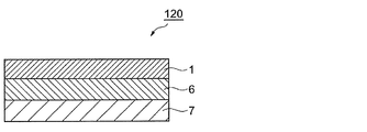
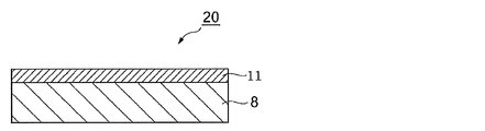
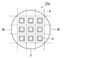
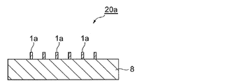
- FIG. 6 is an end view taken along line VI-VI in FIG. 5. It is a top view which shows one Embodiment of an adhesive layer pattern.
- FIG. 8 is an end view taken along line VIII-VIII in FIG. 7. It is a top view which shows one Embodiment of an adhesive layer pattern.
- FIG. 10 is an end view taken along line XX in FIG. 9.
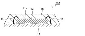
- 1 is a schematic cross-sectional view showing an embodiment of a semiconductor device of the present invention. It is a schematic cross section which shows other one Embodiment of the semiconductor device of this invention. It is a schematic cross section which shows other one Embodiment of the semiconductor device of this invention.
- the notation which does not describe substitution and non-substitution includes those having no substituent and those having a substituent.
- the “alkyl group” includes not only an alkyl group having no substituent (unsubstituted alkyl group) but also an alkyl group having a substituent (substituted alkyl group).
- active light means, for example, a bright line spectrum of a mercury lamp, far ultraviolet rays represented by excimer laser, extreme ultraviolet rays (EUV light), X-rays, electron beams, and the like.
- light means actinic rays or radiation.
- exposure in this specification is not only exposure with far-ultraviolet rays such as mercury lamps and excimer lasers, X-rays, EUV light, but also drawing with particle beams such as electron beams and ion beams. Are also included in the exposure.
- a numerical range expressed using “to” means a range including numerical values described before and after “to” as a lower limit value and an upper limit value.
- (meth) acrylate represents both and / or acrylate and methacrylate
- (meth) acryl represents both and / or acryl
- (meth) acryloyl represents both and / or acryloyl and methacryloyl.
- process is not limited to an independent process, and is included in the term if the intended action of the process is achieved even when it cannot be clearly distinguished from other processes. .
- the solid content concentration is the weight percentage of the weight of other components excluding the solvent with respect to the total weight of the composition. Moreover, solid content concentration says the density
- the weight average molecular weight is defined as a polystyrene converted value by GPC measurement.
- the weight average molecular weight (Mw) and the number average molecular weight (Mn) are, for example, HLC-8220 (manufactured by Tosoh Corporation) and TSKgelgSuper AWM-H (manufactured by Tosoh Corporation, 6) Unless otherwise stated, the eluent was measured using a 10 mmol / L lithium bromide NMP (N-methylpyrrolidinone) solution.
- the photosensitive resin composition of the present invention includes a polymer containing a repeating unit derived from an acid group-containing maleimide, a crosslinking agent, a photopolymerization initiator, and a thermal polymerization initiator. Since the photosensitive resin composition of this invention contains the polymer containing the repeating unit derived from an acid group containing maleimide, the hardened
- the photosensitive resin composition of the present invention contains a polymer containing a repeating unit derived from an acid group-containing maleimide (hereinafter also referred to as a maleimide polymer).
- the maleimide polymer used in the present invention preferably further contains a repeating unit derived from a vinyl compound.
- the polymer containing the repeating unit represented by the following general formula (1) and the repeating unit represented by the following general formula (2) is preferable.
- R 1 represents a hydrogen atom or a methyl group
- R 2 represents a hydrogen atom, an alkyl group, an alkoxy group, or an aryl group
- X represents an n + 1 valent linkage.
- A represents an acidic group
- n represents an integer of 1 to 10
- * represents a bond.
- R ⁇ 1 > represents a hydrogen atom or a methyl group, and a hydrogen atom is preferable.
- R 2 represents a hydrogen atom, an alkyl group, an alkoxy group or an aryl group.
- the alkyl group an alkyl group having 1 to 30 carbon atoms is preferable, and an alkyl group having 1 to 20 carbon atoms is preferable.
- the alkyl group may be linear, branched or cyclic.
- the alkoxy group an alkoxy group having 1 to 30 carbon atoms is preferable, and an alkoxy group having 1 to 20 carbon atoms is preferable.
- the alkoxy group may be linear, branched or cyclic.
- the aryl group is preferably an aryl group having 6 to 30 carbon atoms, more preferably an aryl group having 6 to 20 carbon atoms, and particularly preferably a phenyl group.
- R 2 in the general formula (1) is preferably a hydrogen atom or a phenyl group, particularly preferably a phenyl group.
- X represents an n + 1 valent linking group.
- the n + 1 valent linking group include an aliphatic hydrocarbon group, an aromatic hydrocarbon group, —O—, —NR ′ — (R ′ represents a hydrogen atom, an alkyl group which may have a substituent, or a substituent. And a group containing at least one selected from —SO 2 —, —CO—, —O—, and —S—. It is done. Of these, an aromatic hydrocarbon group is preferred from the viewpoint of heat resistance.
- the divalent linking group includes an alkylene group, an arylene group, —O—, —NR ′ — (R ′ has a hydrogen atom, an alkyl group which may have a substituent, or a substituent. And a group containing at least one selected from the group represented by —SO 2 —, —CO—, —O— and —S—.
- R ′ has a hydrogen atom, an alkyl group which may have a substituent, or a substituent.
- the alkylene group an alkylene group having 2 to 20 carbon atoms is preferable, and an alkylene group having 2 to 10 carbon atoms is more preferable.
- the arylene group an arylene group having 6 to 30 carbon atoms is preferable, and an arylene group having 6 to 20 carbon atoms is more preferable.
- the divalent linking group a phenylene group is particularly preferable.
- the trivalent linking group include a group in which one hydrogen atom is removed from the groups listed as examples of the divalent linking group.
- a trisubstituted benzene ring can be used.
- A represents an acidic group, and from the viewpoint of alkali developability, a carboxyl group, a phosphonic acid group, a phosphoric acid group, a sulfonic acid group, a hydroxyl group, and a sulfonamide group are preferable. From the viewpoint of developability, A sulfonamide group or a carboxyl group is more preferable, and a carboxyl group is particularly preferable.
- N represents an integer of 1 to 10, preferably 1 to 5, and more preferably 1 to 2.
- the ratio of the repeating unit represented by the general formula (1) to the repeating unit represented by the general formula (2) is 1: 1 to 6: 1 is preferred, 1: 1 to 4: 1 is more preferred, and 1: 1 to 3: 1 is even more preferred.
- the maleimide polymer used in the present invention includes a repeating unit other than the repeating unit represented by the general formula (1) and the repeating unit represented by the general formula (2) (hereinafter also referred to as other repeating units). You may go out.
- Other repeating units include, for example, unsaturated carboxylic acids (eg, acrylic acid, methacrylic acid, itaconic acid, crotonic acid, isocrotonic acid, maleic acid, etc.), esters of unsaturated carboxylic acids and alcohol compounds, unsaturated carboxylic acids Examples thereof include repeating units derived from an amide of an acid and an amine compound, an unsaturated carboxylic acid anhydride, and the like.
- the content of other repeating units in all repeating units is preferably 10 mol% or less, more preferably 5 mol% or less, and particularly preferably substantially not contained. “Substantially not containing” means that, for example, the content of other repeating units in all repeating units is preferably 1 mol% or less, more preferably 0.5 mol% or less, and no inclusion. Is particularly preferred.
- maleimide polymer containing the repeating unit represented by the general formula (1) and the repeating unit represented by the following general formula (2) are described below, but the present invention is not limited thereto. It is not something. These can be used alone or in admixture of two or more.
- Me represents a methyl group.
- the polymer containing the repeating unit represented by the general formula (1) and the repeating unit represented by the general formula (2) can be synthesized by copolymerizing a vinyl compound and an acidic group-containing maleimide.
- a vinyl compound and an acidic group-containing maleimide can be obtained by radical copolymerization of, for example, a vinyl compound and an acidic group-containing maleimide. That is, it can be synthesized by mixing a vinyl compound and an acidic group-containing maleimide in an organic solvent at an arbitrary ratio, and further adding and reacting a radical polymerization initiator or a chain transfer agent as necessary.
- the acidic group-containing maleimide can be obtained, for example, by imidization using maleic anhydride and an acidic group-containing amine compound.
- it can also be obtained by radical copolymerization of a vinyl compound and maleic anhydride and then imidization using an amine compound. At this time, it can be synthesized by adding a base, an acid, an acid anhydride or the like, if necessary.
- the vinyl compound is not particularly limited as long as it is a compound having a group having an ethylenically unsaturated bond.
- ⁇ -olefin compounds, conjugated diene compounds, aromatic vinyl compounds, vinyl ether compounds, vinyl ester compounds, (meth) An acrylate compound, a (meth) acrylamide compound and the like are preferably used.
- aromatic vinyl compounds are preferable, and aromatic vinyl compounds are more preferably used.
- the ⁇ -olefin is preferably an ⁇ -olefin having 2 to 30 carbon atoms, and examples thereof include ethylene, propylene, 1-butene, 1-hexene, 1-octene, 1-decene, 1-dodecene and 1-octadecene. It is done. Of these, ethylene is preferably used.
- the aromatic vinyl compound include styrene, alkyl styrene, aryl styrene, halogenated styrene, alkoxy styrene, vinyl benzoate, and the like. Of these, styrene is preferably used.
- alkyl styrene examples include o-methyl styrene, m-methyl styrene, p-methyl styrene, o-ethyl styrene, m-ethyl styrene, p-ethyl styrene, on-propyl styrene, mn-propyl.
- Styrene pn-propyl styrene, o-isopropyl styrene, m-isopropyl styrene, p-isopropyl styrene, mn-butyl styrene, pn-butyl styrene, p-tert-butyl styrene, 4-butenyl styrene 2,4-dimethylstyrene, 2,5-dimethylstyrene, 3,5-dimethylstyrene, mesitylstyrene and the like.
- arylstyrene include p-phenylstyrene.
- halogenated styrene examples include o-fluorostyrene, m-fluorostyrene, p-fluorostyrene, o-chlorostyrene, m-chlorostyrene, p-chlorostyrene, o-bromostyrene, m-bromostyrene, p -Bromostyrene, o-methyl-p-fluorostyrene and the like.
- alkoxystyrene include o-methoxystyrene, m-methoxystyrene, p-methoxystyrene and the like.
- acidic group-containing maleimide a compound having a structure represented by the general formula (2a) can be used.
- X represents an n + 1 valent linking group
- A represents an acidic group
- n represents an integer of 1 to 10
- * represents a linking group
- X, A and n in the general formula (2a) have the same meanings as X, A and n in the general formula (2), and preferred ranges are also the same.
- the acid value of the maleimide polymer is preferably 50 mgKOH / g or more from the viewpoint of developability, more preferably 80 to 300 mgKOH / g, and particularly preferably 100 to 250 mgKOH / g. By setting it as such a range, the effect of this invention is exhibited more effectively.
- the weight loss rate at 300 ° C. of the maleimide polymer when heated at 20 ° C./min is preferably 5% or less, more preferably 3% or less, and preferably 1% or less. Particularly preferred. By setting it as such a range, heat resistance improves more.
- the weight average molecular weight of the maleimide polymer is preferably 2,000 to 1,000,000, more preferably 3,000 to 500,000, and even more preferably 5,000 to 100,000 in terms of polystyrene by gel permeation chromatography (GPC). If it is 2000 or more, heat resistance will become more favorable, and if it is 1000000 or less, developability will become more favorable.
- the photosensitive resin composition of the present invention preferably contains the maleimide polymer in an amount of 30 to 90% by mass, more preferably 40 to 90% by mass, based on the total solid content of the photosensitive resin composition. 50 to 90% by mass is particularly preferable.
- the photosensitive resin composition of the present invention contains a crosslinking agent.
- the cross-linking agent is a compound having two or more polymerizable groups, and a known compound that can be polymerized by the action of actinic rays, radiation, light, heat, radicals or acids can be used. Such compounds are widely known in the industrial field, and can be used without particular limitation in the present invention. These may be any of chemical forms such as monomers, prepolymers, oligomers or mixtures thereof and multimers thereof.
- the crosslinking agent in the present invention is a compound different from the maleimide polymer described above. That is, the crosslinking agent of the present invention is a compound that does not contain a repeating unit derived from an acid group-containing maleimide.
- the monomer type cross-linking agent (hereinafter also referred to as polymerizable monomer) is a compound different from the polymer compound.
- the polymerizable monomer is typically a low molecular compound, preferably a low molecular compound having a molecular weight of 2000 or less, more preferably a low molecular compound having a molecular weight of 1500 or less, and a low molecular compound having a molecular weight of 900 or less. More preferably it is.
- the molecular weight of the polymerizable monomer is usually 100 or more.
- the polymerizable group is preferably a functional group that can undergo an addition polymerization reaction, for example.
- the functional group capable of undergoing addition polymerization include a group having an ethylenically unsaturated bond, an amino group, and an epoxy group.
- the polymerizable group may be a functional group capable of generating a radical upon irradiation with light, and examples of such a polymerizable group include a thiol group and a halogen group.
- the polymerizable group is preferably a group having an ethylenically unsaturated bond.
- the crosslinking agent is preferably a compound having a group having an ethylenically unsaturated bond.
- the crosslinking agent preferably contains at least one bifunctional or higher functional crosslinking agent containing two or more polymerizable groups, and preferably contains at least one trifunctional or higher functional crosslinking agent. More preferred. Among these, a bifunctional or higher functional crosslinking agent having two or more groups having an ethylenically unsaturated bond is particularly preferable because the developability and heat resistance can be further improved.
- the photosensitive resin composition of this invention may contain the compound which has an epoxy group as a polymeric group, since the developability and heat resistance can be improved more, the epoxy in 100 mass parts of crosslinking agents is used.
- the content of the group-containing compound is preferably 10% by mass or less, more preferably 5% by mass or less, and particularly preferably substantially not contained.
- substantially not containing, for example, the content of the compound having an epoxy group is preferably 1% by mass or less, more preferably 0.5% by mass or less, particularly preferably 0.1% by mass or less, and not contained. It is particularly preferred.
- the crosslinking agent include a radical polymerizable compound (B1) and an ion polymerizable compound (B2).
- Radically polymerizable compound (B1) examples include a (meth) acrylamide compound (B11) having 3 to 35 carbon atoms, a (meth) acrylate compound (B12) having 4 to 35 carbon atoms, and an aromatic vinyl compound having 6 to 35 carbon atoms. (B13), vinyl ether compounds having 3 to 20 carbon atoms (B14), and other radical polymerizable compounds (B15).
- a radically polymerizable compound (B1) may be used individually by 1 type, or may use 2 or more types together. Further, if necessary, a polymerization inhibitor such as hydroquinone or methyl ether hydroquinone may be used in combination.
- Examples of the (meth) acrylate compound (B12) having 4 to 35 carbon atoms include the following difunctional to hexafunctional (meth) acrylates.
- EO represents ethylene oxide
- PO represents propylene oxide.
- Bifunctional (meth) acrylates include 1,4-butanedi (meth) acrylate, 1,6-hexanediacrylate, polypropylene diacrylate, 1,6-hexanediol di (meth) acrylate, and 1,10-decanedioldi (Meth) acrylate, neopentyl diacrylate, neopentyl glycol di (meth) acrylate, 2,4-dimethyl-1,5-pentanediol di (meth) acrylate, butylethylpropanediol (meth) acrylate, ethoxylated cyclohexanemethanol Di (meth) acrylate, polyethylene glycol di (meth) acrylate, oligoethylene glycol di (meth) acrylate, ethylene glycol di (meth) acrylate, 2-ethyl-2-butyl-butanediol di (meth) Acrylate,
- Trifunctional (meth) acrylates include trimethylolpropane tri (meth) acrylate, trimethylolethane tri (meth) acrylate, trimethylolpropane alkylene oxide modified tri (meth) acrylate, pentaerythritol tri (meth) acrylate, di Pentaerythritol tri (meth) acrylate, trimethylolpropane tri ((meth) acryloyloxypropyl) ether, isocyanuric acid alkylene oxide modified tri (meth) acrylate, dipentaerythritol tri (meth) acrylate propionate, tri ((meta ) Acryloyloxyethyl) isocyanurate, hydroxypivalaldehyde-modified dimethylolpropane tri (meth) acrylate, sorbitol tri (meth) acrylate DOO, propoxylated trimethylolpropane tri (meth) acrylate
- Tetrafunctional (meth) acrylates include pentaerythritol tetra (meth) acrylate, sorbitol tetra (meth) acrylate, ditrimethylolpropane tetra (meth) acrylate, propionate dipentaerythritol tetra (meth) acrylate and ethoxylated pentaerythritol tetra. (Meth) acrylate etc. are mentioned.
- pentafunctional (meth) acrylates examples include sorbitol penta (meth) acrylate and dipentaerythritol penta (meth) acrylate.
- hexafunctional (meth) acrylates examples include dipentaerythritol hexa (meth) acrylate, sorbitol hexa (meth) acrylate, phosphazene alkylene oxide modified hexa (meth) acrylate, and caprolactone modified dipentaerythritol hexa (meth) acrylate. It is done.
- Examples of the vinyl ether compound (B14) having 3 to 35 carbon atoms include the following polyfunctional vinyl ethers.
- polyfunctional vinyl ether examples include ethylene glycol divinyl ether, diethylene glycol divinyl ether, polyethylene glycol divinyl ether, propylene glycol divinyl ether, butylene glycol divinyl ether, hexanediol divinyl ether, bisphenol A alkylene oxide divinyl ether, bisphenol F alkylene oxide divinyl ether.
- Divinyl ethers such as: trimethylolethane trivinyl ether, trimethylolpropane trivinyl ether, ditrimethylolpropane tetravinyl ether, glycerin trivinyl ether, pentaerythritol tetravinyl ether, dipentaerythritol pentavinyl ether, dipentaerythritol hexabi Ether, ethylene oxide-added trimethylolpropane trivinyl ether, propylene oxide-added trimethylolpropane trivinyl ether, ethylene oxide-added ditrimethylolpropane tetravinyl ether, propylene oxide-added ditrimethylolpropane tetravinyl ether, ethylene oxide-added pentaerythritol tetravinyl ether, propylene oxide-added pentaerythritol te
- radical polymerizable compounds (B15) include vinyl ester compounds (such as vinyl acetate, vinyl propionate and vinyl versatate), allyl ester compounds (such as allyl acetate), halogen-containing monomers (vinylidene chloride, vinyl chloride, etc.) ) And olefin compounds (ethylene and propylene, etc.).
- (meth) acrylamide compound (B11) and (meth) acrylate compound (B12) are preferable from the viewpoint of polymerization rate, and (meth) acrylate compound (B12) is particularly preferable.
- Ion polymerizable compound (B2) Examples of the ion polymerizable compound (B2) include an epoxy compound (B21) having 3 to 20 carbon atoms and an oxetane compound (B22) having 4 to 20 carbon atoms.
- Examples of the epoxy compound having 3 to 20 carbon atoms (B21) include the following polyfunctional epoxy compounds.
- polyfunctional epoxy compound examples include bisphenol A diglycidyl ether, bisphenol F diglycidyl ether, bisphenol S diglycidyl ether, brominated bisphenol A diglycidyl ether, brominated bisphenol F diglycidyl ether, and brominated bisphenol S diglycidyl ether.
- Epoxy novolac resin hydrogenated bisphenol A diglycidyl ether, hydrogenated bisphenol F diglycidyl ether, hydrogenated bisphenol S diglycidyl ether, 3,4-epoxycyclohexylmethyl-3 ', 4'-epoxycyclohexanecarboxylate, 2- (3,4-epoxycyclohexyl-5,5-spiro-3,4-epoxy) cyclohexane-meta-dioxane, bis (3,4-epoxycyclohexyl) Methyl) adipate, vinylcyclohexene oxide, 4-vinylepoxycyclohexane, bis (3,4-epoxy-6-methylcyclohexylmethyl) adipate, 3,4-epoxy-6-methylcyclohexyl-3 ′, 4′-epoxy-6 '-Methylcyclohexanecarboxylate, methylenebis (3,4-epoxycyclo
- aromatic epoxides and alicyclic epoxides are preferable, and alicyclic epoxides are particularly preferable from the viewpoint of excellent polymerization rate.
- Examples of the oxetane compound (B22) having 4 to 20 carbon atoms include compounds having 2 to 6 oxetane rings.
- Examples of the compound having 2 to 6 oxetane rings include 3,7-bis (3-oxetanyl) -5-oxa-nonane, 3,3 ′-(1,3- (2-methylenyl) propanediylbis ( Oxymethylene)) bis- (3-ethyloxetane), 1,4-bis [(3-ethyl-3-oxetanylmethoxy) methyl] benzene, 1,2-bis [(3-ethyl-3-oxetanylmethoxy) methyl ] Ethane, 1,3-bis [(3-ethyl-3-oxetanylmethoxy) methyl] propane, ethylene glycol bis (3-ethyl-3-oxetanylmethyl) ether, dicyclopentenylbis (3-ethyl-3-oxetanyl) Methyl) ether, triethylene glycol bis (3-ethyl-3-oxetanylmethyl) ether,
- the cross-linking agent is preferably a compound having two or more polymerizable groups selected from an epoxy group, an acrylic group, a methacryl group, an allyl group and a styryl group, and selected from an acrylic group, a methacryl group, an allyl group and a styryl group. More preferably, the compound having two or more polymerizable groups is one or more, having two or more polymerizable groups selected from an acryl group, a methacryl group, an allyl group, and a styryl group, and the following parts: More preferred are compounds having a structure. When the crosslinking agent has the following partial structure, the heat resistance can be further improved.
- cross-linking agents examples include A-9300, A-TMPT, A-TMMT, AD-TMP, A-DPH, A-BPE-4, 4G (manufactured by Shin-Nakamura Chemical Co., Ltd., (meth) acrylate compounds) Etc.
- the content of the crosslinking agent in the photosensitive resin composition of the present invention is preferably 5 to 75% by mass with respect to the total solid content of the photosensitive resin composition from the viewpoint of good developability, adhesive strength, and heat resistance. 10 to 70 mass% is more preferable, and 10 to 60 mass% is still more preferable.
- the photosensitive resin composition of the present invention may contain a monofunctional polymerizable compound having one polymerizable group.
- a monofunctional polymerizable compound having one polymerizable group it is synonymous with the range demonstrated by the crosslinking agent mentioned above, and its preferable range is also the same.
- the monofunctional polymerizable compound include monofunctional (meth) acrylates, monofunctional (meth) acrylamides, aromatic vinyl compounds, monofunctional vinyl ethers, compounds having one oxetane ring, and the like.
- Monofunctional (meth) acrylates include ethyl (meth) acrylate, hexyl (meth) acrylate, 2-ethylhexyl (meth) acrylate, tert-octyl (meth) acrylate, isoamyl (meth) acrylate, decyl (meth) acrylate, isodecyl (Meth) acrylate, stearyl (meth) acrylate, isostearyl (meth) acrylate, cyclohexyl (meth) acrylate, 4-n-butylcyclohexyl (meth) acrylate, bornyl (meth) acrylate, isobornyl (meth) acrylate, benzyl ( (Meth) acrylate, 2-ethylhexyl diglycol (meth) acrylate, butoxyethyl (meth) acrylate, 2-chloroethyl (meth) acryl
- Examples of monofunctional (meth) acrylamide compounds include (meth) acrylamide, N-methyl (meth) acrylamide, N-ethyl (meth) acrylamide, N-propyl (meth) acrylamide, and Nn-butyl (meth) acrylamide. , Nt-butyl (meth) acrylamide, N-butoxymethyl (meth) acrylamide, N-isopropyl (meth) acrylamide, N-methylol (meth) acrylamide, N, N-dimethyl (meth) acrylamide, N, N- Examples include diethyl (meth) acrylamide and (meth) acryloylmorpholine.
- Examples of the monofunctional aromatic vinyl compound (B13) include vinyl thiophene, vinyl furan, vinyl pyridine, styrene, methyl styrene, trimethyl styrene, ethyl styrene, isopropyl styrene, chloromethyl styrene, methoxy styrene, acetoxy styrene, chloro styrene, dichloro.
- Styrene bromostyrene, vinyl benzoic acid methyl ester, 3-methylstyrene, 4-methylstyrene, 3-ethylstyrene, 4-ethylstyrene, 3-propylstyrene, 4-propylstyrene, 3-butylstyrene, 4-butylstyrene 3-hexylstyrene, 4-hexylstyrene, 3-octylstyrene, 4-octylstyrene, 3- (2-ethylhexyl) styrene, 4- (2-ethylhexyl) styrene, allylstyrene, isopropyl Nirusuchiren, butenylstyrene, octenyl styrene, 4-t-butoxycarbonyl styrene, 4-methoxystyrene and 4-t-butoxy
- Examples of the monofunctional vinyl ether include methyl vinyl ether, ethyl vinyl ether, propyl vinyl ether, n-butyl vinyl ether, t-butyl vinyl ether, 2-ethylhexyl vinyl ether, n-nonyl vinyl ether, lauryl vinyl ether, cyclohexyl vinyl ether, cyclohexyl methyl vinyl ether, 4-methyl Cyclohexylmethyl vinyl ether, benzyl vinyl ether, dicyclopentenyl vinyl ether, 2-dicyclopentenoxyethyl vinyl ether, methoxyethyl vinyl ether, ethoxyethyl vinyl ether, butoxyethyl vinyl ether, methoxyethoxyethyl vinyl ether, ethoxyethoxyethyl vinyl ether, methoxypolyethylene glycol vinyl ether , Tetrahydrofurfuryl vinyl ether, 2-hydroxyethyl vinyl ether, 2-hydroxypropyl
- Examples of the monofunctional epoxy compound include phenyl glycidyl ether, p-tert-butylphenyl glycidyl ether, butyl glycidyl ether, 2-ethylhexyl glycidyl ether, allyl glycidyl ether, 1,2-butylene oxide, and 1,3-butadiene monooxide.
- Examples of the compound having one oxetane ring include 3-ethyl-3-hydroxymethyloxetane, 3- (meth) allyloxymethyl-3-ethyloxetane, (3-ethyl-3-oxetanylmethoxy) methylbenzene, 4 -Fluoro- [1- (3-ethyl-3-oxetanylmethoxy) methyl] benzene, 4-methoxy- [1- (3-ethyl-3-oxetanylmethoxy) methyl] benzene, [1- (3-ethyl-3 -Oxetanylmethoxy) ethyl] phenyl ether, isobutoxymethyl (3-ethyl-3-oxetanylmethyl) ether, isobornyloxyethyl (3-ethyl-3-oxetanylmethyl) ether, isobornyl (3-ethyl-3-oxet
- the content of the monofunctional polymerizable compound is preferably 0.1 to 200 parts by mass with respect to 100 parts by mass of the crosslinking agent. 100 parts by mass is more preferable. Only one type of monofunctional polymerizable compound may be used, or two or more types may be used in combination. When using 2 or more types together, it is preferable that the total is the said content.
- the photosensitive resin composition of the present invention contains a photopolymerization initiator.
- the photosensitive resin composition of the present invention contains a photopolymerization initiator
- the photosensitive resin composition is applied to a semiconductor wafer or the like to form a layered photosensitive resin composition layer, and then irradiated with light.
- curing by radicals or acids occurs, and the adhesiveness in the light irradiation part can be reduced.
- light irradiation is performed through, for example, a photomask, there is an advantage that regions having different adhesive forces can be easily created in accordance with the photomask pattern.
- the photopolymerization initiator is not particularly limited as long as it has the ability to initiate the polymerization reaction (crosslinking reaction) of the crosslinking agent, and can be appropriately selected from known photopolymerization initiators. For example, those having photosensitivity to visible light from the ultraviolet region are preferable. Further, it may be an activator that generates some active radicals by generating some action with the photoexcited sensitizer. A compound that generates a radical or an acid upon irradiation with light is preferred.
- the photopolymerization initiator preferably contains at least one compound having a molecular extinction coefficient of at least about 50 within a range of about 300 nm to 800 nm (preferably 330 nm to 500 nm).
- halogenated hydrocarbon derivatives for example, those having a triazine skeleton, those having an oxadiazole skeleton, those having a trihalomethyl group
- acylphosphine compounds such as acylphosphine oxide, hexaarylbiimidazoles, oxime derivatives, etc.
- Oxime compounds, organic peroxides, thio compounds, ketone compounds, aromatic onium salts, ketoxime ethers, aminoacetophenone compounds, hydroxyacetophenone, azo compounds, azide compounds, metallocene compounds, organoboron compounds, iron arene complexes, etc. Can be mentioned.
- halogenated hydrocarbon compounds having a triazine skeleton examples include those described in Wakabayashi et al., Bull. Chem. Soc. Japan, 42, 2924 (1969), a compound described in British Patent No. 1388492, a compound described in JP-A-53-133428, a compound described in German Patent No. 3337024, F.I. C. J. Schaefer et al. Org. Chem. 29, 1527 (1964), compound described in JP-A-62-258241, compound described in JP-A-5-281728, compound described in JP-A-5-34920, US Pat. No. 4,221,976 And the compounds described in the book.
- Examples of the compounds described in US Pat. No. 4,221,976 include compounds having an oxadiazole skeleton (for example, 2-trichloromethyl-5-phenyl-1,3,4-oxadiazole, 2-trichloro Methyl-5- (4-chlorophenyl) -1,3,4-oxadiazole, 2-trichloromethyl-5- (1-naphthyl) -1,3,4-oxadiazole, 2-trichloromethyl-5 (2-naphthyl) -1,3,4-oxadiazole, 2-tribromomethyl-5-phenyl-1,3,4-oxadiazole, 2-tribromomethyl-5- (2-naphthyl)- 1,3,4-oxadiazole; 2-trichloromethyl-5-styryl-1,3,4-oxadiazole, 2-trichloromethyl-5- (4-chlorostyryl) 1,3,4-oxadiazole, 2-trichloromethyl-5-
- photopolymerization initiators other than those mentioned above, polyhalogen compounds (for example, 9-phenylacridine, 1,7-bis (9,9′-acridinyl) heptane, etc.), N-phenylglycine, etc.
- polyhalogen compounds for example, 9-phenylacridine, 1,7-bis (9,9′-acridinyl) heptane, etc.
- N-phenylglycine etc.
- acylphosphine oxides for example, bis (2,4 , 6-Trimethylbenzoyl) -phenylphos Zinc oxide, bis (2,6-dimethoxybenzoyl) -2,4,4-trimethyl-pentylphenylphosphine oxide, Lucirin TPO, etc.
- metallocenes for example, bis ( ⁇ 5-2,4-cyclopentadien-1-yl)- Bis (2,6-difluoro-3- (1H-pyrrol-1-yl) -phenyl) titanium, ⁇ 5-cyclopentadienyl- ⁇ 6-cumenyl-iron (1 +)-hexafluorophosphate (1-), etc.
- Examples thereof include compounds described in JP-A-53-133428, JP-B-57-1819, JP-A-57-60
- ketone compound examples include benzophenone, 2-methylbenzophenone, 3-methylbenzophenone, 4-methylbenzophenone, 4-methoxybenzophenone, 2-chlorobenzophenone, 4-chlorobenzophenone, 4-bromobenzophenone, 2-carboxybenzophenone, 2 -Ethoxycarbonylbenzophenone, benzophenone tetracarboxylic acid or its tetramethyl ester, 4,4'-bis (dialkylamino) benzophenones (eg, 4,4'-bis (dimethylamino) benzophenone, 4,4'-bisdicyclohexylamino ) Benzophenone, 4,4′-bis (diethylamino) benzophenone, 4,4′-bis (dihydroxyethylamino) benzophenone, 4-methoxy-4′-dimethylaminoben Phenone, 4,4'-dimethoxybenzophenone, 4-dimethylamino
- hydroxyacetophenone compounds As the photopolymerization initiator, hydroxyacetophenone compounds, aminoacetophenone compounds, and acylphosphine compounds can also be suitably used. More specifically, for example, aminoacetophenone initiators described in JP-A-10-291969 and acylphosphine oxide initiators described in Japanese Patent No. 4225898 can also be used.
- hydroxyacetophenone-based initiator IRGACURE-184, DAROCUR-1173, IRGACURE-500, IRGACURE-2959, IRGACURE-127 (trade names: all manufactured by BASF) can be used.
- aminoacetophenone initiator commercially available products IRGACURE-907, IRGACURE-369, and IRGACURE-379 (trade names: all manufactured by BASF) can be used.
- aminoacetophenone-based initiator compounds described in JP-A-2009-191179 whose absorption wavelength is matched with a long wave light source of 365 nm or 405 nm can also be used.
- acylphosphine initiator commercially available products such as IRGACURE-819 and DAROCUR-TPO (trade names: both manufactured by BASF) can be used.
- More preferable examples of the photopolymerization initiator include oxime compounds.
- Specific examples of the oxime initiator include compounds described in JP-A No. 2001-233842, compounds described in JP-A No. 2000-80068, and compounds described in JP-A No. 2006-342166.
- Examples of the oxime compound that can be suitably used as a photopolymerization initiator in the present invention include 3-benzoyloxyiminobutan-2-one, 3-acetoxyiminobutan-2-one, and 3-propionyloxyiminobutane-2- ON, 2-acetoxyiminopentan-3-one, 2-acetoxyimino-1-phenylpropan-1-one, 2-benzoyloxyimino-1-phenylpropan-1-one, 3- (4-toluenesulfonyloxy) ) Iminobutan-2-one and 2-ethoxycarbonyloxyimino-1-phenylpropan-1-one.
- oxime ester compounds include J.M. C. S. Perkin II (1979) pp. 1653-1660), J.M. C. S. Perkin II (1979) pp. 156-162, Journal of Photopolymer Science and Technology (1995), pp. 156-162. Examples thereof include compounds described in 202-232, JP-A No. 2000-66385, JP-A No. 2000-80068, JP-T 2004-534797, JP-A No. 2006-342166, and the like.
- IRGACURE-OXE01 manufactured by BASF
- IRGACURE-OXE02 manufactured by BASF
- N-1919 manufactured by ADEKA
- oxime ester compounds other than those described above compounds described in JP-T-2009-519904 in which oxime is linked to carbazole N-position, compounds described in US Pat. No. 7,626,957 in which a hetero substituent is introduced into the benzophenone moiety, A compound described in Japanese Patent Application Laid-Open No. 2010-15025 and US Patent Publication No. 2009-292039 in which a nitro group is introduced at the dye moiety, a ketoxime compound described in International Patent Publication No. 2009-131189, the triazine skeleton and the oxime skeleton are the same A compound described in US Pat. No. 7,556,910 contained in the molecule, a compound described in JP 2009-221114 A having an absorption maximum at 405 nm and good sensitivity to a g-ray light source may be used.
- cyclic oxime compounds described in JP-A-2007-231000 and JP-A-2007-322744 can also be suitably used for the cyclic oxime compounds described in JP-A-2007-231000 and JP-A-2007-322744.
- cyclic oxime compounds in particular, cyclic oxime compounds fused to carbazole dyes described in JP2010-32985A and JP2010-185072A have high light absorptivity and high sensitivity. preferable.
- the compounds described in JP-A-2009-242469 having an unsaturated bond at a specific site of the oxime compound can be preferably used because high sensitivity can be achieved by regenerating the active radical from the polymerization inert radical. it can.
- an oxime compound having a specific substituent as disclosed in JP-A-2007-269979 and an oxime compound having a thioaryl group as described in JP-A-2009-191061 are exemplified.
- Photopolymerization initiators are trihalomethyltriazine compounds, benzyldimethylketal compounds, ⁇ -hydroxyketone compounds, ⁇ -aminoketone compounds, acylphosphine compounds, phosphine oxide compounds, metallocene compounds, oxime compounds, triallyls from the viewpoint of exposure sensitivity. Selected from the group consisting of imidazole dimers, onium compounds, benzothiazole compounds, benzophenone compounds, acetophenone compounds and derivatives thereof, cyclopentadiene-benzene-iron complexes and salts thereof, halomethyloxadiazole compounds, and 3-aryl substituted coumarin compounds. Compounds are preferred.
- trihalomethyltriazine compounds More preferred are trihalomethyltriazine compounds, ⁇ -aminoketone compounds, acylphosphine compounds, phosphine oxide compounds, oxime compounds, triallylimidazole dimers, onium compounds, benzophenone compounds, and acetophenone compounds.
- oxime compounds Particularly preferred are oxime compounds.
- a compound that generates an acid having a pKa of 4 or less can be preferably used, and a compound that generates an acid having a pKa of 3 or less is more preferable.
- the acid-generating compound examples include trichloromethyl-s-triazines, sulfonium salts and iodonium salts, quaternary ammonium salts, diazomethane compounds, imide sulfonate compounds, and oxime sulfonate compounds. Among these, it is preferable to use an oxime sulfonate compound from the viewpoint of high sensitivity.
- These acid generators can be used singly or in combination of two or more. Specific examples include acid generators described in paragraphs [0073] to [0095] of JP2012-8223A.
- a known method can be used for the molar extinction coefficient of the photopolymerization initiator. Specifically, for example, it is preferable to measure at a concentration of 0.01 g / L using an ultraviolet-visible spectrophotometer (Carry-5 spctrophotometer manufactured by Varian) using an ethyl acetate solvent.
- the photopolymerization initiator is preferably contained in an amount of 0.1 to 50% by mass, preferably 0.1 to 30% by mass, based on the total solid content of the photosensitive resin composition.
- the content is more preferably 0.1 to 20% by mass.
- the photosensitive resin composition of the present invention preferably contains 0.1 to 30 parts by mass, more preferably 0.2 to 20 parts by mass of the photopolymerization initiator with respect to 100 parts by mass of the crosslinking agent.
- the content is preferably 1 to 20 parts by mass. Only one photopolymerization initiator may be used, or two or more photopolymerization initiators may be used in combination. When using 2 or more types together, it is preferable that the total is the said content.
- the photosensitive resin composition of the present invention contains a thermal polymerization initiator. Since the photosensitive resin composition of the present invention contains a thermal polymerization initiator, the photosensitive resin composition is applied to a semiconductor wafer or the like to form a layered photosensitive resin composition layer, and then the adherend is bonded. By heating, the photosensitive resin composition layer becomes more tough and suppresses the cohesive failure of the photosensitive resin composition layer that is likely to occur when the adherend is subjected to mechanical or chemical treatment. it can. That is, the adhesiveness in the photosensitive resin composition layer can be improved. Moreover, sclerosis
- hardenability can be improved by using a photoinitiator and a thermal-polymerization initiator together.
- the one-minute half-life temperature of the thermal polymerization initiator is preferably 120 to 300 ° C, more preferably 150 to 250 ° C, still more preferably 150 to 230 ° C, from the viewpoint of stability and curability of the photosensitive resin composition. 170 to 200 ° C. is particularly preferable.
- the half-life temperature for 1 minute of the thermal polymerization initiator is equal to or higher than the above lower limit, the film is not excessively cured when dried and the developability is good. If the 1-minute half-life temperature of a thermal-polymerization initiator is below the said lower limit, sclerosis
- the molecular weight of the thermal polymerization initiator is preferably 100 or more, more preferably 150 or more, further preferably 200 or more, and particularly preferably 250 or more, from the viewpoint of volatility.
- the upper limit is preferably 1000 or less, and more preferably 500 or less. If the molecular weight of the thermal polymerization initiator is not less than the above lower limit, volatilization of the thermal polymerization initiator during drying of the coating film can be effectively suppressed, and curability is good.
- thermal polymerization initiator a compound that generates radicals by heat (hereinafter also simply referred to as a thermal radical generator) or a compound that generates acids by heat (hereinafter also simply referred to as a thermal acid generator) is used. Can do.
- a thermal radical generator is preferable. Since the thermal radical generator can promote radical polymerization of ethylenically unsaturated groups, when a compound containing a group having an ethylenically unsaturated bond is used as the crosslinking agent, the polymerization reaction of the crosslinking agent is more effective. And can be cured in a shorter time.
- the reaction in which the polymerization reaction is initiated and accelerated by the thermal acid generator is epoxy ring-opening polymerization. Since ring-opening polymerization of epoxy has a slower polymerization rate than radical polymerization, curability may not be sufficiently promoted.
- Thermal Radical Generator a known thermal radical generator can be used.
- the thermal radical generator is a compound that generates radicals by heat energy and initiates or accelerates the polymerization reaction of the crosslinking agent.
- Thermal radical generators include aromatic ketones, onium salt compounds, organic peroxides, thio compounds, hexaarylbiimidazole compounds, ketoxime ester compounds, borate compounds, azinium compounds, metallocene compounds, active ester compounds, carbon halogens Examples thereof include a compound having a bond and an azo compound. Among these, an organic peroxide or an azo compound is more preferable, and an organic peroxide is particularly preferable.
- thermal acid generator is, for example, a compound that generates a low nucleophilic acid such as sulfonic acid, carboxylic acid, or disulfonylimide by heating.
- the acid generated from the thermal acid generator is preferably an acid having a pKa of 2 or less.
- a sulfonic acid, an alkyl carboxylic acid substituted with an electron withdrawing group, an aryl carboxylic acid, disulfonylimide, or the like is preferable.
- the electron withdrawing group examples include a halogen atom such as a fluorine atom, a haloalkyl group such as a trifluoromethyl group, a nitro group, and a cyano group.
- a sulfonic acid ester that does not substantially generate an acid by irradiation with actinic rays or radiation and generates an acid by heat. It is determined that there is no change in the spectrum by measuring infrared absorption (IR) spectrum and nuclear magnetic resonance (NMR) spectrum before and after the exposure of the compound that the acid is not substantially generated by irradiation with actinic ray or radiation. can do.
- the molecular weight of the sulfonic acid ester is preferably 230 to 1,000, more preferably 230 to 800.
- a commercially available one may be used, or one synthesized by a known method may be used.
- the sulfonic acid ester can be synthesized, for example, by reacting a sulfonyl chloride or a sulfonic acid anhydride with a corresponding polyhydric alcohol under basic conditions. Examples of commercially available products include cyclohexyl p-toluenesulfonate (manufactured by Tokyo Chemical Industry Co., Ltd.).
- the photosensitive resin composition of the present invention preferably contains a thermal polymerization initiator in an amount of 0.01 to 50% by mass, preferably 0.1 to 20% by mass, based on the total solid content of the photosensitive resin composition.
- the content is more preferably 0.5 to 10% by mass.
- the photosensitive resin composition of the present invention preferably contains 1 to 500 parts by mass, more preferably 10 to 200 parts by mass of the thermal polymerization initiator with respect to 100 parts by mass of the photopolymerization initiator.
- the photosensitive resin composition of the present invention preferably contains 0.1 to 30 parts by mass, more preferably 0.2 to 20 parts by mass of the thermal polymerization initiator with respect to 100 parts by mass of the crosslinking agent.
- the content is preferably 0.5 to 20 parts by mass, more preferably 1 to 20 parts by mass. Only one type of thermal polymerization initiator may be used, or two or more types may be used in combination. When using 2 or more types together, it is preferable that the total is the said content.
- the ratio of the combination of the photopolymerization initiator and the thermal polymerization initiator is preferably 0.1 to 10: 1, more preferably 0.2 to 5: 1, and still more preferably 0.3 to 3 in terms of mass ratio. : 1.
- the photosensitive resin composition of the present invention can contain a solvent.
- a known solvent can be used without limitation.
- the organic solvent include esters, ethers, ketones, amides, alcohols, hydrocarbons and the like.
- esters include ethyl acetate, n-butyl acetate, isobutyl acetate, amyl formate, isoamyl acetate, isobutyl acetate, butyl propionate, isopropyl butyrate, ethyl butyrate, butyl butyrate, methyl lactate, ethyl lactate, alkyl oxyacetate (Example: methyl oxyacetate, ethyl oxyacetate, butyl oxyacetate (eg, methyl methoxyacetate, ethyl methoxyacetate, butyl methoxyacetate, methyl ethoxyacetate, ethyl ethoxyacetate)), 3-oxypropionic acid alkyl esters (example : Methyl 3-oxypropionate, ethyl 3-oxypropionate, etc.
- 2 -Oxypropio Acid alkyl esters eg, methyl 2-oxypropionate, ethyl 2-oxypropionate, propyl 2-oxypropionate, etc.
- ethers include diethylene glycol dimethyl ether, tetrahydrofuran, ethylene glycol monomethyl ether, ethylene glycol monoethyl ether, methyl cellosolve acetate, ethyl cellosolve acetate, diethylene glycol monomethyl ether, diethylene glycol monoethyl ether, diethylene glycol monobutyl ether, propylene glycol monomethyl ether, propylene Examples include glycol monomethyl ether acetate, propylene glycol monoethyl ether acetate, and propylene glycol monopropyl ether acetate.
- ketones include methyl amyl ketone, methyl ethyl ketone, cyclopentanone, cyclohexanone, 2-heptanone, and 3-heptanone.
- amides include N, N-dimethylformamide, N, N-dimethylacetamide, N-methyl-2-pyrrolidone and the like.
- alcohols examples include methanol, ethanol, 1-propanol, 2-propanol, 1-butanol, 2-butanol, tert-butanol, 1-pentanol, and 1-methoxy-2-propanol.
- hydrocarbon examples include aromatic hydrocarbons and saturated aliphatic hydrocarbons.
- aromatic hydrocarbon examples include toluene, xylene, anisole, mesitylene and the like.
- saturated aliphatic hydrocarbons include straight-chain hydrocarbons such as hexane, heptane, octane, nonane, methyloctane, decane, undecane, dodecane, and tridecane, branched hydrocarbons having 3 to 15 carbon atoms, p.
- hydrocarbon examples include a combination of a 5-membered ring and a 6-membered ring, or a combination of two 6-membered rings.
- hydrocarbons combining 5-membered and 6-membered rings include indene, pentalene, indane, tetrahydroindene and the like.
- hydrocarbons combining two 6-membered rings include naphthalene, tetrahydronaphthalene ( Tetralin) and decahydronaphthalene (decalin).
- 1-methoxy-2-propyl acetate, ⁇ -butyrolactone, ⁇ -valerolactone, methyl amyl ketone, methyl ethyl ketone, cyclopentanone, and cyclohexanone can be preferably used.
- These solvents are also preferably in a form of mixing two or more kinds from the viewpoint of improving the coated surface.
- the solvent is preferably used so that the solid content concentration of the photosensitive resin composition is 5 to 80% by mass.
- One type of solvent may be sufficient and two or more types may be sufficient.
- the total is preferably in the above range.
- the photosensitive resin composition of the present invention can contain a filler.
- the filler is not particularly limited as long as it does not disperse molecules in the film but disperses in a solid state.
- Examples of fillers that can be used in the present invention include organic fillers and inorganic fillers.
- organic fillers include organic crosslinked polymers (preferably PMMA crosslinked particles), low density polyethylene particles, high density polyethylene particles, polystyrene particles, various organic pigments, microballoons, urea-formalin fillers, polyester particles, cellulose fillers, organic metals, etc. Is mentioned.
- organic pigments include known pigments, indigo pigments, quinacridone pigments, dioxazine pigments, isoindolinone pigments, quinophthalone pigments, dyed lake pigments, azine pigments, nitroso pigments, nitro pigments, natural pigments, Fluorescent pigments, carbon black, etc. can be used. Moreover, you may contain the inorganic pigment.
- Inorganic fillers include alumina, titania, zirconia, kaolin, calcined kaolin, talc, wax, diatomaceous earth, sodium carbonate, calcium carbonate, aluminum hydroxide, magnesium hydroxide, zinc oxide, lithopone, silicate mineral particles (preferably Includes amorphous silica, colloidal silica, calcined stone, silica), magnesium carbonate, titanium oxide, alumina, barium carbonate, barium sulfate, mica and the like.
- the shape of the filler is not particularly limited, and examples thereof include a spherical shape, a layer shape, a fiber shape, and a hollow balloon shape.
- the average particle size (average primary particle size) of the filler is preferably 5 nm or more and 20 ⁇ m or less, more preferably 10 nm or more and 10 ⁇ m or less, and particularly preferably 50 nm or more and 1 ⁇ m or less. Within the above range, the dispersion stability in the film is good, and the film surface shape and the pattern shape after exposure and development are excellent.
- the layered filler is preferably an inorganic layered compound having a thin flat plate shape.
- mica group such as natural mica and synthetic mica represented by the following formula (1), 3MgO ⁇ 4SiO ⁇ H 2 O Talc, teniolite, montmorillonite, saponite, hectorite, zirconium phosphate and the like represented by A (B, C) 2 to 5 D 4 O 10 (OH, F, O) 2 (1)
- A represents any of K, Na, and Ca
- B and C represent any of Fe (II), Fe (III), Mn, Al, Mg, and V
- D represents Si Or represents Al.
- the average particle diameter of the layered filler is preferably 0.3 to 20 ⁇ m, more preferably 0.5 to 10 ⁇ m, and particularly preferably 1 to 5 ⁇ m.
- the average thickness is preferably 0.1 ⁇ m or less, more preferably 0.05 ⁇ m or less, and particularly preferably 0.01 ⁇ m or less.
- the swellable synthetic mica has a thickness of 1 to 50 nm and a surface size of about 1 to 20 ⁇ m.
- a commercially available product may be used as the filler.
- Examples of commercially available products include R-972 (silica, manufactured by Nippon Aerosil Co., Ltd.) and AKP-50 (alumina, manufactured by Sumitomo Chemical Co., Ltd.).
- the filler used in the present invention is preferably alumina, silicate mineral particles, polystyrene particles, organic crosslinked polymer, sodium carbonate, mica, or smectite, and is preferably alumina, silicate mineral particles, organic crosslinked polymer, or smectite. More preferably, it is more preferably alumina or silicate mineral particles.
- the photosensitive resin composition of the present invention may not contain a filler, but when it contains a filler, it is preferably 1 to 80% by mass relative to the total solid content of the photosensitive resin composition. % By mass is more preferable, and 1 to 70% by mass is particularly preferable.
- One type of filler may be used, or two or more types may be used in combination. When using 2 or more types together, it is preferable that the total is the said content.
- the photosensitive resin composition of the present invention may contain an adhesion-imparting agent in order to improve interfacial bonding between different materials.
- the adhesion-imparting agent include a silane coupling agent, a titanium coupling agent, and an aluminum coupling agent. Among them, a silane coupling agent (silane coupling agent) is particularly effective. preferable.
- the content of the adhesion-imparting agent is preferably 0.01 to 20% by mass, and preferably 0.1 to 15% by mass, based on the total solid content of the photosensitive resin composition, from the viewpoint of its effect, heat resistance and cost. More preferred.
- the silane coupling agent has one or more functional groups (hereinafter also referred to as silane coupling groups) in which at least one alkoxy group or halogen group is directly bonded to the Si atom in the molecule.
- the silane coupling group is preferably a group in which two or more alkoxy groups or halogen atoms are directly bonded to a Si atom, and a group in which three or more are directly bonded is particularly preferable.
- the silane coupling agent has at least one functional group of an alkoxy group and a halogen atom as the functional group directly bonded to the Si atom, and has an alkoxy group from the viewpoint of easy handling of the compound.
- an alkoxy group having 1 to 30 carbon atoms is preferable, an alkoxy group having 1 to 15 carbon atoms is more preferable, and an alkoxy group having 1 to 5 carbon atoms is particularly preferable.
- the halogen atom include F atom, Cl atom, Br atom, and I atom. From the viewpoint of ease of synthesis and stability, Cl atom and Br atom are preferable, and Cl atom is more preferable.
- the silane coupling agent in the present invention preferably contains 1 or more and 10 or less silane coupling groups in the molecule, more preferably 1 or more and 5 or less, particularly from the viewpoint of maintaining good adhesion. Preferably they are 1 or more and 2 or less.
- the photosensitive resin composition of this invention may contain surfactant from a viewpoint of improving applicability
- surfactant various surfactants such as a fluorine-based surfactant, a nonionic surfactant, a cationic surfactant, an anionic surfactant, and a silicone-based surfactant can be used.
- the photosensitive resin composition of the present invention contains a fluorosurfactant
- liquid properties (particularly fluidity) when prepared as a coating liquid are further improved.
- the liquid-saving property can be further improved. That is, in the case of forming a film using a photosensitive resin composition containing a fluorosurfactant, the wettability to the coated surface is improved by reducing the interfacial tension between the coated surface and the coating liquid. The applicability to the coated surface is improved. For this reason, even when a thin film of about several ⁇ m is formed with a small amount of liquid, it is effective in that it is possible to more suitably form a film having a uniform thickness with small thickness unevenness.
- the fluorine content in the fluorosurfactant is preferably 3 to 40% by mass, more preferably 5 to 30% by mass, and particularly preferably 7 to 25% by mass.
- a fluorosurfactant having a fluorine content within this range is effective in terms of uniformity of coating film thickness and liquid-saving properties, and has good solubility in the protective layer-forming composition. .
- fluorosurfactant examples include Megafac F171, F172, F173, F176, F176, F177, F141, F142, F143, F144, R30, F437, F475, F479, F482, F554, F780, F780, F781 (above DIC Corporation), Florard FC430, FC431, FC171 (above, Sumitomo 3M Limited), Surflon S-382, SC-101, Same SC-103, Same SC-104, Same SC-105, Same SC1068, Same SC-381, Same SC-383, Same S393, Same KH-40 (manufactured by Asahi Glass Co., Ltd.), PF636, PF656, PF6320 PF6520, PF7002 (manufactured by OMNOVA), and the like.
- nonionic surfactant examples include glycerol, trimethylolpropane, trimethylolethane, and ethoxylates and propoxylates thereof (for example, glycerol propoxylate, glycerol ethoxylate, etc.), polyoxyethylene lauryl ether, polyoxyethylene Stearyl ether, polyoxyethylene oleyl ether, polyoxyethylene octylphenyl ether, polyoxyethylene nonylphenyl ether, polyethylene glycol dilaurate, polyethylene glycol distearate, sorbitan fatty acid ester (Pluronic L10, L31, L61, L62 manufactured by BASF, 10R5, 17R2, 25R2, Tetronic 304, 701, 704, 901, 904, 150R1, Rusupasu 20000 (manufactured by Nippon Lubrizol Corporation), and the like.
- cationic surfactant examples include phthalocyanine derivatives (trade name: EFKA-745, manufactured by Morishita Sangyo Co., Ltd.), organosiloxane polymer KP341 (manufactured by Shin-Etsu Chemical Co., Ltd.), (meth) acrylic acid ( Co) polymer polyflow no. 75, no. 90, no. 95 (manufactured by Kyoeisha Chemical Co., Ltd.), W001 (manufactured by Yusho Co., Ltd.) and the like.
- phthalocyanine derivatives trade name: EFKA-745, manufactured by Morishita Sangyo Co., Ltd.
- organosiloxane polymer KP341 manufactured by Shin-Etsu Chemical Co., Ltd.
- (meth) acrylic acid ( Co) polymer polyflow no. 75, no. 90, no. 95 manufactured by Kyoeisha Chemical Co., Ltd.
- W001 manufactured by Yusho Co., Ltd.
- anionic surfactants include W004, W005, W017 (manufactured by Yusho Co., Ltd.) and the like.
- silicone surfactant examples include “Toray Silicone DC3PA”, “Toray Silicone SH7PA”, “Tore Silicone DC11PA”, “Tore Silicone SH21PA”, “Tore Silicone SH28PA”, “Toray Silicone” manufactured by Toray Dow Corning Co., Ltd.
- the addition amount of the surfactant is preferably 0.001% by mass to 2.0% by mass, more preferably 0%, based on the total solid content of the composition. 0.005% by mass to 1.0% by mass. Only one type of surfactant may be used, or two or more types may be used. When two or more surfactants are used, the total is preferably in the above range.
- the photosensitive resin composition of the present invention may contain an antioxidant from the viewpoint of preventing the photosensitive resin composition from lowering the molecular weight or gelation due to oxidation during heating.
- an antioxidant a phenol-based antioxidant, a sulfur-based antioxidant, a quinone-based antioxidant, an amine-based antioxidant, and the like can be used.
- phenolic antioxidants examples include p-methoxyphenol, 2,6-di-tert-butyl-4-methylphenol, “Irganox 1010”, “Irganox 1330”, “Irganox 3114”, “Irganox 1035” manufactured by BASF Corporation, Examples thereof include “Sumilizer MDP-S” and “Sumilizer GA-80” manufactured by Sumitomo Chemical Co., Ltd.
- sulfur-based antioxidants examples include 3,3′-thiodipropionate distearyl, “Sumilizer TPM”, “Sumilizer TPS”, “Sumilizer TP-D” manufactured by Sumitomo Chemical Co., Ltd., and the like.
- quinone antioxidant examples include p-benzoquinone and 2-tert-butyl-1,4-benzoquinone.
- amine-based antioxidants examples include dimethylaniline and phenothiazine.
- antioxidants “Irganox 1010”, “Irganox 1330”, 3,3′-thiodipropionate distearyl, “Sumilizer TP-D” are preferable, “Irganox 1010”, “Irganox 1330” are more preferable, and “Irganox 1010” Is particularly preferred.
- the sulfur-based antioxidant absorbs the damage received by the phenol-based antioxidant in the high-temperature processing step, and prevents the photosensitive resin composition from being deteriorated even during a long process time of 30 minutes or more. I can do it.
- combinations of antioxidants combinations of “Irganox 1010” and “Sumilizer TP-D”, “Irganox 1330” and “Sumilizer TP-D”, and “Sumilizer GA-80” and “Sumizer TP-D” are used.
- the molecular weight of the antioxidant is preferably 400 or more, more preferably 600 or more, and particularly preferably 750 or more, from the viewpoint of preventing sublimation during heating.
- the content of the antioxidant is preferably 0.001 to 20.0% by mass with respect to the total solid content of the photosensitive resin composition, 0 0.005 to 10.0% by mass is more preferable. In the case of passing through a high temperature process of 180 ° C. or higher, 5.0 to 10.0% by mass is particularly preferable.
- One type of antioxidant may be sufficient and two or more types may be sufficient. When there are two or more kinds of antioxidants, the total is preferably within the above range.
- the photosensitive resin composition of the present invention can further contain an ion scavenger in order to adsorb ionic impurities and improve insulation reliability during moisture absorption.
- the ion scavenger is not particularly limited.
- a triazine thiol compound a compound known as a copper damage inhibitor for preventing copper from being ionized and dissolved, such as a phenol-based reducing agent, a powdered bismuth-based agent Inorganic compounds such as antimony, magnesium, aluminum, zirconium, calcium, titanium, zuzu, and mixtures thereof.
- IXE-300 antimony type
- IXE-500 bismuth type
- IXE-600 antimony, bismuth mixed type
- IXE-700 magnesium and aluminum mixed system
- IXE-800 zirconium system
- IXE-1100 calcium system
- the content of the ion-trapping agent is based on the total solid content of the photosensitive resin composition, from the effects of addition, heat resistance, cost, etc. 0.01 to 10% by mass is preferable. Only one type of ion scavenger may be used, or two or more types may be used. When there are two or more ion scavengers, the total is preferably in the above range.
- the photosensitive resin composition of the present invention can be prepared by mixing the above components.
- the mixing method is not particularly limited, and can be performed by a conventionally known method.
- the photosensitive resin composition of the present invention is excellent in heat resistance and developability, it can be preferably used as an underfill for semiconductor devices. In particular, it can be preferably used for underfill in a three-dimensional mounting device.
- the form of the photosensitive resin composition of the present invention may be liquid or sheet.
- a liquid photosensitive resin composition it is preferable to contain a solvent.
- the sheet-like photosensitive resin composition include the following embodiments. Hereinafter, the sheet-like photosensitive resin composition will be described with reference to the drawings.
- FIG. 1 is a schematic cross-sectional view showing an embodiment of a sheet-like photosensitive resin composition.
- a sheet-like photosensitive resin composition (film adhesive) 1 shown in FIG. 1 is formed by molding the photosensitive resin composition of the present invention into a film.
- FIG. 2 is a schematic cross-sectional view showing an embodiment of a laminate (adhesive sheet) formed by laminating a film adhesive on a resin film.
- the adhesive sheet 100 shown in FIG. 2 is comprised with the resin film 3 and the adhesive bond layer which consists of the film adhesive 1 provided on the one surface.
- FIG. 3 is a schematic cross-sectional view showing another embodiment of the adhesive sheet.
- the adhesive sheet 110 shown in FIG. 3 includes a resin film 3, an adhesive layer made of the film adhesive 1 provided on one surface of the resin film 3, and a cover film 2 laminated on the film adhesive 1. Is done.
- the film adhesive 1 is composed of the photosensitive resin composition of the present invention.
- a maleimide polymer, a crosslinking agent, a photopolymerization initiator, a polymerization initiator, and other components added as necessary are mixed in an organic solvent, and the mixture is kneaded to prepare a varnish. Then, this varnish layer is formed on the resin film 3, and after drying the varnish layer by heating, the resin film 3 can be removed. At this time, the resin film 3 can be stored and used in the state of the adhesive sheets 100 and 110 without removing the resin film 3.
- the above mixing and kneading can be carried out by appropriately combining dispersers such as a normal stirrer, a raking machine, a three-roller, and a ball mill.
- the varnish layer is preferably dried at a temperature at which the cross-linking agent does not sufficiently react and under conditions where the solvent is sufficiently volatilized. Specifically, the varnish layer is preferably dried by heating at 60 to 180 ° C. for 0.1 to 90 minutes.
- the thickness of the varnish layer before drying is preferably 1 to 100 ⁇ m. If the thickness of the varnish layer before drying is 1 ⁇ m or more, the adhesive fixing function can be sufficiently obtained. If the thickness of the varnish layer is 100 ⁇ m or less, the residual volatile matter can be reduced.
- the preferable residual volatile content of the varnish layer after drying is 10% by mass or less. If the residual volatile content is less than 10% by mass, voids can be hardly generated.
- the temperature at which the above-mentioned crosslinking agent does not sufficiently react is specifically, DSC (for example, “DSC-7 type” (trade name) manufactured by Perkin Elmer Co., Ltd.), sample amount: 10 mg, heating rate : 5 ° C./min, measurement atmosphere: air, a temperature equal to or lower than the peak temperature of reaction heat when measured.
- DSC for example, “DSC-7 type” (trade name) manufactured by Perkin Elmer Co., Ltd.
- sample amount 10 mg
- heating rate 5 ° C./min
- measurement atmosphere air
- a temperature equal to or lower than the peak temperature of reaction heat when measured is specifically, DSC (for example, “DSC-7 type” (trade name) manufactured by Perkin Elmer Co., Ltd.), sample amount: 10 mg, heating rate : 5 ° C./min, measurement atmosphere: air, a temperature equal to or lower than the peak temperature of reaction heat when measured.
- the organic solvent used for preparing the varnish is not particularly limited as long as the material can be uniformly dissolved or dispersed.
- the thing similar to the solvent which can be used for the photosensitive resin composition can be used. Examples include dimethylformamide, toluene, benzene, xylene, methyl ethyl ketone, tetrahydrofuran, ethyl cellosolve, ethyl cellosolve acetate, dioxane, cyclohexanone, ethyl acetate, and N-methyl-pyrrolidinone.
- the resin film 3 is not particularly limited as long as it can withstand dry conditions. Examples thereof include polyester film, polypropylene film, polyethylene terephthalate film, polyimide film, polyetherimide film, polyether naphthalate film, and methylpentene film.
- the resin film 3 may be a multilayer film in which two or more kinds are combined, or may have a surface treated with a release agent such as silicone or silica.
- the film adhesive 1 and the dicing sheet can be laminated to form an adhesive sheet.
- the dicing sheet is a sheet in which a pressure-sensitive adhesive layer is provided on a resin film, and the pressure-sensitive adhesive layer may be either a pressure sensitive type or a radiation curable type.
- the resin film is preferably an expandable resin film.
- a film-like adhesive 1 comprising a resin film 7, an adhesive layer 6 and the photosensitive resin composition of the present invention is formed in this order.
- the adhesive sheet 120 formed is mentioned.
- the laminate of the present invention has a layer made of the photosensitive resin composition of the present invention on the surface of a semiconductor wafer.
- This laminated body is also a semiconductor wafer with an adhesive layer.
- the laminated body of this invention also has a hardened
- This laminated body is a semiconductor device.
- the laminated body of this invention is demonstrated using drawing.
- FIG. 5 is a top view showing an embodiment of a semiconductor wafer with an adhesive layer
- FIG. 6 is an end view taken along the line VI-VI of FIG.
- a laminated body (semiconductor wafer with an adhesive layer) 20 shown in FIGS. 5 and 6 includes a semiconductor wafer 8 and a layer (adhesive layer) 11 made of the photosensitive resin composition of the present invention provided on one surface thereof. Is provided.
- the semiconductor wafer 20 with an adhesive layer is obtained by laminating a sheet-like photosensitive resin composition on the semiconductor wafer 8.
- the semiconductor wafer 20 with an adhesive layer can also be obtained by applying a liquid photosensitive resin composition on the semiconductor wafer 8 and then drying by heating at room temperature (25 ° C.) to 200 ° C.
- Examples of the method for applying the photosensitive resin composition to the semiconductor wafer 8 include spinning, dipping, doctor blade coating, suspended casting, coating, spraying, electrostatic spraying, and reverse roll coating.
- FIGS. 7, 8, 9, and 10 are top views showing one embodiment of the adhesive layer pattern
- FIG. 8 is an end view taken along line VIII-VIII in FIG. 7
- FIG. 10 is taken along line XX in FIG. FIG.
- the adhesive layer patterns 1a and 1b shown in FIGS. 7, 8, 9, and 10 are formed on the semiconductor wafer 8 as the adherend so as to have a pattern along a substantially square side or a square pattern.
- the adhesive layer patterns 1a and 1b are formed by exposing the adhesive layer 11 on the semiconductor wafer 20 with an adhesive layer through a photomask, and developing the exposed adhesive layer 11 with an alkaline developer. Thereby, the laminated body (semiconductor wafers 20a and 20b with an adhesive layer) in which the adhesive layer patterns 1a and 1b are formed is obtained.
- the adhesive resin 11 of the present invention is applied to the surface of the semiconductor wafer by thermally bonding an adherend such as a semiconductor element to the adhesive layer 11 on the semiconductor wafer 20 with the adhesive layer and curing the adhesive layer 11. It can be set as the laminated body of this invention which has a hardened
- 1st embodiment of the manufacturing method of the semiconductor device of this invention is the process of applying a liquid photosensitive resin composition to a semiconductor wafer, the process of drying the photosensitive resin composition applied to the semiconductor wafer, and drying A step of exposing the exposed photosensitive resin composition, a step of developing the exposed photosensitive resin composition, and a step of thermocompression bonding the adherend to the surface of the developed photosensitive resin composition. Including.
- ⁇ Process for Applying Photosensitive Resin Composition to Semiconductor Wafer >>> Examples of the method for applying the photosensitive resin composition to the semiconductor wafer include spinning, dipping, doctor blade coating, suspended casting, coating, spraying, electrostatic spraying, reverse roll coating, and the like.
- the laminate of the present invention having a layer made of the photosensitive resin composition of the present invention on the surface of the semiconductor wafer can be obtained.
- the amount (layer thickness) of the photosensitive resin composition applied to the semiconductor wafer is preferably 1 to 100 ⁇ m.
- the drying is preferably performed at (25 ° C.) to 200 ° C. for 10 seconds to 30 minutes, for example.
- the photosensitive resin composition applied to the semiconductor wafer is irradiated with a predetermined pattern of actinic rays or radiation.
- the polymerization reaction of the crosslinking agent proceeds by irradiation with actinic rays or radiation, the adhesion at the light irradiation site is lowered, and regions having different adhesive forces are formed according to the mask pattern.
- the wavelength of the actinic ray or radiation varies depending on the composition of the photosensitive resin composition, but is preferably 200 to 600 nm, and more preferably 300 to 450 nm.
- a low-pressure mercury lamp As a light source, a low-pressure mercury lamp, a high-pressure mercury lamp, an ultra-high pressure mercury lamp, a chemical lamp, an LED light source, an excimer laser generator, etc. can be used, and i-line (365 nm), h-line (405 nm), g-line (436 nm), etc. Actinic rays having a wavelength of 300 nm to 450 nm can be preferably used. Moreover, irradiation light can also be adjusted through spectral filters, such as a long wavelength cut filter, a short wavelength cut filter, and a band pass filter, as needed. The exposure amount is preferably 1 to 2000 mJ / cm 2 . As the exposure apparatus, various types of exposure machines such as a mirror projection aligner, a stepper, a scanner, a proximity, a contact, a microlens array, a lens scanner, and a laser exposure can be used.
- various types of exposure machines such as a mirror projection
- ⁇ Process for performing development process In the step of developing, an unexposed portion of the photosensitive resin composition is developed using a developer.
- a developer an aqueous alkaline developer or the like can be used.
- alkali compound used in the aqueous alkaline developer examples include sodium hydroxide, potassium hydroxide, sodium carbonate, potassium carbonate, sodium hydrogen carbonate, potassium hydrogen carbonate, sodium silicate, potassium silicate, sodium metasilicate, and metasilicic acid.
- examples include potassium, ammonia, and amine.
- examples of amines include ethylamine, n-propylamine, diethylamine, di-n-propylamine, triethylamine, methyldiethylamine, alkanolamine, dimethylethanolamine, triethanolamine, quaternary ammonium hydroxide, tetramethylammonium hydroxide. (TMAH) or tetraethylammonium hydroxide.
- aqueous alkaline developers are generally up to 0.5 N with respect to alkali, but may be diluted appropriately prior to use.
- an aqueous alkaline developer having a concentration of about 0.15 to 0.4 N, preferably 0.20 to 0.35 N is also suitable.
- a semiconductor device can be manufactured by thermocompression bonding of the adherend.
- the adherend include semiconductor elements.
- the heating temperature is preferably 20 to 250 ° C.
- the load is preferably 0.01 to 20 kgf.
- the heating time is preferably 0.1 to 300 seconds.
- the laminate of the present invention has a cured product layer obtained by curing the photosensitive resin composition of the present invention on the surface of a semiconductor wafer by curing the adherend by thermocompression bonding. It can be.
- the second embodiment of the semiconductor device manufacturing method of the present invention includes a step of laminating a sheet-like photosensitive resin composition on a semiconductor wafer, a step of exposing the photosensitive resin composition laminated on the semiconductor wafer, A step of developing the exposed photosensitive resin composition; and a step of thermocompression bonding the adherend to the surface of the developed photosensitive resin composition.
- the lamination of the sheet-like photosensitive resin composition on the semiconductor wafer is not particularly limited, and examples thereof include a method of laminating the sheet-like photosensitive resin composition while heating the semiconductor wafer.
- the heating temperature is not particularly limited and is preferably 25 to 200 ° C. Moreover, you may laminate
- the step of exposing, the step of developing, and the step of thermocompression bonding the adherend can be performed in the same manner as in the first embodiment described above.
- FIG. 11 is a schematic cross-sectional view showing an embodiment of a semiconductor device of the present invention.
- the semiconductor element 12 is bonded to the semiconductor element mounting support member 13 via the underfill layer 11a made of the photosensitive resin composition of the present invention, and a connection terminal (not shown) of the semiconductor element 12 is shown. Is electrically connected to an external connection terminal (not shown) via a wire 14 and sealed with a sealing material 15.
- FIG. 12 is a schematic cross-sectional view showing another embodiment of the semiconductor device of the present invention.
- the first-stage semiconductor element 12a is bonded to the semiconductor element mounting support member 13 on which the terminals 16 are formed via the underfill layer 11a, and is placed on the first-stage semiconductor element 12a.
- the second-stage semiconductor element 12b is bonded via the underfill layer 11a.
- the connection terminals (not shown) of the first-stage semiconductor element 12a and the second-stage semiconductor element 12b are electrically connected to external connection terminals via wires 14 and sealed with a sealing material 15.
- the photosensitive resin composition of this invention can be used conveniently also for the semiconductor device of the structure which piles up several semiconductor elements.
- the semiconductor devices (semiconductor packages) 200 and 210 shown in FIGS. 11 and 12 include, for example, dicing the adhesive layer-attached semiconductor wafer 20b shown in FIG. It can be obtained by thermocompression bonding to the mounting support member 13 and bonding them together, followed by steps such as a wire bonding step and, if necessary, a sealing step with a sealing material.
- the heating temperature in thermocompression bonding is preferably 20 to 250 ° C.
- the load is preferably 0.01 to 20 kgf.
- the heating time is preferably 0.1 to 300 seconds.
- FIG. 13 is a schematic cross-sectional view showing another embodiment of the semiconductor device of the present invention.
- a semiconductor device 300 shown in FIG. 13 is a so-called three-dimensional mounting device, and a semiconductor element stacked body 301 in which a plurality of semiconductor elements 301 a to 301 d are stacked is arranged on a semiconductor element mounting support member 320.
- the case where the number of stacked semiconductor elements is four will be mainly described.
- the number of stacked semiconductor elements is not particularly limited, and for example, two layers, eight layers, sixteen layers, It may be 32 layers. Moreover, one layer may be sufficient.
- Each of 301a to 301d is made of a semiconductor wafer such as a silicon substrate.
- the uppermost semiconductor element 301a does not have a through electrode, and an electrode pad (not shown) is formed on one surface thereof.
- the semiconductor elements 301b to 301d have through electrodes 302b to 302d, and connection pads (not shown) provided integrally with the through electrodes are provided on both surfaces of each semiconductor element.
- the semiconductor element stacked body 301 has a structure in which a semiconductor element 301a having no through electrode and semiconductor elements 301b to 301d having through electrodes 302b to 302d are flip-chip connected. That is, the electrode pad of the semiconductor element 301a having no through electrode and the connection pad on the semiconductor element 301a side of the semiconductor element 301b having the through electrode 302b adjacent thereto are connected by the metal bump 303a such as a solder bump, A connection pad on the other side of the semiconductor element 301b having the electrode 302b is connected to a connection pad on the semiconductor element 301b side of the semiconductor element 301c having the penetrating electrode 302c adjacent thereto by a metal bump 303b such as a solder bump.
- connection pad on the other side of the semiconductor element 301c having the through electrode 302c is connected to the connection pad on the semiconductor element 301c side of the semiconductor element 301d having the adjacent through electrode 302d by a metal bump 303c such as a solder bump. ing.
- An underfill layer 310 is formed in the gap between the semiconductor elements 301a to 301d, and the semiconductor elements 301a to 301d are stacked via the underfill layer 310.
- the underfill layer 310 is formed using the photosensitive resin composition of the present invention.
- the semiconductor element stacked body 301 is stacked on the semiconductor element mounting support member 320.
- the semiconductor element mounting support member 320 for example, a multilayer wiring board using an insulating substrate such as a resin substrate, a ceramic substrate, or a glass substrate as a base material is used.
- the semiconductor element mounting support member 320 to which the resin substrate is applied include a multilayer copper-clad laminate (multilayer printed wiring board).
- a surface electrode 320 a is provided on one surface of the semiconductor element mounting support member 320.
- An insulating layer 315 in which a rewiring layer 305 is formed is disposed between the semiconductor element mounting support member 320 and the semiconductor element stacked body 301, and the semiconductor element mounting support member 320, the semiconductor element stacked body 301, and the like. Are electrically connected via the rewiring layer 305. That is, one end of the rewiring layer 305 is connected to an electrode pad formed on the surface of the semiconductor element 301d on the rewiring layer 305 side via a metal bump 303d such as a solder bump.
- the other end of the rewiring layer 305 is connected to the surface electrode 320a of the semiconductor element mounting support member via a metal bump 303e such as a solder bump.
- An underfill layer 310 a is formed between the insulating layer 315 and the semiconductor element stacked body 301.
- An underfill layer 310 b is formed between the insulating layer 315 and the semiconductor element mounting support member 320.
- the underfill layers 310a and 310b are formed using the photosensitive resin composition of the present invention.
- the resulting solution was cooled to room temperature and then added dropwise to methanol / water (50/50 (mass ratio)).
- the precipitated solid was collected by filtration and then dried with a vacuum dryer to obtain a-1.
- the precipitated solid was collected by filtration and dried in a vacuum dryer to obtain a-2.
- the structure of the obtained a-2 was identified by 1 H NMR.
- the resulting solution was cooled to room temperature and then added dropwise to methanol / water (50/50 (mass ratio)).
- the precipitated solid was collected by filtration and dried with a vacuum dryer to obtain a-3.
- the precipitated solid was collected by filtration and then dried with a vacuum dryer to obtain a-5.
- the resulting solution was cooled to room temperature and then added dropwise to methanol / water (50/50 (mass ratio)).
- the precipitated solid was collected by filtration and then dried with a vacuum dryer to obtain a-6.
- the resulting solution was cooled to room temperature and then added dropwise to methanol / water (50/50 (mass ratio)).
- the precipitated solid was collected by filtration and then dried with a vacuum dryer to obtain a-7.
- the precipitated solid was collected by filtration and then dried in a vacuum dryer to obtain a-8.
- the structure of the obtained a-8 was identified by 1 H NMR.
- the precipitated solid was collected by filtration and then dried in a vacuum dryer to obtain a-9.
- the structure of a-9 obtained was identified by 1 H NMR.
- the precipitated solid was collected by filtration and dried in a vacuum dryer to obtain a-1-2.
- the structure of the obtained a-1-2 was identified by 1 H NMR.
- the resulting solution was cooled to room temperature and then added dropwise to methanol / water (50/50 (mass ratio)).
- the precipitated solid was collected by filtration and then dried by a vacuum dryer to obtain a-1-3.
- the resulting solution was cooled to room temperature and then added dropwise to methanol / water (50/50 (mass ratio)).
- the precipitated solid was collected by filtration and then dried by a vacuum dryer to obtain a-1-6.
- Examples 1 to 46, Comparative Examples 1 to 7 The following components were mixed to prepare a liquid photosensitive resin composition.
- the content of the photopolymerization initiator was 0.5 parts by mass.
- content of the photoinitiator was 0.2 mass part.
- the content of the thermal polymerization initiator was 0.2 parts by mass.
- content of the photoinitiator was 0.1 mass part.
- TGA thermal analyzer
- Weight reduction rate of less than 1% 4: Weight reduction rate of 1% to less than 5% 3: Weight reduction rate of 5% to less than 10% 2: Weight reduction rate of 10% to less than 15% 1: Weight reduction rate 15% or more
- Each photosensitive resin composition was applied onto a silicon wafer (4 inch diameter, thickness 525 ⁇ m) by spin coating so that the film thickness after drying was 20 ⁇ m, and heated at 140 ° C. for 5 minutes. Subsequently, it exposed at 1000 mJ / cm ⁇ 2 > (wavelength: 365 nm) using the parallel exposure machine through the mask by which the dot of 50 micrometers diameter was arrange
- 3 to 5 is practical on the following criteria, and 4 to 5 is particularly preferable. 5: A hole pattern was obtained without a remaining film 4: A hole pattern was obtained although the remaining film was less than 50% 3: A hole pattern was obtained although a remaining film was present at 50% or more 2: A pattern was formed Is almost undeveloped 1: no pattern is formed
- the photosensitive resin compositions of Examples 1 to 46 had good developability, heat resistance and curability, and all were at practical levels.
- the photosensitive resin compositions of Comparative Examples 1 to 7 did not satisfy the practical level in at least one of developability, heat resistance and curability.
- e-5 Perbutyl D (manufactured by NOF, thermal radical generator, molecular weight 146.23, 1 minute half-life temperature 185.9 ° C.)
- e-6 Perhexa 25B (manufactured by NOF Corporation, thermal radical generator, molecular weight 290.45, 1 minute half-life temperature 179.8 ° C.)
- e-7 Perhexine 25B (manufactured by NOF, thermal radical generator, molecular weight 286.42, 1 minute half-life temperature 194.3 ° C.)
- e-8 Park Mill P (manufactured by NOF, thermal radical generator, molecular weight 194.28, 1 minute half-life temperature 232.5 ° C.)
- e-9 Permethane H (manufactured by NOF, thermal radical generator, molecular weight 172.27, 1 minute half-life temperature 199.5 ° C.)
- e-10 Perhexa HC (manufactured by NOF, thermal radical generator,
- Adhesion imparting agent g-1 KBE-503 (3-methacryloxypropyltriethoxysilane, manufactured by Shin-Etsu Silicone)
- Film adhesive 1a Adhesive layer pattern 2: Cover film 3: Resin film 6: Adhesive layer 7: Resin film 8: Semiconductor wafer 11: Adhesive layer 11a: Underfill layers 12, 12a, 12b: Semiconductor element 13 : Semiconductor element mounting support member 14: Wire 15: Sealing material 16: Terminals 20, 20 a and 20 b: Adhesive layer-attached semiconductor wafers 100, 110 and 120: Adhesive sheets 200, 210 and 300: Semiconductor devices 301 a to 301 d: Semiconductor Element 301: Semiconductor element stacks 302b to 302d: Through electrodes 303a to 303e: Metal bump 305: Redistribution layers 310, 310a, 310b: Underfill layer 315: Insulating layer 320: Semiconductor element mounting support member 320a: Surface electrode
Landscapes
- Physics & Mathematics (AREA)
- Chemical & Material Sciences (AREA)
- General Physics & Mathematics (AREA)
- Organic Chemistry (AREA)
- Spectroscopy & Molecular Physics (AREA)
- Chemical Kinetics & Catalysis (AREA)
- Polymers & Plastics (AREA)
- Medicinal Chemistry (AREA)
- Health & Medical Sciences (AREA)
- Materials For Photolithography (AREA)
- Polymerisation Methods In General (AREA)
- Structures Or Materials For Encapsulating Or Coating Semiconductor Devices Or Solid State Devices (AREA)
- Wire Bonding (AREA)
- Engineering & Computer Science (AREA)
- Manufacturing & Machinery (AREA)
- Addition Polymer Or Copolymer, Post-Treatments, Or Chemical Modifications (AREA)
Abstract
耐熱性、現像性および硬化性に優れた感光性樹脂組成物、かかる感光性樹脂組成物を用いた積層体、半導体デバイスの製造方法、および、半導体デバイスを提供する。 酸基含有マレイミドに由来する繰り返し単位を含む重合体と、架橋剤と、光重合開始剤と、熱重合開始剤とを含む感光性樹脂組成物。重合体は、更に、ビニル化合物に由来する繰り返し単位を含むことが好ましい。
Description
本発明は、感光性樹脂組成物、積層体、半導体デバイスの製造方法および半導体デバイスに関する。更に詳しくは、アンダーフィルとして好適に用いることができる感光性樹脂組成物、積層体、半導体デバイスの製造方法および半導体デバイスに関する。
半導体デバイスの製造において、半導体素子同士の接合や、半導体素子と半導体ウエハとの接続の際に、アンダーフィルが用いられている。
また、電子機器の更なる小型化および高性能化のニーズに伴い、電子機器に搭載されるICチップについても更なる小型化および高集積化が求められている。
そのため、2.5次元実装デバイスや、3次元実装デバイスにおいても、半導体素子上の電極ピッチ、およびチップ間距離を狭めることが求められている。
また、電子機器の更なる小型化および高性能化のニーズに伴い、電子機器に搭載されるICチップについても更なる小型化および高集積化が求められている。
そのため、2.5次元実装デバイスや、3次元実装デバイスにおいても、半導体素子上の電極ピッチ、およびチップ間距離を狭めることが求められている。
アンダーフィルによる封止方法として、半導体素子上の電極を接合した後に、半導体素子同士の間隙よりアンダーフィルを充填して半導体素子間を封止することが従来より行われている(以下、後付けアンダーフィル封止方法ともいう)。
しかしながら、後付けアンダーフィル封止方法の場合、電極ピッチの微細化や、半導体素子同士のチップ間距離を狭めるに伴い、アンダーフィルの充填が困難となる傾向にあり、接合の信頼性が低下する恐れがあった。
しかしながら、後付けアンダーフィル封止方法の場合、電極ピッチの微細化や、半導体素子同士のチップ間距離を狭めるに伴い、アンダーフィルの充填が困難となる傾向にあり、接合の信頼性が低下する恐れがあった。
また、半導体素子同士の電極を接続する前に、一方の半導体素子の表面にアンダーフィルを供給し、他方の半導体素子を圧着して電極を接合しつつ、アンダーフィルによる接着を行う技術が知られている(以下、先付けアンダーフィル封止方法ともいう)。
この際に、電極上のアンダーフィルが圧着時に周囲に押し出されたり、パターン露光・現像工程により電極上のアンダーフィルのみを取り除かれたりすることで、半導体素子の電極間の導通が確保される。
この際に、電極上のアンダーフィルが圧着時に周囲に押し出されたり、パターン露光・現像工程により電極上のアンダーフィルのみを取り除かれたりすることで、半導体素子の電極間の導通が確保される。
先付けアンダーフィル封止方法に用いるアンダーフィルとしては、例えば、ポリイミド樹脂を含む組成物(特許文献1、2)、エポキシ樹脂を含む組成物(特許文献3)などが知られている。
また、特許文献4には、アクリル樹脂を含むUV硬化性樹脂組成物が開示されている。
また、特許文献5には、カルボキシル基を有するポリイミド樹脂を含む感光性接着剤組成物を、アンダーフィルなどに用いることが開示されている。
また、特許文献6には、マレイミド基を有するマレイミドモノマーに由来するモノマー単位、および、単官能ビニルモノマーに由来するモノマー単位を含む共重合体であるアルカリ可溶性ポリマーと、熱硬化性樹脂と、放射線重合性化合物と、光開始剤とを含む半導体素子用感光性接着剤組成物が開示されている。
また、特許文献4には、アクリル樹脂を含むUV硬化性樹脂組成物が開示されている。
また、特許文献5には、カルボキシル基を有するポリイミド樹脂を含む感光性接着剤組成物を、アンダーフィルなどに用いることが開示されている。
また、特許文献6には、マレイミド基を有するマレイミドモノマーに由来するモノマー単位、および、単官能ビニルモノマーに由来するモノマー単位を含む共重合体であるアルカリ可溶性ポリマーと、熱硬化性樹脂と、放射線重合性化合物と、光開始剤とを含む半導体素子用感光性接着剤組成物が開示されている。
しかしながら、特許文献1~特許文献3、特許文献5に記載のようなポリイミド樹脂やエポキシ樹脂を用いる感光性樹脂組成物では、現像性が不十分であった。また、これらの樹脂は、硬化温度が高いため、接着時にデバイスに対し熱的損傷を与える場合があることが分かった。また、これらの樹脂は、硬化時間が長いため、半導体デバイスの生産性が低下する傾向にあった。
一方、特許文献4に記載のような、アクリル樹脂を用いる感光性樹脂組成物では、樹脂の耐熱性が低いため、電極接合時に発生する高温に耐えられず、接合の信頼性が低下することが分かった。
また、本発明者らが、特許文献6に開示された半導体素子用感光性接着剤組成物について検討したところ、硬化性が不十分であることが分かった。
よって、本発明の目的は、耐熱性、現像性および硬化性に優れた感光性樹脂組成物、かかる感光性樹脂組成物を用いた積層体、半導体デバイスの製造方法、および、半導体デバイスを提供することにある。
一方、特許文献4に記載のような、アクリル樹脂を用いる感光性樹脂組成物では、樹脂の耐熱性が低いため、電極接合時に発生する高温に耐えられず、接合の信頼性が低下することが分かった。
また、本発明者らが、特許文献6に開示された半導体素子用感光性接着剤組成物について検討したところ、硬化性が不十分であることが分かった。
よって、本発明の目的は、耐熱性、現像性および硬化性に優れた感光性樹脂組成物、かかる感光性樹脂組成物を用いた積層体、半導体デバイスの製造方法、および、半導体デバイスを提供することにある。
本発明者らは詳細に検討した結果、酸基含有マレイミドに由来する繰り返し単位を含む重合体と、架橋剤と、光重合開始剤と、熱重合開始剤とを併用することにより、耐熱性および現像性に優れたパターンを形成可能な感光性樹脂組成物を提供できることを見出し、本発明を完成するに至った。具体的には、下記手段<1>により、好ましくは、<2>~<18>により、上記課題は解決された。
<1> 酸基含有マレイミドに由来する繰り返し単位を含む重合体と、架橋剤と、光重合開始剤と、熱重合開始剤とを含む感光性樹脂組成物。
<2> 重合体が、さらに、ビニル化合物に由来する繰り返し単位を含む、<1>に記載の感光性樹脂組成物。
<3> さらに溶剤を含む、<1>または<2>に記載の感光性樹脂組成物。
<4> 架橋剤が、エチレン性不飽和結合を有する基を2個以上有する化合物である、<1>~<3>のいずれかに記載の感光性樹脂組成物。
<5> 架橋剤が、下記式で表される部分構造を有する、<1>~<4>のいずれかに記載の感光性樹脂組成物;ただし、式中の*は連結手である。

<6> 重合体が、下記一般式(1)で表される繰り返し単位と、下記一般式(2)で表される繰り返し単位とを含む重合体である、<1>~<5>のいずれかに記載の感光性樹脂組成物;
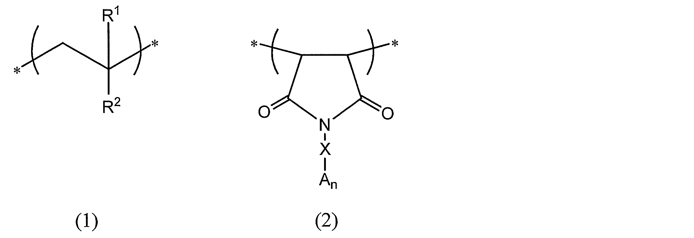
一般式(1)および一般式(2)中、R1は、水素原子またはメチル基を表し、R2は、水素原子、アルキル基、アルコキシ基またはアリール基を表し、Xは、n+1価の連結基を表し、Aは酸性基を表し、nは1~10の整数を表し、*は連結手を表す。
<7> 重合体の酸価が50mgKOH/g以上である<1>~<6>のいずれかに記載の感光性樹脂組成物。
<8> 重合体は、20℃/分で昇温したときの300℃における重量減少率が5%以下である、<1>~<7>のいずれかに記載の感光性樹脂組成物。
<9> さらにフィラーを含む、<1>~<8>のいずれかに記載の感光性樹脂組成物。
<10> さらに密着性付与剤を含む、<1>~<9>のいずれかに記載の感光性樹脂組成物。
<11> アンダーフィル用である、<1>~<10>のいずれかに記載の感光性樹脂組成物。
<12> 液状である、<1>~<11>のいずれかに記載の感光性樹脂組成物。
<13> シート状である、<1>~<11>のいずれかに記載の感光性樹脂組成物。
<14> 半導体ウエハの表面に、<1>~<13>のいずれかに記載の感光性樹脂組成物からなる層を有する積層体。
<15> 半導体ウエハの表面に、<1>~<13>のいずれかに記載の感光性樹脂組成物を硬化してなる硬化物層を有する積層体。
<16> <12>に記載の感光性樹脂組成物を半導体ウエハに適用する工程と、
半導体ウエハに適用された感光性樹脂組成物を乾燥させる工程と、
乾燥された感光性樹脂組成物を露光する工程と、
露光された感光性樹脂組成物を現像する工程と、
現像された感光性樹脂組成物の表面に、被着体を加熱圧着する工程と、
を含む半導体デバイスの製造方法。
<17> <13>に記載の感光性樹脂組成物を半導体ウエハに積層する工程と、
半導体ウエハに積層された感光性樹脂組成物を露光する工程と、
露光された感光性樹脂組成物を現像する工程と、
現像された感光性樹脂組成物の表面に、被着体を加熱圧着する工程と、
を含む半導体デバイスの製造方法。
<18> <16>または<17>に記載の方法で製造された半導体デバイス。
<1> 酸基含有マレイミドに由来する繰り返し単位を含む重合体と、架橋剤と、光重合開始剤と、熱重合開始剤とを含む感光性樹脂組成物。
<2> 重合体が、さらに、ビニル化合物に由来する繰り返し単位を含む、<1>に記載の感光性樹脂組成物。
<3> さらに溶剤を含む、<1>または<2>に記載の感光性樹脂組成物。
<4> 架橋剤が、エチレン性不飽和結合を有する基を2個以上有する化合物である、<1>~<3>のいずれかに記載の感光性樹脂組成物。
<5> 架橋剤が、下記式で表される部分構造を有する、<1>~<4>のいずれかに記載の感光性樹脂組成物;ただし、式中の*は連結手である。
<7> 重合体の酸価が50mgKOH/g以上である<1>~<6>のいずれかに記載の感光性樹脂組成物。
<8> 重合体は、20℃/分で昇温したときの300℃における重量減少率が5%以下である、<1>~<7>のいずれかに記載の感光性樹脂組成物。
<9> さらにフィラーを含む、<1>~<8>のいずれかに記載の感光性樹脂組成物。
<10> さらに密着性付与剤を含む、<1>~<9>のいずれかに記載の感光性樹脂組成物。
<11> アンダーフィル用である、<1>~<10>のいずれかに記載の感光性樹脂組成物。
<12> 液状である、<1>~<11>のいずれかに記載の感光性樹脂組成物。
<13> シート状である、<1>~<11>のいずれかに記載の感光性樹脂組成物。
<14> 半導体ウエハの表面に、<1>~<13>のいずれかに記載の感光性樹脂組成物からなる層を有する積層体。
<15> 半導体ウエハの表面に、<1>~<13>のいずれかに記載の感光性樹脂組成物を硬化してなる硬化物層を有する積層体。
<16> <12>に記載の感光性樹脂組成物を半導体ウエハに適用する工程と、
半導体ウエハに適用された感光性樹脂組成物を乾燥させる工程と、
乾燥された感光性樹脂組成物を露光する工程と、
露光された感光性樹脂組成物を現像する工程と、
現像された感光性樹脂組成物の表面に、被着体を加熱圧着する工程と、
を含む半導体デバイスの製造方法。
<17> <13>に記載の感光性樹脂組成物を半導体ウエハに積層する工程と、
半導体ウエハに積層された感光性樹脂組成物を露光する工程と、
露光された感光性樹脂組成物を現像する工程と、
現像された感光性樹脂組成物の表面に、被着体を加熱圧着する工程と、
を含む半導体デバイスの製造方法。
<18> <16>または<17>に記載の方法で製造された半導体デバイス。
耐熱性、現像性および硬化性に優れた感光性樹脂組成物、かかる感光性樹脂組成物を用いた硬化膜、硬化膜の製造方法および半導体デバイスを提供可能となった。
以下に記載する本発明における構成要素の説明は、本発明の代表的な実施態様に基づいてなされることがあるが、本発明はそのような実施態様に限定されるものではない。
本明細書における基(原子団)の表記に於いて、置換および無置換を記していない表記は、置換基を有さないものと共に置換基を有するものをも包含するものである。例えば、「アルキル基」とは、置換基を有さないアルキル基(無置換アルキル基)のみならず、置換基を有するアルキル基(置換アルキル基)をも包含するものである。
本明細書中における「活性光線」とは、例えば、水銀灯の輝線スペクトル、エキシマレーザーに代表される遠紫外線、極紫外線(EUV光)、X線、電子線等を意味する。また、本発明において光とは、活性光線または放射線を意味する。本明細書中における「露光」とは、特に断らない限り、水銀灯、エキシマレーザーに代表される遠紫外線、X線、EUV光などによる露光のみならず、電子線、イオンビーム等の粒子線による描画も露光に含める。
本明細書において「~」を用いて表される数値範囲は、「~」の前後に記載される数値を下限値および上限値として含む範囲を意味する。
本明細書において、“(メタ)アクリレート”はアクリレートおよびメタクリレートの双方、または、いずれかを表し、“(メタ)アクリル”はアクリルおよびメタクリルの双方、または、いずれかを表し、“(メタ)アクリロイル”はアクリロイルおよびメタクリロイルの双方、または、いずれかを表す。
本明細書において「工程」との語は、独立した工程だけではなく、他の工程と明確に区別できない場合であってもその工程の所期の作用が達成されれば、本用語に含まれる。
本明細書において固形分濃度とは、組成物の総重量に対する、溶剤を除く他の成分の重量の重量百分率である。また、固形分濃度は、特に述べない限り25℃における濃度をいう。
本明細書において、重量平均分子量は、GPC測定によるポリスチレン換算値として定義される。本明細書において、重量平均分子量(Mw)および数平均分子量(Mn)は、例えば、HLC-8220(東ソー(株)製)を用い、カラムとしてTSKgel Super AWM―H(東ソー(株)製、6.0mmID×15.0cmを用いることによって求めることができる。溶離液は特に述べない限り、10mmol/L リチウムブロミドNMP(N-メチルピロリジノン)溶液を用いて測定したものとする。
<感光性樹脂組成物>
本発明の感光性樹脂組成物は、酸基含有マレイミドに由来する繰り返し単位を含む重合体と、架橋剤と、光重合開始剤と、熱重合開始剤とを含むことを特徴とする。
本発明の感光性樹脂組成物は、酸基含有マレイミドに由来する繰り返し単位を含む重合体を含むので、耐熱性に優れた硬化物を形成できる。また、マレイミドは酸基を含有しているので、現像性に優れたパターンを形成することができる。特に、マレイミドと酸基を同じ繰り返し単位に含む重合体とすることによって、耐熱性が向上する。また、光重合開始剤と熱重合開始剤とを含むので、重合性化合物の重合反応が効率よく進行し、硬化性に優れる。
以下本発明を詳細に説明する。
本発明の感光性樹脂組成物は、酸基含有マレイミドに由来する繰り返し単位を含む重合体と、架橋剤と、光重合開始剤と、熱重合開始剤とを含むことを特徴とする。
本発明の感光性樹脂組成物は、酸基含有マレイミドに由来する繰り返し単位を含む重合体を含むので、耐熱性に優れた硬化物を形成できる。また、マレイミドは酸基を含有しているので、現像性に優れたパターンを形成することができる。特に、マレイミドと酸基を同じ繰り返し単位に含む重合体とすることによって、耐熱性が向上する。また、光重合開始剤と熱重合開始剤とを含むので、重合性化合物の重合反応が効率よく進行し、硬化性に優れる。
以下本発明を詳細に説明する。
<<酸基含有マレイミドに由来する繰り返し単位を含む重合体>>
本発明の感光性樹脂組成物は、酸基含有マレイミドに由来する繰り返し単位を含む重合体(以下、マレイミド系重合体ともいう)を含有する。
本発明において用いられるマレイミド系重合体は、更に、ビニル化合物に由来する繰り返し単位を含有することが好ましい。なかでも、下記一般式(1)で表される繰り返し単位と、下記一般式(2)で表される繰り返し単位とを含む重合体が好ましい。
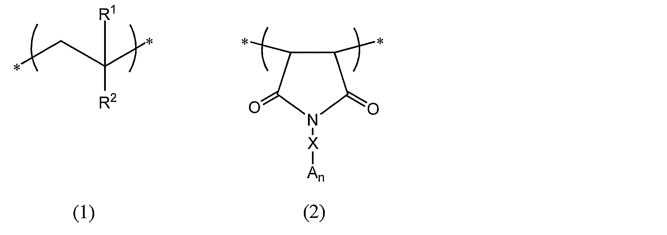
一般式(1)および一般式(2)中、R1は、水素原子またはメチル基を表し、R2は、水素原子、アルキル基、アルコキシ基またはアリール基を表し、Xは、n+1価の連結基を表し、Aは酸性基を表し、nは1~10の整数を表し、*は連結手を表す。
本発明の感光性樹脂組成物は、酸基含有マレイミドに由来する繰り返し単位を含む重合体(以下、マレイミド系重合体ともいう)を含有する。
本発明において用いられるマレイミド系重合体は、更に、ビニル化合物に由来する繰り返し単位を含有することが好ましい。なかでも、下記一般式(1)で表される繰り返し単位と、下記一般式(2)で表される繰り返し単位とを含む重合体が好ましい。
一般式(1)において、R1は、水素原子またはメチル基を表し、水素原子が好ましい。
一般式(1)において、R2は、水素原子、アルキル基、アルコキシ基またはアリール基を表す。
アルキル基としては、炭素数1~30のアルキル基が好ましく、炭素数1~20のアルキル基が好ましい。アルキル基は、直鎖、分岐、環状のいずれでもよい。
アルコキシ基としては、炭素数1~30のアルコキシ基が好ましく、炭素数1~20のアルコキシ基が好ましい。アルコキシ基は、直鎖、分岐、環状のいずれでもよい。
アリール基は、炭素数6~30のアリール基が好ましく、炭素数6~20のアリール基がより好ましく、フェニル基が特に好ましい。
一般式(1)のR2は、水素原子またはフェニル基が好ましく、フェニル基が特に好ましい。R2を水素原子またはフェニル基とすることにより、耐熱性をより向上できる。特にフェニル基とすることにより耐熱性を特に向上できる。
一般式(1)において、R2は、水素原子、アルキル基、アルコキシ基またはアリール基を表す。
アルキル基としては、炭素数1~30のアルキル基が好ましく、炭素数1~20のアルキル基が好ましい。アルキル基は、直鎖、分岐、環状のいずれでもよい。
アルコキシ基としては、炭素数1~30のアルコキシ基が好ましく、炭素数1~20のアルコキシ基が好ましい。アルコキシ基は、直鎖、分岐、環状のいずれでもよい。
アリール基は、炭素数6~30のアリール基が好ましく、炭素数6~20のアリール基がより好ましく、フェニル基が特に好ましい。
一般式(1)のR2は、水素原子またはフェニル基が好ましく、フェニル基が特に好ましい。R2を水素原子またはフェニル基とすることにより、耐熱性をより向上できる。特にフェニル基とすることにより耐熱性を特に向上できる。
一般式(2)において、Xは、n+1価の連結基を表す。n+1価の連結基としては、脂肪族炭化水素基、芳香族炭化水素基、-O-、-NR’-(R’は、水素原子、置換基を有していてもよいアルキル基または置換基を有していてもよいアリール基を表し、水素原子が好ましい)で表される構造、-SO2-、-CO-、-O-および-S-から選ばれる少なくとも一つを含む基が挙げられる。なかでも、耐熱性の観点から、芳香族炭化水素基が好ましい。
例えば、2価の連結基としては、アルキレン基、アリーレン基、-O-、-NR’-(R’は、水素原子、置換基を有していてもよいアルキル基または置換基を有していてもよいアリール基を表し、水素原子が好ましい)で表される構造、-SO2-、-CO-、-O-および-S-から選ばれる少なくとも一つを含む基が挙げられる。
アルキレン基としては、炭素数2~20のアルキレン基が好ましく、炭素数2~10のアルキレン基がより好ましい。
アリーレン基としては、炭素数6~30のアリーレン基が好ましく、炭素数6~20のアリーレン基がより好ましい。
2価の連結基としては、フェニレン基が特に好ましい。
3価の連結基の例としては、2価の連結基の例として挙げた基のうち、1つの水素原子を取り除いた基が挙げられる。例えば、3置換のベンゼン環などが挙げられる。
例えば、2価の連結基としては、アルキレン基、アリーレン基、-O-、-NR’-(R’は、水素原子、置換基を有していてもよいアルキル基または置換基を有していてもよいアリール基を表し、水素原子が好ましい)で表される構造、-SO2-、-CO-、-O-および-S-から選ばれる少なくとも一つを含む基が挙げられる。
アルキレン基としては、炭素数2~20のアルキレン基が好ましく、炭素数2~10のアルキレン基がより好ましい。
アリーレン基としては、炭素数6~30のアリーレン基が好ましく、炭素数6~20のアリーレン基がより好ましい。
2価の連結基としては、フェニレン基が特に好ましい。
3価の連結基の例としては、2価の連結基の例として挙げた基のうち、1つの水素原子を取り除いた基が挙げられる。例えば、3置換のベンゼン環などが挙げられる。
一般式(2)において、Aは酸性基を表し、アルカリ現像性の観点から、カルボキシル基、ホスホン酸基、リン酸基、スルホン酸基、水酸基、スルホンアミド基が好ましく、現像性の観点から、スルホンアミド基またはカルボキシル基がより好ましく、カルボキシル基が特に好ましい。
nは1~10の整数を表し、1~5が好ましく、1~2がさらに好ましい。
本発明において用いられるマレイミド系重合体において、一般式(1)で表される繰り返し単位と、一般式(2)で表される繰り返し単位との比率は、モル比で、1:1~6:1が好ましく、1:1~4:1がより好ましく、1:1~3:1がさらに好ましい。
本発明において用いられるマレイミド系重合体は、一般式(1)で表される繰り返し単位および一般式(2)で表される繰り返し単位以外の繰り返し単位(以下、他の繰り返し単位ともいう)を含んでいてもよい。
他の繰り返し単位としては、例えば、不飽和カルボン酸(例えば、アクリル酸、メタクリル酸、イタコン酸、クロトン酸、イソクロトン酸、マレイン酸等)、不飽和カルボン酸とアルコール化合物とのエステル、不飽和カルボン酸とアミン化合物とのアミド、不飽和カルボン酸無水物等に由来する繰り返し単位が挙げられる。
全繰り返し単位中における、他の繰り返し単位の含有量は、10モル%以下が好ましく、5モル%以下がより好ましく、実質的に含有しないことが特に好ましい。実質的に含有しないとは、例えば、全繰り返し単位中における、他の繰り返し単位の含有量が1モル%以下であることが好ましく、0.5モル%以下であることがより好ましく、含有しないことが特に好ましい。
他の繰り返し単位としては、例えば、不飽和カルボン酸(例えば、アクリル酸、メタクリル酸、イタコン酸、クロトン酸、イソクロトン酸、マレイン酸等)、不飽和カルボン酸とアルコール化合物とのエステル、不飽和カルボン酸とアミン化合物とのアミド、不飽和カルボン酸無水物等に由来する繰り返し単位が挙げられる。
全繰り返し単位中における、他の繰り返し単位の含有量は、10モル%以下が好ましく、5モル%以下がより好ましく、実質的に含有しないことが特に好ましい。実質的に含有しないとは、例えば、全繰り返し単位中における、他の繰り返し単位の含有量が1モル%以下であることが好ましく、0.5モル%以下であることがより好ましく、含有しないことが特に好ましい。
以下に、一般式(1)で表される繰り返し単位と、下記一般式(2)で表される繰り返し単位とを含むマレイミド系重合体の具体例を記載するが、本発明はこれらに限定されるものではない。これらは、それぞれ単独でまたは2種以上を混合して用いることができる。なお、以下の式中におけるMeは、メチル基を表す。
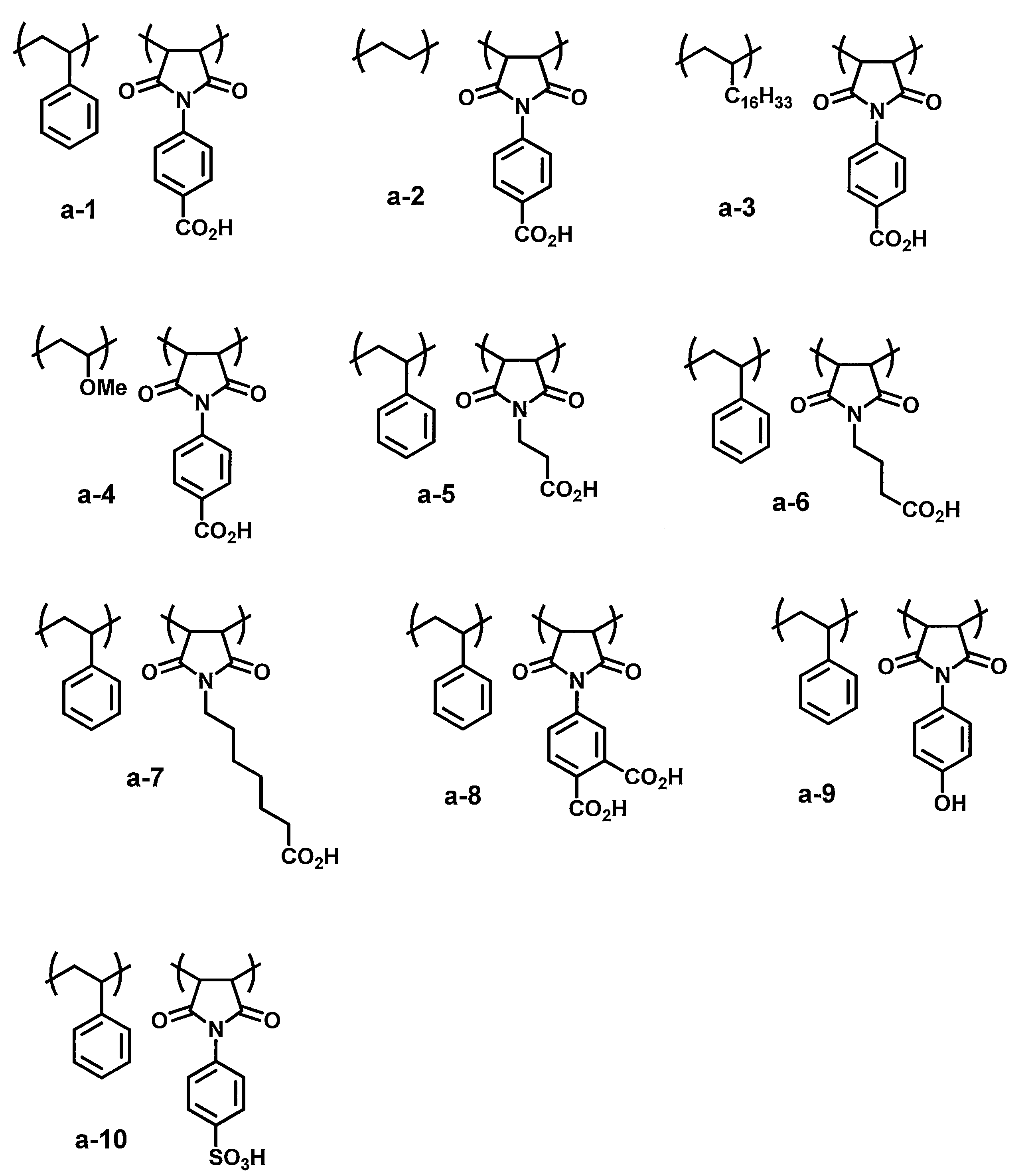
上述した一般式(1)で表される繰り返し単位と、一般式(2)で表される繰り返し単位とを含む重合体は、ビニル化合物と酸性基含有マレイミドを共重合して合成できる。
例えば、例えばビニル化合物と酸性基含有マレイミドをラジカル共重合させて得ることが出来る。すなわち、有機溶媒中、ビニル化合物と酸性基含有マレイミドを任意の割合で混合し、さらに、必要に応じてラジカル重合開始剤や連鎖移動剤などを添加して反応させて合成できる。
また、酸性基含有マレイミドは、例えば、無水マレイン酸と酸性基含有アミン化合物を用いてイミド化することで得ることが出来る。
別の合成法として、ビニル化合物と無水マレイン酸をラジカル共重合させた後、さらにアミン化合物を用いてイミド化することで得ることも出来る。このとき、必要に応じて塩基や酸、酸無水物などを添加して合成することも出来る。
例えば、例えばビニル化合物と酸性基含有マレイミドをラジカル共重合させて得ることが出来る。すなわち、有機溶媒中、ビニル化合物と酸性基含有マレイミドを任意の割合で混合し、さらに、必要に応じてラジカル重合開始剤や連鎖移動剤などを添加して反応させて合成できる。
また、酸性基含有マレイミドは、例えば、無水マレイン酸と酸性基含有アミン化合物を用いてイミド化することで得ることが出来る。
別の合成法として、ビニル化合物と無水マレイン酸をラジカル共重合させた後、さらにアミン化合物を用いてイミド化することで得ることも出来る。このとき、必要に応じて塩基や酸、酸無水物などを添加して合成することも出来る。
ビニル化合物としては、エチレン性不飽和結合を有する基を持つ化合物であれば特に制限されないが、例えば、α-オレフィン化合物、共役ジエン化合物、芳香族ビニル化合物、ビニルエーテル化合物、ビニルエステル化合物、(メタ)アクリレート化合物、(メタ)アクリルアミド化合物などが好ましく用いられる。中でも、共重合体の耐熱性の観点から、α-オレフィン化合物、芳香族ビニル化合物が好ましく、さらに芳香族ビニル化合物がより好ましく用いられる。
α-オレフィンとしては、炭素数2~30のα-オレフィンが好ましく、例えば、エチレン、プロピレン、1-ブテン、1-ヘキセン、1-オクテン、1-デセン、1-ドデセン、1-オクタデセンなどが挙げられる。中でもエチレンが好ましく用いられる。
芳香族ビニル化合物としては、スチレン、アルキルスチレン、アリールスチレン、ハロゲン化スチレン、アルコキシスチレン、ビニル安息香酸エステル等を挙げられる。中でもスチレンが好ましく用いられる。
アルキルスチレンの具体例としては、o-メチルスチレン、m-メチルスチレン、p-メチルスチレン、o-エチルスチレン、m-エチルスチレン、p-エチルスチレン、o-n-プロピルスチレン、m-n-プロピルスチレン、p-n-プロピルスチレン、o-イソプロピルスチレン、m-イソプロピルスチレン、p-イソプロピルスチレン、m-n-ブチルスチレン、p-n-ブチルスチレン、p-tert-ブチルスチレン、4-ブテニルスチレン、2,4-ジメチルスチレン、2,5-ジメチルスチレン、3,5-ジメチルスチレン、メシチルスチレン等が挙げられる。
アリールスチレンの具体例としては、p-フェニルスチレン等が挙げられる。
ハロゲン化スチレンの具体例としては、o-フルオロスチレン、m-フルオロスチレン、p-フルオロスチレン、o-クロロスチレン、m-クロロスチレン、p-クロロスチレン、o-ブロモスチレン、m-ブロモスチレン、p-ブロモスチレン、o-メチル-p-フルオロスチレン等が挙げられる。
アルコキシスチレンの具体例としては、o-メトキシスチレン、m-メトキシスチレン、p-メトキシスチレン等が挙げられる。
α-オレフィンとしては、炭素数2~30のα-オレフィンが好ましく、例えば、エチレン、プロピレン、1-ブテン、1-ヘキセン、1-オクテン、1-デセン、1-ドデセン、1-オクタデセンなどが挙げられる。中でもエチレンが好ましく用いられる。
芳香族ビニル化合物としては、スチレン、アルキルスチレン、アリールスチレン、ハロゲン化スチレン、アルコキシスチレン、ビニル安息香酸エステル等を挙げられる。中でもスチレンが好ましく用いられる。
アルキルスチレンの具体例としては、o-メチルスチレン、m-メチルスチレン、p-メチルスチレン、o-エチルスチレン、m-エチルスチレン、p-エチルスチレン、o-n-プロピルスチレン、m-n-プロピルスチレン、p-n-プロピルスチレン、o-イソプロピルスチレン、m-イソプロピルスチレン、p-イソプロピルスチレン、m-n-ブチルスチレン、p-n-ブチルスチレン、p-tert-ブチルスチレン、4-ブテニルスチレン、2,4-ジメチルスチレン、2,5-ジメチルスチレン、3,5-ジメチルスチレン、メシチルスチレン等が挙げられる。
アリールスチレンの具体例としては、p-フェニルスチレン等が挙げられる。
ハロゲン化スチレンの具体例としては、o-フルオロスチレン、m-フルオロスチレン、p-フルオロスチレン、o-クロロスチレン、m-クロロスチレン、p-クロロスチレン、o-ブロモスチレン、m-ブロモスチレン、p-ブロモスチレン、o-メチル-p-フルオロスチレン等が挙げられる。
アルコキシスチレンの具体例としては、o-メトキシスチレン、m-メトキシスチレン、p-メトキシスチレン等が挙げられる。
酸性基含有マレイミドとしては、一般式(2a)で表される構造を有する化合物を用いることが出来る。
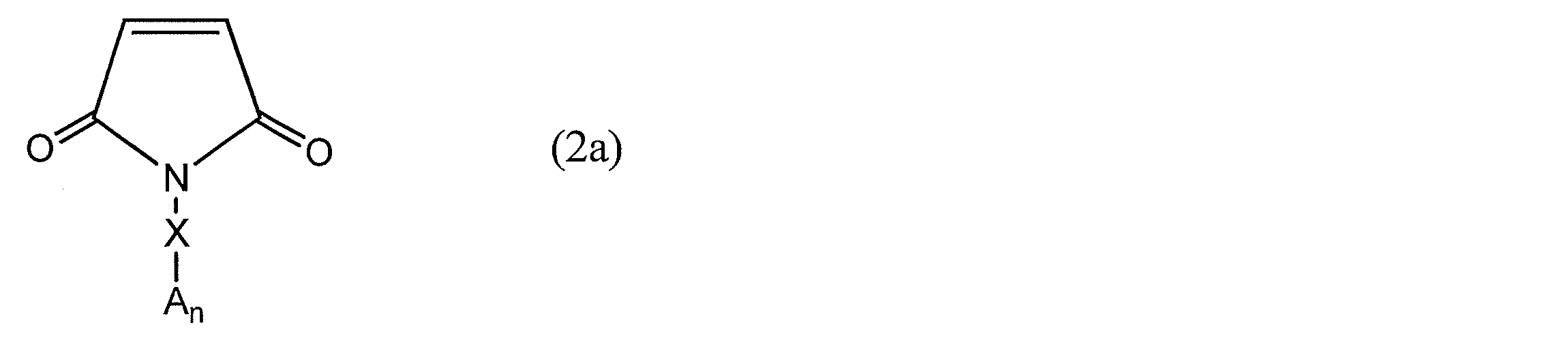
一般式(2a)のX、Aおよびnは、一般式(2)のX、Aおよびnと同義であり、好ましい範囲も同様である。
マレイミド系重合体の酸価は、現像性の観点から50mgKOH/g以上であることが好ましく、80~300mgKOH/gであることがより好ましく、100~250mgKOH/gであることが特に好ましい。このような範囲とすることにより、本発明の効果がより効果的に発揮される。
マレイミド系重合体の、20℃/分で昇温したときの300℃における重量減少率は、5%以下であることが好ましく、3%以下であることがより好ましく、1%以下であることが特に好ましい。このような範囲とすることにより、耐熱性がより向上する。
マレイミド系重合体の重量平均分子量は、ゲルパーミエーションクロマトグラフィー(GPC)法によるポリスチレン換算で、2000~1000000が好ましく、3000~500000がより好ましく、5000~100000がさらに好ましい。2000以上であれば、耐熱性がより良好となり、1000000以下であれば現像性がより良好となる。
本発明の感光性樹脂組成物は、マレイミド系重合体を、感光性樹脂組成物の全固形分に対し、30~90質量%含有することが好ましく、40~90質量%含有することがより好ましく、50~90質量%含有することが特に好ましい。
<架橋剤>
本発明の感光性樹脂組成物は、架橋剤を含有する。
架橋剤は、2個以上の重合性基を有する化合物であって、活性光線、放射線、光、熱、ラジカルまたは酸の作用により重合可能な公知の化合物を用いることができる。このような化合物は産業分野において広く知られているものであり、本発明においてはこれらを特に限定なく用いることができる。これらは、例えば、モノマー、プレポリマー、オリゴマー又はそれらの混合物並びにそれらの多量体などの化学的形態のいずれであってもよい。
なお、本発明における架橋剤は、上記したマレイミド系重合体とは異なる化合物である。すなわち、本発明の架橋剤は、酸基含有マレイミドに由来する繰り返し単位を含まない化合物である。
本発明の感光性樹脂組成物は、架橋剤を含有する。
架橋剤は、2個以上の重合性基を有する化合物であって、活性光線、放射線、光、熱、ラジカルまたは酸の作用により重合可能な公知の化合物を用いることができる。このような化合物は産業分野において広く知られているものであり、本発明においてはこれらを特に限定なく用いることができる。これらは、例えば、モノマー、プレポリマー、オリゴマー又はそれらの混合物並びにそれらの多量体などの化学的形態のいずれであってもよい。
なお、本発明における架橋剤は、上記したマレイミド系重合体とは異なる化合物である。すなわち、本発明の架橋剤は、酸基含有マレイミドに由来する繰り返し単位を含まない化合物である。
本発明において、モノマータイプの架橋剤(以下、重合性モノマーともいう)は、高分子化合物とは異なる化合物である。重合性モノマーは、典型的には、低分子化合物であり、分子量2000以下の低分子化合物であることが好ましく、1500以下の低分子化合物であることがより好ましく、分子量900以下の低分子化合物であることがさらに好ましい。なお、重合性モノマーの分子量は、通常、100以上である。
重合性基は、例えば、付加重合反応し得る官能基であることが好ましい。付加重合反応し得る官能基としては、エチレン性不飽和結合を有する基、アミノ基、エポキシ基等が挙げられる。また、重合性基は、光照射によりラジカルを発生し得る官能基であってもよく、そのような重合性基としては、例えば、チオール基、ハロゲン基等が挙げられる。なかでも、重合性基は、エチレン性不飽和結合を有する基が好ましい。エチレン性不飽和結合基としては、アクリル基、メタクリル基、アリル基およびスチリル基が好ましい。
すなわち、本発明において、架橋剤は、エチレン性不飽和結合を有する基を有する化合物が好ましい。
すなわち、本発明において、架橋剤は、エチレン性不飽和結合を有する基を有する化合物が好ましい。
架橋剤は、現像性および耐熱性の観点から、重合性基を2個以上含有する2官能以上の架橋剤を少なくとも1種含むことが好ましく、3官能以上の架橋剤を少なくとも1種含むことがより好ましい。なかでも、現像性および耐熱性をより向上できるという理由から、エチレン性不飽和結合を有する基を2個以上有する2官能以上の架橋剤が特に好ましい。
また、本発明の感光性樹脂組成物は、重合性基としてエポキシ基を有する化合物を含有してもよいが、現像性および耐熱性をより向上できるという理由から、架橋剤100質量部中におけるエポキシ基を有する化合物の含有量は、10質量%以下が好ましく、5質量%以下が好ましく、実質的に含有しないことが特に好ましい。なお、実質的に含有しないとは、例えば、エポキシ基を有する化合物の含有量が1質量%以下が好ましく、0.5質量%以下がより好ましく、0.1質量%以下が特に好ましく、含有しないことが特に好ましい。
また、本発明の感光性樹脂組成物は、重合性基としてエポキシ基を有する化合物を含有してもよいが、現像性および耐熱性をより向上できるという理由から、架橋剤100質量部中におけるエポキシ基を有する化合物の含有量は、10質量%以下が好ましく、5質量%以下が好ましく、実質的に含有しないことが特に好ましい。なお、実質的に含有しないとは、例えば、エポキシ基を有する化合物の含有量が1質量%以下が好ましく、0.5質量%以下がより好ましく、0.1質量%以下が特に好ましく、含有しないことが特に好ましい。
架橋剤としては、具体的にはラジカル重合性化合物(B1)、イオン重合性化合物(B2)が挙げられる。
<<ラジカル重合性化合物(B1)>>
ラジカル重合性化合物(B1)としては、炭素数3~35の(メタ)アクリルアミド化合物(B11)、炭素数4~35の(メタ)アクリレート化合物(B12)、炭素数6~35の芳香族ビニル化合物(B13)、炭素数3~20のビニルエーテル化合物(B14)及びその他のラジカル重合性化合物(B15)等が挙げられる。ラジカル重合性化合物(B1)は1種を単独で用いても、2種以上を併用してもよい。また、必要により、ハイドロキノン、メチルエーテルハイドロキノン類等の重合禁止剤を併用してもよい。
<<ラジカル重合性化合物(B1)>>
ラジカル重合性化合物(B1)としては、炭素数3~35の(メタ)アクリルアミド化合物(B11)、炭素数4~35の(メタ)アクリレート化合物(B12)、炭素数6~35の芳香族ビニル化合物(B13)、炭素数3~20のビニルエーテル化合物(B14)及びその他のラジカル重合性化合物(B15)等が挙げられる。ラジカル重合性化合物(B1)は1種を単独で用いても、2種以上を併用してもよい。また、必要により、ハイドロキノン、メチルエーテルハイドロキノン類等の重合禁止剤を併用してもよい。
炭素数4~35の(メタ)アクリレート化合物(B12)としては、例えば以下の二官能~六官能の(メタ)アクリレートが挙げられる。以下において、EOはエチレンオキサイドを表し、POはプロピレンオキサイドを表す。
二官能(メタ)アクリレートとしては、1,4-ブタンジ(メタ)アクリレート、1,6-ヘキサンジアクリレート、ポリプロピレンジアクリレート、1,6-ヘキサンジオールジ(メタ)アクリレート、1,10-デカンジオールジ(メタ)アクリレート、ネオペンチルジアクリレート、ネオペンチルグリコールジ(メタ)アクリレート、2,4-ジメチル-1,5-ペンタンジオールジ(メタ)アクリレート、ブチルエチルプロパンジオール(メタ)アクリレート、エトキシ化シクロヘキサンメタノールジ(メタ)アクリレート、ポリエチレングリコールジ(メタ)アクリレート、オリゴエチレングリコールジ(メタ)アクリレート、エチレングリコールジ(メタ)アクリレート、2-エチル-2-ブチル-ブタンジオールジ(メタ)アクリレート、ヒドロキシピバリン酸ネオペンチルグリコールジ(メタ)アクリレート、EO変性ビスフェノールAジ(メタ)アクリレート、ビスフェノールFポリエトキシジ(メタ)アクリレート、ポリプロピレングリコールジ(メタ)アクリレート、オリゴプロピレングリコールジ(メタ)アクリレート、1,4-ブタンジオールジ(メタ)アクリレート、2-エチル-2-ブチル-プロパンジオールジ(メタ)アクリレート、1,9-ノナンジ(メタ)アクリレート、プロポキシ化エトキシ化ビスフェノールAジ(メタ)アクリレート及びトリシクロデカンジ(メタ)アクリレート等が挙げられる。
三官能の(メタ)アクリレートとしては、トリメチロールプロパントリ(メタ)アクリレート、トリメチロールエタントリ(メタ)アクリレート、トリメチロールプロパンのアルキレンオキサイド変性トリ(メタ)アクリレート、ペンタエリスリトールトリ(メタ)アクリレート、ジペンタエリスルトールトリ(メタ)アクリレート、トリメチロールプロパントリ((メタ)アクリロイルオキシプロピル)エーテル、イソシアヌル酸アルキレンオキサイド変性トリ(メタ)アクリレート、プロピオン酸ジペンタエリスリトールトリ(メタ)アクリレート、トリ((メタ)アクリロイルオキシエチル)イソシアヌレート、ヒドロキシピバルアルデヒド変性ジメチロールプロパントリ(メタ)アクリレート、ソルビトールトリ(メタ)アクリレート、プロポキシ化トリメチロールプロパントリ(メタ)アクリレート及びエトキシ化グリセリントリアクリレート等が挙げられる。
四官能の(メタ)アクリレートとしては、ペンタエリスリトールテトラ(メタ)アクリレート、ソルビトールテトラ(メタ)アクリレート、ジトリメチロールプロパンテトラ(メタ)アクリレート、プロピオン酸ジペンタエリスリトールテトラ(メタ)アクリレート及びエトキシ化ペンタエリスリトールテトラ(メタ)アクリレート等が挙げられる。
五官能の(メタ)アクリレートとしては、ソルビトールペンタ(メタ)アクリレート及びジペンタエリスリトールペンタ(メタ)アクリレートが挙げられる。
六官能の(メタ)アクリレートとしては、ジペンタエリスリトールヘキサ(メタ)アクリレート、ソルビトールヘキサ(メタ)アクリレート、フォスファゼンのアルキレンオキサイド変性ヘキサ(メタ)アクリレート及びカプロラクトン変性ジペンタエリスリトールヘキサ(メタ)アクリレート等が挙げられる。
炭素数3~35のビニルエーテル化合物(B14)としては、例えば以下の多官能ビニルエーテルが挙げられる。
多官能ビニルエーテルとしては、例えば、エチレングリコールジビニルエーテル、ジエチレングリコールジビニルエーテル、ポリエチレングリコールジビニルエーテル、プロピレングリコールジビニルエーテル、ブチレングリコールジビニルエーテル、ヘキサンジオールジビニルエーテル、ビスフェノールAアルキレンオキサイドジビニルエーテル、ビスフェノールFアルキレンオキサイドジビニルエーテル等のジビニルエーテル類;トリメチロールエタントリビニルエーテル、トリメチロールプロパントリビニルエーテル、ジトリメチロールプロパンテトラビニルエーテル、グリセリントリビニルエーテル、ペンタエリスリトールテトラビニルエーテル、ジペンタエリスリトールペンタビニルエーテル、ジペンタエリスリトールヘキサビニルエーテル、エチレンオキサイド付加トリメチロールプロパントリビニルエーテル、プロピレンオキサイド付加トリメチロールプロパントリビニルエーテル、エチレンオキサイド付加ジトリメチロールプロパンテトラビニルエーテル、プロピレンオキサイド付加ジトリメチロールプロパンテトラビニルエーテル、エチレンオキサイド付加ペンタエリスリトールテトラビニルエーテル、プロピレンオキサイド付加ペンタエリスリトールテトラビニルエーテル、エチレンオキサイド付加ジペンタエリスリトールヘキサビニルエーテル及びプロピレンオキサイド付加ジペンタエリスリトールヘキサビニルエーテルが挙げられる。
その他のラジカル重合性化合物(B15)としては、ビニルエステル化合物(酢酸ビニル、プロピオン酸ビニル及びバーサチック酸ビニル等)、アリルエステル化合物(酢酸アリル等)、ハロゲン含有単量体(塩化ビニリデン及び塩化ビニル等)及びオレフィン化合物(エチレン及びプロピレン等)等が挙げられる。
これらの内、重合速度の観点から(メタ)アクリルアミド化合物(B11)及び(メタ)アクリレート化合物(B12)が好ましく、特に(メタ)アクリレート化合物(B12)が好ましい。
<<イオン重合性化合物(B2)>>
イオン重合性化合物(B2)としては、炭素数3~20のエポキシ化合物(B21)、炭素数4~20のオキセタン化合物(B22)等が挙げられる。
イオン重合性化合物(B2)としては、炭素数3~20のエポキシ化合物(B21)、炭素数4~20のオキセタン化合物(B22)等が挙げられる。
炭素数3~20のエポキシ化合物(B21)としては、例えば以下の多官能エポキシ化合物が挙げられる。
多官能エポキシ化合物としては、例えば、ビスフェノールAジグリシジルエーテル、ビスフェノールFジグリシジルエーテル、ビスフェノールSジグリシジルエーテル、臭素化ビスフェノールAジグリシジルエーテル、臭素化ビスフェノールFジグリシジルエーテル、臭素化ビスフェノールSジグリシジルエーテル、エポキシノボラック樹脂、水添ビスフェノールAジグリシジルエーテル、水添ビスフェノールFジグリシジルエーテル、水添ビスフェノールSジグリシジルエーテル、3,4-エポキシシクロヘキシルメチル-3’,4’-エポキシシクロヘキサンカルボキシレート、2-(3,4-エポキシシクロヘキシル-5,5-スピロ-3,4-エポキシ)シクロヘキサン-メタ-ジオキサン、ビス(3,4-エポキシシクロヘキシルメチル)アジペート、ビニルシクロヘキセンオキサイド、4-ビニルエポキシシクロヘキサン、ビス(3,4-エポキシ-6-メチルシクロヘキシルメチル)アジペート、3,4-エポキシ-6-メチルシクロヘキシル-3’,4’-エポキシ-6’-メチルシクロヘキサンカルボキシレート、メチレンビス(3,4-エポキシシクロヘキサン)、ジシクロペンタジエンジエポキサイド、エチレングリコールジ(3,4-エポキシシクロヘキシルメチル)エーテル、エチレンビス(3,4-エポキシシクロヘキサンカルボキシレート)、エポキシヘキサヒドロフタル酸ジオクチル、エポキシヘキサヒドロフタル酸ジ-2-エチルヘキシル、1,4-ブタンジオールジグリシジルエーテル、1,6-ヘキサンジオールジグリシジルエーテル、グリセリントリグリシジルエーテル、トリメチロールプロパントリグリシジルエーテル、ポリエチレングリコールジグリシジルエーテル、ポリプロピレングリコールジグリシジルエーテル類、1,1,3-テトラデカジエンジオキサイド、リモネンジオキサイド、1,2,7,8-ジエポキシオクタン及び1,2,5,6-ジエポキシシクロオクタンが挙げられる。
これらのエポキシ化合物の中でも、重合速度に優れるという観点から、芳香族エポキシド及び脂環式エポキシドが好ましく、脂環式エポキシドが特に好ましい。
炭素数4~20のオキセタン化合物(B22)としては、オキセタン環を2個~6個有する化合物等が挙げられる。
オキセタン環を2~6個有する化合物としては、例えば、3,7-ビス(3-オキセタニル)-5-オキサ-ノナン、3,3’-(1,3-(2-メチレニル)プロパンジイルビス(オキシメチレン))ビス-(3-エチルオキセタン)、1,4-ビス[(3-エチル-3-オキセタニルメトキシ)メチル]ベンゼン、1,2-ビス[(3-エチル-3-オキセタニルメトキシ)メチル]エタン、1,3-ビス[(3-エチル-3-オキセタニルメトキシ)メチル]プロパン、エチレングリコールビス(3-エチル-3-オキセタニルメチル)エーテル、ジシクロペンテニルビス(3-エチル-3-オキセタニルメチル)エーテル、トリエチレングリコールビス(3-エチル-3-オキセタニルメチル)エーテル、テトラエチレングリコールビス(3-エチル-3-オキセタニルメチル)エーテル、トリシクロデカンジイルジメチレン(3-エチル-3-オキセタニルメチル)エーテル、トリメチロールプロパントリス(3-エチル-3-オキセタニルメチル)エーテル、1,4-ビス(3-エチル-3-オキセタニルメトキシ)ブタン、1,6-ビス(3-エチル-3-オキセタニルメトキシ)ヘキサン、ペンタエリスリトールトリス(3-エチル-3-オキセタニルメチル)エーテル、ペンタエリスリトールテトラキス(3-エチル-3-オキセタニルメチル)エーテル、ポリエチレングリコールビス(3-エチル-3-オキセタニルメチル)エーテル、ジペンタエリスリトールヘキサキス(3-エチル-3-オキセタニルメチル)エーテル、ジペンタエリスリトールペンタキス(3-エチル-3-オキセタニルメチル)エーテル、ジペンタエリスリトールテトラキス(3-エチル-3-オキセタニルメチル)エーテル、カプロラクトン変性ジペンタエリスリトールヘキサキス(3-エチル-3-オキセタニルメチル)エーテル、カプロラクトン変性ジペンタエリスリトールペンタキス(3-エチル-3-オキセタニルメチル)エーテル、ジトリメチロールプロパンテトラキス(3-エチル-3-オキセタニルメチル)エーテル、EO変性ビスフェノールAビス(3-エチル-3-オキセタニルメチル)エーテル、PO変性ビスフェノールAビス(3-エチル-3-オキセタニルメチル)エーテル、EO変性水添ビスフェノールAビス(3-エチル-3-オキセタニルメチル)エーテル、PO変性水添ビスフェノールAビス(3-エチル-3-オキセタニルメチル)エーテル及びEO変性ビスフェノールF(3-エチル-3-オキセタニルメチル)エーテルが挙げられる。
架橋剤は、エポキシ基、アクリル基、メタクリル基、アリル基およびスチリル基から選ばれる1種以上の重合性基を2個以上有する化合物が好ましく、アクリル基、メタクリル基、アリル基およびスチリル基から選ばれる1種以上の重合性基を2個以上有する化合物がより好ましく、アクリル基、メタクリル基、アリル基およびスチリル基から選ばれる1種以上の重合性基を2個以上有し、かつ、下記部分構造を有する化合物がさらに好ましい。架橋剤が下記部分構造を有することにより、耐熱性をより向上できる。

架橋剤の市販品としては、例えば、A-9300、A-TMPT、A-TMMT、AD-TMP、A-DPH、A-BPE-4、4G(新中村化学工業製、(メタ)アクリレート化合物)などが挙げられる。
本発明の感光性樹脂組成物における架橋剤の含有量は、良好な現像性、接着強度、耐熱性の観点から、感光性樹脂組成物の全固形分に対して、5~75質量%が好ましく、10~70質量%がより好ましく、10~60質量%が更に好ましい。
また、架橋剤と上述したマレイミド系重合体との比率(質量比)は、(架橋剤/マレイミド系重合体)=90/10~10/90であることが好ましく、20/80~80/20であることがより好ましい。
架橋剤は、1種のみであってもよく、2種以上を併用してもよい。2種以上を併用する場合は、合計が上記含有量であることが好ましい。
また、架橋剤と上述したマレイミド系重合体との比率(質量比)は、(架橋剤/マレイミド系重合体)=90/10~10/90であることが好ましく、20/80~80/20であることがより好ましい。
架橋剤は、1種のみであってもよく、2種以上を併用してもよい。2種以上を併用する場合は、合計が上記含有量であることが好ましい。
<単官能重合性化合物>
本発明の感光性樹脂組成物は、重合性基を1個有する単官能重合性化合物を含有してもよい。重合性基としては、上述した架橋剤で説明した範囲と同義であり、好ましい範囲も同様である。
単官能重合性化合物としては、単官能(メタ)アクリレート、単官能(メタ)アクリルアミド、芳香族ビニル化合物、単官能ビニルエーテル、オキセタン環を1個有する化合物などが挙げられる。
本発明の感光性樹脂組成物は、重合性基を1個有する単官能重合性化合物を含有してもよい。重合性基としては、上述した架橋剤で説明した範囲と同義であり、好ましい範囲も同様である。
単官能重合性化合物としては、単官能(メタ)アクリレート、単官能(メタ)アクリルアミド、芳香族ビニル化合物、単官能ビニルエーテル、オキセタン環を1個有する化合物などが挙げられる。
単官能(メタ)アクリレートとしては、エチル(メタ)アクリレート、ヘキシル(メタ)アクリレート、2-エチルヘキシル(メタ)アクリレート、tert-オクチル(メタ)アクリレート、イソアミル(メタ)アクリレート、デシル(メタ)アクリレート、イソデシル(メタ)アクリレート、ステアリル(メタ)アクリレート、イソステアリル(メタ)アクリレート、シクロヘキシル(メタ)アクリレート、4-n-ブチルシクロへキシル(メタ)アクリレート、ボルニル(メタ)アクリレート、イソボルニル(メタ)アクリレート、ベンジル(メタ)アクリレート、2-エチルヘキシルジグリコール(メタ)アクリレート、ブトキシエチル(メタ)アクリレート、2-クロロエチル(メタ)アクリレート、4-ブロモブチル(メタ)アクリレート、シアノエチル(メタ)アクリレート、ベンジル(メタ)アクリレート、ブトキシメチル(メタ)アクリレート、メトキシプロピレンモノアクリレート、3-メトキシブチル(メタ)アクリレート、アルコキシメチル(メタ)アクリレート、2-エチルへキシルカルビトール(メタ)アクリレート、アルコキシエチル(メタ)アクリレート、2-(2-メトキシエトキシ)エチル(メタ)アクリレート、2-(2-ブトキシエトキシ)エチル(メタ)アクリレート、2,2,2-テトラフルオロエチル(メタ)アクリレート、1H,1H,2H,2H-パーフルオロデシル(メタ)アクリレート、4-ブチルフェニル(メタ)アクリレート、フェニル(メタ)アクリレート、2,4,5-テトラメチルフェニル(メタ)アクリレート、4-クロロフェニル(メタ)アクリレート、フェノキシメチル(メタ)アクリレート、フェノキシエチル(メタ)アクリレート、グリシジル(メタ)アクリレート、グリシジロキシブチル(メタ)アクリレート、グリシジロキシエチル(メタ)アクリレート、グリシジロキシプロピル(メタ)アクリレート、ジエチレングリコールモノビニルエーテルモノアクリレート、テトラヒドロフルフリル(メタ)アクリレート、ヒドロキシアルキル(メタ)アクリレート、2-ヒドロキシエチル(メタ)アクリレート、3-ヒドロキシプロピル(メタ)アクリレート、2-ヒドロキシプロピル(メタ)アクリレート、2-ヒドロキシブチル(メタ)アクリレート、4-ヒドロキシブチル(メタ)アクリレート、ジメチルアミノエチル(メタ)アクリレート、ジエチルアミノエチル(メタ)アクリレート、ジメチルアミノプロピル(メタ)アクリレート、ジエチルアミノプロピル(メタ)アクリレート、トリメトキシシリルプロピル(メタ)アクリレート、トリメトキシシリルプロピル(メタ)アクリレート、トリメチルシリルプロピル(メタ)アクリレート、ポリエチレンオキサイドモノメチルエーテル(メタ)アクリレート、オリゴエチレンオキサイドモノメチルエーテル(メタ)アクリレート、ポリエチレンオキサイド(メタ)アクリレート、オリゴエチレンオキサイド(メタ)アクリレート、オリゴエチレンオキサイドモノアルキルエーテル(メタ)アクリレート、ポリエチレンオキサイドモノアルキルエーテル(メタ)アクリレート、ジプロピレングリコール(メタ)アクリレート、ポリプロピレンオキサイドモノアルキルエーテル(メタ)アクリレート、オリゴプロピレンオキサイドモノアルキルエーテル(メタ)アクリレート、2-メタクリロイロキシエチルコハク酸、2-メタクリロイロキシヘキサヒドロフタル酸、2-メタクリロイロキシエチル-2-ヒドロキシプロピルフタレート、ブトキシジエチレングリコール(メタ)アクリレート、トリフロロエチル(メタ)アクリレート、パーフロロオクチルエチル(メタ)アクリレート、2-ヒドロキシ-3-フェノキシプロピル(メタ)アクリレート、EO変性フェノール(メタ)アクリレート、EO変性クレゾール(メタ)アクリレート、EO変性ノニルフェノール(メタ)アクリレート、PO変性ノニルフェノール(メタ)アクリレート及びEO変性-2-エチルヘキシル(メタ)アクリレート等が挙げられる。
単官能(メタ)アクリルアミド化合物としては、例えば、(メタ)アクリルアミド、N-メチル(メタ)アクリルアミド、N-エチル(メタ)アクリルアミド、N-プロピル(メタ)アクリルアミド、N-n-ブチル(メタ)アクリルアミド、N-t-ブチル(メタ)アクリルアミド、N-ブトキシメチル(メタ)アクリルアミド、N-イソプロピル(メタ)アクリルアミド、N-メチロール(メタ)アクリルアミド、N,N-ジメチル(メタ)アクリルアミド、N,N-ジエチル(メタ)アクリルアミド及び(メタ)アクリロイルモルフォリンが挙げられる。
単官能芳香族ビニル化合物(B13)としては、ビニルチオフェン、ビニルフラン、ビニルピリジン、スチレン、メチルスチレン、トリメチルスチレン、エチルスチレン、イソプロピルスチレン、クロルメチルスチレン、メトキシスチレン、アセトキシスチレン、クロルスチレン、ジクロルスチレン、ブロムスチレン、ビニル安息香酸メチルエステル、3-メチルスチレン、4-メチルスチレン、3-エチルスチレン、4-エチルスチレン、3-プロピルスチレン、4-プロピルスチレン、3-ブチルスチレン、4-ブチルスチレン、3-ヘキシルスチレン、4-ヘキシルスチレン、3-オクチルスチレン、4-オクチルスチレン、3-(2-エチルヘキシル)スチレン、4-(2-エチルヘキシル)スチレン、アリルスチレン、イソプロペニルスチレン、ブテニルスチレン、オクテニルスチレン、4-t-ブトキシカルボニルスチレン、4-メトキシスチレン及び4-t-ブトキシスチレン等が挙げられる。
単官能ビニルエーテルとしては、例えば、メチルビニルエーテル、エチルビニルエーテル、プロピルビニルエーテル、n-ブチルビニルエーテル、t-ブチルビニルエーテル、2-エチルヘキシルビニルエーテル、n-ノニルビニルエーテル、ラウリルビニルエーテル、シクロヘキシルビニルエーテル、シクロヘキシルメチルビニルエーテル、4-メチルシクロヘキシルメチルビニルエーテル、ベンジルビニルエーテル、ジシクロペンテニルビニルエーテル、2-ジシクロペンテノキシエチルビニルエーテル、メトキシエチルビニルエーテル、エトキシエチルビニルエーテル、ブトキシエチルビニルエーテル、メトキシエトキシエチルビニルエーテル、エトキシエトキシエチルビニルエーテル、メトキシポリエチレングリコールビニルエーテル、テトラヒドロフリフリルビニルエーテル、2-ヒドロキシエチルビニルエーテル、2-ヒドロキシプロピルビニルエーテル、4-ヒドロキシブチルビニルエーテル、4-ヒドロキシメチルシクロヘキシルメチルビニルエーテル、ジエチレングリコールモノビニルエーテル、ポリエチレングリコールビニルエーテル、クロルエチルビニルエーテル、クロルブチルビニルエーテル、クロルエトキシエチルビニルエーテル、フェニルエチルビニルエーテル及びフェノキシポリエチレングリコールビニルエーテルが挙げられる。
単官能エポキシ化合物としては、例えば、フェニルグリシジルエーテル、p-tert―ブチルフェニルグリシジルエーテル、ブチルグリシジルエーテル、2-エチルヘキシルグリシジルエーテル、アリルグリシジルエーテル、1,2-ブチレンオキサイド、1,3-ブタジエンモノオキサイド、1,2-エポキシドデカン、エピクロロヒドリン、1,2-エポキシデカン、スチレンオキサイド、シクロヘキセンオキサイド、3-メタクリロイルオキシメチルシクロヘキセンオキサイド、3-アクリロイルオキシメチルシクロヘキセンオキサイド及び3-ビニルシクロヘキセンオキサイドが挙げられる。
オキセタン環を1個有する化合物としては、例えば、3-エチル-3-ヒドロキシメチルオキセタン、3-(メタ)アリルオキシメチル-3-エチルオキセタン、(3-エチル-3-オキセタニルメトキシ)メチルベンゼン、4-フルオロ-[1-(3-エチル-3-オキセタニルメトキシ)メチル]ベンゼン、4-メトキシ-[1-(3-エチル-3-オキセタニルメトキシ)メチル]ベンゼン、[1-(3-エチル-3-オキセタニルメトキシ)エチル]フェニルエーテル、イソブトキシメチル(3-エチル-3-オキセタニルメチル)エーテル、イソボルニルオキシエチル(3-エチル-3-オキセタニルメチル)エーテル、イソボルニル(3-エチル-3-オキセタニルメチル)エーテル、2-エチルヘキシル(3-エチル-3-オキセタニルメチル)エーテル、エチルジエチレングリコール(3-エチル-3-オキセタニルメチル)エーテル、ジシクロペンタジエン(3-エチル-3-オキセタニルメチル)エーテル、ジシクロペンテニルオキシエチル(3-エチル-3-オキセタニルメチル)エーテル、ジシクロペンテニル(3-エチル-3-オキセタニルメチル)エーテル、テトラヒドロフルフリル(3-エチル-3-オキセタニルメチル)エーテル、テトラブロモフェニル(3-エチル-3-オキセタニルメチル)エーテル、2-テトラブロモフェノキシエチル(3-エチル-3-オキセタニルメチル)エーテル、トリブロモフェニル(3-エチル-3-オキセタニルメチル)エーテル、2-トリブロモフェノキシエチル(3-エチル-3-オキセタニルメチル)エーテル、2-ヒドロキシエチル(3-エチル-3-オキセタニルメチル)エーテル、2-ヒドロキシプロピル(3-エチル-3-オキセタニルメチル)エーテル、ブトキシエチル(3-エチル-3-オキセタニルメチル)エーテル、ペンタクロロフェニル(3-エチル-3-オキセタニルメチル)エーテル、ペンタブロモフェニル(3-エチル-3-オキセタニルメチル)エーテル及びボルニル(3-エチル-3-オキセタニルメチル)エーテルが挙げられる。
本発明の感光性樹脂組成物が、単官能重合性化合物を含有する場合、単官能重合性化合物の含有量は、架橋剤100質量部に対し、0.1~200質量部が好ましく、1~100質量部がより好ましい。
単官能重合性化合物は、1種のみであってもよく、2種以上を併用してもよい。2種以上を併用する場合は、合計が上記含有量であることが好ましい。
単官能重合性化合物は、1種のみであってもよく、2種以上を併用してもよい。2種以上を併用する場合は、合計が上記含有量であることが好ましい。
<光重合開始剤>
本発明の感光性樹脂組成物は、光重合開始剤を含有する。
本発明の感光性樹脂組成物が光重合開始剤を含有することにより、感光性樹脂組成物を半導体ウエハなどに適用して層状の感光性樹脂組成物層を形成した後、光を照射することで、ラジカルまたは酸による硬化が起こり、光照射部における接着性を低下させることができる。光照射を、例えばフォトマスクを介して行えば、フォトマスクのパターンにしたがって、接着力の異なる領域を簡便に作成できるという利点がある。
本発明の感光性樹脂組成物は、光重合開始剤を含有する。
本発明の感光性樹脂組成物が光重合開始剤を含有することにより、感光性樹脂組成物を半導体ウエハなどに適用して層状の感光性樹脂組成物層を形成した後、光を照射することで、ラジカルまたは酸による硬化が起こり、光照射部における接着性を低下させることができる。光照射を、例えばフォトマスクを介して行えば、フォトマスクのパターンにしたがって、接着力の異なる領域を簡便に作成できるという利点がある。
光重合開始剤としては、架橋剤の重合反応(架橋反応)を開始する能力を有する限り、特に制限はなく、公知の光重合開始剤の中から適宜選択することができる。例えば、紫外線領域から可視の光線に対して感光性を有するものが好ましい。また、光励起された増感剤と何らかの作用を生じ、活性ラジカルを生成する活性剤であってもよい。光照射により、ラジカル又は酸を発生する化合物が好ましい。
また、光重合開始剤は、約300nm~800nm(好ましくは330nm~500nm)の範囲内に少なくとも約50の分子吸光係数を有する化合物を、少なくとも1種含有していることが好ましい。
また、光重合開始剤は、約300nm~800nm(好ましくは330nm~500nm)の範囲内に少なくとも約50の分子吸光係数を有する化合物を、少なくとも1種含有していることが好ましい。
光重合開始剤としては、公知の化合物を制限なく使用できる。例えば、ハロゲン化炭化水素誘導体(例えば、トリアジン骨格を有するもの、オキサジアゾール骨格を有するもの、トリハロメチル基を有するものなど)、アシルホスフィンオキサイド等のアシルホスフィン化合物、ヘキサアリールビイミダゾール、オキシム誘導体等のオキシム化合物、有機過酸化物、チオ化合物、ケトン化合物、芳香族オニウム塩、ケトオキシムエーテル、アミノアセトフェノン化合物、ヒドロキシアセトフェノン、アゾ系化合物、アジド化合物、メタロセン化合物、有機ホウ素化合物、鉄アレーン錯体などが挙げられる。
トリアジン骨格を有するハロゲン化炭化水素化合物としては、例えば、若林ら著、Bull.Chem.Soc.Japan,42、2924(1969)記載の化合物、英国特許1388492号明細書記載の化合物、特開昭53-133428号公報記載の化合物、独国特許3337024号明細書記載の化合物、F.C.SchaeferなどによるJ.Org.Chem.;29、1527(1964)記載の化合物、特開昭62-58241号公報記載の化合物、特開平5-281728号公報記載の化合物、特開平5-34920号公報記載化合物、米国特許第4212976号明細書に記載されている化合物などが挙げられる。
米国特許第4212976号明細書に記載されている化合物としては、例えば、オキサジアゾール骨格を有する化合物(例えば、2-トリクロロメチル-5-フェニル-1,3,4-オキサジアゾール、2-トリクロロメチル-5-(4-クロロフェニル)-1,3,4-オキサジアゾール、2-トリクロロメチル-5-(1-ナフチル)-1,3,4-オキサジアゾール、2-トリクロロメチル-5-(2-ナフチル)-1,3,4-オキサジアゾール、2-トリブロモメチル-5-フェニル-1,3,4-オキサジアゾール、2-トリブロモメチル-5-(2-ナフチル)-1,3,4-オキサジアゾール;2-トリクロロメチル-5-スチリル-1,3,4-オキサジアゾール、2-トリクロロメチル-5-(4-クロルスチリル)-1,3,4-オキサジアゾール、2-トリクロロメチル-5-(4-メトキシスチリル)-1,3,4-オキサジアゾール、2-トリクロロメチル-5-(1-ナフチル)-1,3,4-オキサジアゾール、2-トリクロロメチル-5-(4-n-ブトキシスチリル)-1,3,4-オキサジアゾール、2-トリプロモメチル-5-スチリル-1,3,4-オキサジアゾールなど)などが挙げられる。
また、上記以外の光重合開始剤として、アクリジン誘導体(例えば、9-フェニルアクリジン、1,7-ビス(9,9’-アクリジニル)ヘプタンなど)、N-フェニルグリシンなど、ポリハロゲン化合物(例えば、四臭化炭素、フェニルトリブロモメチルスルホン、フェニルトリクロロメチルケトンなど)、クマリン類(例えば、3-(2-ベンゾフラノイル)-7-ジエチルアミノクマリン、3-(2-ベンゾフロイル)-7-(1-ピロリジニル)クマリン、3-ベンゾイル-7-ジエチルアミノクマリン、3-(2-メトキシベンゾイル)-7-ジエチルアミノクマリン、3-(4-ジメチルアミノベンゾイル)-7-ジエチルアミノクマリン、3,3’-カルボニルビス(5,7-ジ-n-プロポキシクマリン)、3,3’-カルボニルビス(7-ジエチルアミノクマリン)、3-ベンゾイル-7-メトキシクマリン、3-(2-フロイル)-7-ジエチルアミノクマリン、3-(4-ジエチルアミノシンナモイル)-7-ジエチルアミノクマリン、7-メトキシ-3-(3-ピリジルカルボニル)クマリン、3-ベンゾイル-5,7-ジプロポキシクマリン、7-ベンゾトリアゾール-2-イルクマリン、また、特開平5-19475号公報、特開平7-271028号公報、特開2002-363206号公報、特開2002-363207号公報、特開2002-363208号公報、特開2002-363209号公報などに記載のクマリン化合物など)、アシルホスフィンオキサイド類(例えば、ビス(2,4,6-トリメチルベンゾイル)-フェニルホスフィンオキサイド、ビス(2,6-ジメトキシベンゾイル)-2,4,4-トリメチル-ペンチルフェニルホスフィンオキサイド、LucirinTPOなど)、メタロセン類(例えば、ビス(η5-2,4-シクロペンタジエン-1-イル)-ビス(2,6-ジフロロ-3-(1H-ピロール-1-イル)-フェニル)チタニウム、η5-シクロペンタジエニル-η6-クメニル-アイアン(1+)-ヘキサフロロホスフェート(1-)など)、特開昭53-133428号公報、特公昭57-1819号公報、同57-6096号公報、及び米国特許第3615455号明細書に記載された化合物などが挙げられる。
ケトン化合物としては、例えば、ベンゾフェノン、2-メチルベンゾフェノン、3-メチルベンゾフェノン、4-メチルベンゾフェノン、4-メトキシベンゾフェノン、2-クロロベンゾフェノン、4-クロロベンゾフェノン、4-ブロモベンゾフェノン、2-カルボキシベンゾフェノン、2-エトキシカルボニルベンゾフェノン、ベンゾフェノンテトラカルボン酸又はそのテトラメチルエステル、4,4’-ビス(ジアルキルアミノ)ベンゾフェノン類(例えば、4,4’-ビス(ジメチルアミノ)ベンゾフェノン、4,4’-ビスジシクロヘキシルアミノ)ベンゾフェノン、4,4’-ビス(ジエチルアミノ)ベンゾフェノン、4,4’-ビス(ジヒドロキシエチルアミノ)ベンゾフェノン、4-メトキシ-4’-ジメチルアミノベンゾフェノン、4,4’-ジメトキシベンゾフェノン、4-ジメチルアミノベンゾフェノン、4-ジメチルアミノアセトフェノン、ベンジル、アントラキノン、2-t-ブチルアントラキノン、2-メチルアントラキノン、フェナントラキノン、キサントン、チオキサントン、2-クロル-チオキサントン、2,4-ジエチルチオキサントン、フルオレノン、2-ベンジル-ジメチルアミノ-1-(4-モルホリノフェニル)-1-ブタノン、2-メチル-1-〔4-(メチルチオ)フェニル〕-2-モルホリノ-1-プロパノン、2-ヒドロキシ-2-メチル-〔4-(1-メチルビニル)フェニル〕プロパノールオリゴマー、ベンゾイン、ベンゾインエーテル類(例えば、ベンゾインメチルエーテル、ベンゾインエチルエーテル、ベンゾインプロピルエーテル、ベンゾインイソプロピルエーテル、ベンゾインフェニルエーテル、ベンジルジメチルケタール)、アクリドン、クロロアクリドン、N-メチルアクリドン、N-ブチルアクリドン、N-ブチル-クロロアクリドンなどが挙げられる。
光重合開始剤としては、ヒドロキシアセトフェノン化合物、アミノアセトフェノン化合物、及び、アシルホスフィン化合物も好適に用いることができる。より具体的には、例えば、特開平10-291969号公報に記載のアミノアセトフェノン系開始剤、特許第4225898号公報に記載のアシルホスフィンオキシド系開始剤も用いることができる。
ヒドロキシアセトフェノン系開始剤としては、IRGACURE-184、DAROCUR-1173、IRGACURE-500、IRGACURE-2959、IRGACURE-127(商品名:いずれもBASF社製)を用いることができる。アミノアセトフェノン系開始剤としては、市販品であるIRGACURE-907、IRGACURE-369、及び、IRGACURE-379(商品名:いずれもBASF社製)を用いることができる。アミノアセトフェノン系開始剤として、365nmまたは405nm等の長波光源に吸収波長がマッチングされた特開2009-191179公報に記載の化合物も用いることができる。また、アシルホスフィン系開始剤としては市販品であるIRGACURE-819やDAROCUR-TPO(商品名:いずれもBASF社製)を用いることができる。
ヒドロキシアセトフェノン系開始剤としては、IRGACURE-184、DAROCUR-1173、IRGACURE-500、IRGACURE-2959、IRGACURE-127(商品名:いずれもBASF社製)を用いることができる。アミノアセトフェノン系開始剤としては、市販品であるIRGACURE-907、IRGACURE-369、及び、IRGACURE-379(商品名:いずれもBASF社製)を用いることができる。アミノアセトフェノン系開始剤として、365nmまたは405nm等の長波光源に吸収波長がマッチングされた特開2009-191179公報に記載の化合物も用いることができる。また、アシルホスフィン系開始剤としては市販品であるIRGACURE-819やDAROCUR-TPO(商品名:いずれもBASF社製)を用いることができる。
光重合開始剤として、より好ましくはオキシム系化合物が挙げられる。オキシム系開始剤の具体例としては、特開2001-233842号記載の化合物、特開2000-80068号記載の化合物、特開2006-342166号記載の化合物を用いることができる。
本発明で光重合開始剤として好適に用いられるオキシム化合物としては、例えば、3-ベンゾイロキシイミノブタン-2-オン、3-アセトキシイミノブタン-2-オン、3-プロピオニルオキシイミノブタン-2-オン、2-アセトキシイミノペンタン-3-オン、2-アセトキシイミノ-1-フェニルプロパン-1-オン、2-ベンゾイロキシイミノ-1-フェニルプロパン-1-オン、3-(4-トルエンスルホニルオキシ)イミノブタン-2-オン、及び2-エトキシカルボニルオキシイミノ-1-フェニルプロパン-1-オンなどが挙げられる。
オキシムエステル化合物としては、J.C.S.Perkin II(1979年)pp.1653-1660)、J.C.S.Perkin II(1979年)pp.156-162、Journal of Photopolymer Science and Technology(1995年)pp.202-232、特開2000-66385号公報記載の化合物、特開2000-80068号公報、特表2004-534797号公報、特開2006-342166号公報の各公報に記載の化合物等が挙げられる。
市販品ではIRGACURE-OXE01(BASF社製)、IRGACURE-OXE02(BASF社製)、N-1919(ADEKA社製)も好適に用いられる。
市販品ではIRGACURE-OXE01(BASF社製)、IRGACURE-OXE02(BASF社製)、N-1919(ADEKA社製)も好適に用いられる。
また上記記載以外のオキシムエステル化合物として、カルバゾールN位にオキシムが連結した特表2009-519904号公報に記載の化合物、ベンゾフェノン部位にヘテロ置換基が導入された米国特許7626957号公報に記載の化合物、色素部位にニトロ基が導入された特開2010-15025号公報および米国特許公開2009-292039号記載の化合物、国際公開特許2009-131189号公報に記載のケトオキシム系化合物、トリアジン骨格とオキシム骨格を同一分子内に含有する米国特許7556910号公報に記載の化合物、405nmに吸収極大を有しg線光源に対して良好な感度を有する特開2009-221114号公報記載の化合物などを用いてもよい。
好ましくはさらに、特開2007-231000号公報、及び、特開2007-322744号公報に記載される環状オキシム化合物に対しても好適に用いることができる。環状オキシム化合物の中でも、特に特開2010-32985号公報、特開2010-185072号公報に記載されるカルバゾール色素に縮環した環状オキシム化合物は、高い光吸収性を有し高感度化の観点から好ましい。
また、オキシム化合物の特定部位に不飽和結合を有する特開2009-242469号公報に記載の化合物も、重合不活性ラジカルから活性ラジカルを再生することで高感度化を達成でき好適に使用することができる。
最も好ましくは、特開2007-269779号公報に示される特定置換基を有するオキシム化合物や、特開2009-191061号公報に示されるチオアリール基を有するオキシム化合物が挙げられる。
また、オキシム化合物の特定部位に不飽和結合を有する特開2009-242469号公報に記載の化合物も、重合不活性ラジカルから活性ラジカルを再生することで高感度化を達成でき好適に使用することができる。
最も好ましくは、特開2007-269779号公報に示される特定置換基を有するオキシム化合物や、特開2009-191061号公報に示されるチオアリール基を有するオキシム化合物が挙げられる。
光重合開始剤は、露光感度の観点から、トリハロメチルトリアジン化合物、ベンジルジメチルケタール化合物、α-ヒドロキシケトン化合物、α-アミノケトン化合物、アシルホスフィン化合物、フォスフィンオキサイド化合物、メタロセン化合物、オキシム化合物、トリアリルイミダゾールダイマー、オニウム化合物、ベンゾチアゾール化合物、ベンゾフェノン化合物、アセトフェノン化合物及びその誘導体、シクロペンタジエン-ベンゼン-鉄錯体及びその塩、ハロメチルオキサジアゾール化合物、3-アリール置換クマリン化合物からなる群より選択される化合物が好ましい。さらに好ましくは、トリハロメチルトリアジン化合物、α-アミノケトン化合物、アシルホスフィン化合物、フォスフィンオキサイド化合物、オキシム化合物、トリアリルイミダゾールダイマー、オニウム化合物、ベンゾフェノン化合物、アセトフェノン化合物である。特に好ましくは、トリハロメチルトリアジン化合物、α-アミノケトン化合物、オキシム化合物、トリアリルイミダゾールダイマー、ベンゾフェノン化合物からなる群より選ばれる少なくとも一種の化合物である。特に好ましくは、オキシム化合物である。
また、光重合開始剤は、pKaが4以下の酸を発生する化合物も好ましく用いることができ、pKaが3以下の酸を発生する化合物がより好ましい。
酸を発生する化合物の例として、トリクロロメチル-s-トリアジン類、スルホニウム塩やヨードニウム塩、第四級アンモニウム塩類、ジアゾメタン化合物、イミドスルホネート化合物、及び、オキシムスルホネート化合物などを挙げることができる。これらの中でも、高感度である観点から、オキシムスルホネート化合物を用いることが好ましい。これら酸発生剤は、1種単独又は2種類以上を組み合わせて使用することができる。
具体的には、特開2012-8223号公報の段落番号〔0073〕~〔0095〕記載の酸発生剤を挙げることができる。
具体的には、特開2012-8223号公報の段落番号〔0073〕~〔0095〕記載の酸発生剤を挙げることができる。
光重合開始剤のモル吸光係数は、公知の方法を用いることができる。具体的には、例えば、紫外可視分光光度計(Varian社製Carry-5 spctrophotometer)にて、酢酸エチル溶媒を用い、0.01g/Lの濃度で測定することが好ましい。
本発明の感光性樹脂組成物は、光重合開始剤を、感光性樹脂組成物の全固形分に対し、0.1~50質量%含有することが好ましく、0.1~30質量%含有することがより好ましく、0.1~20質量%含有することが特に好ましい。
また、本発明の感光性樹脂組成物は、架橋剤100質量部に対し、光重合開始剤を0.1~30質量部含有することが好ましく、0.2~20質量部含有することがより好ましく、1~20質量部含有することが更に好ましい。
光重合開始剤は、1種のみであってもよく、2種以上を併用してもよい。2種以上を併用する場合は、合計が上記含有量であることが好ましい。
また、本発明の感光性樹脂組成物は、架橋剤100質量部に対し、光重合開始剤を0.1~30質量部含有することが好ましく、0.2~20質量部含有することがより好ましく、1~20質量部含有することが更に好ましい。
光重合開始剤は、1種のみであってもよく、2種以上を併用してもよい。2種以上を併用する場合は、合計が上記含有量であることが好ましい。
<<熱重合開始剤>>
本発明の感光性樹脂組成物は、熱重合開始剤を含有する。
本発明の感光性樹脂組成物が熱重合開始剤を含有することにより、感光性樹脂組成物を半導体ウエハなどに適用して層状の感光性樹脂組成物層を形成した後、被着体を接着し、加熱することにより、感光性樹脂組成物層がより強靭になり、被着体の機械的又は化学的な処理を施している時などに生じやすい感光性樹脂組成物層の凝集破壊を抑制できる。すなわち、感光性樹脂組成物層における接着性を向上できる。また、光重合開始剤と熱重合開始剤とを併用することで、硬化性を向上できる。
本発明の感光性樹脂組成物は、熱重合開始剤を含有する。
本発明の感光性樹脂組成物が熱重合開始剤を含有することにより、感光性樹脂組成物を半導体ウエハなどに適用して層状の感光性樹脂組成物層を形成した後、被着体を接着し、加熱することにより、感光性樹脂組成物層がより強靭になり、被着体の機械的又は化学的な処理を施している時などに生じやすい感光性樹脂組成物層の凝集破壊を抑制できる。すなわち、感光性樹脂組成物層における接着性を向上できる。また、光重合開始剤と熱重合開始剤とを併用することで、硬化性を向上できる。
熱重合開始剤の1分間半減期温度は、感光性樹脂組成物の安定性及び硬化性の観点から、120~300℃が好ましく、150~250℃がより好ましく、150~230℃がさらに好ましく、170~200℃が特に好ましい。熱重合開始剤の1分間半減期温度が、上記下限値以上であれば、塗膜の乾燥時に硬化しすぎず、現像性が良好である。熱重合開始剤の1分間半減期温度が、上記下限値以下であれば、硬化性が良好である。
熱重合開始剤の分子量は、揮発性の観点から、100以上が好ましく、150以上がより好ましく、200以上がさらに好ましく、250以上が特に好ましい。上限は、例えば、1000以下が好ましく、500以下がより好ましい。熱重合開始剤の分子量が上記下限値以上であれば、塗膜の乾燥時における熱重合開始剤の揮散を効果的に抑制でき、硬化性が良好である。
熱重合開始剤の分子量は、揮発性の観点から、100以上が好ましく、150以上がより好ましく、200以上がさらに好ましく、250以上が特に好ましい。上限は、例えば、1000以下が好ましく、500以下がより好ましい。熱重合開始剤の分子量が上記下限値以上であれば、塗膜の乾燥時における熱重合開始剤の揮散を効果的に抑制でき、硬化性が良好である。
熱重合開始剤は、熱によりラジカルを発生する化合物(以下、単に、熱ラジカル発生剤とも言う)、または、熱により酸を発生する化合物(以下、単に、熱酸発生剤とも言う)を用いることができる。特に、熱ラジカル発生剤が好ましい。熱ラジカル発生剤は、エチレン性不飽和基のラジカル重合を促進できるので、架橋剤として、エチレン性不飽和結合を有する基を含有する化合物を用いた場合において、架橋剤の重合反応をより効果的に促進でき、より短時間で硬化させることができる。なお、熱酸発生剤によって重合反応が開始及び促進される反応は、エポキシの開環重合である。エポキシの開環重合は、ラジカル重合に比べて重合速度が遅いため、硬化性を十分に促進できないことがある。
<<<熱ラジカル発生剤>>>
熱ラジカル発生剤としては、公知の熱ラジカル発生剤を用いることができる。
熱ラジカル発生剤は、熱のエネルギーによってラジカルを発生し、架橋剤の重合反応を開始又は促進させる化合物である。
熱ラジカル発生剤としては、芳香族ケトン類、オニウム塩化合物、有機過酸化物、チオ化合物、ヘキサアリールビイミダゾール化合物、ケトオキシムエステル化合物、ボレート化合物、アジニウム化合物、メタロセン化合物、活性エステル化合物、炭素ハロゲン結合を有する化合物、アゾ系化合物等が挙げられる。中でも、有機過酸化物又はアゾ系化合物がより好ましく、有機過酸化物が特に好ましい。
具体的には、特開2008-63554号公報の段落0074~0118に記載されている化合物が挙げられる。
また、市販品では、日油社のパークミルD、パークミルH、パークミルND、パークミルP、パーロイルIB、パーロイルIP、パーロイルL、パーロイルNPP、パーロイルSA、パーロイルSBP、パーロイルTCP,パーロイルOPP、パーロイル355、パーブチルD、パーブチルND、パーブチルNHP、パーブチルPV、パーブチルP、パーブチルZ、パーブチルO、パーヘキシルND、パーヘキシルO、パーヘキシルPV、パーオクタND、パーオクタO、ナイパーBMT、ナイパーBW、ナイパーPMB、パーヘキサHC、パーヘキサMC、パーヘキサTMH、パーヘキサV、パーヘキサ25B、パーヘキサ25O、パーヘキシン25B、パーメタンHなどが挙げられる。
熱ラジカル発生剤としては、公知の熱ラジカル発生剤を用いることができる。
熱ラジカル発生剤は、熱のエネルギーによってラジカルを発生し、架橋剤の重合反応を開始又は促進させる化合物である。
熱ラジカル発生剤としては、芳香族ケトン類、オニウム塩化合物、有機過酸化物、チオ化合物、ヘキサアリールビイミダゾール化合物、ケトオキシムエステル化合物、ボレート化合物、アジニウム化合物、メタロセン化合物、活性エステル化合物、炭素ハロゲン結合を有する化合物、アゾ系化合物等が挙げられる。中でも、有機過酸化物又はアゾ系化合物がより好ましく、有機過酸化物が特に好ましい。
具体的には、特開2008-63554号公報の段落0074~0118に記載されている化合物が挙げられる。
また、市販品では、日油社のパークミルD、パークミルH、パークミルND、パークミルP、パーロイルIB、パーロイルIP、パーロイルL、パーロイルNPP、パーロイルSA、パーロイルSBP、パーロイルTCP,パーロイルOPP、パーロイル355、パーブチルD、パーブチルND、パーブチルNHP、パーブチルPV、パーブチルP、パーブチルZ、パーブチルO、パーヘキシルND、パーヘキシルO、パーヘキシルPV、パーオクタND、パーオクタO、ナイパーBMT、ナイパーBW、ナイパーPMB、パーヘキサHC、パーヘキサMC、パーヘキサTMH、パーヘキサV、パーヘキサ25B、パーヘキサ25O、パーヘキシン25B、パーメタンHなどが挙げられる。
<<<熱酸発生剤>>>
熱酸発生剤としては、公知の熱酸発生剤を用いることができる。
熱酸発生剤としては、例えば、加熱によりスルホン酸、カルボン酸、ジスルホニルイミドなどの低求核性の酸を発生する化合物である。熱酸発生剤から発生する酸としては、pKaが2以下の酸が好ましい。
例えば、スルホン酸や電子求引基で置換されたアルキルカルボン酸、アリールカルボン酸、ジスルホニルイミドなどが好ましい。電子求引基としてはフッ素原子などのハロゲン原子、トリフルオロメチル基等のハロアルキル基、ニトロ基、シアノ基を挙げることができる。
熱酸発生剤としては、活性光線又は放射線の照射によって実質的に酸を発生せず、熱によって酸を発生するスルホン酸エステルを使用することが好ましい。活性光線又は放射線の照射によって実質的に酸を発生していないことは、化合物の露光前後での赤外線吸収(IR)スペクトル、核磁気共鳴(NMR)スペクトル測定により、スペクトルに変化がないことで判定することができる。
スルホン酸エステルの分子量は、230~1,000が好ましく、230~800がより好ましい。
スルホン酸エステルは、市販のものを用いてもよいし、公知の方法で合成したものを用いてもよい。スルホン酸エステルは、例えば、塩基性条件下、スルホニルクロリド又はスルホン酸無水物を対応する多価アルコールと反応させることにより合成することができる。市販品としては、p-トルエンスルホン酸シクロヘキシル(東京化成工業製)などが挙げられる。
熱酸発生剤としては、公知の熱酸発生剤を用いることができる。
熱酸発生剤としては、例えば、加熱によりスルホン酸、カルボン酸、ジスルホニルイミドなどの低求核性の酸を発生する化合物である。熱酸発生剤から発生する酸としては、pKaが2以下の酸が好ましい。
例えば、スルホン酸や電子求引基で置換されたアルキルカルボン酸、アリールカルボン酸、ジスルホニルイミドなどが好ましい。電子求引基としてはフッ素原子などのハロゲン原子、トリフルオロメチル基等のハロアルキル基、ニトロ基、シアノ基を挙げることができる。
熱酸発生剤としては、活性光線又は放射線の照射によって実質的に酸を発生せず、熱によって酸を発生するスルホン酸エステルを使用することが好ましい。活性光線又は放射線の照射によって実質的に酸を発生していないことは、化合物の露光前後での赤外線吸収(IR)スペクトル、核磁気共鳴(NMR)スペクトル測定により、スペクトルに変化がないことで判定することができる。
スルホン酸エステルの分子量は、230~1,000が好ましく、230~800がより好ましい。
スルホン酸エステルは、市販のものを用いてもよいし、公知の方法で合成したものを用いてもよい。スルホン酸エステルは、例えば、塩基性条件下、スルホニルクロリド又はスルホン酸無水物を対応する多価アルコールと反応させることにより合成することができる。市販品としては、p-トルエンスルホン酸シクロヘキシル(東京化成工業製)などが挙げられる。
本発明の感光性樹脂組成物は、熱重合開始剤を、感光性樹脂組成物の全固形分に対し、0.01~50質量%含有することが好ましく、0.1~20質量%含有することがより好ましく、0.5~10質量%含有することが特に好ましい。
また、本発明の感光性樹脂組成物は、光重合開始剤100質量部に対し、熱重合開始剤を1~500質量部含有することが好ましく、10~200質量部含有することがより好ましい。
また、本発明の感光性樹脂組成物は、架橋剤100質量部に対し、熱重合開始剤を0.1~30質量部含有することが好ましく、0.2~20質量部含有することがより好ましく、0.5~20質量部含有することが更に好ましく、1~20質量部含有することが特に好ましい。
熱重合開始剤は、1種のみであってもよく、2種以上を併用してもよい。2種以上を併用する場合は、合計が上記含有量であることが好ましい。
光重合開始剤と熱重合開始剤の組み合わせの比率は、質量比で、0.1~10:1が好ましく、より好ましくは0.2~5:1であり、更に好ましくは0.3~3:1である。
また、本発明の感光性樹脂組成物は、光重合開始剤100質量部に対し、熱重合開始剤を1~500質量部含有することが好ましく、10~200質量部含有することがより好ましい。
また、本発明の感光性樹脂組成物は、架橋剤100質量部に対し、熱重合開始剤を0.1~30質量部含有することが好ましく、0.2~20質量部含有することがより好ましく、0.5~20質量部含有することが更に好ましく、1~20質量部含有することが特に好ましい。
熱重合開始剤は、1種のみであってもよく、2種以上を併用してもよい。2種以上を併用する場合は、合計が上記含有量であることが好ましい。
光重合開始剤と熱重合開始剤の組み合わせの比率は、質量比で、0.1~10:1が好ましく、より好ましくは0.2~5:1であり、更に好ましくは0.3~3:1である。
<<溶剤>>
本発明の感光性樹脂組成物は、溶剤を含有することができる。
溶剤は、公知のものを制限なく使用できる。有機溶剤としては、エステル類、エーテル類、ケトン類、アミド類、アルコール類、炭化水素などが挙げられる。
本発明の感光性樹脂組成物は、溶剤を含有することができる。
溶剤は、公知のものを制限なく使用できる。有機溶剤としては、エステル類、エーテル類、ケトン類、アミド類、アルコール類、炭化水素などが挙げられる。
エステル類としては、例えば、酢酸エチル、酢酸-n-ブチル、酢酸イソブチル、ギ酸アミル、酢酸イソアミル、酢酸イソブチル、プロピオン酸ブチル、酪酸イソプロピル、酪酸エチル、酪酸ブチル、乳酸メチル、乳酸エチル、オキシ酢酸アルキル(例:オキシ酢酸メチル、オキシ酢酸エチル、オキシ酢酸ブチル(例えば、メトキシ酢酸メチル、メトキシ酢酸エチル、メトキシ酢酸ブチル、エトキシ酢酸メチル、エトキシ酢酸エチル等))、3-オキシプロピオン酸アルキルエステル類(例:3-オキシプロピオン酸メチル、3-オキシプロピオン酸エチル等(例えば、3-メトキシプロピオン酸メチル、3-メトキシプロピオン酸エチル、3-エトキシプロピオン酸メチル、3-エトキシプロピオン酸エチル等))、2-オキシプロピオン酸アルキルエステル類(例:2-オキシプロピオン酸メチル、2-オキシプロピオン酸エチル、2-オキシプロピオン酸プロピル等(例えば、2-メトキシプロピオン酸メチル、2-メトキシプロピオン酸エチル、2-メトキシプロピオン酸プロピル、2-エトキシプロピオン酸メチル、2-エトキシプロピオン酸エチル))、2-オキシ-2-メチルプロピオン酸メチルおよび2-オキシ-2-メチルプロピオン酸エチル(例えば、2-メトキシ-2-メチルプロピオン酸メチル、2-エトキシ-2-メチルプロピオン酸エチル等)、ピルビン酸メチル、ピルビン酸エチル、ピルビン酸プロピル、アセト酢酸メチル、アセト酢酸エチル、2-オキソブタン酸メチル、2-オキソブタン酸エチル、1-メトキシ-2-プロピルアセテート、γ-ブチロラクトン、δ-バレロラクトン等などが挙げられる。
エーテル類としては、例えば、ジエチレングリコールジメチルエーテル、テトラヒドロフラン、エチレングリコールモノメチルエーテル、エチレングリコールモノエチルエーテル、メチルセロソルブアセテート、エチルセロソルブアセテート、ジエチレングリコールモノメチルエーテル、ジエチレングリコールモノエチルエーテル、ジエチレングリコールモノブチルエーテル、プロピレングリコールモノメチルエーテル、プロピレングリコールモノメチルエーテルアセテート、プロピレングリコールモノエチルエーテルアセテート、プロピレングリコールモノプロピルエーテルアセテート等が挙げられる。
ケトン類としては、例えば、メチルアミルケトン、メチルエチルケトン、シクロペンタノン、シクロヘキサノン、2-ヘプタノン、3-ヘプタノン等が挙げられる。
アミド類としては、例えば、N,N-ジメチルホルムアミド、N,N-ジメチルアセトアミド、N-メチル-2-ピロリドン等が挙げられる。
アミド類としては、例えば、N,N-ジメチルホルムアミド、N,N-ジメチルアセトアミド、N-メチル-2-ピロリドン等が挙げられる。
アルコール類としては、例えば、メタノール、エタノール、1-プロパノール、2-プロパノール、1-ブタノール、2-ブタノール、tert-ブタノール、1-ペンタノール、1-メトキシ-2-プロパノール等が挙げられる。
炭化水素としては、芳香族炭化水素、飽和脂肪族炭化水素などが挙げられる。
芳香族炭化水素としては、例えば、トルエン、キシレン、アニソール、メシチレン、等、が好適に挙げられる。
飽和脂肪族炭化水素としては、例えば、ヘキサン、ヘプタン、オクタン、ノナン、メチルオクタン、デカン、ウンデカン、ドデカン、トリデカン等の直鎖状の炭化水素、炭素数3から15の分岐状の炭化水素、p-メンタン、o-メンタン、m-メンタン、ジフェニルメンタン、1,4-テルピン、1,8-テルピン、ボルナン、ノルボルナン、ピナン、ツジャン、カラン、ロンギホレン等が挙げられる。
炭化水素としては、5員環及び6員環の組み合わせ、又は2つの6員環の組み合わせも挙げられる。5員環及び6員環を組み合わせた炭化水素としては、例えば、インデン、ペンタレン、インダン、テトラヒドロインデン等が挙げられ、2つの6員環を組み合わせた炭化水素としては、例えば、ナフタレン、テトラヒドロナフタリン(テトラリン)及びデカヒドロナフタリン(デカリン)等が挙げられる。
芳香族炭化水素としては、例えば、トルエン、キシレン、アニソール、メシチレン、等、が好適に挙げられる。
飽和脂肪族炭化水素としては、例えば、ヘキサン、ヘプタン、オクタン、ノナン、メチルオクタン、デカン、ウンデカン、ドデカン、トリデカン等の直鎖状の炭化水素、炭素数3から15の分岐状の炭化水素、p-メンタン、o-メンタン、m-メンタン、ジフェニルメンタン、1,4-テルピン、1,8-テルピン、ボルナン、ノルボルナン、ピナン、ツジャン、カラン、ロンギホレン等が挙げられる。
炭化水素としては、5員環及び6員環の組み合わせ、又は2つの6員環の組み合わせも挙げられる。5員環及び6員環を組み合わせた炭化水素としては、例えば、インデン、ペンタレン、インダン、テトラヒドロインデン等が挙げられ、2つの6員環を組み合わせた炭化水素としては、例えば、ナフタレン、テトラヒドロナフタリン(テトラリン)及びデカヒドロナフタリン(デカリン)等が挙げられる。
溶剤は、中でも、1-メトキシ-2-プロピルアセテート、γ-ブチロラクトン、δ-バレロラクトン、メチルアミルケトン、メチルエチルケトン、シクロペンタノン、シクロヘキサノンを好ましく用いることができる。
これらの溶剤は、塗布面状の改良などの観点から、2種以上を混合する形態も好ましい。
本発明の感光性樹脂組成物が溶剤を有する場合、溶剤は、感光性樹脂組成物の固形分濃度が5~80質量%になるように使用されることが好ましい。
溶剤は1種類のみでもよいし、2種類以上であってもよい。溶剤が2種類以上の場合は、その合計が上記範囲であることが好ましい。
これらの溶剤は、塗布面状の改良などの観点から、2種以上を混合する形態も好ましい。
本発明の感光性樹脂組成物が溶剤を有する場合、溶剤は、感光性樹脂組成物の固形分濃度が5~80質量%になるように使用されることが好ましい。
溶剤は1種類のみでもよいし、2種類以上であってもよい。溶剤が2種類以上の場合は、その合計が上記範囲であることが好ましい。
<<フィラー>>
本発明の感光性樹脂組成物は、フィラーを含有することができる。
本発明においては、フィラーは、膜中で分子分散せず、固体の状態で分散するものであれば、特に限定はない。本発明に用いることができるフィラーとしては、有機フィラー及び無機フィラーが挙げられる。
本発明の感光性樹脂組成物は、フィラーを含有することができる。
本発明においては、フィラーは、膜中で分子分散せず、固体の状態で分散するものであれば、特に限定はない。本発明に用いることができるフィラーとしては、有機フィラー及び無機フィラーが挙げられる。
有機フィラーとしては、有機架橋ポリマー(好ましくはPMMA架橋粒子)、低密度ポリエチレン粒子、高密度ポリエチレン粒子、ポリスチレン粒子、各種有機顔料、マイクロバルーン、尿素-ホルマリンフィラー、ポリエステルパーティクル、セルロースフィラー、有機金属等が挙げられる。
有機顔料としては、公知のものが挙げられ、インジゴ系顔料、キナクリドン系顔料、ジオキサジン系顔料、イソインドリノン系顔料、キノフタロン系顔料、染付けレーキ顔料、アジン顔料、ニトロソ顔料、ニトロ顔料、天然顔料、蛍光顔料、カーボンブラック等が使用できる。また、無機顔料を含有していてもよい。
無機フィラーとしては、アルミナ、チタニア、ジルコニア、カオリン、焼成カオリン、タルク、ロウ石、ケイソウ土、炭酸ナトリウム、炭酸カルシウム、水酸化アルミニウム、水酸化マグネシウム、酸化亜鉛、リトポン、ケイ酸塩鉱物粒子(好ましくは非晶質シリカ、コロイダルシリカ、焼成石コウ、シリカ)、炭酸マグネシウム、酸化チタン、アルミナ、炭酸バリウム、硫酸バリウム、マイカ等が挙げられる。
有機顔料としては、公知のものが挙げられ、インジゴ系顔料、キナクリドン系顔料、ジオキサジン系顔料、イソインドリノン系顔料、キノフタロン系顔料、染付けレーキ顔料、アジン顔料、ニトロソ顔料、ニトロ顔料、天然顔料、蛍光顔料、カーボンブラック等が使用できる。また、無機顔料を含有していてもよい。
無機フィラーとしては、アルミナ、チタニア、ジルコニア、カオリン、焼成カオリン、タルク、ロウ石、ケイソウ土、炭酸ナトリウム、炭酸カルシウム、水酸化アルミニウム、水酸化マグネシウム、酸化亜鉛、リトポン、ケイ酸塩鉱物粒子(好ましくは非晶質シリカ、コロイダルシリカ、焼成石コウ、シリカ)、炭酸マグネシウム、酸化チタン、アルミナ、炭酸バリウム、硫酸バリウム、マイカ等が挙げられる。
フィラーの形状としては、特に制限はないが、球状、層状、ファイバー状、中空バルーンの形状を挙げることができる。
フィラーの平均粒径(平均一次粒径)は、5nm以上20μm以下であることが好ましく、10nm以上10μm以下であることがより好ましく、50nm以上1μm以下であることが特に好ましい。上記範囲であると、膜中における分散安定性が良好であり、さらに膜面状や露光・現像後のパターン形状に優れる。
フィラーの平均粒径(平均一次粒径)は、5nm以上20μm以下であることが好ましく、10nm以上10μm以下であることがより好ましく、50nm以上1μm以下であることが特に好ましい。上記範囲であると、膜中における分散安定性が良好であり、さらに膜面状や露光・現像後のパターン形状に優れる。
層状のフィラーとしては、薄い平板状の形状を有する無機質の層状化合物が好ましく挙げられ、例えば、下記式(1)で表される天然雲母、合成雲母等の雲母群、3MgO・4SiO・H2Oで表されるタルク、テニオライト、モンモリロナイト、サポナイト、ヘクトライト、りん酸ジルコニウムなどが挙げられる。
A(B,C)2~5D4O10(OH,F,O)2 ・・・(1)
式(1)中、AはK、Na、Caのいずれかを表し、B及びCは、Fe(II)、Fe(III)、Mn、Al、Mg、Vのいずれかを表し、DはSi又はAlを表す。
A(B,C)2~5D4O10(OH,F,O)2 ・・・(1)
式(1)中、AはK、Na、Caのいずれかを表し、B及びCは、Fe(II)、Fe(III)、Mn、Al、Mg、Vのいずれかを表し、DはSi又はAlを表す。
層状のフィラーの粒子径は、平均長径が0.3~20μmであることが好ましく、0.5~10μmであることがより好ましく、1~5μmであることが特に好ましい。また、平均の厚さは、0.1μm以下であることが好ましく、0.05μm以下であることがより好ましく、0.01μm以下であることが特に好ましい。
例えば、層状のフィラーのうち、膨潤性合成雲母は、厚さが1~50nm、面サイズが1~20μm程度である。
例えば、層状のフィラーのうち、膨潤性合成雲母は、厚さが1~50nm、面サイズが1~20μm程度である。
フィラーは市販品を用いてもよい。市販品としては、R-972(シリカ、日本アエロジル製)、AKP-50(アルミナ、住友化学製)などが挙げられる。
本発明に用いられるフィラーは、アルミナ、ケイ酸塩鉱物粒子、ポリスチレン粒子、有機架橋ポリマー、炭酸ナトリウム、雲母、又はスメクタイトであることが好ましく、アルミナ、ケイ酸塩鉱物粒子、有機架橋ポリマー又はスメクタイトであることがより好ましく、アルミナ又はケイ酸塩鉱物粒子であることが更に好ましい。
本発明の感光性樹脂組成物は、フィラーを含有しなくてもよいが、フィラーを含有する場合は、感光性樹脂組成物の全固形分に対し、1~80質量%が好ましく、1~75質量%がより好ましく、1~70質量%が特に好ましい。
フィラーは、1種のみであってもよく、2種以上を併用してもよい。2種以上を併用する場合は、合計が上記含有量であることが好ましい。
フィラーは、1種のみであってもよく、2種以上を併用してもよい。2種以上を併用する場合は、合計が上記含有量であることが好ましい。
<<密着性付与剤>>
本発明の感光性樹脂組成物には、異種材料間の界面結合を良くするために、密着性付与剤を含有することもできる。密着性付与剤としては、例えば、シラン系カップリング剤、チタン系カップリング剤、アルミニウム系カップリング剤等が挙げられ、中でも効果が高い点で、シラン系カップリング剤(シランカップリング剤)が好ましい。密着性付与剤の含有量は、その効果や耐熱性及びコストの面から、感光性樹脂組成物の全固形分に対し、0.01~20質量%が好ましく、0.1~15質量%がより好ましい。
<<<シラン系カップリング剤>>>
本発明においては、シランカップリング剤とは、Si原子に、アルコキシ基またはハロゲン基が少なくとも1つ直接結合した官能基(以下、シランカップリング基ともいう)を、分子中に1つ以上有している化合物をいう。シランカップリング基は、Si原子にアルコキシ基またはハロゲン原子が2つ以上直接結合したものが好ましく、3つ以上直接結合したものが特に好ましい。
シランカップリング剤においては、Si原子に直接結合している官能基として、アルコキシ基及びハロゲン原子の少なくとも1つ以上の官能基を有し、化合物の取り扱いやすさの観点からは、アルコキシ基を有するものが好ましい。
アルコキシ基としては、反応性の観点から炭素数1~30のアルコキシ基が好ましく、炭素数1~15のアルコキシ基がより好ましく、炭素数1~5のアルコキシ基が特に好ましい。
ハロゲン原子としては、F原子、Cl原子、Br原子、I原子が挙げられ、合成のしやすさ及び安定性の観点で、好ましくはCl原子及びBr原子が挙げられ、より好ましくはCl原子である。
本発明におけるシランカップリング剤は、密着性を良好に保つ観点で、シランカップリング基を分子内に1個以上10個以下含むことが好ましく、より好ましくは1個以上5個以下であり、特に好ましくは1個以上2個以下である。
以下、本発明に適用しうるシランカップリング剤の具体例としては、例えば、ビニルトリクロロシラン、ビニルトリメトキシシラン、ビニルトリエトキシシラン、β-(3,4エポキシシクロヘキシル)エチルトリメトキシシラン、γ-グリシドキシプロピルトリメトキシシラン、γ-グリシドキシプロピルメチルジエトキシシラン、γ-グリシドキシプロピルトリエトキシシラン、γ-メタクリロキシプロピルメチルジメトキシシラン、γ-メタクリロキシプロピルトリメトキシシラン、γ-メタクリロキシプロピルメチルジエトキシシラン、γ-メタクリロキシプロピルトリエトキシシラン、γ-アクリロキシプロピルトリメトキシシラン、N-(β-アミノエチル)-γ-アミノプロピルメチルジメトキシシラン、N-(β-アミノエチル)-γ-アミノプロピルトリメトキシシラン、N-(β-アミノエチル)-γ-アミノプロピルトリエトキシシラン、γ-アミノプロピルトリメトキシシラン、γ-アミノプロピルトリエトキシシラン、N-フェニル-γ-アミノプロピルトリメトキシシラン、γ-メルカプトプロピルトリメトキシシラン、γ-クロロプロピルトリメトキシシラン、γ-ウレイドプロピルトリエトキシシラン等を挙げることができる。
市販品としては、例えば、KBE-503(信越シリコーン製)などが挙げられる。
シランカップリング剤は1種のみを用いてもよく、2種以上を併用してもよい。
本発明の感光性樹脂組成物には、異種材料間の界面結合を良くするために、密着性付与剤を含有することもできる。密着性付与剤としては、例えば、シラン系カップリング剤、チタン系カップリング剤、アルミニウム系カップリング剤等が挙げられ、中でも効果が高い点で、シラン系カップリング剤(シランカップリング剤)が好ましい。密着性付与剤の含有量は、その効果や耐熱性及びコストの面から、感光性樹脂組成物の全固形分に対し、0.01~20質量%が好ましく、0.1~15質量%がより好ましい。
<<<シラン系カップリング剤>>>
本発明においては、シランカップリング剤とは、Si原子に、アルコキシ基またはハロゲン基が少なくとも1つ直接結合した官能基(以下、シランカップリング基ともいう)を、分子中に1つ以上有している化合物をいう。シランカップリング基は、Si原子にアルコキシ基またはハロゲン原子が2つ以上直接結合したものが好ましく、3つ以上直接結合したものが特に好ましい。
シランカップリング剤においては、Si原子に直接結合している官能基として、アルコキシ基及びハロゲン原子の少なくとも1つ以上の官能基を有し、化合物の取り扱いやすさの観点からは、アルコキシ基を有するものが好ましい。
アルコキシ基としては、反応性の観点から炭素数1~30のアルコキシ基が好ましく、炭素数1~15のアルコキシ基がより好ましく、炭素数1~5のアルコキシ基が特に好ましい。
ハロゲン原子としては、F原子、Cl原子、Br原子、I原子が挙げられ、合成のしやすさ及び安定性の観点で、好ましくはCl原子及びBr原子が挙げられ、より好ましくはCl原子である。
本発明におけるシランカップリング剤は、密着性を良好に保つ観点で、シランカップリング基を分子内に1個以上10個以下含むことが好ましく、より好ましくは1個以上5個以下であり、特に好ましくは1個以上2個以下である。
以下、本発明に適用しうるシランカップリング剤の具体例としては、例えば、ビニルトリクロロシラン、ビニルトリメトキシシラン、ビニルトリエトキシシラン、β-(3,4エポキシシクロヘキシル)エチルトリメトキシシラン、γ-グリシドキシプロピルトリメトキシシラン、γ-グリシドキシプロピルメチルジエトキシシラン、γ-グリシドキシプロピルトリエトキシシラン、γ-メタクリロキシプロピルメチルジメトキシシラン、γ-メタクリロキシプロピルトリメトキシシラン、γ-メタクリロキシプロピルメチルジエトキシシラン、γ-メタクリロキシプロピルトリエトキシシラン、γ-アクリロキシプロピルトリメトキシシラン、N-(β-アミノエチル)-γ-アミノプロピルメチルジメトキシシラン、N-(β-アミノエチル)-γ-アミノプロピルトリメトキシシラン、N-(β-アミノエチル)-γ-アミノプロピルトリエトキシシラン、γ-アミノプロピルトリメトキシシラン、γ-アミノプロピルトリエトキシシラン、N-フェニル-γ-アミノプロピルトリメトキシシラン、γ-メルカプトプロピルトリメトキシシラン、γ-クロロプロピルトリメトキシシラン、γ-ウレイドプロピルトリエトキシシラン等を挙げることができる。
市販品としては、例えば、KBE-503(信越シリコーン製)などが挙げられる。
シランカップリング剤は1種のみを用いてもよく、2種以上を併用してもよい。
<<界面活性剤>>
本発明の感光性樹脂組成物は、塗布性をより向上させる観点から、界面活性剤を含有してもよい。界面活性剤としては、フッ素系界面活性剤、ノニオン系界面活性剤、カチオン系界面活性剤、アニオン系界面活性剤、シリコーン系界面活性剤などの各種界面活性剤を使用できる。
本発明の感光性樹脂組成物は、塗布性をより向上させる観点から、界面活性剤を含有してもよい。界面活性剤としては、フッ素系界面活性剤、ノニオン系界面活性剤、カチオン系界面活性剤、アニオン系界面活性剤、シリコーン系界面活性剤などの各種界面活性剤を使用できる。
特に、本発明の感光性樹脂組成物は、フッ素系界面活性剤を含むことで、塗布液として調製したときの液特性(特に、流動性)がより向上することから、塗布厚の均一性や省液性をより改善することができる。
即ち、フッ素系界面活性剤を含む感光性樹脂組成物を用いて膜形成する場合においては、被塗布面と塗布液との界面張力を低下させることにより、被塗布面への濡れ性が改善され、被塗布面への塗布性が向上する。このため、少量の液量で数μm程度の薄膜を形成した場合であっても、厚みムラの小さい均一厚の膜形成をより好適に行える点で有効である。
即ち、フッ素系界面活性剤を含む感光性樹脂組成物を用いて膜形成する場合においては、被塗布面と塗布液との界面張力を低下させることにより、被塗布面への濡れ性が改善され、被塗布面への塗布性が向上する。このため、少量の液量で数μm程度の薄膜を形成した場合であっても、厚みムラの小さい均一厚の膜形成をより好適に行える点で有効である。
フッ素系界面活性剤中のフッ素含有率は、3~40質量%が好適であり、より好ましくは5~30質量%であり、特に好ましくは7~25質量%である。フッ素含有率がこの範囲内であるフッ素系界面活性剤は、塗布膜の厚さの均一性や省液性の点で効果的であり、保護層形成用組成物中における溶解性も良好である。
フッ素系界面活性剤としては、例えば、メガファックF171、同F172、同F173、同F176、同F177、同F141、同F142、同F143、同F144、同R30、同F437、同F475、同F479、同F482、同F554、同F780、同F781(以上、DIC(株)製)、フロラードFC430、同FC431、同FC171(以上、住友スリーエム(株)製)、サーフロンS-382、同SC-101、同SC-103、同SC-104、同SC-105、同SC1068、同SC-381、同SC-383、同S393、同KH-40(以上、旭硝子(株)製)、PF636、PF656、PF6320、PF6520、PF7002(OMNOVA社製)等が挙げられる。
ノニオン系界面活性剤として具体的には、グリセロール、トリメチロールプロパン、トリメチロールエタン並びにそれらのエトキシレートおよびプロポキシレート(例えば、グリセロールプロポキシレート、グリセリンエトキシレート等)、ポリオキシエチレンラウリルエーテル、ポリオキシエチレンステアリルエーテル、ポリオキシエチレンオレイルエーテル、ポリオキシエチレンオクチルフェニルエーテル、ポリオキシエチレンノニルフェニルエーテル、ポリエチレングリコールジラウレート、ポリエチレングリコールジステアレート、ソルビタン脂肪酸エステル(BASF社製のプルロニックL10、L31、L61、L62、10R5、17R2、25R2、テトロニック304、701、704、901、904、150R1、ソルスパース20000(日本ルーブリゾール(株)製)等が挙げられる。
カチオン系界面活性剤として具体的には、フタロシアニン誘導体(商品名:EFKA-745、森下産業(株)製)、オルガノシロキサンポリマーKP341(信越化学工業(株)製)、(メタ)アクリル酸系(共)重合体ポリフローNo.75、No.90、No.95(共栄社化学(株)製)、W001(裕商(株)製)等が挙げられる。
アニオン系界面活性剤として具体的には、W004、W005、W017(裕商(株)社製)等が挙げられる。
シリコーン系界面活性剤としては、例えば、東レ・ダウコーニング(株)製「トーレシリコーンDC3PA」、「トーレシリコーンSH7PA」、「トーレシリコーンDC11PA」、「トーレシリコーンSH21PA」、「トーレシリコーンSH28PA」、「トーレシリコーンSH29PA」、「トーレシリコーンSH30PA」、「トーレシリコーンSH8400」、モメンティブ・パフォーマンス・マテリアルズ社製「TSF-4440」、「TSF-4300」、「TSF-4445」、「TSF-4460」、「TSF-4452」、信越シリコーン株式会社製「KP341」、「KF6001」、「KF6002」、ビックケミー社製「BYK307」、「BYK323」、「BYK330」等が挙げられる。
本発明の樹脂組成物が界面活性剤を有する場合、界面活性剤の添加量は、組成物の全固形分に対して、0.001質量%~2.0質量%が好ましく、より好ましくは0.005質量%~1.0質量%である。
界面活性剤は1種類のみでもよいし、2種類以上であってもよい。界面活性剤が2種類以上の場合は、その合計が上記範囲であることが好ましい。
本発明の樹脂組成物が界面活性剤を有する場合、界面活性剤の添加量は、組成物の全固形分に対して、0.001質量%~2.0質量%が好ましく、より好ましくは0.005質量%~1.0質量%である。
界面活性剤は1種類のみでもよいし、2種類以上であってもよい。界面活性剤が2種類以上の場合は、その合計が上記範囲であることが好ましい。
<<酸化防止剤>>
本発明の感光性樹脂組成物は、加熱時の酸化による感光性樹脂組成物の低分子化やゲル化を防止する観点から、酸化防止剤を添加してもよい。酸化防止剤としては、フェノール系酸化防止剤、硫黄系酸化防止剤、キノン系酸化防止剤、アミン系酸化防止剤などが使用できる。
本発明の感光性樹脂組成物は、加熱時の酸化による感光性樹脂組成物の低分子化やゲル化を防止する観点から、酸化防止剤を添加してもよい。酸化防止剤としては、フェノール系酸化防止剤、硫黄系酸化防止剤、キノン系酸化防止剤、アミン系酸化防止剤などが使用できる。
フェノール系酸化防止剤としては例えば、p-メトキシフェノール、2,6-ジ-tert-ブチル-4-メチルフェノール、BASF(株)製「Irganox1010」、「Irganox1330」、「Irganox3114」、「Irganox1035」、住友化学(株)製「Sumilizer MDP-S」、「Sumilizer GA-80」などが挙げられる。
硫黄系酸化防止剤としては例えば、3,3’-チオジプロピオネートジステアリル、住友化学(株)製「Sumilizer TPM」、「Sumilizer TPS」、「Sumilizer TP-D」などが挙げられる。
キノン系酸化防止剤としては例えば、p-ベンゾキノン、2-tert-ブチル-1,4-ベンゾキノンなどが挙げられる。
アミン系酸化防止剤としては例えば,ジメチルアニリンやフェノチアジンなどが挙げられる。
上記酸化防止剤の中では、「Irganox1010」、「Irganox1330」、3,3’-チオジプロピオネートジステアリル、「Sumilizer TP-D」が好ましく、「Irganox1010」、「Irganox1330」がより好ましく、「Irganox1010」が特に好ましい。
また、上記酸化防止剤のうち、フェノール系酸化防止剤と硫黄系酸化防止剤とを併用することがさらに好ましい。半導体加工において220℃といった高温の加工工程が30分以上の長時間行われており、単独の酸化防止剤ではその加工工程に対する耐久性が得られない。上記組み合わせを行うことで、高温加工工程においてフェノール系酸化防止剤が受けるダメージを硫黄系酸化防止剤が吸収し、30分以上の長時間の工程時間にも感光性樹脂組成物の変質を防ぐことが出来る。酸化防止剤の組み合わせとしては、「Irganox1010」と「Sumilizer TP-D」との組み合わせ、「Irganox1330」と「Sumilizer TP-D」との組み合わせ、および、「Sumilizer GA-80」と「Sumilizer TP-D」との組み合わせが好ましく、「Irganox1010」と「Sumilizer TP-D」との組み合わせ、「Irganox1330」と「Sumilizer TP-D」との組み合わせがより好ましく、「Irganox1010」と「Sumilizer TP-D」との組み合わせが特に好ましい。
また、上記酸化防止剤のうち、フェノール系酸化防止剤と硫黄系酸化防止剤とを併用することがさらに好ましい。半導体加工において220℃といった高温の加工工程が30分以上の長時間行われており、単独の酸化防止剤ではその加工工程に対する耐久性が得られない。上記組み合わせを行うことで、高温加工工程においてフェノール系酸化防止剤が受けるダメージを硫黄系酸化防止剤が吸収し、30分以上の長時間の工程時間にも感光性樹脂組成物の変質を防ぐことが出来る。酸化防止剤の組み合わせとしては、「Irganox1010」と「Sumilizer TP-D」との組み合わせ、「Irganox1330」と「Sumilizer TP-D」との組み合わせ、および、「Sumilizer GA-80」と「Sumilizer TP-D」との組み合わせが好ましく、「Irganox1010」と「Sumilizer TP-D」との組み合わせ、「Irganox1330」と「Sumilizer TP-D」との組み合わせがより好ましく、「Irganox1010」と「Sumilizer TP-D」との組み合わせが特に好ましい。
酸化防止剤の分子量は、加熱中の昇華防止の観点から、400以上が好ましく、600以上がさらに好ましく、750以上が特に好ましい。
本発明の感光性樹脂組成物が酸化防止剤を有する場合、酸化防止剤の含有量は、感光性樹脂組成物の全固形分に対して、0.001~20.0質量%が好ましく、0.005~10.0質量%がより好ましい。180℃以上の高温工程を経る場合は、5.0~10.0質量%が特に好ましい。
酸化防止剤は1種類のみでもよいし、2種類以上であってもよい。酸化防止剤が2種類以上の場合は、その合計が上記範囲であることが好ましい。
酸化防止剤は1種類のみでもよいし、2種類以上であってもよい。酸化防止剤が2種類以上の場合は、その合計が上記範囲であることが好ましい。
<<イオン補足剤>>
本発明の感光性樹脂組成物は、イオン性不純物を吸着して、吸湿時の絶縁信頼性を良くするために、さらにイオン捕捉剤を含有することもできる。イオン捕捉剤としては、特に制限はなく、例えば、トリアジンチオール化合物、フェノール系還元剤等の銅がイオン化して溶け出すのを防止するための銅害防止剤として知られる化合物、粉末状のビスマス系、アンチモン系、マグネシウム系、アルミニウム系、ジルコニウム系、カルシウム系、チタン系、ズズ系及びこれらの混合系等の無機化合物が挙げられる。具体例としては、特に限定はしないが東亜合成(株)製の無機イオン捕捉剤、商品名、IXE-300(アンチモン系)、IXE-500(ビスマス系)、IXE-600(アンチモン、ビスマス混合系)、IXE-700(マグネシウム、アルミニウム混合系)、IXE-800(ジルコニウム系)、IXE-1100(カルシウム系)等がある。これらは単独あるいは2種以上混合して用いることができる。
本発明の感光性樹脂組成物は、イオン性不純物を吸着して、吸湿時の絶縁信頼性を良くするために、さらにイオン捕捉剤を含有することもできる。イオン捕捉剤としては、特に制限はなく、例えば、トリアジンチオール化合物、フェノール系還元剤等の銅がイオン化して溶け出すのを防止するための銅害防止剤として知られる化合物、粉末状のビスマス系、アンチモン系、マグネシウム系、アルミニウム系、ジルコニウム系、カルシウム系、チタン系、ズズ系及びこれらの混合系等の無機化合物が挙げられる。具体例としては、特に限定はしないが東亜合成(株)製の無機イオン捕捉剤、商品名、IXE-300(アンチモン系)、IXE-500(ビスマス系)、IXE-600(アンチモン、ビスマス混合系)、IXE-700(マグネシウム、アルミニウム混合系)、IXE-800(ジルコニウム系)、IXE-1100(カルシウム系)等がある。これらは単独あるいは2種以上混合して用いることができる。
本発明の感光性樹脂組成物がイオン捕捉剤を有する場合、添加による効果や耐熱性、コスト等の点から、イオン捕捉剤の含有量は、感光性樹脂組成物の全固形分に対して、0.01~10質量%が好ましい。
イオン捕捉剤は1種類のみでもよいし、2種類以上であってもよい。イオン捕捉剤が2種類以上の場合は、その合計が上記範囲であることが好ましい。
イオン捕捉剤は1種類のみでもよいし、2種類以上であってもよい。イオン捕捉剤が2種類以上の場合は、その合計が上記範囲であることが好ましい。
<感光性樹脂組成物の調製>
本発明の感光性樹脂組成物は、上記各成分を混合して調製することができる。混合方法は特に限定はなく、従来公知の方法で行うことができる。
本発明の感光性樹脂組成物は、上記各成分を混合して調製することができる。混合方法は特に限定はなく、従来公知の方法で行うことができる。
<感光性樹脂組成物の用途>
本発明の感光性樹脂組成物は、耐熱性および現像性に優れるので、半導体デバイスのアンダーフィルとして好ましく用いることができる。特に、3次元実装デバイスにおけるアンダーフィルなどに好ましく用いることができる。
本発明の感光性樹脂組成物は、耐熱性および現像性に優れるので、半導体デバイスのアンダーフィルとして好ましく用いることができる。特に、3次元実装デバイスにおけるアンダーフィルなどに好ましく用いることができる。
<感光性樹脂組成物の形態>
本発明の感光性樹脂組成物の形態は、液状であってもよく、シート状であってもよい。
液状の感光性樹脂組成物の場合は、溶剤を含有することが好ましい。
シート状の感光性樹脂組成物は、例えば、以下に示す態様などが挙げられる。
以下、シート状の感光性樹脂組成物について、図面を用いて説明する。
本発明の感光性樹脂組成物の形態は、液状であってもよく、シート状であってもよい。
液状の感光性樹脂組成物の場合は、溶剤を含有することが好ましい。
シート状の感光性樹脂組成物は、例えば、以下に示す態様などが挙げられる。
以下、シート状の感光性樹脂組成物について、図面を用いて説明する。
<<シート状の感光性樹脂組成物>>
図1は、シート状の感光性樹脂組成物の一実施形態を示す模式断面図である。図1に示すシート状の感光性樹脂組成物(フィルム状接着剤)1は、本発明の感光性樹脂組成物をフィルム状に成形してなるものである。
図2は、フィルム状接着剤を樹脂フィルムに積層してなる積層体(接着シート)の一実施形態を示す模式断面図である。図2に示す接着シート100は、樹脂フィルム3と、これの一方面上に設けられたフィルム状接着剤1からなる接着剤層とで構成される。
図3は、接着シートの他の一実施形態を示す模式断面図である。図3に示す接着シート110は、樹脂フィルム3と、これの一方面上に設けられたフィルム状接着剤1からなる接着剤層と、フィルム状接着剤1に積層されたカバーフィルム2とで構成される。
図1は、シート状の感光性樹脂組成物の一実施形態を示す模式断面図である。図1に示すシート状の感光性樹脂組成物(フィルム状接着剤)1は、本発明の感光性樹脂組成物をフィルム状に成形してなるものである。
図2は、フィルム状接着剤を樹脂フィルムに積層してなる積層体(接着シート)の一実施形態を示す模式断面図である。図2に示す接着シート100は、樹脂フィルム3と、これの一方面上に設けられたフィルム状接着剤1からなる接着剤層とで構成される。
図3は、接着シートの他の一実施形態を示す模式断面図である。図3に示す接着シート110は、樹脂フィルム3と、これの一方面上に設けられたフィルム状接着剤1からなる接着剤層と、フィルム状接着剤1に積層されたカバーフィルム2とで構成される。
フィルム状接着剤1は、本発明の感光性樹脂組成物で構成されてなるものである。例えば、マレイミド系重合体と架橋剤と、光重合開始剤と、重合化開始剤と、必要に応じて添加される他の成分を有機溶媒中で混合し、混合液を混練してワニスを調製し、樹脂フィルム3上にこのワニスの層を形成させ、加熱によりワニス層を乾燥した後に樹脂フィルム3を除去する方法で得ることができる。このとき、樹脂フィルム3を除去せずに、接着シート100、110の状態で保存及び使用することもできる。
上記の混合及び混練は、通常の攪拌機、らいかい機、三本ロール、ボールミル等の分散機を適宜組み合わせて行うことができる。ワニス層の乾燥は、架橋剤が十分には反応しない温度で、かつ、溶媒が充分に揮散する条件で乾燥することが好ましい。具体的には、60~180℃で、0.1~90分間加熱してワニス層を乾燥することが好ましい。乾燥前のワニス層の厚みは1~100μmが好ましい。乾燥前のワニス層の厚みが1μm以上であれば、接着固定機能が十分に得られる。ワニス層の厚みが100μm以下であれば、残存揮発分を少なくできる。
乾燥後のワニス層の好ましい残存揮発分は10質量%以下である。残存揮発分が10質量%未満であれば、ボイドを生じにくくできる。なお、残存揮発成分の測定条件は次の通りである。すなわち、50mm×50mmサイズに切断したフィルム状接着剤について、初期の質量をM1とし、このフィルム状接着剤を160℃のオーブン中で3時間加熱した後の質量をM2とし、〔(M2-M1)/M1〕×100=残存揮発分(%)とした時の値である。
上記の架橋剤が十分には反応しない温度とは、具体的には、DSC(例えば、パーキンエルマー社製「DSC-7型」(商品名))を用いて、サンプル量:10mg、昇温速度:5℃/min、測定雰囲気:空気、の条件で測定したときの反応熱のピーク温度以下の温度である。
ワニスの調製に用いる有機溶媒、すなわちワニス溶剤は、材料を均一に溶解又は分散できるものであれば、特に制限はない。感光性樹脂組成物に用いることができる溶剤と同様のものを用いることができる。例えば、ジメチルホルムアミド、トルエン、ベンゼン、キシレン、メチルエチルケトン、テトラヒドロフラン、エチルセロソルブ、エチルセロソルブアセテート、ジオキサン、シクロヘキサノン、酢酸エチル、及びN-メチル-ピロリジノンが挙げられる。
樹脂フィルム3は、乾燥条件に耐えるものであれば特に限定されるものではない。例えば、ポリエステルフィルム、ポリプロピレンフィルム、ポリエチレンテレフタレートフィルム、ポリイミドフィルム、ポリエーテルイミドフィルム、ポリエーテルナフタレートフィルム、メチルペンテンフィルムなどが挙げられる。樹脂フィルム3は、2種以上組み合わせた多層フィルムであってもよく、表面がシリコーン系、シリカ系等の離型剤などで処理されたものであってもよい。
本発明においては、フィルム状接着剤1とダイシングシートとを積層し、接着シートとすることもできる。ダイシングシートは、樹脂フィルム上に粘着剤層を設けたシートであり、上記の粘着剤層は、感圧型又は放射線硬化型のどちらでも良い。また、上記の樹脂フィルムはエキスパンド可能な樹脂フィルムが好ましい。このような接着シートとすることにより、ダイボンドフィルムとしての機能とダイシングシートとしての機能を併せ持つダイシング・ダイボンド一体型接着シートが得られる。
上記のダイシング・ダイボンド一体型接着シートとして具体的には、図4に示すように、樹脂フィルム7、粘着剤層6及び本発明の感光性樹脂組成物からなるフィルム状接着剤1がこの順に形成されてなる接着シート120が挙げられる。
<積層体>
次に、本発明の積層体について説明する。
本発明の積層体は、半導体ウエハの表面に、本発明の感光性樹脂組成物からなる層を有するものである。この積層体は、接着層付半導体ウエハでもある。
また、本発明の積層体は、半導体ウエハの表面に、本発明の感光性樹脂組成物を硬化してなる硬化物層を有するものでもある。この積層体は、半導体デバイスである。
以下、図面を用いて、本発明の積層体について説明する。
次に、本発明の積層体について説明する。
本発明の積層体は、半導体ウエハの表面に、本発明の感光性樹脂組成物からなる層を有するものである。この積層体は、接着層付半導体ウエハでもある。
また、本発明の積層体は、半導体ウエハの表面に、本発明の感光性樹脂組成物を硬化してなる硬化物層を有するものでもある。この積層体は、半導体デバイスである。
以下、図面を用いて、本発明の積層体について説明する。
図5は、接着層付半導体ウエハの一実施形態を示す上面図であり、図6は図5のVI-VI線に沿った端面図である。図5、6に示す積層体(接着層付半導体ウエハ)20は、半導体ウエハ8と、これの一方面上に設けられた本発明の感光性樹脂組成物からなる層(接着層)11と、を備える。
接着層付半導体ウエハ20は、半導体ウエハ8上に、シート状の感光性樹脂組成物を積層することにより得られる。
また、接着層付半導体ウエハ20は、液状の感光性樹脂組成物を、半導体ウエハ8上に適用したあと、室温(25℃)~200℃で加熱乾燥させることにより得ることもできる。感光性樹脂組成物の半導体ウエハ8への適用方法としては、スピニング、浸漬、ドクターブレード塗布、懸濁キャスティング(suspended casting)、塗布、噴霧、静電噴霧、リバースロール塗布などが挙げられる。
また、接着層付半導体ウエハ20は、液状の感光性樹脂組成物を、半導体ウエハ8上に適用したあと、室温(25℃)~200℃で加熱乾燥させることにより得ることもできる。感光性樹脂組成物の半導体ウエハ8への適用方法としては、スピニング、浸漬、ドクターブレード塗布、懸濁キャスティング(suspended casting)、塗布、噴霧、静電噴霧、リバースロール塗布などが挙げられる。
図7、図9は、接着層パターンの一実施形態を示す上面図であり、図8は図7のVIII-VIII線に沿った端面図であり、図10は図9のX―X線に沿った端面図である。図7、8、9、10に示す接着層パターン1a及び1bは、被着体としての半導体ウエハ8上において、略正方形の辺に沿ったパターン又は正方形のパターンを有するように形成されている。
接着層パターン1a及び1bは、接着層付半導体ウエハ20上の接着層11を、フォトマスクを介して露光し、露光後の接着層11をアルカリ現像液により現像処理することにより形成される。また、これにより、接着層パターン1a、1bが形成された積層体(接着層付半導体ウエハ20a、20b)が得られる。
接着層付半導体ウエハ20上の接着層11に、半導体素子などの被着体を加熱圧着して、接着層11を硬化させることで、半導体ウエハの表面に、本発明の感光性樹脂組成物を硬化してなる硬化物層を有する本発明の積層体とすることができる。
<半導体デバイスの製造方法>
次に、本発明の半導体デバイスの製造方法について説明する。
<<半導体デバイスの製造方法の第一の実施形態>>
本発明の半導体デバイスの製造方法の第一の実施形態は、液状の感光性樹脂組成物を半導体ウエハに適用する工程と、半導体ウエハに適用された感光性樹脂組成物を乾燥させる工程と、乾燥された感光性樹脂組成物を露光する工程と、露光された感光性樹脂組成物を現像する工程と、現像された感光性樹脂組成物の表面に、被着体を加熱圧着する工程と、を含む。
次に、本発明の半導体デバイスの製造方法について説明する。
<<半導体デバイスの製造方法の第一の実施形態>>
本発明の半導体デバイスの製造方法の第一の実施形態は、液状の感光性樹脂組成物を半導体ウエハに適用する工程と、半導体ウエハに適用された感光性樹脂組成物を乾燥させる工程と、乾燥された感光性樹脂組成物を露光する工程と、露光された感光性樹脂組成物を現像する工程と、現像された感光性樹脂組成物の表面に、被着体を加熱圧着する工程と、を含む。
<<<感光性樹脂組成物を半導体ウエハに適用する工程>>>
感光性樹脂組成物の半導体ウエハへの適用方法としては、スピニング、浸漬、ドクターブレード塗布、懸濁キャスティング(suspended casting)、塗布、噴霧、静電噴霧、リバースロール塗布などが挙げられる。
感光性樹脂組成物の半導体ウエハへの適用方法としては、スピニング、浸漬、ドクターブレード塗布、懸濁キャスティング(suspended casting)、塗布、噴霧、静電噴霧、リバースロール塗布などが挙げられる。
半導体ウエハに本発明の感光性樹脂組成物を適用することで、半導体ウエハの表面に、本発明の感光性樹脂組成物からなる層を有する本発明の積層体とすることができる。
半導体ウエハに感光性樹脂組成物を適用する量(層の厚さ)は、1~100μmが好ましい。
感光性樹脂組成物を半導体ウエハへ適用した後、乾燥することが好ましい。乾燥は、例えば、(25℃)~200℃で、10秒~30分行うことが好ましい。
<<<露光する工程>>>
露光する工程では、半導体ウエハに適用された感光性樹脂組成物に対して、所定のパターンの活性光線または放射線を照射する。この工程では、活性光線または放射線の照射により、架橋剤の重合反応が進行し、光照射部位における接着性が低下してマスクのパターンにしたがって、接着力の異なる領域が形成される。
活性光線または放射線の波長は、感光性樹脂組成物の組成により異なるが、200~600nmが好ましく、300~450nmがより好ましい。
光源としては、低圧水銀灯、高圧水銀灯、超高圧水銀灯、ケミカルランプ、LED光源、エキシマレーザー発生装置などを用いることができ、i線(365nm)、h線(405nm)、g線(436nm)などの波長300nm以上450nm以下の波長を有する活性光線が好ましく使用できる。また、必要に応じて長波長カットフィルター、短波長カットフィルター、バンドパスフィルターのような分光フィルターを通して照射光を調整することもできる。露光量は好ましくは1~2000mJ/cm2である。
露光装置としては、ミラープロジェクションアライナー、ステッパー、スキャナー、プロキシミティ、コンタクト、マイクロレンズアレイ、レンズスキャナ、レーザー露光、など各種方式の露光機を用いることができる。
露光する工程では、半導体ウエハに適用された感光性樹脂組成物に対して、所定のパターンの活性光線または放射線を照射する。この工程では、活性光線または放射線の照射により、架橋剤の重合反応が進行し、光照射部位における接着性が低下してマスクのパターンにしたがって、接着力の異なる領域が形成される。
活性光線または放射線の波長は、感光性樹脂組成物の組成により異なるが、200~600nmが好ましく、300~450nmがより好ましい。
光源としては、低圧水銀灯、高圧水銀灯、超高圧水銀灯、ケミカルランプ、LED光源、エキシマレーザー発生装置などを用いることができ、i線(365nm)、h線(405nm)、g線(436nm)などの波長300nm以上450nm以下の波長を有する活性光線が好ましく使用できる。また、必要に応じて長波長カットフィルター、短波長カットフィルター、バンドパスフィルターのような分光フィルターを通して照射光を調整することもできる。露光量は好ましくは1~2000mJ/cm2である。
露光装置としては、ミラープロジェクションアライナー、ステッパー、スキャナー、プロキシミティ、コンタクト、マイクロレンズアレイ、レンズスキャナ、レーザー露光、など各種方式の露光機を用いることができる。
<<<現像処理を行う工程>>>
現像処理を行う工程では、感光性樹脂組成物の未露光の部分を、現像液を用いて現像する。現像液としては、水性アルカリ性現像液などを用いることができる。
現像処理を行う工程では、感光性樹脂組成物の未露光の部分を、現像液を用いて現像する。現像液としては、水性アルカリ性現像液などを用いることができる。
水性アルカリ性現像液に使用するアルカリ化合物としては、例えば、水酸化ナトリウム、水酸化カリウム、炭酸ナトリウム、炭酸カリウム、炭酸水素ナトリウム、炭酸水素カリウム、ケイ酸ナトリウム、ケイ酸カリウム、メタケイ酸ナトリウム、メタケイ酸カリウム、アンモニアまたはアミンなどが挙げられる。アミンとしては、例えば、エチルアミン、n-プロピルアミン、ジエチルアミン、ジ-n-プロピルアミン、トリエチルアミン、メチルジエチルアミン、アルカノールアミン、ジメチルエタノールアミン、トリエタノールアミン、四級アンモニウム水酸化物、水酸化テトラメチルアンモニウム(TMAH)または水酸化テトラエチルアンモニウムなどが挙げられる。なかでも金属を含まないアルカリ化合物が好ましい。好適な水性アルカリ性現像液は、一般的にアルカリに関して0.5規定までであるが、使用前に適当に希釈してもよい。例えば、約0.15~0.4規定、好ましくは0.20~0.35規定の水性アルカリ性現像液も適切である。
<<<被着体を加熱圧着する工程>>>
現像処理を行った後、被着体を加熱圧着することにより半導体デバイスを製造できる。被着体としては、半導体素子などが挙げられる。
加熱圧着条件としては、加熱温度は、20~250℃が好ましい。荷重は、0.01~20kgfが好ましい。加熱時間は、0.1~300秒間が好ましい。
被着体を加熱圧着することにより、感光性樹脂組成物が硬化して、半導体ウエハの表面に、本発明の感光性樹脂組成物を硬化してなる硬化物層を有する、本発明の積層体とすることができる。
現像処理を行った後、被着体を加熱圧着することにより半導体デバイスを製造できる。被着体としては、半導体素子などが挙げられる。
加熱圧着条件としては、加熱温度は、20~250℃が好ましい。荷重は、0.01~20kgfが好ましい。加熱時間は、0.1~300秒間が好ましい。
被着体を加熱圧着することにより、感光性樹脂組成物が硬化して、半導体ウエハの表面に、本発明の感光性樹脂組成物を硬化してなる硬化物層を有する、本発明の積層体とすることができる。
<<半導体デバイスの製造方法の第二の実施形態>>
本発明の半導体デバイスの製造方法の第二の実施形態は、シート状の感光性樹脂組成物を半導体ウエハに積層する工程と、半導体ウエハに積層された感光性樹脂組成物を露光する工程と、露光された感光性樹脂組成物を現像する工程と、現像された感光性樹脂組成物の表面に、被着体を加熱圧着する工程と、を含む。
シート状の感光性樹脂組成物の半導体ウエハへの積層は特に限定はなく、例えば、シート状の感光性樹脂組成物を、半導体ウエハを加熱しながら積層する方法などが挙げられる。加熱温度は特に限定はなく、25~200℃が好ましい。また、加熱を行うことなくシート状の感光性樹脂組成物を積層してもよい。
露光する工程、現像する工程、被着体を加熱圧着する工程は、上述した第一の実施形態と同様にして行うことができる。
本発明の半導体デバイスの製造方法の第二の実施形態は、シート状の感光性樹脂組成物を半導体ウエハに積層する工程と、半導体ウエハに積層された感光性樹脂組成物を露光する工程と、露光された感光性樹脂組成物を現像する工程と、現像された感光性樹脂組成物の表面に、被着体を加熱圧着する工程と、を含む。
シート状の感光性樹脂組成物の半導体ウエハへの積層は特に限定はなく、例えば、シート状の感光性樹脂組成物を、半導体ウエハを加熱しながら積層する方法などが挙げられる。加熱温度は特に限定はなく、25~200℃が好ましい。また、加熱を行うことなくシート状の感光性樹脂組成物を積層してもよい。
露光する工程、現像する工程、被着体を加熱圧着する工程は、上述した第一の実施形態と同様にして行うことができる。
<半導体デバイス>
本発明の感光性樹脂組成物を、アンダーフィルとして用いた半導体デバイスについて、図面を用いて具体的に説明する。なお、近年は様々な構造の半導体デバイスが提案されており、本発明の感光性樹脂組成物のアンダーフィルとしての用途は、以下に説明する構造の半導体デバイスに限定されるものではない。
本発明の感光性樹脂組成物を、アンダーフィルとして用いた半導体デバイスについて、図面を用いて具体的に説明する。なお、近年は様々な構造の半導体デバイスが提案されており、本発明の感光性樹脂組成物のアンダーフィルとしての用途は、以下に説明する構造の半導体デバイスに限定されるものではない。
図11は、本発明の半導体デバイスの一実施形態を示す模式断面図である。図11に示す半導体デバイス200において、半導体素子12は本発明の感光性樹脂組成物からなるアンダーフィル層11aを介して半導体素子搭載用支持部材13に接着され、半導体素子12の接続端子(図示せず)はワイヤ14を介して外部接続端子(図示せず)と電気的に接続され、封止材15によって封止されている。
また、図12は、本発明の半導体デバイスの他の一実施形態を示す模式断面図である。図12に示す半導体デバイス210において、一段目の半導体素子12aはアンダーフィル層11aを介して、端子16が形成された半導体素子搭載用支持部材13に接着され、一段目の半導体素子12aの上に更にアンダーフィル層11aを介して二段目の半導体素子12bが接着されている。一段目の半導体素子12a及び二段目の半導体素子12bの接続端子(図示せず)は、ワイヤ14を介して外部接続端子と電気的に接続され、封止材15によって封止されている。このように、本発明の感光性樹脂組成物は、半導体素子を複数重ねる構造の半導体デバイスにも好適に使用できる。
図11及び図12に示す半導体デバイス(半導体パッケージ)200,210は、例えば、図9に示す接着層付半導体ウエハ20bを破線Dに沿ってダイシングし、ダイシング後の接着層付半導体素子を半導体素子搭載用支持部材13に加熱圧着して両者を接着させ、その後、ワイヤボンディング工程、必要に応じて封止材による封止工程等の工程を経ることにより得ることができる。加熱圧着における加熱温度は、20~250℃が好ましい。荷重は、0.01~20kgfが好ましい。加熱時間は、0.1~300秒間が好ましい。
図13は、本発明の半導体デバイスの他の一実施形態を示す模式断面図である。
図13に示す半導体デバイス300は、いわゆる3次元実装デバイスであり、複数の半導体素子301a~301dが積層した半導体素子積層体301が、半導体素子搭載用支持部材320に配置されている。
なお、この実施形態では、半導体素子の積層数が4層である場合を中心に説明するが、半導体素子の積層数は特に限定されるものではなく、例えば、2層、8層、16層、32層等であってもよい。また、1層であってもよい。
図13に示す半導体デバイス300は、いわゆる3次元実装デバイスであり、複数の半導体素子301a~301dが積層した半導体素子積層体301が、半導体素子搭載用支持部材320に配置されている。
なお、この実施形態では、半導体素子の積層数が4層である場合を中心に説明するが、半導体素子の積層数は特に限定されるものではなく、例えば、2層、8層、16層、32層等であってもよい。また、1層であってもよい。
301a~301dは、いずれもシリコン基板等の半導体ウエハからなる。
最上段の半導体素子301aは、貫通電極を有さず、その一方の面に電極パッド(図示せず)が形成されている。
半導体素子301b~301dは、貫通電極302b~302dを有し、各半導体素子の両面には、貫通電極に一体に設けられた接続パッド(図示せず)が設けられている。
最上段の半導体素子301aは、貫通電極を有さず、その一方の面に電極パッド(図示せず)が形成されている。
半導体素子301b~301dは、貫通電極302b~302dを有し、各半導体素子の両面には、貫通電極に一体に設けられた接続パッド(図示せず)が設けられている。
半導体素子積層体301は、貫通電極を有さない半導体素子301aと、貫通電極302b~302dを有する半導体素子301b~301dとをフリップチップ接続した構造を有している。
すなわち、貫通電極を有さない半導体素子301aの電極パッドと、これに隣接する貫通電極302bを有する半導体素子301bの半導体素子301a側の接続パッドが、半田バンプ等の金属バンプ303aで接続され、貫通電極302bを有する半導体素子301bの他側の接続パッドが、それに隣接する貫通電極302cを有する半導体素子301cの半導体素子301b側の接続パッドと、半田バンプ等の金属バンプ303bで接続されている。同様に、貫通電極302cを有する半導体素子301cの他側の接続パッドが、それに隣接する貫通電極302dを有する半導体素子301dの半導体素子301c側の接続パッドと、半田バンプ等の金属バンプ303cで接続されている。
すなわち、貫通電極を有さない半導体素子301aの電極パッドと、これに隣接する貫通電極302bを有する半導体素子301bの半導体素子301a側の接続パッドが、半田バンプ等の金属バンプ303aで接続され、貫通電極302bを有する半導体素子301bの他側の接続パッドが、それに隣接する貫通電極302cを有する半導体素子301cの半導体素子301b側の接続パッドと、半田バンプ等の金属バンプ303bで接続されている。同様に、貫通電極302cを有する半導体素子301cの他側の接続パッドが、それに隣接する貫通電極302dを有する半導体素子301dの半導体素子301c側の接続パッドと、半田バンプ等の金属バンプ303cで接続されている。
各半導体素子301a~301dの間隙には、アンダーフィル層310が形成されており、各半導体素子301a~301dは、アンダーフィル層310を介して積層している。アンダーフィル層310は、本発明の感光性樹脂組成物を用いて形成してなるものである。
半導体素子積層体301は、半導体素子搭載用支持部材320に積層されている。
半導体素子搭載用支持部材320としては、例えば樹脂基板、セラミックス基板、ガラス基板等の絶縁基板を基材として用いた多層配線基板が使用される。樹脂基板を適用した半導体素子搭載用支持部材320としては、多層銅張積層板(多層プリント配線板)等が挙げられる。
半導体素子搭載用支持部材320としては、例えば樹脂基板、セラミックス基板、ガラス基板等の絶縁基板を基材として用いた多層配線基板が使用される。樹脂基板を適用した半導体素子搭載用支持部材320としては、多層銅張積層板(多層プリント配線板)等が挙げられる。
半導体素子搭載用支持部材320の一方の面には、表面電極320aが設けられている。
半導体素子搭載用支持部材320と半導体素子積層体301との間には、再配線層305が形成された絶縁層315が配置されており、半導体素子搭載用支持部材320と半導体素子積層体301とは、再配線層305を介して電気的に接続されている。
すなわち、再配線層305の一端は、半田バンプ等の金属バンプ303dを介して、半導体素子301dの再配線層305側の面に形成された電極パッドに接続されている。また、再配線層305の他端は、半導体素子搭載用支持部材の表面電極320aと、半田バンプ等の金属バンプ303eを介して接続している。
そして、絶縁層315と半導体素子積層体301との間には、アンダーフィル層310aが形成されている。また、絶縁層315と半導体素子搭載用支持部材320との間には、アンダーフィル層310bが形成されている。アンダーフィル層310a、310bは、本発明の感光性樹脂組成物を用いて形成してなるものである。
半導体素子搭載用支持部材320と半導体素子積層体301との間には、再配線層305が形成された絶縁層315が配置されており、半導体素子搭載用支持部材320と半導体素子積層体301とは、再配線層305を介して電気的に接続されている。
すなわち、再配線層305の一端は、半田バンプ等の金属バンプ303dを介して、半導体素子301dの再配線層305側の面に形成された電極パッドに接続されている。また、再配線層305の他端は、半導体素子搭載用支持部材の表面電極320aと、半田バンプ等の金属バンプ303eを介して接続している。
そして、絶縁層315と半導体素子積層体301との間には、アンダーフィル層310aが形成されている。また、絶縁層315と半導体素子搭載用支持部材320との間には、アンダーフィル層310bが形成されている。アンダーフィル層310a、310bは、本発明の感光性樹脂組成物を用いて形成してなるものである。
以下、本発明を実施例によりさらに具体的に説明するが、本発明はその趣旨を超えない限り以下の実施例に限定されるものではない。なお、特に断りのない限り、「%」および「部」は質量基準である。
(合成例1)マレイミド系重合体(a-1)の合成

撹拌羽、還流冷却管、温度計を取り付けた三口フラスコ中に、SMA3000(Cray Valley製、8.21g)、p-アミノ安息香酸(和光純薬製、2.88g)、N,N-ジメチルアセトアミド(和光純薬製、35g)を入れ、80℃で1時間撹拌した。次いで、酢酸(和光純薬製、10.03g)を加え、120℃で9時間撹拌した。得られた溶液を室温まで冷却後、メタノール/水(50/50(質量比))に滴下した。析出した固体をろ取した後、真空乾燥機で乾燥することにより、a-1を得た。得られたa-1の構造は1H NMRにより同定した。a-1のGPCを測定したところ、ポリスチレン換算でMw=13000であった。
(合成例2)マレイミド系重合体(a-2)の合成

撹拌羽、還流冷却管、温度計を取り付けた三口フラスコ中に、ZeMac E60(Vertellus製、6.31g)、p-アミノ安息香酸(和光純薬製、7.54g)、N,N-ジメチルアセトアミド(和光純薬製、40g)を入れ、80℃で1時間撹拌した。次いで、酢酸(和光純薬製、25.04g)を加え、120℃で9時間撹拌した。得られた溶液を室温まで冷却後、メタノール/水(50/50(質量比))に滴下した。析出した固体をろ取した後、真空乾燥機で乾燥することにより、a-2を得た。得られたa-2の構造は1H NMRにより同定した。a-2のGPCを測定したところ、ポリスチレン換算でMw=70000であった。
(合成例3)マレイミド系重合体(a-3)の合成
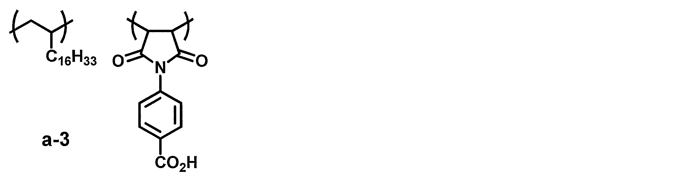
撹拌羽、還流冷却管、温度計を取り付けた三口フラスコ中に、ポリ(マレイン酸無水物-alt-1-オクタデセン)(アルドリッチ製、17.92g)、p-アミノ安息香酸(和光純薬製、7.54g)、N,N-ジメチルアセトアミド(和光純薬製、40g)を入れ、80℃で1時間撹拌した。次いで、酢酸(和光純薬製、25.04g)を加え、120℃で9時間撹拌した。得られた溶液を室温まで冷却後、メタノール/水(50/50(質量比))に滴下した。析出した固体をろ取した後、真空乾燥機で乾燥することにより、a-3を得た。得られたa-3の構造は1H NMRにより同定した。a-3のGPCを測定したところ、ポリスチレン換算でMw=50000であった。
(合成例4)マレイミド系重合体(a-4)の合成

撹拌羽、還流冷却管、温度計を取り付けた三口フラスコ中に、ポリ(メチルビニルエーテル-alt-マレイン酸無水物)(アルドリッチ製、8.51g)、p-アミノ安息香酸(和光純薬製、7.54g)、N,N-ジメチルアセトアミド(和光純薬製、40g)を入れ、80℃で1時間撹拌した。次いで、酢酸(和光純薬製、25.04g)を加え、120℃で9時間撹拌した。得られた溶液を室温まで冷却後、メタノール/水(50/50(質量比))に滴下した。析出した固体をろ取した後、真空乾燥機で乾燥することにより、a-4を得た。得られたa-4の構造は1H NMRにより同定した。a-4のGPCを測定したところ、ポリスチレン換算でMw=230000であった。
(合成例5)マレイミド系重合体(a-5)の合成
撹拌羽、還流冷却管、温度計を取り付けた三口フラスコ中に、SMA3000(Cray Valley製、8.21g)、β-アラニン(東京化成工業製、1.87g)、N,N-ジメチルアセトアミド(和光純薬製、35g)を入れ、80℃で1時間撹拌した。次いで、酢酸(和光純薬製、10.03g)を加え、120℃で9時間撹拌した。得られた溶液を室温まで冷却後、メタノール/水(50/50(質量比))に滴下した。析出した固体をろ取した後、真空乾燥機で乾燥することにより、a-5を得た。得られたa-5の構造は1H NMRにより同定した。a-5のGPCを測定したところ、ポリスチレン換算でMw=11000であった。
(合成例6)マレイミド系重合体(a-6)の合成
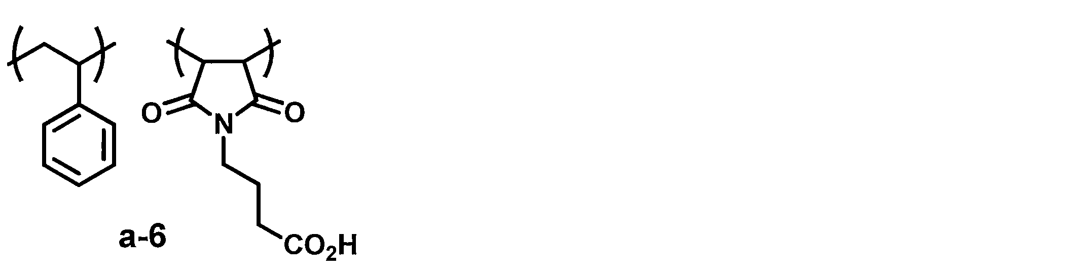
撹拌羽、還流冷却管、温度計を取り付けた三口フラスコ中に、SMA3000(Cray Valley製、8.21g)、4-アミノブタン酸(東京化成工業製、2.17g)、N,N-ジメチルアセトアミド(和光純薬製、35g)を入れ、80℃で1時間撹拌した。次いで、酢酸(和光純薬製、10.03g)を加え、120℃で9時間撹拌した。得られた溶液を室温まで冷却後、メタノール/水(50/50(質量比))に滴下した。析出した固体をろ取した後、真空乾燥機で乾燥することにより、a-6を得た。得られたa-6の構造は1H NMRにより同定した。a-6のGPCを測定したところ、ポリスチレン換算でMw=12000であった。
(合成例7)マレイミド系重合体(a-7)の合成
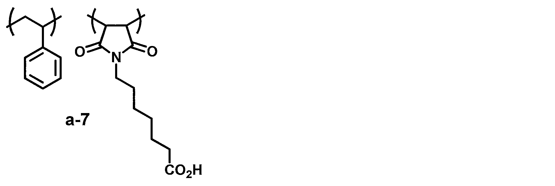
撹拌羽、還流冷却管、温度計を取り付けた三口フラスコ中に、SMA3000(Cray Valley製、8.21g)、7-アミノヘプタン酸(東京化成工業製、3.05g)、N,N-ジメチルアセトアミド(和光純薬製、35g)を入れ、80℃で1時間撹拌した。次いで、酢酸(和光純薬製、10.03g)を加え、120℃で9時間撹拌した。得られた溶液を室温まで冷却後、メタノール/水(50/50(質量比))に滴下した。析出した固体をろ取した後、真空乾燥機で乾燥することにより、a-7を得た。得られたa-7の構造は1H NMRにより同定した。a-7のGPCを測定したところ、ポリスチレン換算でMw=14000であった。
(合成例8)マレイミド系重合体(a-8)の合成

撹拌羽、還流冷却管、温度計を取り付けた三口フラスコ中に、SMA3000(Cray Valley製、8.21g)、4-アミノフタル酸(東京化成工業製、3.80g)、N,N-ジメチルアセトアミド(和光純薬製、35g)を入れ、80℃で1時間撹拌した。次いで、酢酸(和光純薬製、10.03g)を加え、120℃で9時間撹拌した。得られた溶液を室温まで冷却後、メタノール/水(50/50(質量比))に滴下した。析出した固体をろ取した後、真空乾燥機で乾燥することにより、a-8を得た。得られたa-8の構造は1H NMRにより同定した。a-8のGPCを測定したところ、ポリスチレン換算でMw=14000であった。
(合成例9)マレイミド系重合体(a-9)の合成
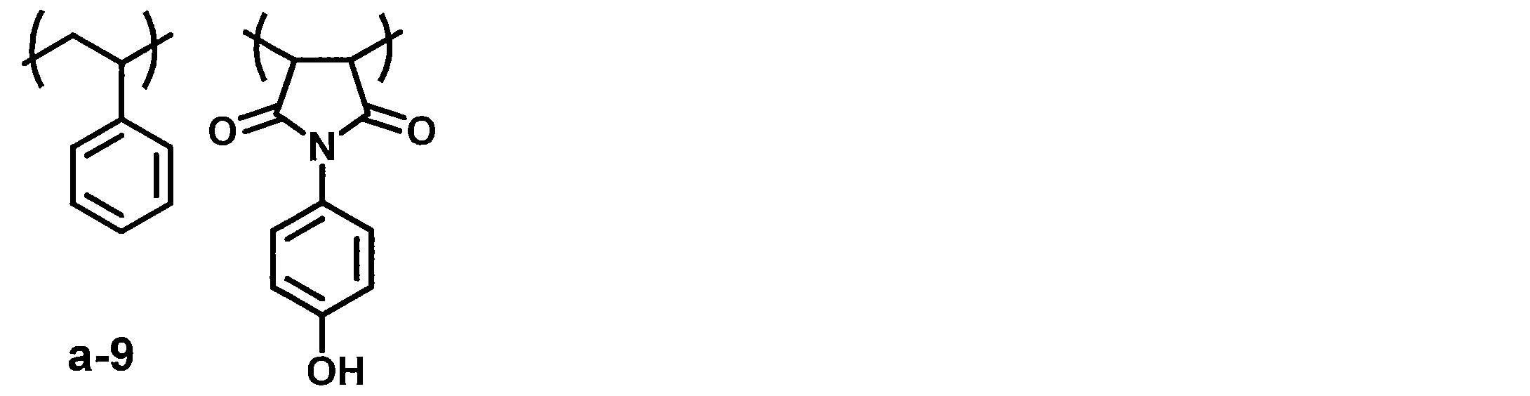
撹拌羽、還流冷却管、温度計を取り付けた三口フラスコ中に、SMA3000(Cray Valley製、8.21g)、4-アミノフェノール(東京化成工業製、2.29g)、N,N-ジメチルアセトアミド(和光純薬製、35g)を入れ、80℃で1時間撹拌した。次いで、酢酸(和光純薬製、10.03g)を加え、120℃で9時間撹拌した。得られた溶液を室温まで冷却後、メタノール/水(50/50(質量比))に滴下した。析出した固体をろ取した後、真空乾燥機で乾燥することにより、a-9を得た。得られたa-9の構造は1H NMRにより同定した。a-9のGPCを測定したところ、ポリスチレン換算でMw=12000であった。
(合成例10)マレイミド系重合体(a-10)の合成
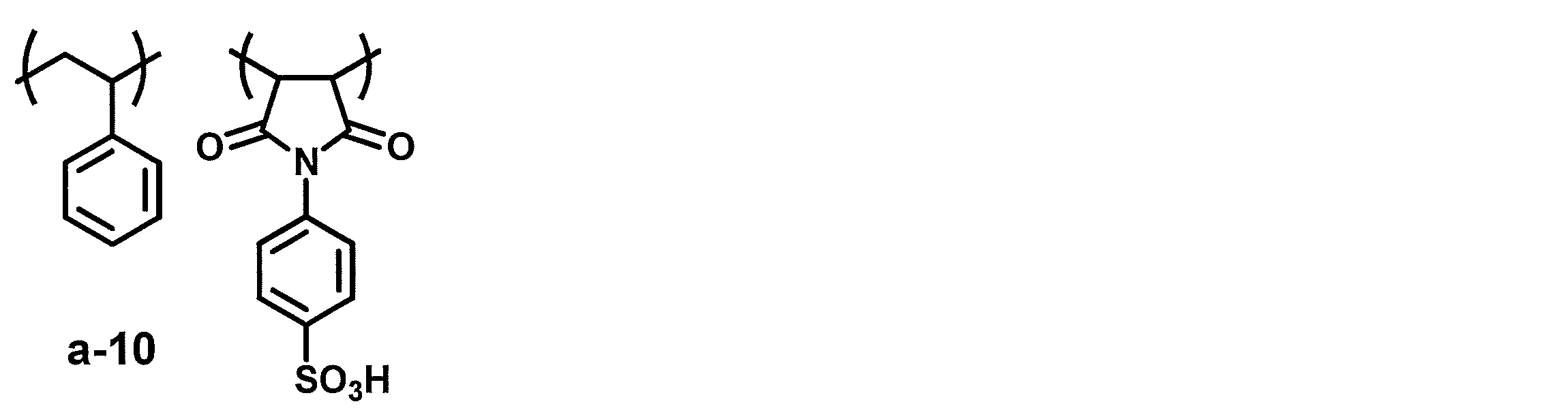
撹拌羽、還流冷却管、温度計を取り付けた三口フラスコ中に、SMA3000(Cray Valley製、8.21g)、スルファニル酸(東京化成工業製、3.64g)、N,N-ジメチルアセトアミド(和光純薬製、35g)を入れ、80℃で1時間撹拌した。次いで、酢酸(和光純薬製、10.03g)を加え、120℃で9時間撹拌した。得られた溶液を室温まで冷却後、メタノール/水(50/50(質量比))に滴下した。析出した固体をろ取した後、真空乾燥機で乾燥することにより、a-10を得た。得られたa-10の構造は1H NMRにより同定した。a-10のGPCを測定したところ、ポリスチレン換算でMw=14000であった。
(合成例11)マレイミド系重合体(a-1-2)の合成

撹拌羽、還流冷却管、温度計を取り付けた三口フラスコ中に、SMA1000(Cray Valley製、10.11g)、p-アミノ安息香酸(和光純薬製、5.67g)、N,N-ジメチルアセトアミド(和光純薬製、50g)を入れ、80℃で1時間撹拌した。次いで、酢酸(和光純薬製、25.04g)を加え、120℃で9時間撹拌した。得られた溶液を室温まで冷却後、メタノール/水(50/50(質量比))に滴下した。析出した固体をろ取した後、真空乾燥機で乾燥することにより、a-1-2を得た。得られたa-1-2の構造は1H NMRにより同定した。a-1-2のGPCを測定したところ、ポリスチレン換算でMw=6800であった。
(合成例12)マレイミド系重合体(a-1-3)の合成
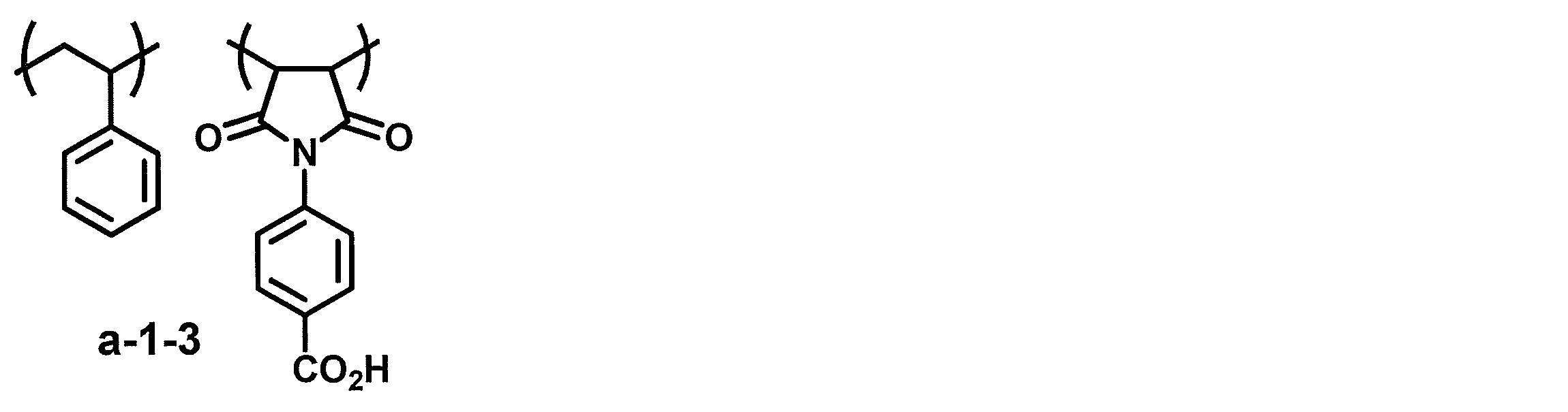
撹拌羽、還流冷却管、温度計を取り付けた三口フラスコ中に、SMA2000(Cray Valley製、6.13g)、p-アミノ安息香酸(和光純薬製、2.88g)、N,N-ジメチルアセトアミド(和光純薬製、30g)を入れ、80℃で1時間撹拌した。次いで、酢酸(和光純薬製、10.03g)を加え、120℃で9時間撹拌した。得られた溶液を室温まで冷却後、メタノール/水(50/50(質量比))に滴下した。析出した固体をろ取した後、真空乾燥機で乾燥することにより、a-1-3を得た。得られたa-1-3の構造は1H NMRにより同定した。a-1-3のGPCを測定したところ、ポリスチレン換算でMw=9200であった。
(合成例13)マレイミド系重合体(a-1-4)の合成
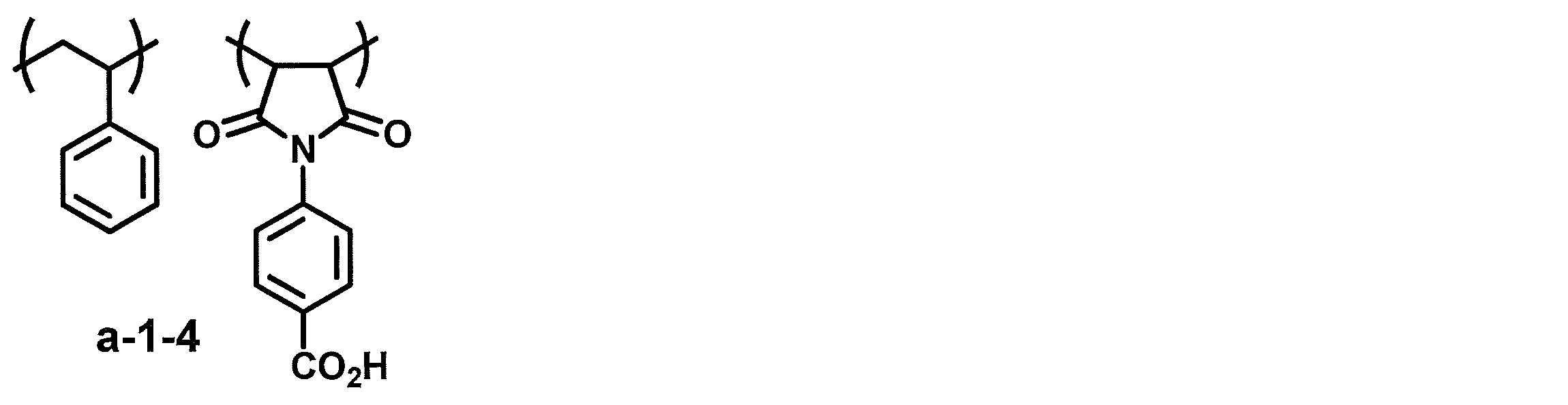
撹拌羽、還流冷却管、温度計を取り付けた三口フラスコ中に、SMA2021(Cray Valley製、6.13g)、p-アミノ安息香酸(和光純薬製、2.88g)、N,N-ジメチルアセトアミド(和光純薬製、30g)を入れ、80℃で1時間撹拌した。次いで、酢酸(和光純薬製、10.03g)を加え、120℃で9時間撹拌した。得られた溶液を室温まで冷却後、メタノール/水(50/50(質量比))に滴下した。析出した固体をろ取した後、真空乾燥機で乾燥することにより、a-1-4を得た。得られたa-1-4の構造は1H NMRにより同定した。a-1-4のGPCを測定したところ、ポリスチレン換算でMw=30000であった。
(合成例14)マレイミド系重合体(a-1-5)の合成

撹拌羽、還流冷却管、温度計を取り付けた三口フラスコ中に、SMA E40(Cray Valley製、6.13g)、p-アミノ安息香酸(和光純薬製、1.80g)、N,N-ジメチルアセトアミド(和光純薬製、30g)を入れ、80℃で1時間撹拌した。次いで、酢酸(和光純薬製、10.03g)を加え、120℃で9時間撹拌した。得られた溶液を室温まで冷却後、メタノール/水(50/50(質量比))に滴下した。析出した固体をろ取した後、真空乾燥機で乾燥することにより、a-1-5を得た。得られたa-1-5の構造は1H NMRにより同定した。a-1-5のGPCを測定したところ、ポリスチレン換算でMw=30000であった。
(合成例15)マレイミド系重合体(a-1-6)の合成
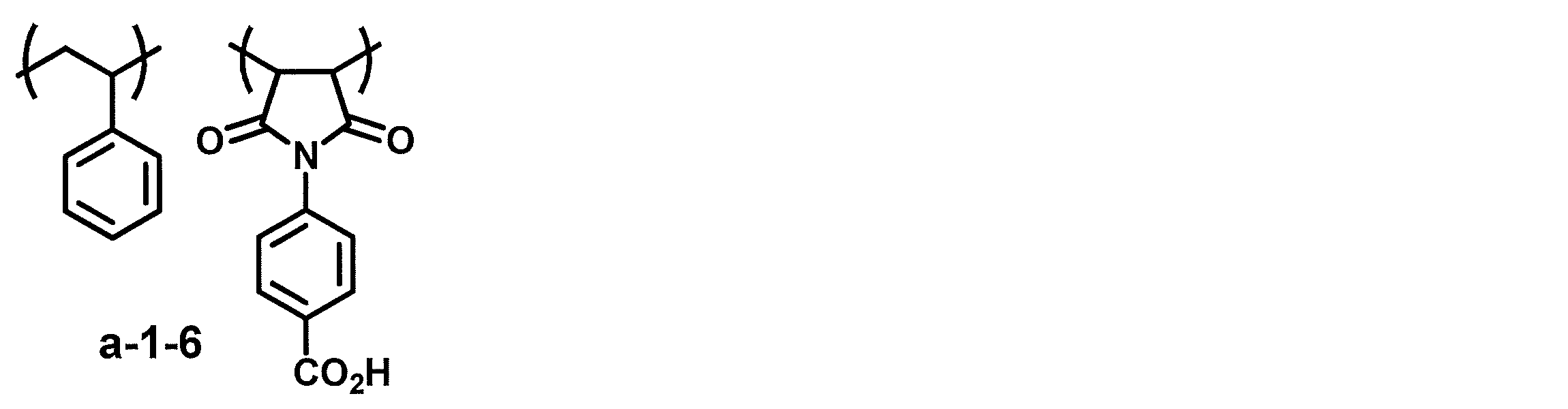
撹拌羽、還流冷却管、温度計を取り付けた三口フラスコ中に、SMA E60(Cray Valley製、6.13g)、p-アミノ安息香酸(和光純薬製、1.28g)、N,N-ジメチルアセトアミド(和光純薬製、30g)を入れ、80℃で1時間撹拌した。次いで、酢酸(和光純薬製、10.03g)を加え、120℃で9時間撹拌した。得られた溶液を室温まで冷却後、メタノール/水(50/50(質量比))に滴下した。析出した固体をろ取した後、真空乾燥機で乾燥することにより、a-1-6を得た。得られたa-1-6の構造は1H NMRにより同定した。a-1-6のGPCを測定したところ、ポリスチレン換算でMw=30000であった。
(合成例16)ポリイミド(p-1)の合成

撹拌羽、還流冷却管、温度計を取り付けた三口フラスコ中に、3,5-ジアミノ安息香酸(東京化成工業製、1.89g)、脂肪族エーテルジアミン D-400(BASF製、15.21g)、1,1,3,3-テトラメチル-1,3-ビス(4-アミノフェニル)ジシロキサン LP-7100(信越化学製、0.39g)、及びN-メチル-2-ピロリジノン(和光純薬製、116g)を入れた。次いで、4,4'-オキシジフタル酸二無水物(和光純薬製、16.88g)を、上記フラスコを氷浴中で冷却しながら、フラスコ内に少量ずつ添加した。添加終了後、さらに室温で5時間攪拌した。次に、フラスコに水分受容器付の還流冷却器を取り付け、キシレン70gを加え、窒素ガスを吹き込みながら180℃に昇温させてその温度を5時間保持し、水と共にキシレンを共沸除去した。得られた溶液を室温まで冷却後、蒸留水中に滴下した。析出した固体をろ取した後、真空乾燥機で乾燥することにより、p-1を得た。得られたp-1の構造は1H NMRにより同定した。p-1のGPCを測定したところ、ポリスチレン換算でMw=33000であった。なお、上記構造式の「Y」は、ポリエーテルを表す。
(合成例17)アクリル酸-フェニルマレイミド共重合体(p-3)の合成
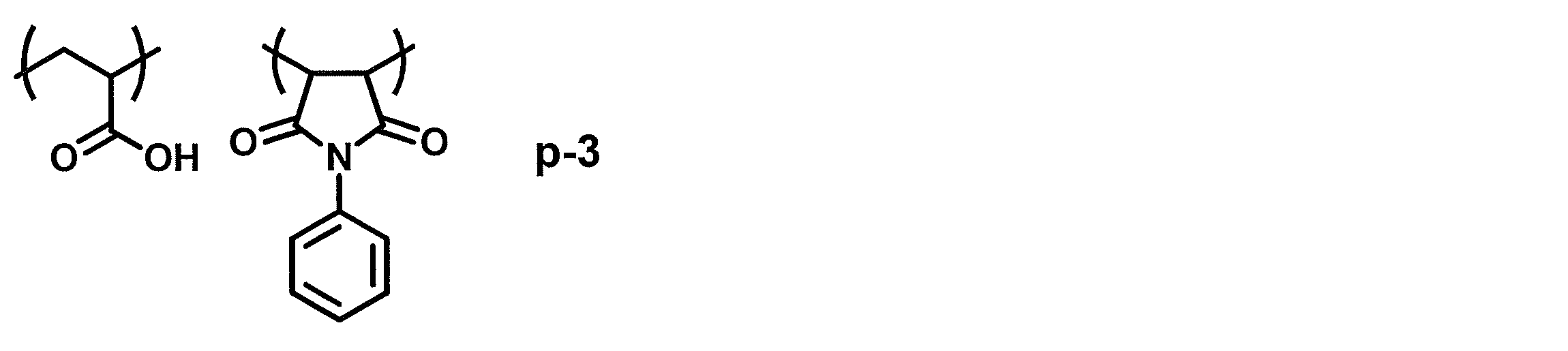
撹拌羽、還流冷却管、温度計を取り付けた三口フラスコ中に、アクリル酸(和光純薬製、7.21g)、N-フェニルマレイミド(東京化成工業製、17.32g)、N,N-ジメチルホルムアミド(和光純薬製、82g)を加え、室温で均一に溶解させた。次いで、アゾビスイソブチロニトリル(AIBN)(和光純薬製、1.64g)を添加した。窒素ガスを吹き込みながら70℃に昇温し、6時間撹拌させた。得られた溶液を室温まで冷却後、蒸留水中に滴下した。 析出した固体をろ取した後、真空乾燥機で乾燥することにより、p-3を得た。得られたp-3の構造は1H NMRにより同定した。p-3のGPCを測定したところ、ポリスチレン換算でMw=30000であった。
(合成例18)p-ヒドロキシスチレン-フェニルマレイミド共重合体(p-4)の合成

撹拌羽、還流冷却管、温度計を取り付けた三口フラスコ中に、p-(tert)-ブトキシ)スチレン(和光純薬製、9.75g)、N-フェニルマレイミド(東京化成工業製、9.52g)、N,N-ジメチルホルムアミド(和光純薬製、50g)を加え、室温で均一に溶解させた。次いで、アゾビスイソブチロニトリル(AIBN)(和光純薬製、0.13g)を添加した。窒素ガスを吹き込みながら70℃に昇温し、6時間撹拌させた。次いで、濃塩酸(和光純薬製、6.20g)を添加し、70℃でさらに3時間加熱した。得られた溶液を室温まで冷却後、蒸留水中に滴下した。析出した固体をろ取した後、真空乾燥機で乾燥することにより、p-4を得た。得られたp-4の構造は1H NMRにより同定した。p-4のGPCを測定したところ、ポリスチレン換算でMw=20000であった。
[実施例1~46、比較例1~7]
下記記載の成分を混合し、液状の感光性樹脂組成物を調製した。
なお、実施例37においては、光重合開始剤の含有量を0.5質量部とした。また、実施例38においては、光重合開始剤の含有量を0.2質量部とした。また、実施例39においては、熱重合開始剤の含有量を0.2質量部とした。また、実施例40においては、光重合開始剤の含有量を0.1質量部とした。
<感光性樹脂組成物の組成>
(a)重合体:75質量部
(b)架橋剤:25質量部
(c)光重合開始剤:2質量部
(d)溶剤:160質量部
(e)熱重合開始剤:1質量部
(f)フィラー:10質量部
(g)密着性付与剤:5質量部
下記記載の成分を混合し、液状の感光性樹脂組成物を調製した。
なお、実施例37においては、光重合開始剤の含有量を0.5質量部とした。また、実施例38においては、光重合開始剤の含有量を0.2質量部とした。また、実施例39においては、熱重合開始剤の含有量を0.2質量部とした。また、実施例40においては、光重合開始剤の含有量を0.1質量部とした。
<感光性樹脂組成物の組成>
(a)重合体:75質量部
(b)架橋剤:25質量部
(c)光重合開始剤:2質量部
(d)溶剤:160質量部
(e)熱重合開始剤:1質量部
(f)フィラー:10質量部
(g)密着性付与剤:5質量部
<重合体の300℃での重量減少量>
各重合体を、熱分析装置(TGA)(Q500、TA Instruments製)を用いて、窒素気流下、昇温速度20℃/minにて500℃まで昇温することで、300℃での重量減少率を求めた。
各重合体を、熱分析装置(TGA)(Q500、TA Instruments製)を用いて、窒素気流下、昇温速度20℃/minにて500℃まで昇温することで、300℃での重量減少率を求めた。
<耐熱性の評価>
各感光性樹脂組成物を、乾燥後の膜厚が20μmとなるようにシリコンウエハ(4インチ径、厚さ525μm)上にスピンコートにて塗布し、140℃で5分間加熱した。次いで、平行露光機を用いて1000mJ/cm2(波長:365nm)で露光し、感光性樹脂組成物を硬化させた。熱分析装置(TGA)(Q500、TA Instruments製)を用いて、窒素気流下、昇温速度20℃/minにて500℃まで昇温することで、300℃での重量減少率を求めた。以下の基準で耐熱性を評価した。以下の基準で2~5が実用的であり、3~5が好ましく、4~5が特に好ましい。
5:重量減少率が1%未満
4:重量減少率が1%以上5%未満
3:重量減少率が5%以上10%未満
2:重量減少率が10%以上15%未満
1:重量減少率が15%以上
各感光性樹脂組成物を、乾燥後の膜厚が20μmとなるようにシリコンウエハ(4インチ径、厚さ525μm)上にスピンコートにて塗布し、140℃で5分間加熱した。次いで、平行露光機を用いて1000mJ/cm2(波長:365nm)で露光し、感光性樹脂組成物を硬化させた。熱分析装置(TGA)(Q500、TA Instruments製)を用いて、窒素気流下、昇温速度20℃/minにて500℃まで昇温することで、300℃での重量減少率を求めた。以下の基準で耐熱性を評価した。以下の基準で2~5が実用的であり、3~5が好ましく、4~5が特に好ましい。
5:重量減少率が1%未満
4:重量減少率が1%以上5%未満
3:重量減少率が5%以上10%未満
2:重量減少率が10%以上15%未満
1:重量減少率が15%以上
<現像性の評価>
各感光性樹脂組成物を、乾燥後の膜厚が20μmとなるようにシリコンウエハ(4インチ径、厚さ525μm)上にスピンコートにて塗布し、140℃で5分間加熱した。次いで、50μm径のドットが配置されたマスクを介して、平行露光機を用いて1000mJ/cm2(波長:365nm)で露光した。次いで、水酸化テトラメチルアンモニウム2.38重量%水溶液に1分間浸漬し、さらに水洗することで現像した。現像後のホールパターンを光学顕微鏡にて観察し、以下の基準で現像性を評価した。以下の基準で3~5が実用的であり、4~5が特に好ましい。
5:残膜無くホールパターンが得られた
4:残膜は50%未満存在するがホールパターンが得られた
3:残膜は50%以上存在するがホールパターンが得られた
2:パターンは形成されているがほとんど現像されていない
1:パターンが全く形成されていない
各感光性樹脂組成物を、乾燥後の膜厚が20μmとなるようにシリコンウエハ(4インチ径、厚さ525μm)上にスピンコートにて塗布し、140℃で5分間加熱した。次いで、50μm径のドットが配置されたマスクを介して、平行露光機を用いて1000mJ/cm2(波長:365nm)で露光した。次いで、水酸化テトラメチルアンモニウム2.38重量%水溶液に1分間浸漬し、さらに水洗することで現像した。現像後のホールパターンを光学顕微鏡にて観察し、以下の基準で現像性を評価した。以下の基準で3~5が実用的であり、4~5が特に好ましい。
5:残膜無くホールパターンが得られた
4:残膜は50%未満存在するがホールパターンが得られた
3:残膜は50%以上存在するがホールパターンが得られた
2:パターンは形成されているがほとんど現像されていない
1:パターンが全く形成されていない
<硬化性の評価>
各感光性樹脂組成物を、乾燥後の膜厚が20μmとなるようにシリコンウエハ(4インチ径、厚さ525μm)上にスピンコートにて塗布し、140℃で5分間加熱した。次いで、平行露光機を用いて1000mJ/cm2(波長:365nm)で露光し、感光性樹脂組成物を半硬化させた。次いで、ホットプレート上で180℃に加熱して表面をスパチュラで擦り、跡が付かなくなるまでの時間を測定した。以下の基準で硬化性を評価した。以下の基準で2~5が実用的であり、3~5が好ましく、4~5が特に好ましい。
5:5分以内に跡が付かなくなった
4:5分を超え10分以内に跡が付かなくなった
3:10分を超え15分以内に跡が付かなくなった
2:15分を超え20分以内に跡が付かなくなった
1:跡が付かなくなるまでに20分を超えた
各感光性樹脂組成物を、乾燥後の膜厚が20μmとなるようにシリコンウエハ(4インチ径、厚さ525μm)上にスピンコートにて塗布し、140℃で5分間加熱した。次いで、平行露光機を用いて1000mJ/cm2(波長:365nm)で露光し、感光性樹脂組成物を半硬化させた。次いで、ホットプレート上で180℃に加熱して表面をスパチュラで擦り、跡が付かなくなるまでの時間を測定した。以下の基準で硬化性を評価した。以下の基準で2~5が実用的であり、3~5が好ましく、4~5が特に好ましい。
5:5分以内に跡が付かなくなった
4:5分を超え10分以内に跡が付かなくなった
3:10分を超え15分以内に跡が付かなくなった
2:15分を超え20分以内に跡が付かなくなった
1:跡が付かなくなるまでに20分を超えた
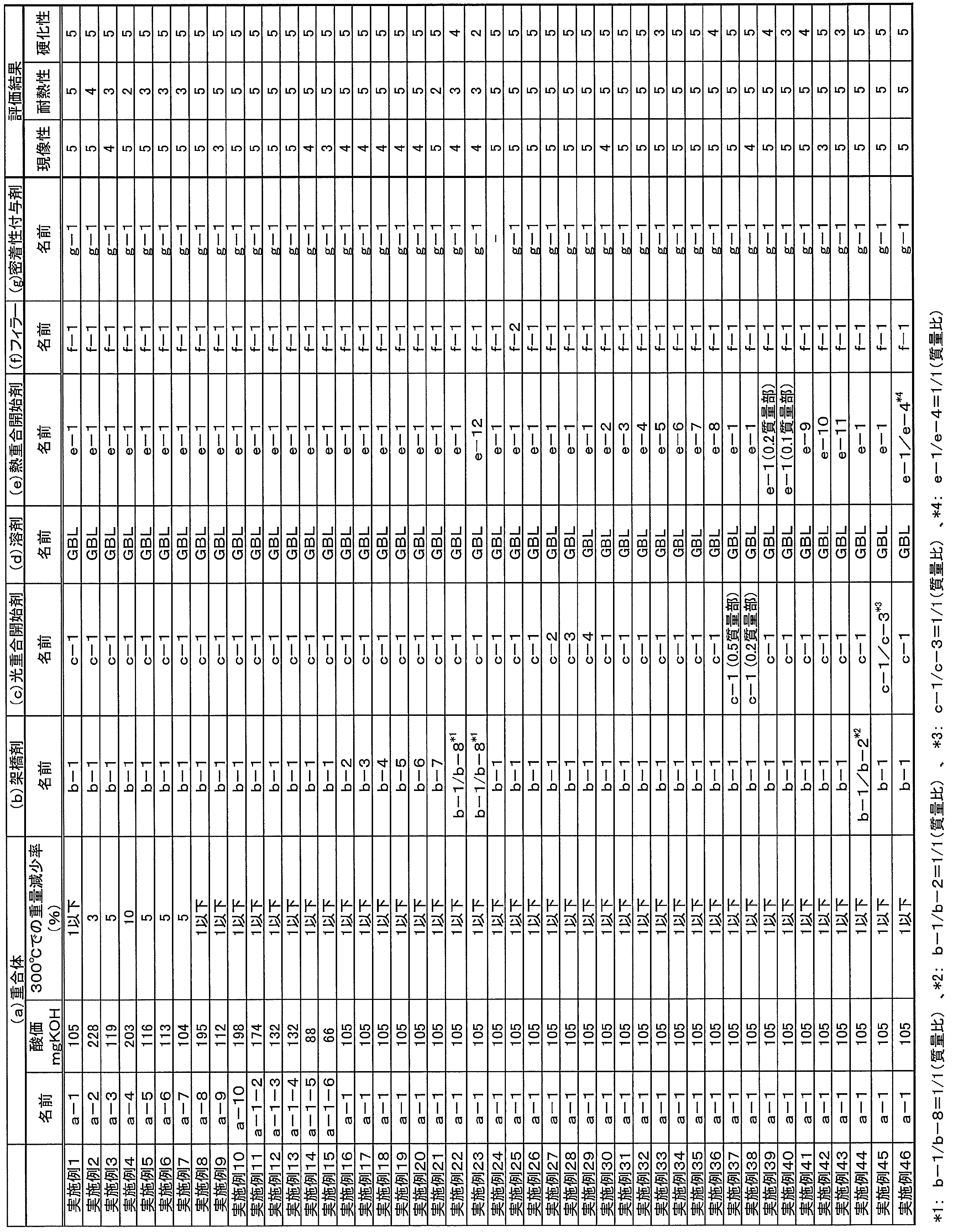
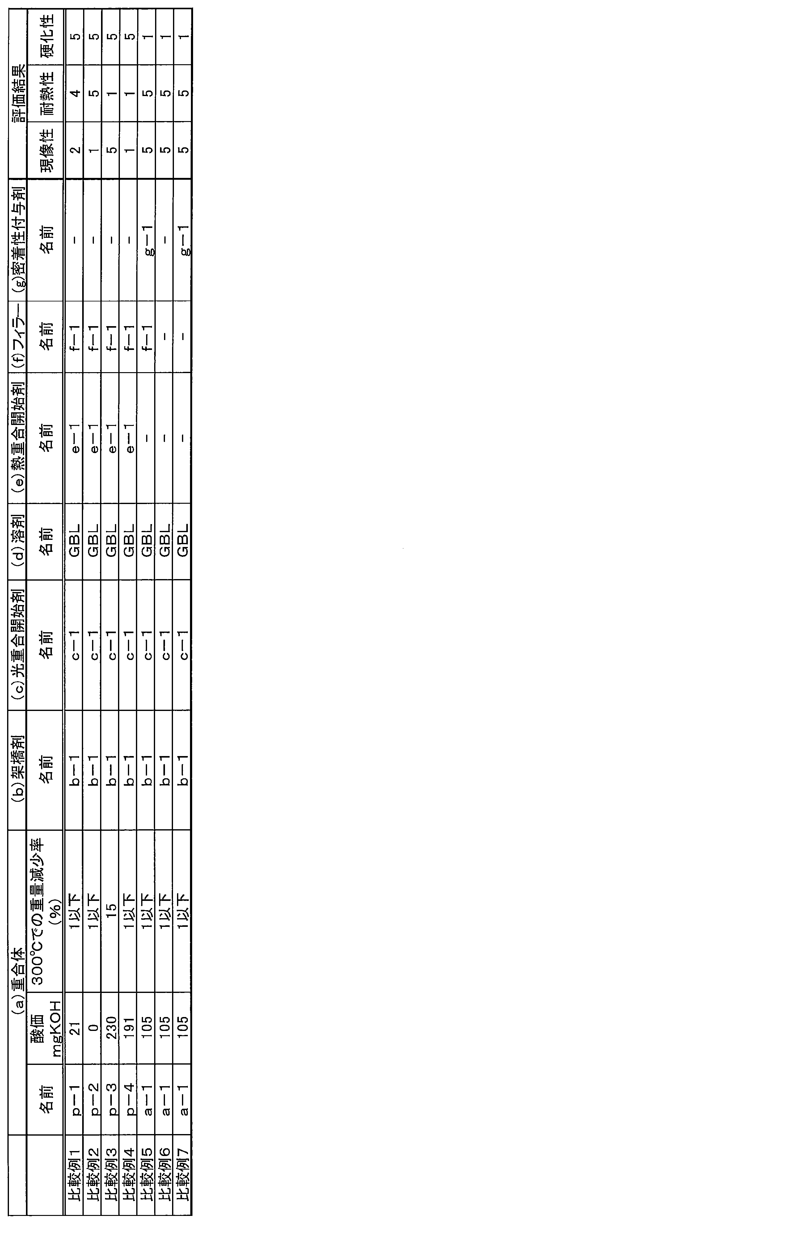
上記結果より、実施例1~46の感光性樹脂組成物は、現像性、耐熱性および硬化性が良好で、いずれも実用レベルであった。
一方、比較例1~7の感光性樹脂組成物は、現像性、耐熱性および硬化性の少なくとも一つにおいて、実用レベルを満たさないものがあった。
一方、比較例1~7の感光性樹脂組成物は、現像性、耐熱性および硬化性の少なくとも一つにおいて、実用レベルを満たさないものがあった。
表1に記載した略称は以下の通りである。
(a)重合体
a-1~a-10、a-1-2~a-1-6、p-1、p-3、p-4:合成例1~18で得られたa-1~a-10、a-1-2~a-1-6、p-1、p-3、p-4
p-2:スチレン-フェニルマレイミド共重合体 ポリイミレックスPSX0371(日本触媒製) 下記構造
a-1~a-10、a-1-2~a-1-6、p-1、p-3、p-4:合成例1~18で得られたa-1~a-10、a-1-2~a-1-6、p-1、p-3、p-4
p-2:スチレン-フェニルマレイミド共重合体 ポリイミレックスPSX0371(日本触媒製) 下記構造
(b)架橋剤
b-1:A-9300(新中村化学工業製) エチレン性不飽和化合物
b-2:A-TMPT(新中村化学工業製) エチレン性不飽和化合物
b-3:A-TMMT(新中村化学工業製) エチレン性不飽和化合物
b-4:AD-TMP(新中村化学工業製) エチレン性不飽和化合物
b-5:A-DPH(新中村化学工業製) エチレン性不飽和化合物
b-6:A-BPE-4(新中村化学工業製) エチレン性不飽和化合物
b-7:4G(新中村化学工業製) エチレン性不飽和化合物
b-8:BEO-60E(新日本理化製) エポキシ化合物
b-1:A-9300(新中村化学工業製) エチレン性不飽和化合物
b-2:A-TMPT(新中村化学工業製) エチレン性不飽和化合物
b-3:A-TMMT(新中村化学工業製) エチレン性不飽和化合物
b-4:AD-TMP(新中村化学工業製) エチレン性不飽和化合物
b-5:A-DPH(新中村化学工業製) エチレン性不飽和化合物
b-6:A-BPE-4(新中村化学工業製) エチレン性不飽和化合物
b-7:4G(新中村化学工業製) エチレン性不飽和化合物
b-8:BEO-60E(新日本理化製) エポキシ化合物
(c)光重合開始剤
c-1:N-1919(ADEKA製)
c-2:IRGACURE-184(BASF社製)
c-3:IRGACURE-OXE01(BASF社製)
c-4:IRGACURE-OXE02(BASF社製)
c-1:N-1919(ADEKA製)
c-2:IRGACURE-184(BASF社製)
c-3:IRGACURE-OXE01(BASF社製)
c-4:IRGACURE-OXE02(BASF社製)
(d)溶剤
GBL:γ-ブチロラクトン(和光純薬工業製)
GBL:γ-ブチロラクトン(和光純薬工業製)
(e)熱重合開始剤
e-1:パークミルD(日油製、熱ラジカル発生剤、分子量270.38、1分間半減期温度175.2℃)
e-2:パーブチルZ(日油製、熱ラジカル発生剤、分子量194.23、1分間半減期温度166.8℃)
e-3:パーヘキサV(日油製、熱ラジカル発生剤、分子量334.46、1分間半減期温度172.5℃)
e-4:パーブチルP(日油製、熱ラジカル発生剤、分子量338.49、1分間半減期温度175.4℃)
e-5:パーブチルD(日油製、熱ラジカル発生剤、分子量146.23、1分間半減期温度185.9℃)
e-6:パーヘキサ25B(日油製、熱ラジカル発生剤、分子量290.45、1分間半減期温度179.8℃)
e-7:パーヘキシン25B(日油製、熱ラジカル発生剤、分子量286.42、1分間半減期温度194.3℃)
e-8:パークミルP(日油製、熱ラジカル発生剤、分子量194.28、1分間半減期温度232.5℃)
e-9:パーメタンH(日油製、熱ラジカル発生剤、分子量172.27、1分間半減期温度199.5℃)
e-10:パーヘキサHC(日油製、熱ラジカル発生剤、分子量316.47、1分間半減期温度149.2℃)
e-11:パークミルH(日油製、熱ラジカル発生剤、分子量152.20、1分間半減期温度254.0℃)
e-12:p-トルエンスルホン酸シクロヘキシル(東京化成工業製、熱酸発生剤)
e-1:パークミルD(日油製、熱ラジカル発生剤、分子量270.38、1分間半減期温度175.2℃)
e-2:パーブチルZ(日油製、熱ラジカル発生剤、分子量194.23、1分間半減期温度166.8℃)
e-3:パーヘキサV(日油製、熱ラジカル発生剤、分子量334.46、1分間半減期温度172.5℃)
e-4:パーブチルP(日油製、熱ラジカル発生剤、分子量338.49、1分間半減期温度175.4℃)
e-5:パーブチルD(日油製、熱ラジカル発生剤、分子量146.23、1分間半減期温度185.9℃)
e-6:パーヘキサ25B(日油製、熱ラジカル発生剤、分子量290.45、1分間半減期温度179.8℃)
e-7:パーヘキシン25B(日油製、熱ラジカル発生剤、分子量286.42、1分間半減期温度194.3℃)
e-8:パークミルP(日油製、熱ラジカル発生剤、分子量194.28、1分間半減期温度232.5℃)
e-9:パーメタンH(日油製、熱ラジカル発生剤、分子量172.27、1分間半減期温度199.5℃)
e-10:パーヘキサHC(日油製、熱ラジカル発生剤、分子量316.47、1分間半減期温度149.2℃)
e-11:パークミルH(日油製、熱ラジカル発生剤、分子量152.20、1分間半減期温度254.0℃)
e-12:p-トルエンスルホン酸シクロヘキシル(東京化成工業製、熱酸発生剤)
(f)フィラー
f-1:R-972(シリカ、日本アエロジル製)
f-2:AKP-50(アルミナ、住友化学製)
f-1:R-972(シリカ、日本アエロジル製)
f-2:AKP-50(アルミナ、住友化学製)
(g)密着性付与剤
g-1:KBE-503(3-メタクリロキシプロピルトリエトキシシラン、信越シリコーン製)
g-1:KBE-503(3-メタクリロキシプロピルトリエトキシシラン、信越シリコーン製)
1:フィルム状接着剤
1a:接着層パターン
2:カバーフィルム
3:樹脂フィルム
6:粘着剤層
7:樹脂フィルム
8:半導体ウエハ
11:接着層
11a:アンダーフィル層
12、12a、12b:半導体素子
13:半導体素子搭載用支持部材
14:ワイヤ
15:封止材
16:端子
20、20a、20b:接着層付半導体ウエハ
100、110、120:接着シート
200、210、300:半導体デバイス
301a~301d:半導体素子
301:半導体素子積層体
302b~302d:貫通電極
303a~303e:金属バンプ
305:再配線層
310、310a、310b:アンダーフィル層
315:絶縁層
320:半導体素子搭載用支持部材
320a:表面電極
1a:接着層パターン
2:カバーフィルム
3:樹脂フィルム
6:粘着剤層
7:樹脂フィルム
8:半導体ウエハ
11:接着層
11a:アンダーフィル層
12、12a、12b:半導体素子
13:半導体素子搭載用支持部材
14:ワイヤ
15:封止材
16:端子
20、20a、20b:接着層付半導体ウエハ
100、110、120:接着シート
200、210、300:半導体デバイス
301a~301d:半導体素子
301:半導体素子積層体
302b~302d:貫通電極
303a~303e:金属バンプ
305:再配線層
310、310a、310b:アンダーフィル層
315:絶縁層
320:半導体素子搭載用支持部材
320a:表面電極
Claims (18)
- 酸基含有マレイミドに由来する繰り返し単位を含む重合体と、架橋剤と、光重合開始剤と、熱重合開始剤とを含む感光性樹脂組成物。
- 前記重合体が、さらに、ビニル化合物に由来する繰り返し単位を含む、請求項1に記載の感光性樹脂組成物。
- さらに溶剤を含む、請求項1または2に記載の感光性樹脂組成物。
- 前記架橋剤が、エチレン性不飽和結合を有する基を2個以上有する化合物である、請求項1~3のいずれか1項に記載の感光性樹脂組成物。
- 前記架橋剤が、下記式で表される部分構造を有する、請求項1~4のいずれか1項に記載の感光性樹脂組成物;ただし、式中の*は連結手である。

- 前記重合体が、下記一般式(1)で表される繰り返し単位と、下記一般式(2)で表される繰り返し単位とを含む重合体である、請求項1~5のいずれか1項に記載の感光性樹脂組成物;

- 前記重合体の酸価が50mgKOH/g以上である、請求項1~6のいずれか1項に記載の感光性樹脂組成物。
- 前記重合体は、20℃/分で昇温したときの300℃における重量減少率が5%以下である、請求項1~7のいずれか1項に記載の感光性樹脂組成物。
- さらにフィラーを含む、請求項1~8のいずれか1項に記載の感光性樹脂組成物。
- さらに密着性付与剤を含む、請求項1~9のいずれか1項に記載の感光性樹脂組成物。
- アンダーフィル用である、請求項1~10のいずれか1項に記載の感光性樹脂組成物。
- 液状である、請求項1~11のいずれか1項に記載の感光性樹脂組成物。
- シート状である、請求項1~11のいずれか1項に記載の感光性樹脂組成物。
- 半導体ウエハの表面に、請求項1~13のいずれか1項に記載の感光性樹脂組成物からなる層を有する積層体。
- 半導体ウエハの表面に、請求項1~13のいずれか1項に記載の感光性樹脂組成物を硬化してなる硬化物層を有する積層体。
- 請求項12に記載の感光性樹脂組成物を半導体ウエハに適用する工程と、
半導体ウエハに適用された感光性樹脂組成物を乾燥させる工程と、
乾燥された感光性樹脂組成物を露光する工程と、
露光された感光性樹脂組成物を現像する工程と、
現像された感光性樹脂組成物の表面に、被着体を加熱圧着する工程と、
を含む半導体デバイスの製造方法。 - 請求項13に記載の感光性樹脂組成物を半導体ウエハに積層する工程と、
半導体ウエハに積層された感光性樹脂組成物を露光する工程と、
露光された感光性樹脂組成物を現像する工程と、
現像された感光性樹脂組成物の表面に、被着体を加熱圧着する工程と、
を含む半導体デバイスの製造方法。 - 請求項16または17に記載の方法で製造された半導体デバイス。
Priority Applications (1)
| Application Number | Priority Date | Filing Date | Title |
|---|---|---|---|
| US15/275,787 US20170012022A1 (en) | 2014-03-28 | 2016-09-26 | Photosensitive resin composition, laminate, method for manufacturing semiconductor device, and semiconductor device |
Applications Claiming Priority (2)
| Application Number | Priority Date | Filing Date | Title |
|---|---|---|---|
| JP2014069007A JP6234864B2 (ja) | 2014-03-28 | 2014-03-28 | 感光性樹脂組成物、積層体、半導体デバイスの製造方法、半導体デバイス |
| JP2014-069007 | 2014-03-28 |
Related Child Applications (1)
| Application Number | Title | Priority Date | Filing Date |
|---|---|---|---|
| US15/275,787 Continuation US20170012022A1 (en) | 2014-03-28 | 2016-09-26 | Photosensitive resin composition, laminate, method for manufacturing semiconductor device, and semiconductor device |
Publications (1)
| Publication Number | Publication Date |
|---|---|
| WO2015147028A1 true WO2015147028A1 (ja) | 2015-10-01 |
Family
ID=54195540
Family Applications (1)
| Application Number | Title | Priority Date | Filing Date |
|---|---|---|---|
| PCT/JP2015/059047 Ceased WO2015147028A1 (ja) | 2014-03-28 | 2015-03-25 | 感光性樹脂組成物、積層体、半導体デバイスの製造方法、半導体デバイス |
Country Status (3)
| Country | Link |
|---|---|
| US (1) | US20170012022A1 (ja) |
| JP (1) | JP6234864B2 (ja) |
| WO (1) | WO2015147028A1 (ja) |
Families Citing this family (11)
| Publication number | Priority date | Publication date | Assignee | Title |
|---|---|---|---|---|
| JP6819160B2 (ja) * | 2015-11-26 | 2021-01-27 | Jsr株式会社 | 感光性樹脂組成物、レジストパターンの形成方法、および金属パターンの製造方法 |
| JP6499568B2 (ja) * | 2015-11-30 | 2019-04-10 | 富士フイルム株式会社 | 感光性組成物、硬化膜の製造方法、硬化膜、タッチパネル、及び、表示装置 |
| CN109312140B (zh) * | 2016-05-31 | 2022-03-29 | 三菱瓦斯化学株式会社 | 树脂组合物、层叠体、带有树脂组合物层的半导体晶圆、带有树脂组合物层的半导体搭载用基板和半导体装置 |
| CN109563194B (zh) * | 2016-08-10 | 2021-06-22 | 日产化学株式会社 | 压印材料 |
| US10297564B2 (en) * | 2017-10-05 | 2019-05-21 | Infineon Technologies Ag | Semiconductor die attach system and method |
| KR20220030921A (ko) | 2019-06-28 | 2022-03-11 | 미츠비시 가스 가가쿠 가부시키가이샤 | 필름, 적층체, 필름층이 형성된 반도체 웨이퍼, 필름층이 형성된 반도체 탑재용 기판, 및 반도체 장치 |
| GB202010228D0 (en) | 2020-07-03 | 2020-08-19 | Sumitomo Chemical Co | Thermally conductive material for electronic devices |
| TWI902884B (zh) * | 2020-11-02 | 2025-11-01 | 南韓商三星電子股份有限公司 | 半導體封裝 |
| US11842982B2 (en) | 2020-11-02 | 2023-12-12 | Samsung Electronics Co., Ltd. | Semiconductor package with curing layer between semiconductor chips |
| JPWO2023013678A1 (ja) * | 2021-08-06 | 2023-02-09 | ||
| TWI810881B (zh) * | 2022-04-08 | 2023-08-01 | 新應材股份有限公司 | 感光性樹脂組成物以及硬化物 |
Citations (5)
| Publication number | Priority date | Publication date | Assignee | Title |
|---|---|---|---|---|
| JP2003015288A (ja) * | 2001-06-28 | 2003-01-15 | Jsr Corp | カラー液晶表示装置用感放射線性組成物、およびカラーフィルタ |
| JP2008230207A (ja) * | 2007-03-23 | 2008-10-02 | Fujifilm Corp | ネガ型平版印刷版原版及びそれを用いる平版印刷方法 |
| JP2009242771A (ja) * | 2008-03-11 | 2009-10-22 | Hitachi Chem Co Ltd | 感光性接着剤組成物、接着シート、接着剤パターン、接着剤層付半導体ウェハ、並びに半導体装置及びその製造方法 |
| JP2010024427A (ja) * | 2008-06-17 | 2010-02-04 | Hitachi Chem Co Ltd | 接着剤組成物、フィルム状接着剤、接着シート、接着剤層付半導体ウェハ、半導体装置及び半導体装置の製造方法 |
| JP2012162676A (ja) * | 2011-02-08 | 2012-08-30 | Hitachi Chemical Co Ltd | 感光性接着剤組成物、接着剤パターン、接着剤層付半導体ウェハ、及び、半導体装置の製造方法。 |
Family Cites Families (3)
| Publication number | Priority date | Publication date | Assignee | Title |
|---|---|---|---|---|
| JP4464907B2 (ja) * | 2005-11-16 | 2010-05-19 | 株式会社日本触媒 | 感光性樹脂組成物 |
| KR20110036749A (ko) * | 2008-08-27 | 2011-04-08 | 히다치 가세고교 가부시끼가이샤 | 감광성 접착제 조성물, 및 그것을 이용한 필름상 접착제, 접착 시트, 접착제 패턴, 접착제층 부착 반도체 웨이퍼 및 반도체 장치 |
| KR20120082169A (ko) * | 2011-01-13 | 2012-07-23 | 삼성전자주식회사 | 알칼리 가용성의 에폭시 수지를 포함하는 감광성 접착제 조성물 및 이를 이용한 패턴 형성용 접착 필름 |
-
2014
- 2014-03-28 JP JP2014069007A patent/JP6234864B2/ja active Active
-
2015
- 2015-03-25 WO PCT/JP2015/059047 patent/WO2015147028A1/ja not_active Ceased
-
2016
- 2016-09-26 US US15/275,787 patent/US20170012022A1/en not_active Abandoned
Patent Citations (5)
| Publication number | Priority date | Publication date | Assignee | Title |
|---|---|---|---|---|
| JP2003015288A (ja) * | 2001-06-28 | 2003-01-15 | Jsr Corp | カラー液晶表示装置用感放射線性組成物、およびカラーフィルタ |
| JP2008230207A (ja) * | 2007-03-23 | 2008-10-02 | Fujifilm Corp | ネガ型平版印刷版原版及びそれを用いる平版印刷方法 |
| JP2009242771A (ja) * | 2008-03-11 | 2009-10-22 | Hitachi Chem Co Ltd | 感光性接着剤組成物、接着シート、接着剤パターン、接着剤層付半導体ウェハ、並びに半導体装置及びその製造方法 |
| JP2010024427A (ja) * | 2008-06-17 | 2010-02-04 | Hitachi Chem Co Ltd | 接着剤組成物、フィルム状接着剤、接着シート、接着剤層付半導体ウェハ、半導体装置及び半導体装置の製造方法 |
| JP2012162676A (ja) * | 2011-02-08 | 2012-08-30 | Hitachi Chemical Co Ltd | 感光性接着剤組成物、接着剤パターン、接着剤層付半導体ウェハ、及び、半導体装置の製造方法。 |
Also Published As
| Publication number | Publication date |
|---|---|
| US20170012022A1 (en) | 2017-01-12 |
| JP6234864B2 (ja) | 2017-11-22 |
| JP2015189883A (ja) | 2015-11-02 |
Similar Documents
| Publication | Publication Date | Title |
|---|---|---|
| JP6234864B2 (ja) | 感光性樹脂組成物、積層体、半導体デバイスの製造方法、半導体デバイス | |
| EP3339352B1 (en) | Resin, composition, cured film, method for manufacturing cured film and semiconductor device | |
| CN106133602B (zh) | 感光性树脂组合物、固化膜、固化膜的制造方法及半导体器件 | |
| JP6170672B2 (ja) | 半導体装置製造用仮接着剤、並びに、それを用いた接着性支持体、及び、半導体装置の製造方法 | |
| CN105103267B (zh) | 半导体装置制造用临时粘合用层叠体、和半导体装置的制造方法 | |
| JP6212420B2 (ja) | 組成物、アンダーフィル用積層体、積層体、半導体デバイスの製造方法、および、半導体デバイス | |
| JP6140441B2 (ja) | 半導体装置製造用仮接着剤、並びに、それを用いた接着性支持体、及び、半導体装置の製造方法 | |
| JP5975918B2 (ja) | 半導体装置製造用仮接合用積層体、および、半導体装置の製造方法 | |
| JP6031264B2 (ja) | 半導体装置製造用仮接着剤、並びに、それを用いた接着性支持体、及び、半導体装置の製造方法 | |
| JP6014455B2 (ja) | 半導体装置の製造方法 | |
| WO2014050538A1 (ja) | 半導体装置製造用仮接着剤、並びに、それを用いた接着性支持体、及び、半導体装置の製造方法 | |
| JP6068279B2 (ja) | 半導体装置製造用仮接合層、積層体、及び、半導体装置の製造方法 | |
| JP6114596B2 (ja) | 半導体装置製造用仮接合用積層体、および、半導体装置の製造方法 | |
| KR101669829B1 (ko) | 반도체 장치 제조용 가접합층, 적층체, 및 반도체 장치의 제조 방법 | |
| WO2013187190A1 (ja) | 半導体装置製造用仮接着剤、並びに、それを用いた接着性支持体、及び、半導体装置の製造方法 |
Legal Events
| Date | Code | Title | Description |
|---|---|---|---|
| 121 | Ep: the epo has been informed by wipo that ep was designated in this application |
Ref document number: 15768114 Country of ref document: EP Kind code of ref document: A1 |
|
| DPE2 | Request for preliminary examination filed before expiration of 19th month from priority date (pct application filed from 20040101) | ||
| NENP | Non-entry into the national phase | ||
| 122 | Ep: pct application non-entry in european phase |
Ref document number: 15768114 Country of ref document: EP Kind code of ref document: A1 |