WO2015139437A1 - 一种oled驱动电源装置 - Google Patents
一种oled驱动电源装置 Download PDFInfo
- Publication number
- WO2015139437A1 WO2015139437A1 PCT/CN2014/087027 CN2014087027W WO2015139437A1 WO 2015139437 A1 WO2015139437 A1 WO 2015139437A1 CN 2014087027 W CN2014087027 W CN 2014087027W WO 2015139437 A1 WO2015139437 A1 WO 2015139437A1
- Authority
- WO
- WIPO (PCT)
- Prior art keywords
- circuit
- resistor
- power
- conversion module
- main board
- Prior art date
- Legal status (The legal status is an assumption and is not a legal conclusion. Google has not performed a legal analysis and makes no representation as to the accuracy of the status listed.)
- Ceased
Links
Images



Classifications
-
- G—PHYSICS
- G09—EDUCATION; CRYPTOGRAPHY; DISPLAY; ADVERTISING; SEALS
- G09G—ARRANGEMENTS OR CIRCUITS FOR CONTROL OF INDICATING DEVICES USING STATIC MEANS TO PRESENT VARIABLE INFORMATION
- G09G3/00—Control arrangements or circuits, of interest only in connection with visual indicators other than cathode-ray tubes
- G09G3/20—Control arrangements or circuits, of interest only in connection with visual indicators other than cathode-ray tubes for presentation of an assembly of a number of characters, e.g. a page, by composing the assembly by combination of individual elements arranged in a matrix no fixed position being assigned to or needed to be assigned to the individual characters or partial characters
- G09G3/22—Control arrangements or circuits, of interest only in connection with visual indicators other than cathode-ray tubes for presentation of an assembly of a number of characters, e.g. a page, by composing the assembly by combination of individual elements arranged in a matrix no fixed position being assigned to or needed to be assigned to the individual characters or partial characters using controlled light sources
- G09G3/30—Control arrangements or circuits, of interest only in connection with visual indicators other than cathode-ray tubes for presentation of an assembly of a number of characters, e.g. a page, by composing the assembly by combination of individual elements arranged in a matrix no fixed position being assigned to or needed to be assigned to the individual characters or partial characters using controlled light sources using electroluminescent panels
- G09G3/32—Control arrangements or circuits, of interest only in connection with visual indicators other than cathode-ray tubes for presentation of an assembly of a number of characters, e.g. a page, by composing the assembly by combination of individual elements arranged in a matrix no fixed position being assigned to or needed to be assigned to the individual characters or partial characters using controlled light sources using electroluminescent panels semiconductive, e.g. using light-emitting diodes [LED]
- G09G3/3208—Control arrangements or circuits, of interest only in connection with visual indicators other than cathode-ray tubes for presentation of an assembly of a number of characters, e.g. a page, by composing the assembly by combination of individual elements arranged in a matrix no fixed position being assigned to or needed to be assigned to the individual characters or partial characters using controlled light sources using electroluminescent panels semiconductive, e.g. using light-emitting diodes [LED] organic, e.g. using organic light-emitting diodes [OLED]
-
- G—PHYSICS
- G09—EDUCATION; CRYPTOGRAPHY; DISPLAY; ADVERTISING; SEALS
- G09G—ARRANGEMENTS OR CIRCUITS FOR CONTROL OF INDICATING DEVICES USING STATIC MEANS TO PRESENT VARIABLE INFORMATION
- G09G3/00—Control arrangements or circuits, of interest only in connection with visual indicators other than cathode-ray tubes
- G09G3/20—Control arrangements or circuits, of interest only in connection with visual indicators other than cathode-ray tubes for presentation of an assembly of a number of characters, e.g. a page, by composing the assembly by combination of individual elements arranged in a matrix no fixed position being assigned to or needed to be assigned to the individual characters or partial characters
- G09G3/2003—Display of colours
-
- H—ELECTRICITY
- H02—GENERATION; CONVERSION OR DISTRIBUTION OF ELECTRIC POWER
- H02M—APPARATUS FOR CONVERSION BETWEEN AC AND AC, BETWEEN AC AND DC, OR BETWEEN DC AND DC, AND FOR USE WITH MAINS OR SIMILAR POWER SUPPLY SYSTEMS; CONVERSION OF DC OR AC INPUT POWER INTO SURGE OUTPUT POWER; CONTROL OR REGULATION THEREOF
- H02M1/00—Details of apparatus for conversion
- H02M1/08—Circuits specially adapted for the generation of control voltages for semiconductor devices incorporated in static converters
-
- H—ELECTRICITY
- H02—GENERATION; CONVERSION OR DISTRIBUTION OF ELECTRIC POWER
- H02M—APPARATUS FOR CONVERSION BETWEEN AC AND AC, BETWEEN AC AND DC, OR BETWEEN DC AND DC, AND FOR USE WITH MAINS OR SIMILAR POWER SUPPLY SYSTEMS; CONVERSION OF DC OR AC INPUT POWER INTO SURGE OUTPUT POWER; CONTROL OR REGULATION THEREOF
- H02M1/00—Details of apparatus for conversion
- H02M1/42—Circuits or arrangements for compensating for or adjusting power factor in converters or inverters
-
- H—ELECTRICITY
- H05—ELECTRIC TECHNIQUES NOT OTHERWISE PROVIDED FOR
- H05B—ELECTRIC HEATING; ELECTRIC LIGHT SOURCES NOT OTHERWISE PROVIDED FOR; CIRCUIT ARRANGEMENTS FOR ELECTRIC LIGHT SOURCES, IN GENERAL
- H05B45/00—Circuit arrangements for operating light-emitting diodes [LED]
- H05B45/60—Circuit arrangements for operating LEDs comprising organic material, e.g. for operating organic light-emitting diodes [OLED] or polymer light-emitting diodes [PLED]
-
- H—ELECTRICITY
- H05—ELECTRIC TECHNIQUES NOT OTHERWISE PROVIDED FOR
- H05B—ELECTRIC HEATING; ELECTRIC LIGHT SOURCES NOT OTHERWISE PROVIDED FOR; CIRCUIT ARRANGEMENTS FOR ELECTRIC LIGHT SOURCES, IN GENERAL
- H05B47/00—Circuit arrangements for operating light sources in general, i.e. where the type of light source is not relevant
- H05B47/10—Controlling the light source
- H05B47/16—Controlling the light source by timing means
-
- G—PHYSICS
- G09—EDUCATION; CRYPTOGRAPHY; DISPLAY; ADVERTISING; SEALS
- G09G—ARRANGEMENTS OR CIRCUITS FOR CONTROL OF INDICATING DEVICES USING STATIC MEANS TO PRESENT VARIABLE INFORMATION
- G09G2330/00—Aspects of power supply; Aspects of display protection and defect management
- G09G2330/02—Details of power systems and of start or stop of display operation
- G09G2330/028—Generation of voltages supplied to electrode drivers in a matrix display other than LCD
-
- H—ELECTRICITY
- H02—GENERATION; CONVERSION OR DISTRIBUTION OF ELECTRIC POWER
- H02M—APPARATUS FOR CONVERSION BETWEEN AC AND AC, BETWEEN AC AND DC, OR BETWEEN DC AND DC, AND FOR USE WITH MAINS OR SIMILAR POWER SUPPLY SYSTEMS; CONVERSION OF DC OR AC INPUT POWER INTO SURGE OUTPUT POWER; CONTROL OR REGULATION THEREOF
- H02M1/00—Details of apparatus for conversion
- H02M1/0003—Details of control, feedback or regulation circuits
- H02M1/0032—Control circuits allowing low power mode operation, e.g. in standby mode
-
- H—ELECTRICITY
- H02—GENERATION; CONVERSION OR DISTRIBUTION OF ELECTRIC POWER
- H02M—APPARATUS FOR CONVERSION BETWEEN AC AND AC, BETWEEN AC AND DC, OR BETWEEN DC AND DC, AND FOR USE WITH MAINS OR SIMILAR POWER SUPPLY SYSTEMS; CONVERSION OF DC OR AC INPUT POWER INTO SURGE OUTPUT POWER; CONTROL OR REGULATION THEREOF
- H02M1/00—Details of apparatus for conversion
- H02M1/0067—Converter structures employing plural converter units, other than for parallel operation of the units on a single load
- H02M1/008—Plural converter units for generating at two or more independent and non-parallel outputs, e.g. systems with plural point of load switching regulators
-
- H—ELECTRICITY
- H02—GENERATION; CONVERSION OR DISTRIBUTION OF ELECTRIC POWER
- H02M—APPARATUS FOR CONVERSION BETWEEN AC AND AC, BETWEEN AC AND DC, OR BETWEEN DC AND DC, AND FOR USE WITH MAINS OR SIMILAR POWER SUPPLY SYSTEMS; CONVERSION OF DC OR AC INPUT POWER INTO SURGE OUTPUT POWER; CONTROL OR REGULATION THEREOF
- H02M1/00—Details of apparatus for conversion
- H02M1/36—Means for starting or stopping converters
-
- H—ELECTRICITY
- H02—GENERATION; CONVERSION OR DISTRIBUTION OF ELECTRIC POWER
- H02M—APPARATUS FOR CONVERSION BETWEEN AC AND AC, BETWEEN AC AND DC, OR BETWEEN DC AND DC, AND FOR USE WITH MAINS OR SIMILAR POWER SUPPLY SYSTEMS; CONVERSION OF DC OR AC INPUT POWER INTO SURGE OUTPUT POWER; CONTROL OR REGULATION THEREOF
- H02M1/00—Details of apparatus for conversion
- H02M1/42—Circuits or arrangements for compensating for or adjusting power factor in converters or inverters
- H02M1/4208—Arrangements for improving power factor of AC input
-
- H—ELECTRICITY
- H02—GENERATION; CONVERSION OR DISTRIBUTION OF ELECTRIC POWER
- H02M—APPARATUS FOR CONVERSION BETWEEN AC AND AC, BETWEEN AC AND DC, OR BETWEEN DC AND DC, AND FOR USE WITH MAINS OR SIMILAR POWER SUPPLY SYSTEMS; CONVERSION OF DC OR AC INPUT POWER INTO SURGE OUTPUT POWER; CONTROL OR REGULATION THEREOF
- H02M3/00—Conversion of DC power input into DC power output
- H02M3/22—Conversion of DC power input into DC power output with intermediate conversion into AC
- H02M3/24—Conversion of DC power input into DC power output with intermediate conversion into AC by static converters
- H02M3/28—Conversion of DC power input into DC power output with intermediate conversion into AC by static converters using discharge tubes with control electrode or semiconductor devices with control electrode to produce the intermediate AC
-
- H—ELECTRICITY
- H04—ELECTRIC COMMUNICATION TECHNIQUE
- H04N—PICTORIAL COMMUNICATION, e.g. TELEVISION
- H04N5/00—Details of television systems
- H04N5/63—Generation or supply of power specially adapted for television receivers
-
- Y—GENERAL TAGGING OF NEW TECHNOLOGICAL DEVELOPMENTS; GENERAL TAGGING OF CROSS-SECTIONAL TECHNOLOGIES SPANNING OVER SEVERAL SECTIONS OF THE IPC; TECHNICAL SUBJECTS COVERED BY FORMER USPC CROSS-REFERENCE ART COLLECTIONS [XRACs] AND DIGESTS
- Y02—TECHNOLOGIES OR APPLICATIONS FOR MITIGATION OR ADAPTATION AGAINST CLIMATE CHANGE
- Y02B—CLIMATE CHANGE MITIGATION TECHNOLOGIES RELATED TO BUILDINGS, e.g. HOUSING, HOUSE APPLIANCES OR RELATED END-USER APPLICATIONS
- Y02B20/00—Energy efficient lighting technologies, e.g. halogen lamps or gas discharge lamps
- Y02B20/30—Semiconductor lamps, e.g. solid state lamps [SSL] light emitting diodes [LED] or organic LED [OLED]
-
- Y—GENERAL TAGGING OF NEW TECHNOLOGICAL DEVELOPMENTS; GENERAL TAGGING OF CROSS-SECTIONAL TECHNOLOGIES SPANNING OVER SEVERAL SECTIONS OF THE IPC; TECHNICAL SUBJECTS COVERED BY FORMER USPC CROSS-REFERENCE ART COLLECTIONS [XRACs] AND DIGESTS
- Y02—TECHNOLOGIES OR APPLICATIONS FOR MITIGATION OR ADAPTATION AGAINST CLIMATE CHANGE
- Y02B—CLIMATE CHANGE MITIGATION TECHNOLOGIES RELATED TO BUILDINGS, e.g. HOUSING, HOUSE APPLIANCES OR RELATED END-USER APPLICATIONS
- Y02B70/00—Technologies for an efficient end-user side electric power management and consumption
- Y02B70/10—Technologies improving the efficiency by using switched-mode power supplies [SMPS], i.e. efficient power electronics conversion e.g. power factor correction or reduction of losses in power supplies or efficient standby modes
Definitions
- the present invention relates to the field of power supply technologies, and in particular, to an OLED driving power supply device.
- the existing OLED organic light emitting diode
- OLED organic light emitting diode
- LCD Liquid Crystal Display
- LED Light-Emitting Diode
- OLED is different from traditional LCD display. Because OLED adopts very thin organic material coating and glass substrate, no backlight is needed, no color filter and liquid crystal are needed, and when there is current, organic material (ie organic film) It will shine. Therefore, in recent years, OLED has rapidly become a hot spot for research by major display manufacturers around the world.
- OLED-based display devices such as televisions, monitors, projectors, etc.
- LCD or LED a stable and high-efficiency power module will be a key factor in the stable operation of OLED display devices and their practical value.
- the power supply architecture used is also different, usually the power output is +12V voltage and +24V voltage. +12V voltage and +24V voltage on the traditional power supply board
- the replacement output shares a transformer.
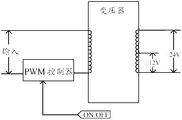
- the different windings of the same transformer in Figure 1 output +12V and +24V respectively.
- the same transformer outputs +24V to the same winding and draws +12V from the center.
- the external input switch motor signal ON/OFF controls the PWM controller to start, converting the rectified DC (ie, the inputs in Figures 1, 2) through the transformer to a +12V voltage and a +24V voltage output.
- OLED based displays have a faster response speed than other display schemes.
- the +12V voltage is consistent with the +24V voltage when switching on and off, as shown in Figure 3.
- the conversion of +12V voltage and +24V voltage will be turned on or off at the same time.
- the +12V voltage, +24V voltage and the on/off signal ON/OFF rise simultaneously (phase When it is turned on); at time T2, the +12V voltage, +24V voltage and the on/off signal ON/OFF decrease simultaneously (equivalent to turn off).
- the impact of the fast response characteristics of OLEDs can lead to unpredictable faults such as flower screens, so traditional power solutions are difficult to meet the requirements of OLEDs.
- an object of the present invention is to provide an OLED driving power supply device, which solves the problem that when the OLED display is used, the existing power supply architecture sharing transformer causes the output to be unstable, and the switching machine timing is simultaneously broken to cause the flower screen. problem.
- An OLED driving power supply device includes a power board connected to a main board and an OLED screen, wherein the power board includes: a standby circuit, a timing control module, a first conversion module, a second conversion module, and a PFC circuit;
- the standby circuit is configured to supply power to the main board and the timing control module after the power is turned on; the timing control module starts the PFC circuit according to the switch signal fed back by the main board, and the PFC circuit outputs the high voltage direct current to the timing control module, the first conversion module, and a second conversion module; the timing control module starts the first conversion module and the second conversion module according to the high voltage direct current and the enable signal outputted by the PFC circuit, and the first conversion module converts the high voltage direct current into the first voltage to supply power to the main board, and the second conversion module
- the method is used for converting the high voltage direct current into the second voltage to supply power to the main board and the OLED screen; the timing control module also controls the start timing of the first conversion module and the second conversion module, so that the switch signal and the enable signal are simultaneously stabilized and then the OLED is turned on. Screen.
- the timing control module includes:
- the switch timing control circuit is configured to output a first power source to start the PFC circuit according to the switch signal fed back by the main board, and supply the second power source according to the high voltage direct current output of the PFC circuit to the enable control circuit and the first conversion module;
- the control circuit is configured to output a third power supply to the second conversion module according to the enable signal fed back by the main board;
- the switch timing control circuit is connected to the PFC circuit, the enable control circuit, the first conversion module and the main board, and the enable control circuit is connected to the second conversion module.
- the first conversion module includes:
- a first PWM controller configured to start the first transformer according to the second power output of the switching timing control circuit
- a first transformer configured to convert a high voltage direct current outputted by the PFC circuit into a first voltage, and output the power to the main board;
- the first transformer is connected to the first PWM controller and the main board, and the first PWM controller is connected to the timing control module.
- the second conversion module includes:
- a second PWM controller configured to start the second transformer according to the third power output of the enable control circuit
- a second transformer configured to convert the high voltage direct current outputted by the PFC circuit into a second voltage, and output the power to the main board;
- the second transformer is connected to the second PWM controller and the main board, and the second PWM controller is connected to the timing control module.
- the standby circuit is also used to turn on the power
- the output operating voltage is output to the switch timing control circuit;
- the switch timing control circuit includes:
- a first power control sub-circuit configured to convert the operating voltage outputted by the standby circuit to the first power source according to the switch signal fed back by the main board to start the PFC circuit;
- a second power control sub-circuit configured to convert the working voltage into a second power supply according to the high-voltage direct current output after the PFC circuit is started, to supply power to the enable control circuit and the first conversion module;
- the first power control sub-circuit is connected to the standby circuit, the main board, the PFC circuit and the second power control sub-circuit, and the second power control sub-circuit is connected to the PFC circuit, the enable control circuit and the first conversion module.
- the first power control sub-circuit includes: a first triode, a second triode, a third triode, a first optocoupler, a first resistor, a second resistor, a third resistor, a fourth resistor, a first diode and a second diode; a base of the first transistor is connected to the main board, an emitter of the first transistor is grounded, and a set of the first triode
- the electrode is connected to the second leg of the first optocoupler, the first leg of the first optocoupler is connected to the standby circuit, and the fourth leg of the first optocoupler is connected to the collector of the standby circuit and the second triode, the first optocoupler
- the third leg is connected to one end of the first resistor, and the other end of the first resistor is connected to the base of the second transistor, the cathode of the first diode, and is also grounded through the second resistor, the first diode
- the anode of the tube is grounded, the emitting of
- the second power control sub-circuit includes: a fourth triode, a shunt reference source, and a voltage dividing resistor group; a base of the fourth triode is connected to a cathode of the shunt reference source, and a collector connection enable control circuit of the fourth triode And a control pole of the shunt reference source, the emitter of the fourth triode is connected to the first power control sub-circuit, the anode of the shunt reference source is grounded, the first end of the voltage dividing resistor group is connected to the PFC circuit, and the voltage dividing resistor The second end of the group is connected to the control pole of the shunt reference source, and the third end of the voltage dividing resistor group is grounded.
- the first power control sub-circuit further includes a third diode, a fifth resistor, a sixth resistor, a first capacitor, and a seventh resistor; and a positive pole of the third diode Connecting the main board, the negative pole of the third diode is connected to one end of the fifth resistor, the other end of the fifth resistor is connected to the base of the first triode, and is also grounded through a sixth resistor, and the first capacitor is connected in parallel with the sixth resistor
- the seventh resistor is connected between the standby circuit and the first leg of the first photocoupler.
- the second power control sub-circuit further includes an eighth resistor and a ninth resistor; one end of the eighth resistor is connected to the emitter of the fourth transistor, and the other end of the eighth resistor Connect the negative pole of the shunt reference source to one end of the ninth resistor, and the other end of the ninth resistor to the base of the fourth triode.
- the second power control sub-circuit further includes a fourth diode, a tenth resistor, a fifth diode, and a fourth capacitor; and a negative connection of the fourth diode is
- the control circuit and the first conversion module are connected, the anode of the fourth diode is connected to the collector of the fourth transistor, the anode of the fifth diode is also connected through the tenth resistor, and the cathode of the fifth diode is connected to the shunt reference.
- the control pole of the source, the fourth capacitor is connected between the control pole of the shunt reference source and the ground.
- the second power control sub-circuit further includes a fifth capacitor, an eleventh resistor, and a sixth diode; and the fifth capacitor is connected to the second end of the voltage dividing resistor group, The negative pole of the six diode is connected to the control pole of the shunt reference source, and the anode of the sixth diode is connected to the second end of the voltage dividing resistor group through the eleventh resistor.
- the enabling control circuit includes a fifth triode, a sixth triode, a second optocoupler, a twelfth resistor, a thirteenth resistor, and a seventh diode;
- the base of the fifth triode is connected to the main board, the emitter of the fifth triode is grounded, the collector of the fifth triode is connected to the second leg of the second optocoupler, and the first leg of the second optocoupler Connecting the standby circuit, the fourth pin of the second optocoupler is connected to the collector of the second power control sub-circuit and the sixth transistor, and the third leg of the second optocoupler is connected to one end of the twelfth resistor, the twelfth The other end of the resistor is connected to the base of the sixth triode, the cathode of the seventh diode, and is also grounded through the thirteenth resistor, the anode of the seventh diode is grounded, and the sixth transistor is emitted.
- the pole is connected to the second
- the OLED driving power supply device converts high voltage direct current into a first voltage to supply power to the main board through the first conversion module, and converts the high voltage direct current into a second voltage through the second conversion module to the main board and the OLED.
- the screen power supply makes the first voltage and the second voltage independent of each other, avoids the situation that the existing power supply architecture shares the transformer and causes the mutual interference and influence of the lines, satisfies the requirements of the OLED on the output stability of the power supply, and improves the image quality effect of the OLED;
- the timing control module controls the startup timing of the first conversion module and the second conversion module, so that the switch signal and the enable signal are simultaneously stabilized, then the OLED screen is illuminated, and the switching timing of the conventional power supply is changed, so that the power supply can adapt.
- the OLED fast response feature solves the problem that the existing switch timing is turned on or off at the same time. The problem.
- FIG. 1 is a schematic diagram showing output voltages of different windings of the same transformer in a conventional power supply architecture
- FIG. 2 is a schematic diagram of the output voltage of the same winding of the same transformer in the existing power supply architecture
- FIG. 3 is a timing diagram of a power switch in an existing power supply architecture
- FIG. 4 is a schematic diagram of an application embodiment of an OLED driving power supply device according to an embodiment of the present invention.
- FIG. 5 is a structural block diagram of a preferred embodiment of a power board according to an embodiment of the present invention.
- FIG. 6 is a schematic diagram of a pin of a socket connected between a power board and a main board according to an embodiment of the present invention
- FIG. 7 is a schematic diagram of a pin of a socket connected between a power board and an OLED screen according to an embodiment of the present invention.
- FIG. 8 is a circuit diagram of a switch timing control circuit according to an embodiment of the present invention.
- FIG. 9 is a circuit diagram of an enable control circuit according to an embodiment of the present invention.
- FIG. 10 is a timing diagram of a switch of an OLED driving power supply device according to an embodiment of the present invention.
- the present invention provides an OLED driving power supply device.
- the present invention will be further described in detail below with reference to the accompanying drawings and embodiments. It is understood that the specific embodiments described herein are merely illustrative of the invention and are not intended to limit the invention.
- the OLED driving power supply device provided by the invention is suitable for a power supply driving in a display field such as a television, a monitor, an audio-visual, a rear projection, a plasma display or the like using an OLED (Organic Light Emitting Diode) as a display scheme.
- the OLED driving power supply device provided by the present invention includes a power board 10 connected to the main board 20 and the OLED panel 30.
- the power board 10 includes a standby circuit 110, a timing control module 120, a first conversion module 130, a second conversion module 140, and a PFC circuit 150.
- the standby circuit 110 is connected to the timing control module 120 and the main board 20.
- the power supply voltage (5V in this embodiment) is outputted to the CPU of the main board 20 and the timing control module 120 to supply power to the CPU.
- the timing control module 120 is connected to the PFC circuit 150, the main board 20, the first conversion module 130, and the second conversion module 140.
- the timing control module 120 starts the PFC circuit 150 according to the ON/OFF of the power-on/off signal fed back by the CPU.
- the high voltage DC HV_DC is output to the timing control module, the first conversion module, and the second conversion module.
- the timing control module 120 activates the first conversion module 130 and the second conversion module 130 according to the high voltage DC HV_DC and the enable signal ENA, and controls the startup timing of the first conversion module 130 and the second conversion module 140 to turn the switch signal ON/OFF.
- the OLED screen is illuminated after the enable signal ENA is stabilized at the same time.
- the first conversion module 130 and the second conversion module 140 are connected to the main board 20 and the PFC circuit 150. After the first conversion module 130 is started, the high voltage direct current HV_DC is converted into a first voltage (in this embodiment, a voltage of +12V). The motherboard 20 is powered. After the second conversion module 140 is started, the high voltage direct current HV_DC is converted into a second voltage (+20V in this embodiment) to supply power to the main board 20 and the OLED panel 30.
- the timing control module 120 includes a switch timing control circuit 121 and an enable control circuit 122.
- the switch timing control circuit 121 is connected to the PFC circuit 150, the enable control circuit 122, the first conversion module 130, and the main board 20.
- the enable control circuit 122 is connected to the second conversion module 140.
- the switch timing control circuit 121 activates the PFC circuit 150 according to the switch power signal ON/OFF outputted by the main board, and outputs the second power source VCC1 to the enable control circuit 122 and the first conversion module according to the high voltage DC HV_DC outputted by the PFC circuit 150. 130 power supply.
- the enable control circuit 122 outputs the third power supply 20V_VCC to the second conversion module 140 according to the enable signal ENA fed back from the main board.
- the standby circuit further outputs an operating voltage (about 25V) to the switch timing control circuit after the power is turned on to provide a conversion power of the first power source PFC_VCC and the second power source VCC1.
- the switch timing control circuit specifically includes: a first power control sub-circuit 1211 and a second power control sub-circuit 1212.
- the first power control sub-circuit 1211 is connected to the standby circuit 110, the main board, the PFC circuit 150, and the second power control sub-circuit 1212.
- the second power control sub-circuit 1212 is connected to the PFC circuit 150, the enable control circuit 122, and the first Conversion module 1211.
- the first power control sub-circuit 1211 converts the operating voltage VCC output by the standby circuit 110 into the first power source PFC_VCC according to the switch signal fed back from the main board to activate the PFC circuit 150.
- the second power control sub-circuit 1212 is output after being activated according to the PFC circuit 150.
- the high voltage DC HV_DC converts the operating voltage VCC into a second power source VCC1 to supply power to the enable control circuit and the first conversion module.
- the embodiment uses an independent transformer and an independent PWM controller to convert the high voltage direct current into an independent +12V voltage and a +20V voltage output.
- the first conversion module 130 includes a first PWM controller 131 and a first transformer 132
- the second conversion module 140 includes a second PWM controller 141 and a second transformer 142.
- the first PWM controller 131 is connected to the timing control module, and activates the first transformer 132 according to the second power source VCC1 outputted by the switch timing control circuit; the first transformer 132 is connected to the first PWM controller 131 and the main board, which outputs the PFC circuit.
- the high voltage DC HV_DC is converted into a first voltage (ie, +12V), and the output is supplied to the motherboard.
- the second PWM controller 141 is connected to the timing control module, which activates the second transformer 142 according to the third power source 20V_VCC outputted by the enable control circuit; the second transformer 142 is connected to the second PWM controller and the main board, which will connect the PFC circuit
- the output high-voltage DC HV_DC is converted into a second voltage (ie, +20V), and the output is supplied to the main board.
- an independent transformer is used to respectively output a first voltage (ie, +12V) and a second voltage (ie, +20V) for power supply.
- the +12V and +20V are independent from each other at the root, and the two outputs and the PWM control are independent. Normal operation does not affect each other, thus avoiding interference between the two voltages.
- the output of the two voltages is completely separated, when the single load changes, the voltage output of the other circuit is not affected, thereby further ensuring the stability of the normal operation of the system.
- the organic film itself is driven by current to emit light, and the change of current causes the color of the picture. The change.
- the output of the first voltage and the second voltage on the power board are independent of each other, so that the whole machine is stable and normal during operation, effectively improving the electrical performance of the product, improving the image quality experience of the OLED TV, and delaying the use of the OLED screen. life.
- the standby circuit 110, the PFC circuit 150, the first PWM controller 131, and the second PWM controller 141 are all prior art, and the specific circuit structure thereof will not be described in detail herein.
- the display part of the TV set in actual application is composed of a power board, a main board, a TO-CON board, and a sub board (the constant current board is also included in the LED TV).
- the voltage and current required for the normal operation of these boards are provided by the power board.
- Different boards have different functions and different power requirements.
- Power consumption of the power board, main board, and screen body varies according to the size. Taking a 55-inch OLED TV as an example, the voltage supplied by the power board to the motherboard is +5V, +12V, and +20V, and the power board is directed to the OLED screen.
- the body provides a voltage of +20V and a maximum current of about 10A.
- a matching first socket is disposed on the power board 10 and the main board 20, and is connected to the first socket through a USB data line for connection.
- the first socket pin is as shown in FIG. 6. 4 and FIG. 6, it can be concluded that the data exchanged between the power board 10 and the main board 20 includes: an enable signal ENA, a switch signal ON/OFF, a 5V power supply voltage, a +12V first voltage, and a +20V. The second voltage and ground GND.
- the power board 10 and the OLED screen 30 are also respectively provided with a matching second socket, which is inserted into the second socket through the USB data line for connection.
- the second socket pin is as shown in FIG. 7. Referring to FIG. 4 and FIG.
- the data exchanged between the power board 10 and the OLED screen includes: a second voltage of +20V and a ground GND.
- the OLED screen is illuminated by a second voltage of +20V.
- the main board 20 and the OLED screen are also connected through a socket and a USB data line.
- the main board 20 transmits a first voltage of +12 V to supply power to the relevant control circuit of the OLED screen, and controls the content display of the OLED screen through the data Data.
- the socket pins can be appropriately increased or decreased, which is subject to the actual voltage requirements.
- the power-on/off timing of the power supply is also adjusted by the power-on/off signal and the enable signal ENA fed back by the CPU on the main board.
- the OLED screen is illuminated only when the switch signal ON/OFF and the enable signal ENA are simultaneously turned on, so that the OLED driving power supply device provided by the embodiment can meet the timing requirements of the OLED screen.
- the switch timing is adjusted by the switch timing control circuit and the enable control circuit.
- the first power control sub-circuit 1211 includes: a first transistor Q1, a second transistor Q2, a third transistor Q3, and a first photocoupler U1.
- the first power control sub-circuit 1212 includes a fourth transistor Q4, a shunt reference source T, and a voltage dividing resistor group 1210.
- the base of the first transistor Q1 is connected to the main board (for inputting the switch signal ON/OFF), the emitter of the first transistor Q1 is grounded, and the collector of the first transistor Q1 is connected to the first optocoupler
- the second leg of U1 ie, the negative pole of the LED
- the first leg of the first optocoupler U1 ie, the anode of the LED
- the fourth leg ie, the collector of the phototransistor
- the third leg of the first photocoupler U1 ie, the emitter of the phototransistor
- the other end of the first resistor R1 is connected to the base of the second transistor Q2, the cathode of the first diode D1, and is also open
- the second resistor R2 is grounded, the anode of the first diode D1 is grounded, the emitter of the second transistor Q2 is connected to the collector of the third transistor Q3, one end of the third resistor R3, and the fourth The emitter of the transistor Q4, the other end of the third resistor R3 is connected to the base of the third transistor Q3, the cathode of the second diode D2, and is also grounded through the fourth resistor R4, the second two
- the anode of the pole tube D2 is grounded, the emitter of the third transistor Q3 is connected to the PFC circuit (for outputting the first power source PFC_VCC), and the base of the fourth transistor Q4 is connected to the cathode K of the shunt reference source T,
- the collector of the four transistor Q4 is connected to the control circuit, the first conversion module, and the control electrode VRE of the
- the first transistor Q1, the second transistor Q2, and the third transistor Q3 are all NPN transistors, and the fourth transistor Q4 is a PNP transistor.
- the first diode D1 and the second diode D2 are Zener diodes that can protect the second transistor Q2 and the third transistor Q3.
- the shunt reference source T is of the type TL431 and has a turn-on voltage of 2.5V.
- the model of the first photocoupler U1 is PC817.
- the voltage dividing resistor group 1210 is composed of a plurality of series resistors.
- the first voltage dividing resistor Ra, the second voltage dividing resistor Rb, the third voltage dividing resistor Rc, and the fourth voltage dividing resistor Rd are sequentially connected in series.
- the fifth voltage dividing resistor Re is sequentially connected in series.
- One end of the first voltage dividing resistor Ra (corresponding to the first end of the voltage dividing resistor group 1210) is connected to a PFC circuit for inputting a high voltage DC HV_DC, and one end of the fifth voltage dividing resistor Re (corresponding to the voltage dividing resistor group 1210) Third
- the connection point of the fourth voltage dividing resistor Rd and the fifth voltage dividing resistor Re (corresponding to the second end of the voltage dividing resistor group 1210) is connected to the control electrode VRE of the shunt reference source T.
- the first power control sub-circuit 1211 further includes a filter voltage dividing circuit composed of a third diode D3, a fifth resistor R5, a sixth resistor R6, and a first capacitor C1, and a current limiting circuit.
- the seventh resistor R7 The anode of the third diode D3 is connected to the main board, the cathode of the third diode D3 is connected to one end of the fifth resistor R5, and the other end of the fifth resistor R5 is connected to the base of the first transistor Q1.
- the sixth resistor R6 is grounded, and the first capacitor C1 is connected in parallel with the sixth resistor R6.
- the partial voltage of the fifth resistor R5 and the sixth resistor R6 is the turn-on voltage at the base of the first transistor Q1, which determines the conduction state of the first transistor Q1, and the first capacitor C1 is opposite to the guide.
- the pass voltage is smoothed and filtered to improve the stability of the on state.
- the seventh resistor R7 is connected between the standby circuit and the first leg of the first photocoupler U1.
- the switch timing control circuit further includes two polar capacitors, that is, a second capacitor C2 and a third capacitor C3, and the anode of the second capacitor C2 is connected to the second transistor Q2.
- the emitter, the cathode of the second capacitor C2 is grounded; the anode of the third capacitor is connected to the emitter of the third transistor Q3, and the cathode of the third capacitor C3 is grounded.
- the second power control sub-circuit 1212 further includes an eighth resistor R8 and a ninth resistor R9 for setting a bias voltage and adjusting an on state of the fourth transistor Q4.
- One end of the eighth resistor R8 is connected to the emitter of the fourth transistor Q4, and the eighth power
- the other end of the resistor R8 is connected to one end of the negative electrode K of the shunt reference source T and the ninth resistor R9, and the other end of the ninth resistor R9 is connected to the base of the fourth transistor Q4.
- the group value of the eighth resistor R8 and the ninth resistor R9 determines the voltage value of the second power source VCC1.
- the second power control sub-circuit 1212 further includes a fourth diode D4 for blocking and filtering, for performing the feedback control to divide the reference source T continuously.
- the cathode of the fourth diode D4 is connected to the enable control circuit and the first conversion module, and the anode of the fourth diode D4 is connected to the collector of the fourth transistor Q4, and is also connected through the tenth resistor R10.
- the anode of the pole D5, the cathode of the fifth diode D5 is connected to the gate VRE of the shunt reference source T, and the fourth capacitor C4 is connected between the gate VRE of the shunt reference source T and the ground.
- the second power control sub-circuit 1212 further includes a fifth capacitor C5 for filtering, an eleventh resistor R11 for current limiting, and a sixth for alternating current. Diode D6.
- the fifth capacitor C5 is connected to the second end of the voltage dividing resistor group (ie, in parallel with the fifth voltage dividing resistor Re), and the cathode of the sixth diode D6 is connected to the control electrode VRE of the shunt reference source T, the sixth diode
- the positive electrode of D6 is connected to the second end of the voltage dividing resistor group 1210 through the eleventh resistor R11.
- the enable control circuit includes a fifth transistor Q5, a sixth transistor Q6, a second photocoupler U2, a twelfth resistor R12, a thirteenth resistor R13, and a seventh diode. D7; the base of the fifth transistor Q5 is connected to the main board (for input enable signal ENA), the emitter of the fifth transistor Q5 is grounded, and the collector of the fifth transistor Q5 is connected to the second optocoupler
- the second leg of U2 ie, the negative pole of the LED
- the first leg of the second photocoupler U2 ie, the positive pole of the LED
- the fourth pin of the second optocoupler U2 ie, the collector of the phototransistor
- the collector of the transistor Q6 the third leg of the second photocoupler U2 (ie, the emitter of the phototransistor) is connected to one end of the twelfth
- the fifth transistor Q5 and the sixth transistor Q6 are both NPN transistors.
- the seventh diode D7 is a Zener diode and can protect the sixth transistor Q6. Adjusting the resistance values of the twelfth resistor R12 and the thirteenth resistor R13 can affect the conduction state of the sixth transistor Q6, thereby controlling the voltage value of the third power source 20V_VCC.
- the enable control circuit further includes an eighth diode D8, a fourteenth resistor R14, a fifteenth resistor R15 and a sixth capacitor C6.
- the anode of the eighth diode D8 is connected to the main board (for input enable signal ENA), the cathode of the eighth diode D8 is connected to one end of the fourteenth resistor R14, and the other end of the fourteenth resistor R14 is connected to the fifth.
- the base of the transistor Q5 is also grounded through a fifteenth resistor R15, which is connected in parallel with the fifteenth resistor R15.
- the divided voltage of the fourteenth resistor R14 and the fifteenth resistor R15 is the turn-on voltage of the fifth transistor Q5, which determines the conduction state of the fifth transistor Q5, and the sixth capacitor C6 is turned on.
- the voltage is smoothed and filtered to improve the stability of the on state.
- the standby circuit 110 After the external power is externally connected to the OLED driving power supply device, the standby circuit 110 outputs a power supply voltage of +5 V to supply power to the CPU of the main board and the first leg of the first photocoupler U1. At the same time, the standby circuit 110 also outputs an operating voltage VCC (about 25 V) to supply power to the collectors of the fourth pin and the second transistor Q2 of the first photocoupler U1.
- VCC about 25 V
- the switch timing control circuit of the power board is provided with a switch signal ON/OFF (active high, equivalent to the start signal), so that the first transistor Q1 is saturated and turned on.
- the conduction amount of the first photocoupler U1 is increased, the phototransistor is turned on to increase the base voltage of the second transistor Q2, and the second transistor Q2 is turned on to make the base of the third transistor Q3 As the voltage rises, the third transistor Q3 is also saturated.
- the working voltage VCC is sequentially stepped down by the second transistor Q2 and the third transistor Q3, and then the first power source PFC_VCC is output to supply power to the PFC circuit.
- the PFC circuit of the power board starts to work, and a high voltage DC HV_DC (higher than 380V) is generated and fed back to the first end of the voltage dividing resistor group 1210.
- the high voltage DC HV_DC is divided by the voltage dividing resistor group 1210 to a voltage higher than 2.5V to the control pole VRE of the shunt reference source T, and the shunt reference source T is turned on to make the base of the fourth triode Q4 extremely low, fourth Transistor Q4 is turned on.
- the working voltage VCC is sequentially stepped down by the second transistor Q2 and the fourth transistor Q4, and then the second power source VCC1 is output to the first conversion module, and the first conversion module converts the second power source VCC1 into a first voltage of +12V.
- ENA active high, equivalent to the dot screen
- the enable control circuit of the power supply board receives the enable signal ENA
- the fifth transistor Q5 is turned on, the conduction amount of the second photocoupler U2 is increased, and the base voltage of the sixth transistor Q6 is increased.
- Transistor Q6 is saturated and conducting.
- the second power source VCC1 passes through the sixth triode
- the third power supply 20V_VCC is output to the second conversion module, and the second conversion module converts the third power supply 20V_VCC into a second voltage of +20V to supply power to the main board and the OLED panel.
- the OLED screen will be illuminated at this time.
- the motherboard also delivers a second voltage of +20V to the power amplifier circuit (this is a prior art and will not be described in detail herein).
- the first transistor Q1 When the switch signal ON/OFF is low (equivalent to the shutdown signal), the first transistor Q1 is turned off to turn off the first photocoupler U1, and the second transistor Q2 and the third transistor Q3 are turned off sequentially.
- the PFC circuit stops working, then no high voltage DC HV_DC is generated, the fourth transistor Q4 is also cut off, no second power supply VCC1 is output, and the first conversion module stops working, resulting in no first voltage output.
- the enable signal ENA When the enable signal ENA is at a low level (equivalent to a screen off), the fifth transistor Q5 is turned off to turn off the second photocoupler U2, and the sixth transistor Q6 is also turned off.
- the third power supply 20V_VCC becomes a low level, so that the second conversion module stops working, and the second voltage without +20V supplies power to the OLED screen, and the OLED screen is turned off.
- FIG. 1 A schematic diagram of the timing of the switching machine obtained after performing circuit simulation on the OLED driving power supply device is shown in FIG.
- the first conversion module 130 is controlled to output a first voltage of +12 V to the main board 20.
- the main board 20 starts to work, and after the T2 time, the main board 20 sends the data Data to the OLED screen 30. Since there is no second voltage of +20V at this time, the OLED screen is not lit yet.
- the main board 20 feeds back the enable signal ENA to the power board 10.
- the second converter module 140 is controlled to output a second voltage of +20V to the main board and the OLED screen. After the time of T4, the second voltage reaches a stable output, OLED The screen is lit and the data display screen is recognized. The voltage is turned on from +12V to +20V and is turned on for at least 36ms (T1+T2+T3+T4).
- the main board When the power is turned off, the main board sends a low level enable signal ENA (equivalent to the off signal) to the power board, the power board stops outputting the second voltage of +20V, and the OLED screen is turned off.
- ENA low level enable signal
- the main board 20 emits a low-level switch signal ON/OFF (low level is equivalent to the shutdown signal), and the power board stops outputting the first voltage of +12V, and the whole machine enters the standby state.
- the T6 time is not less than 30 ms. In this way, the OLED screen and the motherboard are not simultaneously turned on, and the problem of the flower screen is avoided.
- the OLED driving power supply device provided by the present invention, after the AC power supply is connected, firstly outputs a 5V power supply voltage to the CPU of the main board by the standby circuit of the power supply board, and the feedback switch machine signal is turned ON/OFF after the CPU works normally.
- the switching timing control circuit of the power board outputs the first power source PFC_VCC to start the PFC circuit, and the high voltage DC outputted by the PFC circuit causes the switching timing control circuit to output the second power source VCC1 to perform the +12V voltage conversion to the first conversion module, and simultaneously to enable the control circuit.
- Power supply after the power board outputs +12V voltage to the motherboard, the main board then feedbacks the enable signal ENA to the enable control circuit, so that it outputs the third power supply 20V_VCC to the second conversion module for +20V voltage conversion, and the power board outputs +20V voltage point.
- the enable signal ENA to the enable control circuit
- the two voltage outputs and the control are independent of each other, and do not affect each other, thereby avoiding the prior art sharing.
- the transformer causes interference between the two voltages.
- the output of the two voltages is completely separated, when the single load changes, the voltage output of the other circuit is not affected, so that the whole machine is stable and normal during operation. Effectively improve the electrical performance of the product, improve the image quality experience of OLED TV, and delay the service life of OLED screen.
- the invention outputs the +20V voltage to simultaneously illuminate the OLED screen after the shutdown signal and the enable signal are simultaneously stabilized, and changes the timing of the switching of the conventional power supply, so that the power supply can adapt to the fast response characteristics of the OLED, and solves the existing switching sequence.
- the break causes the problem of the flower screen.
Landscapes
- Engineering & Computer Science (AREA)
- Physics & Mathematics (AREA)
- Computer Hardware Design (AREA)
- General Physics & Mathematics (AREA)
- Theoretical Computer Science (AREA)
- Power Engineering (AREA)
- Electroluminescent Light Sources (AREA)
Abstract
Description
Claims (14)
- 一种OLED驱动电源装置,包括与主板和OLED屏连接的电源板,其特征在于,所述电源板包括:待机电路、时序控制模块、第一转换模块、第二转换模块和PFC电路;所述待机电路用于接通电源后输出电源电压给主板和时序控制模块供电;时序控制模块根据主板反馈的开关机信号启动PFC电路;PFC电路输出高压直流给时序控制模块、第一转换模块和第二转换模块;时序控制模块根据PFC电路输出的高压直流、使能信号启动第一转换模块和第二转换模块,第一转换模块将高压直流转换成第一电压给主板供电,第二转换模块将高压直流转换成第二电压给主板和OLED屏供电;时序控制模块还控制第一转换模块和第二转换模块的启动时序,使开关机信号和使能信号同时稳定后点亮OLED屏。
- 根据权利要求1所述的OLED驱动电源装置,其特征在于,所述第一转换模块包括:第一PWM控制器,用于根据开关时序控制电路输出的第二电源启动第一变压器;第一变压器,用于将PFC电路输出的高压直流转换成第一电压、输出给主板供电;所述第一变压器连接第一PWM控制器和主板,所述第一PWM控制器连接时序控制模块。
- 根据权利要求1所述的OLED驱动电源装置,其特征在于,所述第二转换模块包括:第二PWM控制器,用于根据使能控制电路输出的第三电源启动第二变压器;第二变压器,用于将PFC电路输出的高压直流转换成第二电压、输出给主板供电;第二变压器连接第二PWM控制器和主板,所述第二PWM控制器连接时序控制模块。
- 一种OLED驱动电源装置,包括与主板和OLED屏连接的电源板,其特征在于,所述电源板包括:待机电路、时序控制模块、第一转换模块、第二转换模块和PFC电路;所述待机电路用于接通电源后输出电源电压给主板和时序控制模块供电;时序控制模块根据主板反馈的开关机信号启动PFC电路;PFC电路输出高压直流给时序控制模块、第一转换模块和第二转换模块;时序控制模块根据PFC电路输出的高压直流、使能信号启动第一转换模块和第二转换模块,第一转换模块将高压直流转换成第一电压给主板供电,第二转换模块将高压直流转换成第二电压给主板和OLED屏供电;时序控制模块还控制第一转换模块和第二转换模块的启动时序,使开关机信号和使能信号同时稳定后点亮OLED屏,所述时序控制模块包括:开关时序控制电路,用于根据主板反馈的开关机信号输出第一电源启动PFC电路,根据PFC电路输出的高压直流输出第二电源给使能控制电路和第一转换模块供电;使能控制电路,用于根据主板反馈的使能信号输出第三电源给第 二转换模块供电;所述开关时序控制电路连接PFC电路、使能控制电路、第一转换模块和主板,所述使能控制电路连接第二转换模块。
- 根据权利要求4所述的OLED驱动电源装置,其特征在于,所述第一转换模块包括:第一PWM控制器,用于根据开关时序控制电路输出的第二电源启动第一变压器;第一变压器,用于将PFC电路输出的高压直流转换成第一电压、输出给主板供电;所述第一变压器连接第一PWM控制器和主板,所述第一PWM控制器连接时序控制模块。
- 根据权利要求4所述的OLED驱动电源装置,其特征在于,所述第二转换模块包括:第二PWM控制器,用于根据使能控制电路输出的第三电源启动第二变压器;第二变压器,用于将PFC电路输出的高压直流转换成第二电压、输出给主板供电;第二变压器连接第二PWM控制器和主板,所述第二PWM控制器连接时序控制模块。
- 根据权利要求4所述的OLED驱动电源装置,其特征在于,所述待机电路还用于接通电源后输出工作电压给开关时序控制电路;所述开关时序控制电路包括:第一电源控制子电路,用于根据主板反馈的开关机信号将待机电路输出的工作电压转换为第一电源来启动PFC电路;第二电源控制子电路,用于根据PFC电路启动后输出的高压直流将所述工作电压转换为第二电源给使能控制电路和第一转换模块供电;所述第一电源控制子电路连接待机电路、主板、PFC电路和第二电源控制子电路,所述第二电源控制子电路连接PFC电路、使能控制电路和第一转换模块。
- 根据权利要求4所述的OLED驱动电源装置,其特征在于,所述第一电源控制子电路包括:第一三极管、第二三极管、第三三极管、第一光耦、第一电阻、第二电阻、第三电阻、第四电阻、第一二极管和第二二极管;所述第一三极管的基极连接主板,第一三极管的发射极接地,第一三极管的集电极连接第一光耦的第2脚,所述第一光耦的第1脚连接待机电路,第一光耦的第4脚连接待机电路和第二三极管的集电极,第一光耦的第3脚连接第一电阻的一端,所述第一电阻的另一端连接第二三极管的基极、第一二极管的负极、还通过第二电阻接地,所述第一二极管的正极接地,所述第二三极管的发射极连接第三三极管的集电极、第三电阻的一端和第二电源控制子电路,所述第三电阻的另一端连接第三三极管的基极、第二二极管的负极、还通过第四电阻接地,所述第二二极管的正极接地,第三三极管的发射极连接PFC电路。
- 根据权利要求4所述的OLED驱动电源装置,其特征在于, 所述第二电源控制子电路包括:第四三极管、分流基准源和分压电阻组;所述第四三极管的基极连接分流基准源的负极,第四三极管的集电极连接使能控制电路、第一转换模块和分流基准源的控制极,第四三极管的发射极连接第一电源控制子电路,所述分流基准源的正极接地,所述分压电阻组的第一端连接PFC电路,分压电阻组的第二端连接分流基准源的控制极,分压电阻组的第三端接地。
- 根据权利要求8所述的OLED驱动电源装置,其特征在于,所述第一电源控制子电路还包括第三二极管、第五电阻、第六电阻、第一电容和第七电阻;所述第三二极管的正极连接主板,第三二极管的负极连接第五电阻的一端,第五电阻的另一端连接第一三极管的基极、还通过第六电阻接地,所述第一电容与第六电阻并联,所述第七电阻连接在待机电路与第一光耦的第1脚之间。
- 根据权利要求9所述的OLED驱动电源装置,其特征在于,所述第二电源控制子电路还包括第八电阻和第九电阻;所述第八电阻的一端连接第四三极管的发射极,第八电阻的另一端连接分流基准源的负极与第九电阻的一端,第九电阻的另一端连接第四三极管的基极。
- 根据权利要求9所述的OLED驱动电源装置,其特征在于,所述第二电源控制子电路还包括第四二极管、第十电阻、第五二极管和第四电容;所述第四二极管的负极连接使能控制电路和第一转换模块,第四二极管的正极连接第四三极管的集电极、还通过第十电阻连接第五二极管的正极,第五二极管的负极连接分流基准源的控制极,第四电容连接在分流基准源的控制极与地之间。
- 根据权利要求9所述的OLED驱动电源装置,其特征在于,所述第二电源控制子电路还包括第五电容、第十一电阻和第六二极管;所述第五电容连接分压电阻组的第2端,第六二极管的负极连接分流基准源的控制极,第六二极管的正极通过第十一电阻连接分压电阻组的第2端。
- 根据权利要求9所述的OLED驱动电源装置,其特征在于,所述使能控制电路包括第五三极管、第六三极管、第二光耦、第十二电阻、第十三电阻和第七二极管;所述第五三极管的基极连接主板,第五三极管的发射极接地,第五三极管的集电极连接第二光耦的第2脚,所述第二光耦的第1脚连接待机电路,第二光耦的第4脚连接第二电源控制子电路和第六三极管的集电极,第二光耦的第3脚连接第十二电阻的一端,所述第十二电阻的另一端连接第六三极管的基极、第七二极管的负极、还通过第十三电阻接地,所述第七二极管的正极接地,所述第六三极管的发射极连接第二转换模块。
Priority Applications (2)
| Application Number | Priority Date | Filing Date | Title |
|---|---|---|---|
| US14/770,051 US9603219B2 (en) | 2014-03-18 | 2014-09-22 | Driving power supply apparatus for OLED |
| AU2014379985A AU2014379985B2 (en) | 2014-03-18 | 2014-09-22 | A driving power supply apparatus for OLED |
Applications Claiming Priority (2)
| Application Number | Priority Date | Filing Date | Title |
|---|---|---|---|
| CN201410099656.3 | 2014-03-18 | ||
| CN201410099656.3A CN103889118B (zh) | 2014-03-18 | 2014-03-18 | 一种oled驱动电源装置 |
Publications (1)
| Publication Number | Publication Date |
|---|---|
| WO2015139437A1 true WO2015139437A1 (zh) | 2015-09-24 |
Family
ID=50957781
Family Applications (1)
| Application Number | Title | Priority Date | Filing Date |
|---|---|---|---|
| PCT/CN2014/087027 Ceased WO2015139437A1 (zh) | 2014-03-18 | 2014-09-22 | 一种oled驱动电源装置 |
Country Status (4)
| Country | Link |
|---|---|
| US (1) | US9603219B2 (zh) |
| CN (1) | CN103889118B (zh) |
| AU (1) | AU2014379985B2 (zh) |
| WO (1) | WO2015139437A1 (zh) |
Cited By (2)
| Publication number | Priority date | Publication date | Assignee | Title |
|---|---|---|---|---|
| CN106026714A (zh) * | 2016-07-29 | 2016-10-12 | 合肥工业大学 | 一种单级双极性增益隔离型变换器 |
| WO2023280011A1 (zh) * | 2021-07-05 | 2023-01-12 | 南京中车浦镇海泰制动设备有限公司 | 一种基于频率控制的高可靠性休眠电路 |
Families Citing this family (37)
| Publication number | Priority date | Publication date | Assignee | Title |
|---|---|---|---|---|
| CN103889118B (zh) * | 2014-03-18 | 2016-02-10 | 深圳创维-Rgb电子有限公司 | 一种oled驱动电源装置 |
| KR102215086B1 (ko) * | 2014-09-16 | 2021-02-15 | 삼성디스플레이 주식회사 | 전압 공급 회로 및 이를 포함하는 디스플레이 장치 |
| CN105356741B (zh) * | 2015-12-07 | 2019-02-05 | 一巨自动化装备(上海)有限公司 | 一种电动汽车DCDC Converter的使能信号控制电路 |
| CN106488607B (zh) * | 2016-09-09 | 2018-04-10 | 深圳创维-Rgb电子有限公司 | 开关电源及电视机 |
| CN106448586B (zh) * | 2016-09-27 | 2019-06-28 | 青岛海信电器股份有限公司 | 液晶装置及液晶屏的电源供给的开关控制方法 |
| CN106409220B (zh) * | 2016-09-29 | 2019-01-29 | 深圳创维-Rgb电子有限公司 | 一种oled驱动电源装置及oled电视 |
| JP6851179B2 (ja) | 2016-11-07 | 2021-03-31 | キヤノン株式会社 | 電源装置とその制御方法 |
| CN108462389A (zh) * | 2017-02-21 | 2018-08-28 | 辽宁壮龙无人机科技有限公司 | 电源管理电路和应用该电路的电源管理模块以及无人机 |
| KR102420998B1 (ko) * | 2017-08-04 | 2022-07-13 | 엘지디스플레이 주식회사 | 통신 방법과 이를 이용한 표시장치 |
| CN107464533B (zh) * | 2017-08-21 | 2019-10-11 | 深圳创维-Rgb电子有限公司 | 一种恒流驱动电路及电视机 |
| KR102398553B1 (ko) * | 2017-08-29 | 2022-05-17 | 엘지디스플레이 주식회사 | 유기발광 표시장치 |
| JP6702284B2 (ja) * | 2017-09-05 | 2020-06-03 | 株式会社デンソー | 液晶パネルの駆動回路および液晶表示装置 |
| CN109754748B (zh) * | 2017-11-03 | 2021-05-14 | 上海和辉光电股份有限公司 | 一种显示面板的驱动电路、显示面板及显示装置 |
| CN107889330A (zh) * | 2017-12-14 | 2018-04-06 | 宁波绿光能源科技有限公司 | 一种一体化太阳能路灯自激电路 |
| CN208257679U (zh) * | 2018-05-07 | 2018-12-18 | 江苏欧帝电子科技有限公司 | 一种驱动电源、触控黑板及其组合黑板 |
| CN109119021A (zh) | 2018-09-07 | 2019-01-01 | 深圳创维-Rgb电子有限公司 | 一种oled驱动电源及oled电视 |
| CN109166519A (zh) * | 2018-09-07 | 2019-01-08 | 深圳创维-Rgb电子有限公司 | 一种oled驱动电源和oled电视 |
| KR102673597B1 (ko) | 2018-09-12 | 2024-06-12 | 삼성전자주식회사 | 디스플레이 시스템, 디스플레이 장치 및 그 제어 방법 |
| US11200837B2 (en) | 2018-09-25 | 2021-12-14 | Hisense Visual Technology Co., Ltd. | OLED display device, and method for controlling the OLED display device |
| WO2020062905A1 (zh) * | 2018-09-25 | 2020-04-02 | 青岛海信电器股份有限公司 | 一种oled显示装置及其控制方法 |
| CN109347465B (zh) * | 2018-10-29 | 2022-09-16 | 阳光电源(上海)有限公司 | 开关管驱动电路、关断器和分布式发电系统 |
| CN111628627B (zh) * | 2019-02-28 | 2024-04-23 | 中国科学院沈阳自动化研究所 | 一种水下潜标可扩展电源系统 |
| KR102646067B1 (ko) | 2019-07-17 | 2024-03-12 | 삼성전자주식회사 | 전자 장치, 그 제어 방법 및 디스플레이 장치 |
| TWI731691B (zh) * | 2020-05-21 | 2021-06-21 | 緯創資通股份有限公司 | 發光二極體顯示系統及模組 |
| US11244622B2 (en) * | 2020-06-04 | 2022-02-08 | Parade Technologies, Ltd. | Dynamic power control for OLED displays |
| CN111681606B (zh) * | 2020-07-22 | 2021-11-19 | 宁波视睿迪光电有限公司 | 保护控制电源、oled屏幕控制系统和oled屏幕 |
| CN112290774A (zh) * | 2020-10-30 | 2021-01-29 | 深圳市创维群欣安防科技股份有限公司 | 一种基于单片机的待机控制电路及用电设备 |
| CN112511902B (zh) * | 2020-11-18 | 2022-08-02 | 深圳创维-Rgb电子有限公司 | Oled电视终端的显示屏控制方法、装置及oled电视终端 |
| CN112701906B (zh) * | 2020-12-11 | 2022-07-12 | Tcl华星光电技术有限公司 | 直流变压电路 |
| CN113593486B (zh) * | 2021-07-28 | 2022-11-04 | 深圳创维-Rgb电子有限公司 | 一种mini led驱动电源及mini led电视 |
| CN114999408B (zh) * | 2022-06-17 | 2025-04-25 | 深圳市华星光电半导体显示技术有限公司 | 开关控制电路以及背光驱动板 |
| CN114882840B (zh) * | 2022-06-18 | 2023-06-30 | 广东省魔丽显示科技有限公司 | 一种显示面板驱动电源电路 |
| CN115441693A (zh) * | 2022-09-09 | 2022-12-06 | 海信视像科技股份有限公司 | 显示装置 |
| CN115987095A (zh) * | 2023-01-04 | 2023-04-18 | 长沙湘计海盾科技有限公司 | 一种电源板及加固显示器的电源电路 |
| CN117037651A (zh) * | 2023-08-21 | 2023-11-10 | 京东方科技集团股份有限公司 | 显示模组、显示装置以及显示模组驱动方法 |
| KR20250104540A (ko) * | 2023-12-29 | 2025-07-08 | 엘지디스플레이 주식회사 | 전계 발광 표시장치 및 그 구동방법 |
| TWI902394B (zh) * | 2024-08-13 | 2025-10-21 | 台達電子工業股份有限公司 | 供電時序控制裝置及方法 |
Citations (4)
| Publication number | Priority date | Publication date | Assignee | Title |
|---|---|---|---|---|
| CN201563268U (zh) * | 2009-11-04 | 2010-08-25 | 河源市超越光电科技有限公司 | 用于oled灯具的驱动电路 |
| CN202102692U (zh) * | 2011-06-16 | 2012-01-04 | 青岛海信电器股份有限公司 | 一种led驱动电路及液晶电视机 |
| US20130169517A1 (en) * | 2011-12-28 | 2013-07-04 | Samsung Electronics Co., Ltd. | Power supplying apparatus, power supplying method, organic light-emitting diode display apparatus |
| CN103889118A (zh) * | 2014-03-18 | 2014-06-25 | 深圳创维-Rgb电子有限公司 | 一种oled驱动电源装置 |
Family Cites Families (17)
| Publication number | Priority date | Publication date | Assignee | Title |
|---|---|---|---|---|
| KR100229604B1 (ko) * | 1996-11-14 | 1999-11-15 | 윤종용 | 역률보정회로를 갖는 디스플레이 모니터 전원 공급 장치 |
| US7269034B2 (en) * | 1997-01-24 | 2007-09-11 | Synqor, Inc. | High efficiency power converter |
| JP3463675B2 (ja) * | 2001-06-29 | 2003-11-05 | ソニー株式会社 | スイッチング電源装置 |
| DE60302239T2 (de) * | 2003-07-22 | 2006-07-27 | Barco N.V. | Methode zur Steuerung einer Anzeige aus organischen Leuchtdioden und Anzeigevorrichtung, die zur Ausführung dieser Methode eingerichtet ist |
| KR101243402B1 (ko) * | 2005-12-27 | 2013-03-13 | 엘지디스플레이 주식회사 | 액정표시소자의 하이브리드 백라이트 구동 장치 |
| JP2007329996A (ja) * | 2006-06-06 | 2007-12-20 | Sharp Corp | スイッチング電源装置 |
| US8296587B2 (en) * | 2006-08-30 | 2012-10-23 | Green Plug, Inc. | Powering an electrical device through a legacy adapter capable of digital communication |
| US20080218503A1 (en) * | 2007-03-08 | 2008-09-11 | Il-Woon Lee | Power supply, plasma display including power supply, and method of driving plasma display |
| JP2011004473A (ja) * | 2009-06-16 | 2011-01-06 | Sanyo Electric Co Ltd | 電源回路および投写型表示装置 |
| WO2011026047A1 (en) * | 2009-08-28 | 2011-03-03 | Green Plug | High-and low-power power supply with standby power saving features |
| CN102405587A (zh) * | 2010-05-04 | 2012-04-04 | 华为技术有限公司 | Dc/dc变换器 |
| CN202008730U (zh) * | 2011-05-16 | 2011-10-12 | 北京浩天融智电气科技有限公司 | 一种带oled显示的智能开关装置 |
| CN102646388B (zh) * | 2011-06-02 | 2015-01-14 | 京东方科技集团股份有限公司 | 一种驱动装置、oled面板及oled面板驱动方法 |
| KR20130076413A (ko) * | 2011-12-28 | 2013-07-08 | 삼성전자주식회사 | 전원공급장치, 이를 구비한 디스플레이 장치 및 전원 공급 방법 |
| KR20130076293A (ko) * | 2011-12-28 | 2013-07-08 | 삼성전기주식회사 | 직류/직류 컨버터 및 이를 갖는 구동 장치 |
| GB2499220B (en) * | 2012-02-08 | 2018-12-12 | Radiant Res Limited | A power control system for an illumination system |
| US9354743B2 (en) * | 2014-04-16 | 2016-05-31 | Microchip Technology Incorporated | Apparatus for improving signal-to-noise performance of projected capacitance touch screens and panels |
-
2014
- 2014-03-18 CN CN201410099656.3A patent/CN103889118B/zh active Active
- 2014-09-22 WO PCT/CN2014/087027 patent/WO2015139437A1/zh not_active Ceased
- 2014-09-22 AU AU2014379985A patent/AU2014379985B2/en active Active
- 2014-09-22 US US14/770,051 patent/US9603219B2/en active Active
Patent Citations (4)
| Publication number | Priority date | Publication date | Assignee | Title |
|---|---|---|---|---|
| CN201563268U (zh) * | 2009-11-04 | 2010-08-25 | 河源市超越光电科技有限公司 | 用于oled灯具的驱动电路 |
| CN202102692U (zh) * | 2011-06-16 | 2012-01-04 | 青岛海信电器股份有限公司 | 一种led驱动电路及液晶电视机 |
| US20130169517A1 (en) * | 2011-12-28 | 2013-07-04 | Samsung Electronics Co., Ltd. | Power supplying apparatus, power supplying method, organic light-emitting diode display apparatus |
| CN103889118A (zh) * | 2014-03-18 | 2014-06-25 | 深圳创维-Rgb电子有限公司 | 一种oled驱动电源装置 |
Cited By (2)
| Publication number | Priority date | Publication date | Assignee | Title |
|---|---|---|---|---|
| CN106026714A (zh) * | 2016-07-29 | 2016-10-12 | 合肥工业大学 | 一种单级双极性增益隔离型变换器 |
| WO2023280011A1 (zh) * | 2021-07-05 | 2023-01-12 | 南京中车浦镇海泰制动设备有限公司 | 一种基于频率控制的高可靠性休眠电路 |
Also Published As
| Publication number | Publication date |
|---|---|
| AU2014379985B2 (en) | 2016-09-08 |
| AU2014379985A1 (en) | 2015-10-08 |
| US9603219B2 (en) | 2017-03-21 |
| US20170006688A1 (en) | 2017-01-05 |
| CN103889118B (zh) | 2016-02-10 |
| CN103889118A (zh) | 2014-06-25 |
Similar Documents
| Publication | Publication Date | Title |
|---|---|---|
| WO2015139437A1 (zh) | 一种oled驱动电源装置 | |
| CN106409220B (zh) | 一种oled驱动电源装置及oled电视 | |
| US11482166B2 (en) | OLED driving power source and OLED television | |
| WO2020048196A1 (zh) | 一种oled驱动电源和oled电视 | |
| CN107464533B (zh) | 一种恒流驱动电路及电视机 | |
| US10354570B2 (en) | High-power power supply for use with display devices and associated display device | |
| US10341602B2 (en) | TV power supply | |
| CN111327851B (zh) | 一种oled电源电路、oled电视电源及oled电视 | |
| WO2015070583A1 (zh) | 供电系统 | |
| CN113593486B (zh) | 一种mini led驱动电源及mini led电视 | |
| US20160315544A1 (en) | Power supply circuit for reducing standby power and control method thereof | |
| CN205160658U (zh) | 一种恒流驱动控制装置和激光电视 | |
| CN102376273B (zh) | Led背光源驱动装置 | |
| CN110880294A (zh) | 一种oled驱动电源和电子产品 | |
| CN202190336U (zh) | Led灯并联均流和调光控制电路及液晶电视机 | |
| CN207925111U (zh) | 背光源驱动电路和液晶显示器 | |
| CN208848603U (zh) | 一种背光源的控制电路和显示终端 | |
| CN209044464U (zh) | 水冷式电脑主机 | |
| CN112349249A (zh) | 一种oled驱动电源和oled电视 | |
| CN204217185U (zh) | 一种基于电流反馈的反激直驱led电源电路及电视机 | |
| CN207367576U (zh) | 一种pwm调光电路、背光模组、液晶显示模组及终端 | |
| CN204761276U (zh) | 用于变频器的开关电源 | |
| CN205487280U (zh) | 一种背光控制电路 | |
| CN207925112U (zh) | 背光源驱动电路和液晶显示器 | |
| CN108234912B (zh) | 一种次级电容的放电电路、电源装置及电视机 |
Legal Events
| Date | Code | Title | Description |
|---|---|---|---|
| WWE | Wipo information: entry into national phase |
Ref document number: 2014379985 Country of ref document: AU |
|
| WWE | Wipo information: entry into national phase |
Ref document number: 14770051 Country of ref document: US |
|
| NENP | Non-entry into the national phase |
Ref country code: DE |
|
| 121 | Ep: the epo has been informed by wipo that ep was designated in this application |
Ref document number: 14886594 Country of ref document: EP Kind code of ref document: A1 |
|
| 32PN | Ep: public notification in the ep bulletin as address of the adressee cannot be established |
Free format text: NOTING OF LOSS OF RIGHTS PURSUANT TO RULE 112(1) EPC (EPO FORM 1205A DATED 15.02.2017) |
|
| 122 | Ep: pct application non-entry in european phase |
Ref document number: 14886594 Country of ref document: EP Kind code of ref document: A1 |