WO2015132833A1 - 半導体デバイスおよび表示装置 - Google Patents
半導体デバイスおよび表示装置 Download PDFInfo
- Publication number
- WO2015132833A1 WO2015132833A1 PCT/JP2014/006303 JP2014006303W WO2015132833A1 WO 2015132833 A1 WO2015132833 A1 WO 2015132833A1 JP 2014006303 W JP2014006303 W JP 2014006303W WO 2015132833 A1 WO2015132833 A1 WO 2015132833A1
- Authority
- WO
- WIPO (PCT)
- Prior art keywords
- operation state
- circuit
- semiconductor device
- period
- transition
- Prior art date
- Legal status (The legal status is an assumption and is not a legal conclusion. Google has not performed a legal analysis and makes no representation as to the accuracy of the status listed.)
- Ceased
Links
Images



Classifications
-
- G—PHYSICS
- G09—EDUCATION; CRYPTOGRAPHY; DISPLAY; ADVERTISING; SEALS
- G09G—ARRANGEMENTS OR CIRCUITS FOR CONTROL OF INDICATING DEVICES USING STATIC MEANS TO PRESENT VARIABLE INFORMATION
- G09G5/00—Control arrangements or circuits for visual indicators common to cathode-ray tube indicators and other visual indicators
- G09G5/003—Details of a display terminal, the details relating to the control arrangement of the display terminal and to the interfaces thereto
- G09G5/006—Details of the interface to the display terminal
-
- G—PHYSICS
- G09—EDUCATION; CRYPTOGRAPHY; DISPLAY; ADVERTISING; SEALS
- G09G—ARRANGEMENTS OR CIRCUITS FOR CONTROL OF INDICATING DEVICES USING STATIC MEANS TO PRESENT VARIABLE INFORMATION
- G09G3/00—Control arrangements or circuits, of interest only in connection with visual indicators other than cathode-ray tubes
- G09G3/20—Control arrangements or circuits, of interest only in connection with visual indicators other than cathode-ray tubes for presentation of an assembly of a number of characters, e.g. a page, by composing the assembly by combination of individual elements arranged in a matrix no fixed position being assigned to or needed to be assigned to the individual characters or partial characters
- G09G3/22—Control arrangements or circuits, of interest only in connection with visual indicators other than cathode-ray tubes for presentation of an assembly of a number of characters, e.g. a page, by composing the assembly by combination of individual elements arranged in a matrix no fixed position being assigned to or needed to be assigned to the individual characters or partial characters using controlled light sources
- G09G3/30—Control arrangements or circuits, of interest only in connection with visual indicators other than cathode-ray tubes for presentation of an assembly of a number of characters, e.g. a page, by composing the assembly by combination of individual elements arranged in a matrix no fixed position being assigned to or needed to be assigned to the individual characters or partial characters using controlled light sources using electroluminescent panels
- G09G3/32—Control arrangements or circuits, of interest only in connection with visual indicators other than cathode-ray tubes for presentation of an assembly of a number of characters, e.g. a page, by composing the assembly by combination of individual elements arranged in a matrix no fixed position being assigned to or needed to be assigned to the individual characters or partial characters using controlled light sources using electroluminescent panels semiconductive, e.g. using light-emitting diodes [LED]
- G09G3/3208—Control arrangements or circuits, of interest only in connection with visual indicators other than cathode-ray tubes for presentation of an assembly of a number of characters, e.g. a page, by composing the assembly by combination of individual elements arranged in a matrix no fixed position being assigned to or needed to be assigned to the individual characters or partial characters using controlled light sources using electroluminescent panels semiconductive, e.g. using light-emitting diodes [LED] organic, e.g. using organic light-emitting diodes [OLED]
- G09G3/3225—Control arrangements or circuits, of interest only in connection with visual indicators other than cathode-ray tubes for presentation of an assembly of a number of characters, e.g. a page, by composing the assembly by combination of individual elements arranged in a matrix no fixed position being assigned to or needed to be assigned to the individual characters or partial characters using controlled light sources using electroluminescent panels semiconductive, e.g. using light-emitting diodes [LED] organic, e.g. using organic light-emitting diodes [OLED] using an active matrix
-
- G—PHYSICS
- G09—EDUCATION; CRYPTOGRAPHY; DISPLAY; ADVERTISING; SEALS
- G09G—ARRANGEMENTS OR CIRCUITS FOR CONTROL OF INDICATING DEVICES USING STATIC MEANS TO PRESENT VARIABLE INFORMATION
- G09G3/00—Control arrangements or circuits, of interest only in connection with visual indicators other than cathode-ray tubes
- G09G3/20—Control arrangements or circuits, of interest only in connection with visual indicators other than cathode-ray tubes for presentation of an assembly of a number of characters, e.g. a page, by composing the assembly by combination of individual elements arranged in a matrix no fixed position being assigned to or needed to be assigned to the individual characters or partial characters
- G09G3/22—Control arrangements or circuits, of interest only in connection with visual indicators other than cathode-ray tubes for presentation of an assembly of a number of characters, e.g. a page, by composing the assembly by combination of individual elements arranged in a matrix no fixed position being assigned to or needed to be assigned to the individual characters or partial characters using controlled light sources
- G09G3/30—Control arrangements or circuits, of interest only in connection with visual indicators other than cathode-ray tubes for presentation of an assembly of a number of characters, e.g. a page, by composing the assembly by combination of individual elements arranged in a matrix no fixed position being assigned to or needed to be assigned to the individual characters or partial characters using controlled light sources using electroluminescent panels
- G09G3/32—Control arrangements or circuits, of interest only in connection with visual indicators other than cathode-ray tubes for presentation of an assembly of a number of characters, e.g. a page, by composing the assembly by combination of individual elements arranged in a matrix no fixed position being assigned to or needed to be assigned to the individual characters or partial characters using controlled light sources using electroluminescent panels semiconductive, e.g. using light-emitting diodes [LED]
- G09G3/3208—Control arrangements or circuits, of interest only in connection with visual indicators other than cathode-ray tubes for presentation of an assembly of a number of characters, e.g. a page, by composing the assembly by combination of individual elements arranged in a matrix no fixed position being assigned to or needed to be assigned to the individual characters or partial characters using controlled light sources using electroluminescent panels semiconductive, e.g. using light-emitting diodes [LED] organic, e.g. using organic light-emitting diodes [OLED]
- G09G3/3266—Details of drivers for scan electrodes
-
- G—PHYSICS
- G09—EDUCATION; CRYPTOGRAPHY; DISPLAY; ADVERTISING; SEALS
- G09G—ARRANGEMENTS OR CIRCUITS FOR CONTROL OF INDICATING DEVICES USING STATIC MEANS TO PRESENT VARIABLE INFORMATION
- G09G3/00—Control arrangements or circuits, of interest only in connection with visual indicators other than cathode-ray tubes
- G09G3/20—Control arrangements or circuits, of interest only in connection with visual indicators other than cathode-ray tubes for presentation of an assembly of a number of characters, e.g. a page, by composing the assembly by combination of individual elements arranged in a matrix no fixed position being assigned to or needed to be assigned to the individual characters or partial characters
- G09G3/22—Control arrangements or circuits, of interest only in connection with visual indicators other than cathode-ray tubes for presentation of an assembly of a number of characters, e.g. a page, by composing the assembly by combination of individual elements arranged in a matrix no fixed position being assigned to or needed to be assigned to the individual characters or partial characters using controlled light sources
- G09G3/30—Control arrangements or circuits, of interest only in connection with visual indicators other than cathode-ray tubes for presentation of an assembly of a number of characters, e.g. a page, by composing the assembly by combination of individual elements arranged in a matrix no fixed position being assigned to or needed to be assigned to the individual characters or partial characters using controlled light sources using electroluminescent panels
- G09G3/32—Control arrangements or circuits, of interest only in connection with visual indicators other than cathode-ray tubes for presentation of an assembly of a number of characters, e.g. a page, by composing the assembly by combination of individual elements arranged in a matrix no fixed position being assigned to or needed to be assigned to the individual characters or partial characters using controlled light sources using electroluminescent panels semiconductive, e.g. using light-emitting diodes [LED]
- G09G3/3208—Control arrangements or circuits, of interest only in connection with visual indicators other than cathode-ray tubes for presentation of an assembly of a number of characters, e.g. a page, by composing the assembly by combination of individual elements arranged in a matrix no fixed position being assigned to or needed to be assigned to the individual characters or partial characters using controlled light sources using electroluminescent panels semiconductive, e.g. using light-emitting diodes [LED] organic, e.g. using organic light-emitting diodes [OLED]
- G09G3/3275—Details of drivers for data electrodes
-
- G—PHYSICS
- G09—EDUCATION; CRYPTOGRAPHY; DISPLAY; ADVERTISING; SEALS
- G09G—ARRANGEMENTS OR CIRCUITS FOR CONTROL OF INDICATING DEVICES USING STATIC MEANS TO PRESENT VARIABLE INFORMATION
- G09G5/00—Control arrangements or circuits for visual indicators common to cathode-ray tube indicators and other visual indicators
- G09G5/12—Synchronisation between the display unit and other units, e.g. other display units, video-disc players
-
- G—PHYSICS
- G09—EDUCATION; CRYPTOGRAPHY; DISPLAY; ADVERTISING; SEALS
- G09G—ARRANGEMENTS OR CIRCUITS FOR CONTROL OF INDICATING DEVICES USING STATIC MEANS TO PRESENT VARIABLE INFORMATION
- G09G2310/00—Command of the display device
- G09G2310/08—Details of timing specific for flat panels, other than clock recovery
-
- G—PHYSICS
- G09—EDUCATION; CRYPTOGRAPHY; DISPLAY; ADVERTISING; SEALS
- G09G—ARRANGEMENTS OR CIRCUITS FOR CONTROL OF INDICATING DEVICES USING STATIC MEANS TO PRESENT VARIABLE INFORMATION
- G09G2320/00—Control of display operating conditions
- G09G2320/02—Improving the quality of display appearance
- G09G2320/0252—Improving the response speed
-
- G—PHYSICS
- G09—EDUCATION; CRYPTOGRAPHY; DISPLAY; ADVERTISING; SEALS
- G09G—ARRANGEMENTS OR CIRCUITS FOR CONTROL OF INDICATING DEVICES USING STATIC MEANS TO PRESENT VARIABLE INFORMATION
- G09G2370/00—Aspects of data communication
- G09G2370/08—Details of image data interface between the display device controller and the data line driver circuit
-
- G—PHYSICS
- G09—EDUCATION; CRYPTOGRAPHY; DISPLAY; ADVERTISING; SEALS
- G09G—ARRANGEMENTS OR CIRCUITS FOR CONTROL OF INDICATING DEVICES USING STATIC MEANS TO PRESENT VARIABLE INFORMATION
- G09G2370/00—Aspects of data communication
- G09G2370/14—Use of low voltage differential signaling [LVDS] for display data communication
Definitions
- the present invention relates to a semiconductor device and a display device that control display on a display panel.
- a display device includes a display panel substrate having pixel circuits arranged in a matrix, a row drive circuit that drives a plurality of pixel circuits in units of columns, a column drive circuit that drives a plurality of pixel circuits in units of columns, and a TCON. Composed.
- the TCON controls display on the display panel substrate by supplying various control signals and video signals to the row drive circuit and the column drive circuit based on the input video signal.
- the number of display pixels, display frame rate, etc. in the display panel are increasing with the increase in size and resolution of the display panel.
- the semiconductor device used as the TCON is required to perform high-speed transmission of several Gbps to several tens of Gbps in order to input an uncompressed video signal.
- LVDS low voltage differential signal
- the video signal is transmitted to TCON by LVDS.
- JP 2002-156950 A JP-T-2004-538523
- This disclosure is intended to provide a semiconductor device and a display device that prevent problems due to shifts in state transition timing in communication between semiconductor devices.
- a semiconductor device that controls display on a display panel, and is transmitted in a first cycle or a second cycle different from each other, and includes a communication frame including a synchronization code and data
- a first operating state in which the communication frame received by the receiving circuit is processed as data other than a digital video signal, and the communication frame received by the receiving circuit is processed as a digital video signal.
- a judging circuit for the logic circuit is substantially shifts to the first operating state or the second operating state in response to the judgment result of the judging circuit.
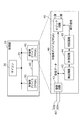
- FIG. 1 is a block diagram illustrating a configuration example of a display device according to an embodiment.
- FIG. 2 is a block diagram illustrating a configuration example of the control unit in the embodiment.
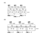
- FIG. 3 is a diagram illustrating a configuration example of a communication frame transmitted to the transmission line in the embodiment.
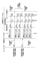
- FIG. 4 is a diagram illustrating an example of a communication sequence between the microcomputer, the first semiconductor chip, and the second semiconductor chip.
- FIG. 5 is a diagram illustrating another communication sequence example between the microcomputer, the first semiconductor chip, and the second semiconductor chip.
- FIG. 6 is a flowchart showing the state transition of the semiconductor device on the transmission side.
- FIG. 7 is a flowchart showing an operation example involving state transition of the semiconductor device on the receiving side.
- FIG. 8 is a flowchart illustrating an example of processing in the first operation state of the semiconductor device on the receiving side.
- FIG. 9 is a flowchart illustrating an example of processing in the second operation state of the semiconductor device on the receiving
- data other than the video signal may be received as the video signal immediately after the semiconductor device on the receiving side is switched to the operation mode for receiving the video signal, and the image may be disturbed.
- the microcomputer instructs each of the transmission-side semiconductor device and the reception-side semiconductor device to switch the operation mode
- erroneous data is received when the operation mode is switched.
- This can occur when there is a deviation in the instruction timing. That is, it may occur when an instruction from the microcomputer arrives first at the receiving semiconductor device and later arrives at the transmitting semiconductor device.
- the operating frequency of the microcomputer is, for example, about several hundred MHz, which is much slower.
- the transmission interface between the semiconductor devices has a high speed for transmitting some data during the deviation of the instruction from the microcomputer.
- each semiconductor device transmits a synchronization establishment signal to the microcomputer.
- the microcomputer instructs each semiconductor device to transition to an operation mode for receiving a video signal.
- the semiconductor devices perform state transition while handshaking each other. In this way, even if each semiconductor device arrives at different timings, it is possible to synchronize the state transition timing between the two semiconductor devices.
- the present disclosure provides a semiconductor device and a display device that prevent the influence of each state transition timing shift in communication between semiconductor devices without increasing costs.
- FIG. 1 is a block diagram illustrating a configuration example of the display device according to the first embodiment.
- the display device 1 shown in the figure includes a display panel substrate 20, gate drive circuits 12 a and 12 b, a source drive circuit 14, and a control unit 33.
- the display device 1 is a flat panel display device, and is an organic EL display device, a liquid crystal display device, a plasma display device, or the like. In the following description, it is assumed that the display device 1 is an organic EL display device.
- the display panel substrate 20 includes a plurality of pixel circuits 16 arranged in a matrix.
- the plurality of pixel circuits 16 are formed on the display panel substrate 20 by a semiconductor process.
- the material of the display panel substrate 20 is glass or resin (for example, acrylic).
- the plurality of pixel circuits 16 are arranged in n rows and m columns. n and m differ depending on the size and resolution of the display screen. For example, when the pixel circuit 16 corresponding to the RGB three primary colors is adjacent in a row at a resolution called HD (High Definition), n is at least 1080 rows and m is at least 1920 ⁇ 3 columns.
- HD High Definition
- Each pixel circuit 16 has an organic EL element as a light emitting element, and constitutes a light emitting pixel of any of the three primary colors RGB.
- the gate drive circuit 12 a is also called a row drive circuit, and scans the gate signal in units of rows of the pixel circuit 16.
- the gate signal is a signal input to the gate of each switch transistor in the pixel circuit 16 and is a signal for controlling on / off of the switch transistor.
- the gate drive circuit 12b has the same configuration as the gate drive circuit 12a.
- the gate drive circuits 12a and 12b drive the same gate signal at the same timing from the opposite left and right sides of the display panel substrate 20. This is to suppress signal deterioration due to the wiring capacity of each signal line in a large display device. In a small display device, only one of the gate drive circuits 12a or 12b is required.
- the source drive circuit 14 is also called a column drive circuit, and represents the brightness of pixels belonging to each column on the D (1) to D (m) signal lines based on the video signal input from the control unit 33.
- Supply voltage That is, a voltage representing the brightness of each pixel is supplied to the D (1) to D (m) signal lines.
- the supplied voltage is written into the pixel circuit 16 belonging to the selected row in the scanning of the gate drive circuits 12a and 12b.
- the video signal input from the control unit 33 to the source driving circuit 14 is input as digital serial data for each of the three primary colors of RGB, for example, converted into parallel data in units of rows in the source driving circuit 14, and It is converted to analog data in units and output to the D (1) to D (m) signal lines.
- a large display device may be provided with two source driving circuits on the upper and lower sides and output the same signal at the same timing.
- the control unit 33 controls the operation of the entire display device 1. Specifically, the control unit 33 instructs the gate driving circuits 12a and 12b to start scanning in accordance with the vertical synchronizing signal and horizontal synchronizing signal of the video signal from the outside, and the source driving circuit 14 described above. Supply digital serial data.
- FIG. 2 is a block diagram illustrating a configuration example of the control unit 33.
- the control unit 33 includes a microcomputer 30, a semiconductor device 40 that is a first semiconductor chip, and a semiconductor device 50 that is a second semiconductor chip, and has a function as a TCON (Timing Controller). .
- TCON Transmission Controller
- the semiconductor device 50 differs depending on its own operating state.
- a communication frame having a period is transmitted, and the semiconductor device 40 is configured to transition the operation state of the semiconductor device 40 in accordance with the period of the received communication frame.
- the microcomputer 30 controls the operation of the semiconductor device 40 and the semiconductor device 50. Specifically, the microcomputer 30 sends a notification that instructs the semiconductor device 40 and the semiconductor device 50 to change the operation state (or operation mode).
- the semiconductor device 40 is a semiconductor chip, and is configured, for example, as an FPGA (Field Programmable Gate Array) or an ASIC (Application Specific Integrated Circuit).
- the semiconductor device 40 supplies various control signals to the gate drive circuits 12 a and 12 b and the source drive circuit 14 in order to control display on the display panel substrate 20.
- the semiconductor device 40 has at least two operation states of the first and second operation states. That is, in the first operation state, the semiconductor device 40 processes a communication frame received from the semiconductor device 50 via the transmission line 60 as data other than the digital video signal. In the second operation state, the semiconductor device 40 processes a communication frame received from the semiconductor device 50 via the transmission line 60 as a digital video signal.
- the semiconductor device 40 transitions the operation state according to the notification from the microcomputer 30 and the period of the received communication frame.
- the semiconductor device 50 is a semiconductor chip, and is configured as, for example, an FPGA (Field Programmable Gate Array) or an ASIC (Application Specific Integrated Circuit).
- the semiconductor device 50 has at least two operation states of the first and second operation states. That is, in the first operation state, the semiconductor device 50 transmits data other than the digital video signal to the semiconductor device 40 through the transmission line 60 as a communication frame having a period T1. In the second operation state, the semiconductor device 50 transmits a digital video signal as a communication frame having a period T2 to the semiconductor device 40 via the transmission line 60.
- the semiconductor device 50 changes its operating state in response to a notification from the microcomputer 30.
- the control unit 33 is configured as described above.
- the semiconductor device 40 includes a reception circuit 42, a detection circuit 43, a measurement circuit 44, a determination circuit 45, a logic circuit 46, and a transmission line 60.
- the receiving circuit 42 receives a communication frame transmitted from the semiconductor device 50 via the transmission line 60 at a first period T1 or a second period T2 different from each other.
- the communication frame includes a synchronization code and data.
- the transmission line 60 has signal line pairs 60p and 60n that can be transmitted at high speed by LVDS (Low Voltage Voltage differential).
- the detection circuit 43 detects the synchronization code from the communication frame received by the reception circuit 42.
- the measurement circuit 44 measures the period of the synchronization code detected in a plurality of communication frames.
- the determination circuit 45 determines whether the measured cycle is the first cycle T1 or the second cycle T2.
- the logic circuit 46 has a first operation state in which the communication frame received by the reception circuit 42 is processed as data other than the digital video signal, and a second operation state in which the communication frame received by the reception circuit 42 is processed as a digital video signal. And have. Further, the logic circuit 46 transitions to the first operation state or the second operation state according to the determination result of the determination circuit 45.
- the logic circuit 46 can prevent, for example, data that is not a video signal from being processed as a video signal by using the period of the synchronization code as a condition for the transition of the operation state.
- FIG. 3 is a diagram illustrating a configuration example of a communication frame transmitted to the transmission line 60.
- FIG. 3A shows the communication frame 1 transmitted from the semiconductor device 50 in the first operation state to the semiconductor device 40 via the transmission line 60.
- the communication frame 1 has a synchronization code and data (more precisely, a payload carrying data).
- the period of the synchronization code in the plurality of communication frames 1 is the first period T1.
- the payload of the communication frame 1 carries data other than the video signal, for example, control data or dummy data for the semiconductor device 40.
- FIG. 3B shows the communication frame 2 transmitted from the semiconductor device 50 in the second operation state to the semiconductor device 40 through the transmission line 60.
- the communication frame 2 has a synchronization code and data (more precisely, a payload carrying data).
- the period of the synchronization code in the plurality of communication frames 2 is the second period T2.
- T2 the cycle T2> T1
- T2 and T1 need only be different
- a video signal is carried in the payload of the communication frame 2.
- the video signal includes, for example, data representing pixel values of any of the three primary colors of RGB, data representing a horizontal synchronization signal, data representing a vertical synchronization signal, and the like.
- FIG. 4 is a diagram illustrating a communication sequence example between the microcomputer 30, the second semiconductor chip (that is, the semiconductor device 50), and the first semiconductor chip (that is, the semiconductor device 40).
- the line extending downward from the microcomputer 30 represents the positive time axis.
- the time axis is similarly expressed for lines extending downward from the semiconductor device 50, the receiving circuit 42, the determination circuit 45, and the logic circuit 46 in FIG.
- a horizontal arrow represents a notification from the microcomputer 30 or a communication frame from the semiconductor device 50.
- T1 or T2 added to the line extending downward from the determination circuit 45 represents the determination result of the determination circuit 45.
- “OK” added to a line extending downward from the logic circuit 46 indicates that the communication frame is accepted and processed by the logic circuit 46, and “NG” is discarded without accepting the communication frame by the logic circuit 46. Represents.
- the microcomputer 30 makes a notification (T40) instructing the semiconductor device 40 to make a transition from the first operation state to the second operation state, and makes a transition to the semiconductor device 50 from the first operation state to the second operation state.
- a notification (T50) instructing this is sent is shown.
- the semiconductor device 50 and the semiconductor device 40 are each operating in the first operation state.
- a plurality of communication frames 1 (S40) from the semiconductor device 50 are received by the receiving circuit 42, the determination circuit 45 determines that the cycle is T1, is received by the logic circuit 46, and is normal data. It is processed.
- the semiconductor device 50 is in the first operation state
- the semiconductor device 40 is in the second operation state
- the operation state is shifted.
- a plurality of communication frames 1 (S41, S42) from the semiconductor device 50 are received by the reception circuit 42, determined by the determination circuit 45 to have a period T1, and received by the logic circuit 46. Without being destroyed.
- the reason for discarding is that the logic circuit 46 accepts only the communication frame of the cycle T2 in the second operation state. Therefore, it is possible to prevent the logic circuit 46 from processing data that is not a video signal as a video signal during this period. That is, in such a state deviation period, it is possible to prevent a problem due to a mismatch between the operation states of the semiconductor device 50 and the semiconductor device 40.
- both the semiconductor device 50 and the semiconductor device 40 are in the second operation state.
- a plurality of communication frames 2 (S43 to S45) from the semiconductor device 50 are received by the receiving circuit 42, the determination circuit 45 determines that the cycle is T2, is received by the logic circuit 46, and is received as a video signal. Is processed as As a result, it is displayed on the display panel substrate 20.
- FIG. 5 is a diagram illustrating another communication sequence example between the microcomputer 30, the first semiconductor chip (that is, the semiconductor device 50), and the second semiconductor chip (that is, the semiconductor device 40).
- FIG. 5 is different from FIG. 4 in that the order of the notification T50 and the notification T40 from the microcomputer is reversed.
- the semiconductor device 50 and the semiconductor device 40 are operating in the first operation state.
- a plurality of communication frames 1 (S50) from the semiconductor device 50 are received by the receiving circuit 42, the determination circuit 45 determines that the cycle is T1, and is received by the logic circuit 46, as normal data. It is processed.
- the semiconductor device 50 is in the second operation state, the semiconductor device 40 is in the first operation state, and the operation state is shifted.
- a plurality of communication frames 2 (S51, S52) from the semiconductor device 50 are received by the reception circuit 42, the determination circuit 45 determines that the cycle is T2, and is received by the logic circuit 46. Without being destroyed.
- the reason for discarding is that the logic circuit 46 accepts only the communication frame 1 of the cycle T1 in the first operation state. In this way, it is possible to prevent the logic circuit 46 from receiving and processing the video signal as data other than the video signal during this period. That is, it is possible to prevent a malfunction due to a mismatch between the operation states of the semiconductor device 50 and the semiconductor device 40.
- both the semiconductor device 50 and the semiconductor device 40 are in the second operation state.
- a plurality of communication frames 2 (S53 to S55) from the semiconductor device 50 are received by the receiving circuit 42, the determination circuit 45 determines that the cycle is T2, is received by the logic circuit 46, and is received as a video signal. Is processed as As a result, it is displayed on the display panel substrate 20.
- the semiconductor device 40 discards the communication frame if the period of the communication frame does not correspond to the operation state, so that the video signal is processed as data other than the video signal, and the data other than the video signal. Can be prevented from being processed as a video signal.
- FIG. 6 is a flowchart showing state transition of the semiconductor device 50 on the transmission side.
- the semiconductor device 50 determines whether the notification is a state transition instruction (S61), and the notification transitions to the second operation state.
- the second operation state S62
- the period of the communication frame transmitted to the transmission line 60 is changed to T2 (S63).
- the semiconductor device 50 transitions to the first operation state (S64), and changes the cycle of the communication frame transmitted to the transmission line 60 to T1 ( S65).
- the semiconductor device 50 transitions the operation state only in accordance with the notification from the microcomputer 30.
- FIG. 7 is a flowchart showing an operation example involving state transition of the semiconductor device 40 on the receiving side.
- the logic circuit 46 in the semiconductor device 40 first determines whether or not a notification of state transition has been received from the microcomputer 30 (S70). When the notification is received (Yes in S70), the logic circuit 46 further determines which state the transition instruction is (S72), and when it is determined that the transition instruction is the first operation state, the logic circuit 46 Transition to the 1st operation state (S73), when it determines with the transition instruction
- the logic circuit 46 transitions to the first operation state in which the communication frame is processed as data other than the video signal when the notification received last from the microcomputer 30 instructs the transition to the first operation state. To do. Similarly, when the notification received last indicates a transition to the second operation state, the logic circuit 46 transitions to the second operation state for processing as a communication frame and a video signal.
- the logic circuit 46 determines whether the receiving circuit 42 has received a communication frame (S71). When it is determined that the communication frame is not received (No in S71), the logic circuit 46 returns to the process of Step S70, and when it is determined that the communication frame is received (Yes in S71), the current operation state is determined. (S75). Further, when it is determined that the current operation state is the first operation state, the logic circuit 46 performs processing of the first operation state (S76), and when it is determined that the current operation state is the second operation state. Performs processing of the second operation state (S77).
- FIG. 8 is a flowchart showing a processing example in the first operation state of the semiconductor device 40 on the receiving side.
- the logic circuit 46 determines the cycle of the communication frame received in step S71 by the determination circuit 45 (S80). If the determined cycle is T2 (T2 in S80), the communication frame is discarded. (S81) If the determined cycle is T1 (T1 in S80), data processing of the communication frame is performed (S82). Specifically, the received communication frame is processed as data other than the digital video signal.
- FIG. 9 is a flowchart showing a processing example in the second operation state of the semiconductor device 40 on the receiving side.
- the logic circuit 46 determines the cycle of the communication frame received in step S71 by the determination circuit 45 (S90), and discards the communication frame if the determined cycle is T1 (T1 in S90). (S91) If the determined cycle is T2 (T2 in S90), data processing of the communication frame is performed (S92). Specifically, the received communication frame is processed as a digital video signal.
- the logic circuit 46 receives and processes the communication frame when the operation state instructed by the notification from the microcomputer 30 corresponds to the cycle of the communication frame from the semiconductor device 50.
- the logic circuit 46 receives the reception circuit 42 when the notification last received from the microcomputer 30 instructs the transition to the first operation state and the determination result by the determination circuit 45 does not indicate the first cycle.
- the communication frame received by is discarded.
- the discarding of the communication frame corresponds to step S81 in FIG. 8, and is performed during the shift period shown in FIG.
- the shift period in this state is a period in which a shift in the operating state between the semiconductor device 50 on the transmission side and the semiconductor device 40 on the reception side occurs.
- the receiving-side semiconductor device 40 is formally in the first operation state during the shift period of this state, but is substantially the first in that it does not perform a meaningful process scheduled in the first operation state. Not operating.
- the state deviation period is also a state transition period in the middle of a state transition that has not reached an operation state in which substantial processing is performed.
- the receiving-side semiconductor device 40 is substantially in the case where the formal first operation state corresponds to the cycle T1 of the received communication frame. Therefore, the first operation state is established.
- the process shown in FIG. 8 is a process in the formal first operation state
- step S82 in FIG. 8 is a process in the substantial first operation state.
- the logic circuit 46 receives the reception circuit 42.
- the communication frame received by is discarded. This discarding of the communication frame corresponds to step S91 in FIG. 9, and is performed during the shift period shown in FIG.
- the receiving-side semiconductor device 40 is formally in the second operation state, but substantially does not perform the meaningful processing scheduled in the second operation state. Not operating.
- the state deviation period is a state transition period in the middle of a state transition that has not reached an operation state in which substantial processing is performed. For example, as in the case of receiving a communication frame in FIG.
- the receiving-side semiconductor device 40 is substantially in the case where the formal second operation state corresponds to the cycle T2 of the received communication frame. Therefore, the second operation state is established.
- the process shown in FIG. 9 is a process in the formal second operation state
- step S92 in FIG. 9 is a process in the substantial second operation state.
- the logic circuit 46 discards the communication frame when the operation state instructed by the notification from the microcomputer 30 does not correspond to the cycle of the communication frame from the semiconductor device 50. Thereby, the logic circuit 46 processes the video signal as data other than the video signal and processes the data other than the video signal as the video signal due to a shift in notification timing from the microcomputer 30 and a shift in state transition. This can be prevented.
- the semiconductor device is the semiconductor device 40 that controls display on the display panel, and is transmitted in a first cycle or a second cycle that are different from each other.
- a receiving circuit 42 that receives a communication frame including: a first operating state in which the communication frame received by the receiving circuit 42 is processed as data other than a digital video signal; and a communication frame received by the receiving circuit 42
- a logic circuit 46 having a second operation state to be processed as a signal; a detection circuit 43 for detecting a synchronization code from a communication frame received by the reception circuit 42; and measuring a period of the synchronization code detected in a plurality of communication frames Measuring circuit 44 to determine whether the measured period is the first period or the second period
- a determination circuit 45 a constant to the logic circuit 46 is substantially shifts to the first operating state or the second operational state in accordance with the determination result of the determination circuit 45.
- the semiconductor device 40 receives a notification instructing the transition to the first or second operation state from the outside, and the logic circuit 46 instructs the transition to the first operation state in the last received notification,
- the determination result by the determination circuit 45 indicates the first cycle
- the state substantially transits to the first operation state
- the notification received last indicates the transition to the second operation state
- the determination circuit 45 When the determination result by indicates the second cycle, the state may be substantially shifted to the second operation state.
- the video signal is processed as data other than the video signal and the data other than the video signal is processed as the video signal due to a difference in timing of notification from the outside and a shift in state transition between the semiconductor devices. This can be prevented.
- the logic circuit 46 is received by the reception circuit 42 when the last received notification indicates a transition to the first operation state and the determination result by the determination circuit 45 does not indicate the first period. Received by the receiving circuit 42 when the last received notification indicates a transition to the second operation state and the determination result by the determination circuit 45 does not indicate the second cycle. The communication frame may be discarded.
- the semiconductor device 40 includes a row driving circuit (gate driving circuit 12a) for driving a display panel having a plurality of pixels arranged in a matrix in units of pixel rows, and column driving for driving the display panel in units of pixel columns.
- the circuit (source driver circuit 14) may be controlled.
- the semiconductor device 40 may be an FPGA (Field Programmable Gate Array).
- a display device includes a first semiconductor chip that is the semiconductor device 40, a second semiconductor chip (semiconductor device 50) that transmits a communication frame to the first semiconductor chip in one direction, A microcomputer 30 that outputs a notification instructing transition to the first or second operation state to the first and second semiconductor chips, a display panel having a plurality of pixels arranged in a matrix, and the first semiconductor chip And a column driving circuit 14 that drives the pixel column of the display panel controlled by the first semiconductor chip, and the second semiconductor chip has the first operation.
- the communication frame After receiving the notification instructing the transition to the state, the communication frame is transmitted in the first cycle, and after receiving the notification instructing the transition to the second operation state, the communication frame is transmitted in the second cycle. To send.
- the logic circuit 46 substantially enters the first operation state when the last received notification indicates a transition to the first operation state and the determination result by the determination circuit 45 indicates the first period.
- the transition may be made to the second operation state. .
- the transmission line 60 is a pair of differential signal lines 60p and 60n is shown, but a plurality of differential signal pairs may be used.
- the transmission interface between the semiconductor devices 40 and 50 may be a communication method other than differential signals.
- the semiconductor device 40 uses the notification from the microcomputer 30 and the period of the communication frame as the condition for the state transition, but only the period of the communication frame may be the condition for the state transition.
- each of the semiconductor device 40 and the semiconductor device 50 has the first operation state and the second operation state has been described.
- the semiconductor device 40 has three or more operation states. May be.
- the present disclosure can be used for a semiconductor device that controls a display panel substrate of a flat panel display device such as a television receiver or an information device, and a display device using the semiconductor device.
Landscapes
- Engineering & Computer Science (AREA)
- Physics & Mathematics (AREA)
- Computer Hardware Design (AREA)
- General Physics & Mathematics (AREA)
- Theoretical Computer Science (AREA)
- Multimedia (AREA)
- Control Of Indicators Other Than Cathode Ray Tubes (AREA)
- Communication Control (AREA)
- Synchronisation In Digital Transmission Systems (AREA)
Abstract
Description
本発明者は、「背景技術」の欄において記載した従来の高速伝送に関し、以下の問題があることを見出した。
以下、適宜図面を参照しながら、実施の形態を詳細に説明する。但し、必要以上に詳細な説明は省略する場合がある。例えば、既によく知られた事項の詳細説明や実質的に同一の構成に対する重複説明を省略する場合がある。これは、以下の説明が不必要に冗長になるのを避け、当業者の理解を容易にするためである。
図1は、実施の形態1における表示装置の構成例を示すブロック図である。同図の表示装置1は、表示パネル基板20、ゲート駆動回路12a、12b、ソース駆動回路14、制御部33を備える。表示装置1は、フラットパネル表示装置であり、有機EL表示装置、液晶表示装置、プラズマ表示装置等である。以下では、表示装置1が有機EL表示装置であるものとして説明する。
次に、制御部33の構成について説明する。
図2の下側に示すように、半導体デバイス40は、受信回路42、検出回路43、計測回路44、判定回路45、ロジック回路46、伝送線60を備える。
続いて、通信フレームの構成について説明する。
図4は、マイコン30、第2の半導体チップ(つまり半導体デバイス50)および第1の半導体チップ(つまり半導体デバイス40)の間の通信シーケンス例を示す図である。
続いて、送信側の半導体デバイス50の状態遷移について説明する。
次に、受信側の半導体デバイス40の状態遷移を伴う動作例について説明する。
以上、半導体デバイス、それを用いた表示装置について、実施の形態に基づいて説明したが、本開示は、この実施の形態に限定されるものではない。本開示の趣旨を逸脱しない限り、当業者が思いつく各種変形を本実施の形態に施したものや、異なる実施の形態における構成要素を組み合わせて構築される形態も、一つまたは複数の態様の範囲内に含まれても良い。
12a、12b ゲート駆動回路
14 ソース駆動回路
16 画素回路
20 表示パネル基板
30 マイコン
33 制御部
35 バス
40、50 半導体デバイス
42 受信回路
43 検出回路
44 計測回路
45 判定回路
46 ロジック回路
60 伝送線
Claims (7)
- 表示パネルの表示を制御する半導体デバイスであって、
互いに異なる第1の周期または第2の周期で送信され、同期コードとデータとを含む通信フレームを受信する受信回路と、
前記受信回路によって受信された前記通信フレームをデジタル映像信号以外のデータとして処理する第1動作状態と、前記受信回路によって受信された前記通信フレームをデジタル映像信号として処理する第2動作状態とを有するロジック回路と、
前記受信回路によって受信された前記通信フレームから同期コードを検出する検出回路と、
複数の前記通信フレームにおいて検出された前記同期コードの周期を計測する計測回路と、
計測された周期が前記第1の周期であるか前記第2の周期であるかを判定する判定回路とを備え、
前記ロジック回路は、前記判定回路の判定結果に応じて前記第1動作状態または前記第2動作状態に実質的に移行する
半導体デバイス。 - 前記半導体デバイスは、前記第1または前記第2動作状態への遷移を指示する通知を外部から受信し、
前記ロジック回路は、
最後に受信した前記通知が前記第1動作状態への遷移を指示し、かつ、前記判定回路による判定結果が前記第1の周期を示すとき、前記第1動作状態に実質的に遷移し、
最後に受信した前記通知が前記第2動作状態への遷移を指示し、かつ、前記判定回路による判定結果が前記第2の周期を示すとき、前記第2動作状態に実質的に遷移する
請求項1に記載の半導体デバイス。 - 前記ロジック回路は、
最後に受信した前記通知が前記第1動作状態への遷移を指示し、かつ、前記判定回路による判定結果が前記第1の周期を示していないとき、前記受信回路によって受信された通信フレームを破棄し、
最後に受信した前記通知が前記第2動作状態への遷移を指示し、かつ、前記判定回路による判定結果が前記第2の周期を示していないとき、前記受信回路によって受信された通信フレームを破棄する
請求項1または2に記載の半導体デバイス。 - 前記半導体デバイスは、
行列状に配置された複数の画素を有する前記表示パネルを画素行単位に駆動する行駆動回路と、前記表示パネルを画素列単位に駆動する列駆動回路とを制御する
請求項1~3の何れか1項に記載の半導体デバイス。 - 前記半導体デバイスはFPGA(Field Programmable Gate Array)である
請求項1~4の何れか1項に記載の半導体デバイス。 - 請求項1に記載の半導体デバイスである第1の半導体チップと、
前記通信フレームを前記第1の半導体チップに一方向に送信する第2の半導体チップと、
前記第1または前記第2動作状態への遷移を指示する通知を前記第1および前記第2の半導体チップに出力するマイコンと、
行列状に配置された複数の画素を有する表示パネルと、
前記第1の半導体チップにより制御され前記表示パネルの画素行を駆動する行駆動回路と、
前記第1の半導体チップにより制御され前記表示パネルの画素列を駆動する列駆動回路と
を備え、
前記第2半導体チップは、前記第1動作状態への遷移を指示する前記通知を受けた後、前記通信フレームを前記第1の周期で送信し、前記第2動作状態への遷移を指示する前記通知を受けた後、前記通信フレームを前記第2の周期で送信する
表示装置。 - 前記ロジック回路は、
最後に受信した前記通知が前記第1動作状態への遷移を指示し、かつ、前記判定回路による判定結果が前記第1の周期を示すとき、前記第1動作状態に実質的に遷移し、
最後に受信した前記通知が前記第2動作状態への遷移を指示し、かつ、前記判定回路による判定結果が前記第2の周期を示すとき、前記第2動作状態に実質的に遷移する
請求項6に記載の表示装置。
Priority Applications (2)
| Application Number | Priority Date | Filing Date | Title |
|---|---|---|---|
| US15/123,087 US10460654B2 (en) | 2014-03-06 | 2014-12-17 | Semiconductor device and display apparatus |
| JP2016505946A JP6312101B2 (ja) | 2014-03-06 | 2014-12-17 | 半導体デバイスおよび表示装置 |
Applications Claiming Priority (2)
| Application Number | Priority Date | Filing Date | Title |
|---|---|---|---|
| JP2014-044322 | 2014-03-06 | ||
| JP2014044322 | 2014-03-06 |
Publications (1)
| Publication Number | Publication Date |
|---|---|
| WO2015132833A1 true WO2015132833A1 (ja) | 2015-09-11 |
Family
ID=54054678
Family Applications (1)
| Application Number | Title | Priority Date | Filing Date |
|---|---|---|---|
| PCT/JP2014/006303 Ceased WO2015132833A1 (ja) | 2014-03-06 | 2014-12-17 | 半導体デバイスおよび表示装置 |
Country Status (3)
| Country | Link |
|---|---|
| US (1) | US10460654B2 (ja) |
| JP (1) | JP6312101B2 (ja) |
| WO (1) | WO2015132833A1 (ja) |
Families Citing this family (1)
| Publication number | Priority date | Publication date | Assignee | Title |
|---|---|---|---|---|
| CN109509422B (zh) * | 2018-12-27 | 2021-08-24 | 惠科股份有限公司 | 显示面板驱动电路及显示装置 |
Citations (4)
| Publication number | Priority date | Publication date | Assignee | Title |
|---|---|---|---|---|
| JP2006235151A (ja) * | 2005-02-24 | 2006-09-07 | Fujitsu Hitachi Plasma Display Ltd | 表示パネルの表示制御装置及びそれを有する表示装置 |
| JP2008076989A (ja) * | 2006-09-25 | 2008-04-03 | Matsushita Electric Ind Co Ltd | 表示装置、携帯電話装置、情報端末装置、および表示方法 |
| JP2009042659A (ja) * | 2007-08-10 | 2009-02-26 | Toshiba Matsushita Display Technology Co Ltd | 液晶表示装置 |
| JP2011221487A (ja) * | 2010-04-05 | 2011-11-04 | Silicon Works Co Ltd | クロック信号がエンベッディングされた単一レベルのデータ伝送を利用したディスプレイ駆動システム |
Family Cites Families (14)
| Publication number | Priority date | Publication date | Assignee | Title |
|---|---|---|---|---|
| DE3722169C2 (de) * | 1987-07-04 | 1997-06-05 | Thomson Brandt Gmbh | Verfahren und Vorrichtung zur Durchführung des Verfahrens zur Anpassung eines Mehrbetriebsarten-Monitors an einen Personal Computer |
| US5926174A (en) * | 1995-05-29 | 1999-07-20 | Canon Kabushiki Kaisha | Display apparatus capable of image display for video signals of plural kinds |
| JPH09218670A (ja) * | 1996-02-14 | 1997-08-19 | Fujitsu Ltd | 表示モード判別機能付き表示装置および表示モード判別方法 |
| JP3971892B2 (ja) | 2000-09-08 | 2007-09-05 | 株式会社日立製作所 | 液晶表示装置 |
| US7221381B2 (en) | 2001-05-09 | 2007-05-22 | Clairvoyante, Inc | Methods and systems for sub-pixel rendering with gamma adjustment |
| KR100720652B1 (ko) * | 2005-09-08 | 2007-05-21 | 삼성전자주식회사 | 디스플레이 구동 회로 |
| TWI397055B (zh) * | 2007-05-28 | 2013-05-21 | Realtek Semiconductor Corp | 模式偵測電路與方法 |
| US9112520B2 (en) * | 2010-08-12 | 2015-08-18 | Mediatek Inc. | Transmission interface and system using the same |
| US8648739B2 (en) * | 2010-08-12 | 2014-02-11 | Mediatek Inc. | Transmission interface and system using the same |
| US8941592B2 (en) * | 2010-09-24 | 2015-01-27 | Intel Corporation | Techniques to control display activity |
| DE102012107954B4 (de) * | 2011-09-02 | 2025-12-18 | Samsung Electronics Co. Ltd. | Anzeigetreiber, Betriebsverfahren davon, Host zur Steuerung des Anzeigetreibers und System mit dem Anzeigetreiber und dem Host |
| US9818375B2 (en) * | 2012-09-28 | 2017-11-14 | Sharp Kabushiki Kaisha | Liquid-crystal display device and drive method thereof |
| KR102009885B1 (ko) * | 2012-10-30 | 2019-08-12 | 엘지디스플레이 주식회사 | 표시장치 및 이의 구동방법 |
| WO2014103918A1 (ja) * | 2012-12-28 | 2014-07-03 | シャープ株式会社 | 液晶表示装置およびその駆動方法 |
-
2014
- 2014-12-17 JP JP2016505946A patent/JP6312101B2/ja active Active
- 2014-12-17 WO PCT/JP2014/006303 patent/WO2015132833A1/ja not_active Ceased
- 2014-12-17 US US15/123,087 patent/US10460654B2/en active Active
Patent Citations (4)
| Publication number | Priority date | Publication date | Assignee | Title |
|---|---|---|---|---|
| JP2006235151A (ja) * | 2005-02-24 | 2006-09-07 | Fujitsu Hitachi Plasma Display Ltd | 表示パネルの表示制御装置及びそれを有する表示装置 |
| JP2008076989A (ja) * | 2006-09-25 | 2008-04-03 | Matsushita Electric Ind Co Ltd | 表示装置、携帯電話装置、情報端末装置、および表示方法 |
| JP2009042659A (ja) * | 2007-08-10 | 2009-02-26 | Toshiba Matsushita Display Technology Co Ltd | 液晶表示装置 |
| JP2011221487A (ja) * | 2010-04-05 | 2011-11-04 | Silicon Works Co Ltd | クロック信号がエンベッディングされた単一レベルのデータ伝送を利用したディスプレイ駆動システム |
Also Published As
| Publication number | Publication date |
|---|---|
| US10460654B2 (en) | 2019-10-29 |
| JP6312101B2 (ja) | 2018-04-18 |
| US20170076662A1 (en) | 2017-03-16 |
| JPWO2015132833A1 (ja) | 2017-03-30 |
Similar Documents
| Publication | Publication Date | Title |
|---|---|---|
| JP5766403B2 (ja) | 液晶ディスプレーの駆動回路および駆動方法 | |
| US11120724B2 (en) | Display device and driving method thereof | |
| KR102043532B1 (ko) | 액정 패널의 구동 회로 및 액정 디스플레이 장치 | |
| CN105282471B (zh) | 多画面显示装置 | |
| KR102219091B1 (ko) | 표시장치 | |
| US10388209B2 (en) | Interface circuit | |
| US10008140B2 (en) | Bright dot detection method and display panel | |
| US9805682B2 (en) | Scanning driving circuits and the liquid crystal devices with the same | |
| CN104793827A (zh) | 一种阵列基板和自电容式触控显示装置 | |
| US9165532B2 (en) | Display device | |
| US12494156B2 (en) | Data receiving device, data receiving method, and data communication system | |
| CN114267293A (zh) | 显示装置及其显示方法 | |
| US9349339B2 (en) | Pre-charging apparatus of source driving circuit and operating method thereof | |
| JP6312101B2 (ja) | 半導体デバイスおよび表示装置 | |
| JP6465583B2 (ja) | タイミングコントローラおよびそれを用いたディスプレイ装置 | |
| JP6286142B2 (ja) | 表示装置、及びソースドライバ | |
| KR102439570B1 (ko) | 표시장치 및 그 구동방법 | |
| US9437151B2 (en) | Scan driving circuit and display panel | |
| JP6999053B2 (ja) | インタフェース回路 | |
| KR100726987B1 (ko) | 소형-저전압 차동 신호 수신칩 | |
| US9343037B2 (en) | Data transmission method and display device | |
| WO2013051223A1 (ja) | 画像データ信号出力装置、画像データ信号入力装置、および画像表示装置 | |
| JP2025058637A (ja) | 表示装置及びソースドライバ | |
| JP2015082719A (ja) | 映像信号処理装置 | |
| KR20100120411A (ko) | 유기전계발광표시장치 및 그의 구동방법 |
Legal Events
| Date | Code | Title | Description |
|---|---|---|---|
| 121 | Ep: the epo has been informed by wipo that ep was designated in this application |
Ref document number: 14884462 Country of ref document: EP Kind code of ref document: A1 |
|
| ENP | Entry into the national phase |
Ref document number: 2016505946 Country of ref document: JP Kind code of ref document: A |
|
| WWE | Wipo information: entry into national phase |
Ref document number: 15123087 Country of ref document: US |
|
| NENP | Non-entry into the national phase |
Ref country code: DE |
|
| 122 | Ep: pct application non-entry in european phase |
Ref document number: 14884462 Country of ref document: EP Kind code of ref document: A1 |