WO2015129763A1 - 表示装置 - Google Patents
表示装置 Download PDFInfo
- Publication number
- WO2015129763A1 WO2015129763A1 PCT/JP2015/055456 JP2015055456W WO2015129763A1 WO 2015129763 A1 WO2015129763 A1 WO 2015129763A1 JP 2015055456 W JP2015055456 W JP 2015055456W WO 2015129763 A1 WO2015129763 A1 WO 2015129763A1
- Authority
- WO
- WIPO (PCT)
- Prior art keywords
- light
- display device
- control film
- shutter
- base material
- Prior art date
- Legal status (The legal status is an assumption and is not a legal conclusion. Google has not performed a legal analysis and makes no representation as to the accuracy of the status listed.)
- Ceased
Links
Images





Classifications
-
- G—PHYSICS
- G02—OPTICS
- G02B—OPTICAL ELEMENTS, SYSTEMS OR APPARATUS
- G02B26/00—Optical devices or arrangements for the control of light using movable or deformable optical elements
- G02B26/02—Optical devices or arrangements for the control of light using movable or deformable optical elements for controlling the intensity of light
- G02B26/04—Optical devices or arrangements for the control of light using movable or deformable optical elements for controlling the intensity of light by periodically varying the intensity of light, e.g. using choppers
-
- G—PHYSICS
- G02—OPTICS
- G02B—OPTICAL ELEMENTS, SYSTEMS OR APPARATUS
- G02B26/00—Optical devices or arrangements for the control of light using movable or deformable optical elements
- G02B26/02—Optical devices or arrangements for the control of light using movable or deformable optical elements for controlling the intensity of light
- G02B26/023—Optical devices or arrangements for the control of light using movable or deformable optical elements for controlling the intensity of light comprising movable attenuating elements, e.g. neutral density filters
-
- G—PHYSICS
- G02—OPTICS
- G02B—OPTICAL ELEMENTS, SYSTEMS OR APPARATUS
- G02B5/00—Optical elements other than lenses
- G02B5/003—Light absorbing elements
-
- G—PHYSICS
- G02—OPTICS
- G02B—OPTICAL ELEMENTS, SYSTEMS OR APPARATUS
- G02B5/00—Optical elements other than lenses
- G02B5/02—Diffusing elements; Afocal elements
- G02B5/0205—Diffusing elements; Afocal elements characterised by the diffusing properties
- G02B5/0236—Diffusing elements; Afocal elements characterised by the diffusing properties the diffusion taking place within the volume of the element
- G02B5/0247—Diffusing elements; Afocal elements characterised by the diffusing properties the diffusion taking place within the volume of the element by means of voids or pores
-
- G—PHYSICS
- G02—OPTICS
- G02B—OPTICAL ELEMENTS, SYSTEMS OR APPARATUS
- G02B5/00—Optical elements other than lenses
- G02B5/02—Diffusing elements; Afocal elements
- G02B5/0205—Diffusing elements; Afocal elements characterised by the diffusing properties
- G02B5/0257—Diffusing elements; Afocal elements characterised by the diffusing properties creating an anisotropic diffusion characteristic, i.e. distributing output differently in two perpendicular axes
-
- G—PHYSICS
- G02—OPTICS
- G02B—OPTICAL ELEMENTS, SYSTEMS OR APPARATUS
- G02B5/00—Optical elements other than lenses
- G02B5/02—Diffusing elements; Afocal elements
- G02B5/0273—Diffusing elements; Afocal elements characterized by the use
- G02B5/0278—Diffusing elements; Afocal elements characterized by the use used in transmission
Definitions
- the present invention relates to a display device.
- This application claims priority based on Japanese Patent Application No. 2014-035173 filed in Japan on February 26, 2014, the contents of which are incorporated herein by reference.
- a MEMS display has a shutter (movable part) formed on a substrate using a semiconductor process technology, and the shutter light is opened and closed at a high speed so that light from a backlight is transmitted from a portion where the shutter is opened. Is displayed. In the MEMS display, direct light from the backlight is adjusted by opening and closing the shutter.
- One aspect of the present invention has been made in view of the above-described problems of the prior art, and is capable of displaying with high visibility by suppressing reflection due to external light and has a variation in luminance.
- One object of the present invention is to provide a display device capable of suppressing display unevenness by suppressing.
- a display device includes a display body and a light control film that controls light distribution characteristics of light emitted from the display body, and the display body includes an illumination device and the illumination device.
- a light transmissive member having an opening that transmits light emitted from the light source, and a shutter that is movably provided with respect to the opening and that switches whether light is transmitted or blocked through the opening.
- the light control film includes a light-transmitting base material, a light diffusion portion formed on the first surface of the base material, and a region other than the light diffusion portion formation region of the first surface of the base material.
- a light-shielding layer formed in a region, and the light diffusing portion has a light-emitting end surface that is in contact with the base material, and a light-incident surface that is opposed to the light-emitting end surface and has an area larger than the area of the light-emitting end surface.
- An end face, and the light exit end face to the light exit end. Height to is greater than the thickness of the light shielding layer.
- the shutter may be made of a material having light reflectivity.
- the display device may be configured such that the light control film diffuses light incident from the light incident end face anisotropically in an azimuth direction viewed from the normal direction of the base material. Good.
- the light-shielding layer includes a plurality of light-shielding layers, and the planar shape of the light-shielding layer viewed from the normal direction of the base material has a major axis and a minor axis. It is good also as a structure which is a rectangular shape.
- the opening includes a plurality of openings arranged in a matrix in a first direction and a second direction, and the first direction and the second direction
- the direction on the side where the pitch of the openings adjacent to each other is narrow and the azimuth angle direction in which the light control film has a relatively strong light diffusibility may be substantially matched.
- a display device capable of performing bright display by suppressing reflection due to external light and suppressing display unevenness by suppressing luminance variation. can do.
- FIG. 6 is a diagram illustrating a shutter operation of the shutter assembly, and a diagram illustrating a closed state of the shutter assembly.
- FIG. 7 is a diagram illustrating a shutter operation of the shutter assembly, and a diagram illustrating an open state of the shutter assembly.
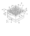
- the perspective view which shows the structure of a light control film.
- Sectional drawing which shows a light control film (ZX sectional drawing).
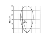
- FIG. 4 is a diagram showing the light distribution characteristics of a conventional MEMS display device (without a light control film), which is a result of measuring the light distribution characteristics (light distribution angle-luminance) of the MEMS display device in order to demonstrate the effect of the light control film.
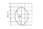
- the light distribution characteristic (light distribution angle-luminance) of the MEMS display device was measured in order to verify the effect of the light control film, and the light distribution characteristic of the MEMS display device (with the light control film) of the first embodiment.
- FIG. The perspective view which shows the MEMS display apparatus of 2nd Embodiment. The 1st figure for demonstrating the reflection of the light in the shape of the light shielding layer of a light control film, and the side surface of a light-diffusion part.
- the 2nd figure for demonstrating the reflection of the light in the shape of the light shielding layer of a light control film, and the side surface of a light-diffusion part The 3rd figure for demonstrating the reflection of the light in the shape of the light shielding layer of a light control film, and the side surface of a light-diffusion part.
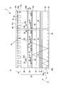
- FIG. 1 is a diagram illustrating a schematic configuration of the MEMS display device according to the first embodiment.
- FIG. 1 shows mainly a shutter-based light modulator array incorporated in a MEMS display device.
- the MEMS display device (display device) 1 includes a display body 14 and a light control film 9 that controls light distribution characteristics of light emitted from the display body 14.
- the display body 14 includes a MEMS element 13 including a plurality of shutter assemblies 19 and a backlight (illumination device) 11.
- the MEMS element 13 includes a brightness enhancement film 16, a diffuser 17, a light modulator substrate 18, a shutter assembly (light modulator) 19, and a cover plate 20.
- a plurality of shutter assemblies 19 are arranged on the light modulator substrate 18. Although only four shutter assemblies are shown in FIG. 1, in practice, a large number of shutter assemblies are arranged in the row and column directions.
- the shutter assembly 19 operates so that the state can be selectively switched between a closed state in which the passage of light from the backlight 11 is blocked and an open state in which the passage of light from the backlight 11 is allowed.
- each shutter assembly 19 is provided so as to correspond to one pixel in the display image, but a plurality of shutter assemblies 19 may be provided so as to correspond to one pixel.
- the display body 14 selectively opens one or a plurality of shutter assemblies 19 corresponding to a specific display image in the same manner as the driving of the backlight 11, and uses light that has passed through the shutter assemblies 19.
- a display image can be formed.
- FIG. 2 is a cross-sectional view showing a schematic configuration of the MEMS display device. As shown in FIG. 2, when the side on which the light control film 9 is disposed is the front side of the MEMS element 13, the backlight 11 is located behind the MEMS element 13 on the side opposite to the light control film 9.
- the backlight 11 includes one or a plurality of light sources 61, a light guide plate 62, a plurality of prisms 63, and a reflective film 64.
- the backlight 11 of the present embodiment is an edge light type backlight 11 in which a light source 61 is installed on a side end surface (light incident surface 62 a) of a light guide plate 62.
- the light source 61 is constituted by, for example, a plurality of LEDs (Light Emitting Diodes) arranged in a line, and the light emitting part of the LED is disposed so as to face the light incident surface 62 a of the light guide plate 62.
- LEDs are generally used as a backlight light source because they generally have high color purity and are superior in stability and high-speed response.
- white LED which light-emits white with one LED, and LED which light-emits each single color light of RGB are used. Wide color gamut performance can be obtained by using RGB single-color LEDs.
- white LEDs are advantageous in that they are low in cost and can reduce the total power consumption due to the number of LEDs required.
- an incandescent lamp, a fluorescent lamp, or a laser may be used.
- each light source 61 Light emitted from each light source 61 enters the light guide plate 62 from the light incident surface 62a of the light guide plate 62, is guided while being diffused inside the light guide plate 62, and is on the upper side (shutter assembly 19 side). The light exits from the light exit surface 62b.
- the light guide plate 62 is made of a transparent material, that is, glass or plastic material. Examples of the plastic material include acrylic resin, polycarbonate resin, and cycloolefin resin (COP).
- the reflection film 64 is disposed on the back side of the light guide plate 62 and reflects the light guided in the light guide plate 62 toward the shutter assembly 19 side.
- the plurality of prisms 63 are disposed on the surface of the reflective film 64 and function to efficiently guide the light incident on the light guide plate 62 toward the shutter assembly 19.
- the plurality of prisms 63 are arranged at a predetermined interval from each other, and are arranged so as to become denser as they move away from the light source 61. Note that the cross-sectional shape of the prism 63 may be a trapezoid in addition to a triangle.
- a plurality of prisms 63 may be formed integrally with the reflective film 64.
- the brightness enhancement film 16 and the diffuser 17 of the display body 14 are provided in this order.
- the light modulator substrate 18 is disposed on the light emission surface 62 b of the backlight 11 through the brightness enhancement film 16 and the diffuser 17.
- the optical modulator substrate 18 holds the shutter assembly 19 and is made of a light transmissive substrate.
- the shutter assembly 19 includes at least an aperture layer (light transmitting member) 22 and a shutter 23, and is provided on the surface of the light modulator substrate 18 (the surface opposite to the backlight 11).
- the aperture layer 22 has a plurality of openings 24 that transmit light emitted from the backlight 11.
- Each opening 24 is patterned for each shutter assembly 19.
- the plurality of openings 24 are arranged in a matrix in the longitudinal direction (first direction) and the short direction (second direction) on the surface of the optical modulator substrate 18.
- the short side direction of the optical modulator substrate 18 and the direction P on the side where the pitch of the openings 24 adjacent to each other is narrow coincide with each other.
- the aperture layer 22 is made of a reflective material or a light absorbing material.
- the aperture layer 22 of the present embodiment is made of a reflective material, and directs light that has entered a region other than the opening 24 out of the light from the backlight 11 (light that has not passed through the opening 24) toward the backlight 11. To reflect.
- the shutter 23 plays a role of switching between transmitting light from the backlight 11 through the opening 24 of the aperture layer 22 or blocking the light. It is provided so as to be movable with respect to the opening 24 of the aperture layer 22, and is configured to be movable in the horizontal direction along the surface of the aperture layer 22.
- the shutter 23 covers a substantially entire opening 24 of the aperture layer 22 so as to block light (closed state), and a passing position (open state) through which the entire opening 24 is exposed to allow light to pass. , Are selectively moved.
- the shutter 23 When the shutter assembly 19 is in the open state, the shutter 23 allows light from the backlight 11 to pass through the opening 24 of the aperture layer 22 toward the viewer (viewing side). When the shutter assembly 19 is in the closed state, the shutter 23 blocks light transmitted from the backlight 11 through the opening 24 of the aperture layer 22.
- the opening / closing operation of the shutter 23 is controlled by a control unit (not shown).
- the light modulator substrate 18 is attached to the cover plate 20 via an adhesive seal 25.
- the cover plate 20 is disposed above the shutter assembly 19.
- the back side of the cover plate 20 can be covered with a black matrix BM to enhance contrast.
- the cover plate 20 is supported at a predetermined distance from the shutter assembly 19. A gap G formed between the cover plate 20 and the shutter assembly 19 is maintained by the spacer 26 and the adhesive seal 25.
- the adhesive seal 25 seals the working fluid 21 filled in the gap G.
- the working fluid 21 functions as a lubricant.
- the working fluid 21 includes, but is not limited to, ion-removed water, methanol, ethanol, silicone oil, fluorinated silicone oil, dimethylsiloxane, polydimethylsiloxane, hexamethyldisiloxane, and diethylbenzene.
- a hydrophobic liquid may be used. The hydrophobic liquid can remove water from the surface of the shutter assembly 19. Further, the working fluid 21 may be filled with air.
- the adhesive seal 25 can be formed of a polymer adhesive such as epoxy, acrylate, or silicon material.
- the light control film 9 includes a transparent base material (base material) 39, and a light diffusion layer 44 and a light shielding layer 40 formed on the first surface 39 a of the transparent base material 39.
- the light diffusion layer 44 includes a light diffusion portion 41 and a hollow portion 43.
- the light diffusing portion 41 includes a light emitting end face 41a that is in contact with the transparent base material 39, and a light incident end face 41b that faces the light emitting end face 41a and has an area larger than the area of the light emitting end face 41a.
- the light diffusion layer 44 is configured such that the height from the light incident end face 41 b to the light exit end face 41 a is larger than the thickness of the light shielding layer 40.
- the light shielding layer 40 is formed in a region other than the region where the light diffusion portion 41 is formed on the first surface 39 a of the transparent base material 39.
- the shutter assembly 19 incorporated in the MEMS display device 1 includes two actuators 27 (first actuator 27A and second actuator 27B) coupled to the shutter 23 described above.
- the first actuator 27A and the second actuator 27B are disposed on both sides of the shutter 23 in the short direction, and are controlled independently of each other.
- the first actuator 27A functions to open the shutter 23.
- the second actuator 27B functions to close the shutter 23.
- the first actuator 27A and the second actuator 27B open and close the shutter 23 by moving the shutter 23 in a plane substantially parallel to the aperture layer 22.
- the shutter 23 is suspended at a distance from the aperture layer 22 by an anchor 28 attached to the first actuator 27A and the second actuator 27B.
- the shutter 23 has a plurality of shutter openings 23A and a light shielding region 23B.
- three shutter openings 23 ⁇ / b> A are provided corresponding to the openings 24 of the aperture layer 22.
- Each shutter opening 23 ⁇ / b> A transmits light that has passed through each opening 24 of the aperture layer 22, and the light shielding area 23 ⁇ / b> B blocks light that has passed through each opening 24 in the aperture layer 22.
- each shutter opening 23A overlaps with each of the openings 24 of the aperture layer 22 in plan view
- the light-shielding region 23B is in each aperture layer 22 It overlaps with the opening 24 in plan view.
- the shutter opening 23A is formed in a rectangular pattern similarly to the opening 24 of the aperture layer 22, and has a size including the opening 24 when it overlaps the opening 24 of the aperture layer 22 in plan view, that is, the aperture layer 22.
- the opening area is larger than that of the opening 24.
- the light shielding region 23B also has an area that can cover the entire opening 24 of the aperture layer 22. Note that the shape of the shutter opening 23A and the opening 24 of the aperture layer 22 in plan view is not limited to the above-described shape.
- the side of the shutter 23 facing the aperture layer 22 is covered with a light-absorbing substance or a light-reflective material in order to absorb or reflect the light that has been shielded.
- the shutter 23 may be made of a light absorbing material or a reflective material.
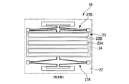
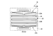
- FIGS. 3A and 3B are diagrams showing the shutter operation of the shutter assembly 19, in which FIG. 3A shows a closed state of the shutter assembly 19, and FIG. 3B shows a opened state of the shutter assembly 19.
- FIG. 4 is a perspective view showing the configuration of the light control film.
- 5A is a cross-sectional view (ZX cross-sectional view) showing the light control film
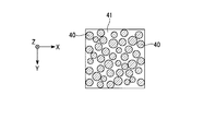
- FIG. 5B is a plan view (XY plan view) of the light control film.
- illustration of the transparent base material 39 is abbreviate
- the light control film 9 includes a transparent base material 39, and a plurality of light shielding layers 40 formed on the first surface 39a of the transparent base material 39 (the surface opposite to the viewing side), And a light diffusion layer 44 formed on the first surface 39a of the transparent substrate 39.
- This light control film 9 is not shown with respect to the cover plate 20 (FIG. 2) with the light diffusion layer 44 side facing the cover plate 20 (FIG. 2) and the transparent base material 39 side facing the viewing side. It is fixed via an adhesive layer.
- the transparent substrate 39 is made of a transparent resin such as a triacetyl cellulose (TAC) film, polyethylene terephthalate (PET), polycarbonate (PC), polyethylene naphthalate (PEN), or polyethersulfone (PES) film. Is preferably used.
- TAC triacetyl cellulose
- PET polyethylene terephthalate
- PC polycarbonate
- PEN polyethylene naphthalate
- PES polyethersulfone
- the transparent substrate 39 serves as a base when a material for the light-shielding layer 40 and the light diffusion layer 44 is applied later in a manufacturing process described later, and has heat resistance and mechanical strength in a heat treatment step during the manufacturing process. It is necessary to have. Therefore, as the transparent base material 39, a glass base material or the like may be used in addition to the resin base material.
- the total light transmittance of the transparent substrate 39 is preferably 90% or more as defined in JIS K7361-1. When the total light transmittance is 90% or more, sufficient transparency can be obtained.
- a transparent resin substrate having a thickness of 100 ⁇ m is used as an example.
- the plurality of light shielding layers 40 are formed so as to be scattered on the first surface 39 a of the transparent base material 39. As shown in FIG. 5B, the plurality of light shielding layers 40 are randomly arranged as viewed from the normal direction (Z-axis direction) of the transparent base material 39. In the present embodiment, the planar shape of each light shielding layer 40 is circular.
- the light shielding layer 40 includes a layer made of a black pigment, dye, resin, or the like having light absorption and photosensitivity, such as a black resist containing carbon black.
- a resin containing carbon black or the like since the film constituting the light shielding layer 40 can be formed in the printing process, advantages such as a small amount of material used and a high throughput can be obtained.
- a metal film such as Cr (chromium) or a Cr / Cr oxide multilayer film may be used. When this type of metal film or multilayer film is used, the optical density of these films is high, so that there is an advantage that light is sufficiently absorbed by the thin film.
- the diameter of each light shielding layer 40 is 20 micrometers as an example, and the coverage with the whole film is about 20%.
- the light diffusion layer 44 is formed on the first surface 39a of the transparent base material 39 in a region excluding the plurality of light shielding layers 40.
- the light diffusion layer 44 is made of an organic material having light transmissivity and photosensitivity such as acrylic resin and epoxy resin.
- the total light transmittance of the light diffusion layer 44 is preferably 90% or more in accordance with JIS K7361-1. When the total light transmittance is 90% or more, sufficient transparency can be obtained.
- the layer thickness of the light diffusion layer 44 is set sufficiently larger than the thickness of the light shielding layer 40. In the case of this embodiment, the layer thickness of the light diffusion layer 44 is about 25 ⁇ m as an example, and the layer thickness of the light shielding layer 40 is about 150 nm as an example.
- the light diffusion layer 44 has a light emission end face 41a, a light incident end face 41b, and a side face 41c.
- the light emission end surface 41 a is a surface in contact with the transparent substrate 39.
- the light incident end surface 41b is a surface facing the light emitting end surface 41a.
- the side surface 41 c is a tapered side surface of the light diffusion portion 41.
- the side surface 41c is a surface that reflects light incident from the light incident end surface 41b.
- the area of the light incident end face 41b is larger than the area of the light exit end face 41a.
- the light shielding layer 40 is formed so that the cross-sectional area when cut along a plane parallel to one surface of the transparent base material 39 is large on the light shielding layer 40 side and gradually decreases as the distance from the light shielding layer 40 increases.
- a hollow portion 43 is formed. That is, the hollow portion 43 has a so-called forward tapered tapered truncated cone shape when viewed from the transparent substrate 39 side. Air exists in the hollow portion 43.
- the portion other than the hollow portion 43 of the light diffusion layer 44 that is, the portion where the transparent resin is continuously present is a portion contributing to light transmission. Therefore, in the following description, a portion other than the hollow portion 43 of the light diffusion layer 44 is also referred to as a light diffusion portion 41. Light incident on the light diffusing portion 41 is totally reflected at the interface between the light diffusing portion 41 and the hollow portion 43 and guided in a state of being substantially confined inside the light diffusing portion 41, via the transparent base material 39. Is emitted to the outside.
- the light control film 9 is disposed so that the transparent base material 39 faces the viewing side. Therefore, the surface with the smaller area (transparent) of the two opposing surfaces of the light diffusion portion 41.
- the surface on the side in contact with the base material 39) becomes the light emission end surface 41a
- the surface with the larger area (surface on the side opposite to the transparent base material 39) becomes the light incident end surface 41b.
- the inclination angle (angle formed by the light emission end face 41a and the side face 41c) of the side face 41c of the light diffusing part 41 (interface between the light diffusing part 41 and the hollow part 43) is preferably about 60 ° to 85 °.
- the inclination angle of the side surface 41c of the light diffusing portion 41 is not particularly limited as long as the loss of incident light is not so large and the incident light can be sufficiently diffused.
- the light diffusion portion 41 since air exists in the hollow portion 43, if the light diffusion portion 41 is formed of, for example, a transparent acrylic resin, the side surface 41c of the light diffusion portion 41 is an interface between the transparent acrylic resin and air. It becomes.
- the difference in refractive index at the interface between the inside and the outside of the light diffusing portion 41 is such that the periphery of the light diffusing portion 41 is made of another general low refractive index material when the hollow portion 43 is filled with air. It is larger than when it is filled. Therefore, according to Snell's law, the incident angle range in which light is totally reflected by the side surface 41c of the light diffusion portion 41 is wide. As a result, light loss is further suppressed, and high luminance can be obtained.
- the hollow portion 43 may be filled with an inert gas such as nitrogen instead of air. Alternatively, the inside of the hollow portion 43 may be in a vacuum state.
- the refractive index of the transparent substrate 39 and the refractive index of the light diffusion layer 44 are substantially equal.
- the reason is that, for example, if the refractive index of the transparent base material 39 and the refractive index of the light diffusion layer 44 are greatly different, the light that has entered from the light incident end surface 41 b is diffused when attempting to exit the light diffusion layer 44. This is because unnecessary refraction or reflection of light occurs at the interface between the layer 44 and the transparent base material 39, and a desired viewing angle may not be obtained, or the amount of emitted light may be reduced. .
- the light diffusion layer 44 is a part that contributes to light transmission in the light control film 9. As shown in FIG. 5A, the light L incident on the light diffusion layer 44 is totally reflected by the side surface 41c of the light diffusion layer 44 while being guided in a state of being substantially confined in the light diffusion layer 44, and is emitted. Injected from the end face 41a.
- FIG. 6A shows the conventional MEMS display device (light control).
- FIG. 6B shows the MEMS display device of the first embodiment (with a light control film).
- the vertical axis indicates the luminance L (cd / m 2 ). Further, the light distribution angles ⁇ 1 and ⁇ 2 on the front surface of the display (the normal direction of the main surface of the display) are 0 °.
- the light distribution angle is widened ( ⁇ 1 ⁇ 2).
- the light control film 9 has a function of isotropically scattering light whose emission angle is controlled by the display body 14 (MEMS element 13) and spreading it to a wide angle. Thereby, since the light emitted from the display body 14 is diffused in the wide-angle direction by the light control film 9, an image display with a wide viewing angle can be performed.
- the planar shape of the light shielding layer 40 is a circle, the angular distribution spreads in all directions centering on the normal direction of the display screen of the MEMS display device 1. Therefore, the observer can visually recognize a good display in all directions. That is, the MEMS display device 1 having excellent viewing angle characteristics can be realized by the specifications of the light control film 9.
- the light control film 9 since the light control film 9 is provided on the display surface side of the display, the luminance variation of the backlight 11 does not appear on the display as it is. That is, the light from the backlight 11 is diffused by the light control film 9, whereby the in-plane luminance variation of the display (backlight 11) can be reduced.
- the amount of in-plane brightness variation from the backlight 11 was about ⁇ 40%, but after installing the light control film, the backlight 11 The amount of in-plane brightness variation from 1 to 10 was relaxed to about ⁇ 10%. Therefore, by providing the light control film 9, it is possible to perform image display with good visibility.
- a circularly polarizing plate has been conventionally arranged on the surface of the display.
- the light emitted from the backlight 11 is cut by the circularly polarizing plate, thereby reducing the amount of light emitted from the display.
- the amount of emitted light is reduced to approximately 40% due to the arrangement of the circularly polarizing plates, and an optical loss of approximately 60% is generated.
- the light control film 9 is disposed on the surface of the MEMS display device 1, external light is absorbed by the plurality of light shielding layers 40, so that the metal wiring of the MEMS element 13, the shutter 23, and the like. Can be prevented from reaching outside light. Moreover, even if external light is incident on the MEMS element 13 and reflected light is generated, it can be prevented from being absorbed by the light shielding layer 40 and emitted from the display.
- the configuration of the present embodiment it is not necessary to install a circularly polarizing plate in order to suppress reflection due to external light, and light from the backlight 11 is not significantly cut by the circularly polarizing plate. Display brightness can be ensured. Specifically, in the present embodiment, it is possible to suppress the light loss of the backlight 11 to about 10%, and the light from the backlight 11 can be used up to about 90%. In addition, by providing the light control film 9 having a plurality of light shielding layers 40, the amount of external light reflection can be suppressed to about 50%.
- a display device 1 can be provided.
- the light control film 9 is arranged on the outermost surface on the viewer side of the display (the surface opposite to the shutter assembly 19 of the cover plate 20), but the shutter assembly 19 of the cover plate 20 is used.
- the light control film 9 may be disposed on the side surface.
- FIG. 7 is a perspective view showing the MEMS display device of the second embodiment.
- the MEMS display device (display device) 10 includes a display body 14 including a backlight 11 and a MEMS element 13, and a light control film 15.
- the light control film 15 of the present embodiment is generally configured by a support base material 70, an adhesive layer 71, a transparent base material 39, a light shielding layer 40, and a light diffusion layer 44.
- the support substrate 70 and the transparent substrate 39 are light transmissive to each other.
- the support base material 70 is laminated on the transparent base material 39 via an adhesive layer 71 formed on one surface of the transparent base material 39 (the surface opposite to the first surface 39a).
- a plurality of light shielding layers 40 and a light diffusion layer 44 are formed on the other surface (first surface 39 a) of the transparent base material 39.
- the planar shape of each light shielding layer 40 as viewed from the normal direction of the transparent substrate 39 is an anisotropic shape having a major axis and a minor axis.
- the planar shape of each light shielding layer 40 is elliptical.
- the length of the light shielding layer 40 in the longitudinal direction is 20 ⁇ m
- the length in the lateral direction is 10 ⁇ m.
- the plurality of light shielding layers 40 are formed in a random arrangement as in the above embodiment.
- the plurality of light shielding layers 40 only need to have the major axis directions thereof being substantially parallel to each other.
- the light diffusion layer 44 includes a light diffusion portion 41 formed in a region other than the region where the plurality of light shielding layers 40 are formed on the first surface 39 a of the transparent base material 39, and a plurality of hollow portions 43.
- the light control film 15 of the present embodiment diffuses the light incident from the light incident end surface 41b of the light diffusing portion 41 anisotropically in the azimuth angle direction viewed from the normal direction of the transparent base material 39. Since the shape of each light shielding layer 40 in plan view is elliptical, a large amount of light is diffused in the minor axis direction (Y direction) of the light shielding layer 40. For this reason, the azimuth angle direction V in which the light control film 15 has a relatively strong light diffusibility and the azimuth angle direction in which the amount of light emitted from the display body 14 is small (in the aperture layer 22 shown in FIG. It is configured so that the direction (P) on the side where the pitch of the openings 24 is narrower) generally coincides.
- FIGS. 8A to 8C are diagrams for explaining the shape of the light shielding layer of the light control film and the reflection of light on the side surface of the light diffusion portion.
- the planar shape of the light shielding layer 40 when the light control film 15 (MEMS display device 10) is viewed from the front (Z-axis direction in FIG. 7) is represented by, for example, an ellipse. It is formed in an asymmetrical dot shape vertically and horizontally.
- the dot shape has a wide light shielding width in the direction of azimuth angle 0 ° to 180 ° indicated by a single line in the drawing and a narrow light shielding width in the direction of azimuth angle 90 ° to 270 ° indicated by a dotted line in the drawing ( (See FIG. 8A).
- the side area of the light diffusing portion is the direction of the azimuth angle of 0 to 180 degrees
- the light diffusing portion 41 is the direction of the azimuth angle of 90 to 270 degrees. It is smaller than the side area (see FIG. 8C).
- the amount of light emitted after being diffused in the direction of azimuth angle of 0 ° to 180 ° is small, and the amount of light emitted after being diffused in the direction of 90 ° to 270 ° azimuth angle. Will increase. That is, asymmetric light diffusion is realized depending on the orientation.
- planar shape of the light shielding layer 40 may be uneven as long as the shape is substantially perpendicular to a certain orientation, for example, an orientation angle of 90 to 270 degrees.
- the asymmetric dot diameter is not particularly limited to a fixed size, and dot sizes having various sizes may be mixed. Further, the arrangement is not limited to a regular arrangement, and is not limited to a periodic arrangement. Further, the dots of the respective light shielding layers 40 may be formed to overlap each other.
- the viewing angle expansion effect of the light control film will be described.
- the light L1 incident substantially perpendicular to the light incident end surface 41b near the center of the light diffusing portion 41 Is transmitted through the light diffusing unit 41 without being totally reflected by the side surface 41 c of the light diffusing unit 41.
- the light L2 incident substantially perpendicular to the light incident end surface 41b at the peripheral edge of the light diffusing portion 41 is incident on the side surface 41c of the light diffusing portion 41 at an incident angle larger than the critical angle. Is totally reflected by the side surface 41c. The totally reflected light is refracted by the light emitting end face 41a of the light diffusing portion 41 and emitted in a direction that forms a large angle with respect to the normal direction of the light emitting end face 41a.
- the light L3 incident obliquely with respect to the light incident end face 41b of the light diffusing portion 41 is incident on the side surface 41c of the light diffusing portion 41 at an incident angle smaller than the critical angle.
- the light is transmitted and absorbed by the light shielding layer 40.
- the lights L1 and L2 incident substantially perpendicular to the light control film 15 are emitted from the light control film 15 in a state where the angle distribution is wider than that before entering the light control film 15. Therefore, even if the observer tilts the line of sight from the front direction of the MEMS display device 10 (the normal direction of the display surface), a good display can be visually recognized.
- the planar shape of the light shielding layer 40 is elliptical, the angular distribution in the vertical direction of the MEMS display device is widened, and the viewing angle characteristics in the vertical direction can be improved.
- the light control film 15 is provided so that light diffuses in this direction even when the backlight 11 has light distribution dependency (emergence direction dependency) and the viewing angle in a predetermined direction of the display becomes narrow. Therefore, a display with good visibility can be performed.
- One embodiment of the present invention can be applied to a display device or the like that can display with high visibility by suppressing reflection due to external light and needs to suppress display unevenness by suppressing luminance variation. can do.
- SYMBOLS 1,10 MEMS display apparatus (display apparatus), 9,15 ... Light control film, 11 ... Backlight (illuminating device), 14 ... Display body, 22 ... Aperture layer (light transmission member), 23 ... Shutter, 24 ... Opening 39, transparent substrate (base material), 39a ... first surface, 40 ... light shielding layer, 41 ... light diffusing portion, 41a ... light exit end face, 41b ... light incident end face, L1, L2, L3 ... light , P: direction in which the pitch of openings adjacent to each other in the aperture layer is narrower, V: direction of azimuth angle where light diffusibility of the light control film is relatively strong
Landscapes
- Physics & Mathematics (AREA)
- General Physics & Mathematics (AREA)
- Optics & Photonics (AREA)
- Mechanical Light Control Or Optical Switches (AREA)
Abstract
MEMSディスプレイ装置(1)は、表示体(14)と、表示体(14)から射出される光の配光特性を制御する光制御フィルム(9)と、を備え、表示体(14)は、バックライト(11)と、バックライト(11)から射出された光を透過させる開口部(24)を有するアパーチャ層(22)と、開口部(24)に対して移動可能に設けられ、開口部(24)を通して光を透過させるか遮断するかを切り替えるシャッター(23)と、を備える。
Description
本発明は、表示装置に関するものである。
本願は、2014年2月26日に、日本に出願された特願2014-035173号に基づき優先権を主張し、その内容をここに援用する。
本願は、2014年2月26日に、日本に出願された特願2014-035173号に基づき優先権を主張し、その内容をここに援用する。
近年、MEMS(微小電気機械システム:Micro Electro Mechanical Systems)技術を応用したディスプレイが提案されている。MEMSディスプレイは、半導体プロセス技術を用いて基板上に形成されたシャッター(可動部)を有しており、このシャッターを高速で開閉させて、シャッターが開いた部分からバックライトの光が透過することで表示が行われる。MEMSディスプレイでは、バックライトからの直接光をシャッターの開閉動作によって調節している。
しかしながら、MEMSディスプレイでは、基板上に形成された金属配線および金属シャッターによる外光の反射が表示に大きく影響を及ぼすことがある。これを抑えるために円偏光版を採用した構成が提案されているが、バックライトの光もカットされるため表示が暗くなってしまうという問題がある。また、MEMS素子はシャッター機能だけのため、バックライトの輝度バラつきがそのまま表示ムラとして表れてしまう。
本発明の一つの態様は、上記従来技術の問題点に鑑み成されたものであって、外光による反射を抑えることで視認性の高い表示を行うことが可能とされ、且つ、輝度バラつきを抑えることで表示ムラを抑制することが可能とされた表示装置を提供することを目的の一つとしている。
本発明の一態様である表示装置は、表示体と、前記表示体から射出される光の配光特性を制御する光制御フィルムと、を備え、前記表示体は、照明装置と、前記照明装置から射出された光を透過させる開口部を有する光透過部材と、前記開口部に対して移動可能に設けられ、前記開口部を通して光を透過させるか遮断するかを切り替えるシャッターと、を備え、前記光制御フィルムは、光透過性を有する基材と、前記基材の第1の面に形成された光拡散部と、前記基材の第1の面のうち前記光拡散部の形成領域以外の領域に形成された遮光層と、を備え、前記光拡散部は、前記基材に接する光射出端面と、前記光射出端面に対向し、前記光射出端面の面積よりも大きい面積を有する光入射端面と、を備え、前記光入射端面から前記光射出端面までの高さが前記遮光層の厚さよりも大きい。
本発明の一態様である表示装置は、前記シャッターは、光反射性を有する材料で構成されていてもよい。
本発明の一態様である表示装置は、前記光制御フィルムは、前記光入射端面から入射した光を、前記基材の法線方向から見た方位角方向において異方的に拡散させる構成としてもよい。
本発明の一態様である表示装置は、前記遮光層が複数の遮光層で構成され、前記基材の法線方向から見た前記遮光層の平面形状が、長軸と短軸とを有する異方性形状である構成としてもよい。
本発明の一態様である表示装置は、前記表示体から射出される光の量が少ない方位角方向と、前記光制御フィルムの光拡散性が相対的に強い方位角方向と、が概ね一致している構成としてもよい。
本発明の一態様である表示装置は、前記開口部が、第1の方向と第2の方向とにマトリクス状に配列された複数の開口部で構成され、前記第1の方向と前記第2の方向とのうち、互いに隣り合う前記開口部のピッチが狭い側の方向と、前記光制御フィルムの光拡散性が相対的に強い方位角方向と、が概ね一致している構成としてもよい。
本発明の一態様によれば、外光による反射を抑えることで明るい表示を行うことが可能とされ、且つ、輝度バラつきを抑えることで表示ムラを抑制することが可能とされた表示装置を提供することができる。
以下、本発明の実施形態につき、図面を参照して説明する。なお、以下の説明に用いる各図面では、各部材を認識可能な大きさとするため、各部材の縮尺を適宜変更している。
[第1実施形態]
以下、本発明の表示装置の一実施形態であるMEMSディスプレイ装置の構成について述べる。
図1は、第1実施形態のMEMSディスプレイ装置の概略構成を示す図である。図1は、MEMSディスプレイ装置に組み込まれるシャッターベースの光変調器アレイを中心に示す。
以下、本発明の表示装置の一実施形態であるMEMSディスプレイ装置の構成について述べる。
図1は、第1実施形態のMEMSディスプレイ装置の概略構成を示す図である。図1は、MEMSディスプレイ装置に組み込まれるシャッターベースの光変調器アレイを中心に示す。
本実施形態のMEMSディスプレイ装置(表示装置)1は、表示体14と、表示体14から射出される光の配光特性を制御する光制御フィルム9と、を備えて構成されている。
表示体14は、複数のシャッタアセンブリ19を備えるMEMS素子13と、バックライト(照明装置)11と、を有する。
表示体14は、複数のシャッタアセンブリ19を備えるMEMS素子13と、バックライト(照明装置)11と、を有する。
MEMS素子13は、輝度増強膜16、ディフューザ17、光変調器基板18、シャッタアセンブリ(光変調器)19及びカバープレート20を含んでいる。
シャッタアセンブリ19は、光変調器基板18上に複数配置されている。図1においては、シャッタアセンブリが4つしか図示されていないが、実際には多数のシャッタアセンブリが行および列方向に配列されている。
シャッタアセンブリ19は、光変調器基板18上に複数配置されている。図1においては、シャッタアセンブリが4つしか図示されていないが、実際には多数のシャッタアセンブリが行および列方向に配列されている。
シャッタアセンブリ19は、バックライト11からの光の通過を遮断する閉状態と、バックライト11からの光の通過を許容する開状態と、に選択的に状態を切り替えられるように動作する。本実施形態では、各シャッタアセンブリ19が表示画像内の一画素に対応するように設けられているが、一画素内に複数のシャッタアセンブリ19が対応するように設けられていてもよい。
表示体14は、例えば、バックライト11の駆動と同じくして特定の表示画像に対応する一つまたは複数のシャッタアセンブリ19を選択的に開状態にし、シャッタアセンブリ19を通過した光を利用して表示画像を形成することができる。
図2は、MEMSディスプレイ装置の概略構成を示す断面図である。
図2に示すように、光制御フィルム9が配置された側をMEMS素子13の前方とすると、バックライト11は、光制御フィルム9とは反対側のMEMS素子13の後方に位置する。
図2に示すように、光制御フィルム9が配置された側をMEMS素子13の前方とすると、バックライト11は、光制御フィルム9とは反対側のMEMS素子13の後方に位置する。
バックライト11は、一つまたは複数の光源61と、導光板62と、複数のプリズム63と、反射膜64と、を備えている。本実施形態のバックライト11は、導光板62の側端面(光入射面62a)に光源61を設置したエッジライト方式のバックライト11である。
光源61は、例えば複数のLED(Light Emitting Diode)を線状に並べたものにより構成され、LEDの発光部が導光板62の光入射面62aと対向するように配置される。
LEDは、一般に色純度が高く、調高安定性や高速応答性に優れている等からバックライト光源として多く用いられている。また、LEDとしては、1つのLEDで白色を発光する白色LEDや、RGBの個々の単色光を発光するLEDが用いられる。RGBの単色発光のLEDを用いることで広い色域性能が得られる。また、白色LEDは低コストで、必要とするLEDの個数の関係からトータルの消費電力を抑えることができる等の利点がある。なお、光源61として、白熱灯、蛍光灯あるいはレーザーを用いてもよい。
LEDは、一般に色純度が高く、調高安定性や高速応答性に優れている等からバックライト光源として多く用いられている。また、LEDとしては、1つのLEDで白色を発光する白色LEDや、RGBの個々の単色光を発光するLEDが用いられる。RGBの単色発光のLEDを用いることで広い色域性能が得られる。また、白色LEDは低コストで、必要とするLEDの個数の関係からトータルの消費電力を抑えることができる等の利点がある。なお、光源61として、白熱灯、蛍光灯あるいはレーザーを用いてもよい。
各光源61から放射された光は、導光板62の光入射面62aから導光板62の内部に入光し、導光板62の内部で拡散しながら導光され、上側(シャッタアセンブリ19側)の光射出面62bから射出する。導光板62には、透明材料すなわちガラスまたはプラスチック材料が用いられる。プラスチック材料としては、アクリル樹脂やポリカーボネート樹脂、シクロオレフィン系樹脂(COP)などが挙げられる。
反射膜64は、導光板62の背面側に配置され、導光板62内を導光している光をシャッタアセンブリ19側へ向けて反射する。
複数のプリズム63は、反射膜64の表面上に配置され、導光板62内に入射した光を効率よくシャッタアセンブリ19側へと導くよう機能する。複数のプリズム63は、互いに所定の間隔をおいて配置され、光源61から離れるほど密になるように配置されている。
なお、プリズム63の断面形状は、三角形の他、台形であってもよい。また、複数のプリズム63が反射膜64と一体に形成されていてもよい。
複数のプリズム63は、反射膜64の表面上に配置され、導光板62内に入射した光を効率よくシャッタアセンブリ19側へと導くよう機能する。複数のプリズム63は、互いに所定の間隔をおいて配置され、光源61から離れるほど密になるように配置されている。
なお、プリズム63の断面形状は、三角形の他、台形であってもよい。また、複数のプリズム63が反射膜64と一体に形成されていてもよい。
バックライト11の光射出面62b上には、表示体14の輝度増強膜16及びディフューザ17がこの順で設けられている。
光変調器基板18は、輝度増強膜16及びディフューザ17を介してバックライト11の光射出面62b上に配置されている。光変調器基板18は、シャッタアセンブリ19を係止するもので、光透過性を有する基板からなる。
シャッタアセンブリ19は、少なくともアパーチャ層(光透過部材)22と、シャッター23と、を含み、光変調器基板18の表面(バックライト11とは反対側の面)上に設けられる。
アパーチャ層22は、バックライト11から射出された光を透過させる複数の開口部24を有している。各開口部24は、シャッタアセンブリ19ごとにパターン形成されている。複数の開口部24は、図1に示すように、光変調器基板18の表面における長手方向(第1の方向)と短手方向(第2の方向)とにマトリクス状に配列されている。本実施形態では、光変調器基板18の短手方向と、互いに隣り合う開口部24のピッチが狭い側の方向Pと、が概ね一致している。
アパーチャ層22は、反射材料または光吸収材料からなる。本実施形態のアパーチャ層22は、反射材料により構成され、バックライト11からの光のうち開口部24以外の領域に入射した光(開口部24を透過しなかった光)をバックライト11へ向けて反射させる。
シャッター23は、アパーチャ層22の開口部24を通してバックライト11からの光を透過させるか、上記光を遮断するかを切り替える役割を果たす。アパーチャ層22の開口部24に対して移動可能に設けられ、アパーチャ層22の表面に沿って水平方向へ移動可能に構成されている。シャッター23は、アパーチャ層22の開口部24の略全体を覆うことで光を遮断する遮光位置(閉状態)と、開口部24の全体を露出させて光を通過させる通過位置(開状態)と、に選択的に移動される。
シャッタアセンブリ19が開状態の場合、シャッター23は、バックライト11からの光がアパーチャ層22の開口部24を通過してビューア(視認側)に向かうことを許容する。シャッタアセンブリ19が閉状態の場合、シャッター23は、バックライト11からの光がアパーチャ層22の開口部24を透過した光を遮光する。シャッター23の開閉動作は、不図示の制御部によりコントロールされる。
光変調器基板18は、接着シール25を介してカバープレート20に貼り付けられている。
光変調器基板18は、接着シール25を介してカバープレート20に貼り付けられている。
カバープレート20は、シャッタアセンブリ19の上方に配置される。カバープレート20の裏面側は、コントラストを強化するためにブラックマトリクスBMで覆うことができる。カバープレート20は、シャッタアセンブリ19から所定の距離だけ離れて支持されている。カバープレート20とシャッタアセンブリ19との間に形成されるギャップGは、スペーサ26及び接着シール25により維持される。
接着シール25は、ギャップGの部分に充填された作動流体21を密封する。作動流体21は、潤滑剤として機能する。作動流体21としては、限定するものではないが、イオン除去水、メタノール、エタノール、シリコーンオイル、フッ化シリコーンオイル、ジメチルシロキサン、ポリジメチルシロキサン、ヘキサメチルジシロキサン、そしてジエチルベンゼンが挙げられる。あるいは、疎水性液でもよい。疎水性液はシャッタアセンブリ19の表面から水を排除することができる。また、作動流体21として空気を充填してもよい。
接着シール25は、エポキシ、アクリル酸塩、またはシリコン材料などの重合体接着剤で形成することができる。
接着シール25は、エポキシ、アクリル酸塩、またはシリコン材料などの重合体接着剤で形成することができる。
光制御フィルム9は、透明基材(基材)39と、透明基材39の第1の面39aに形成される光拡散層44および遮光層40と、を備える。
光拡散層44は、光拡散部41と中空部43とを有する。光拡散部41は、透明基材39に接する光射出端面41aと、光射出端面41aに対向し、光射出端面41aの面積よりも大きい面積を有する光入射端面41bと、を備えている。光拡散層44は、光入射端面41bから光射出端面41aまでの高さが遮光層40の厚さよりも大きい構成とされている。遮光層40は、透明基材39の第1の面39aのうち光拡散部41の形成領域以外の領域に形成されている。
光拡散層44は、光拡散部41と中空部43とを有する。光拡散部41は、透明基材39に接する光射出端面41aと、光射出端面41aに対向し、光射出端面41aの面積よりも大きい面積を有する光入射端面41bと、を備えている。光拡散層44は、光入射端面41bから光射出端面41aまでの高さが遮光層40の厚さよりも大きい構成とされている。遮光層40は、透明基材39の第1の面39aのうち光拡散部41の形成領域以外の領域に形成されている。
次に、シャッタアセンブリ19の構成について具体的に説明する。
図1及び図2に示すように、MEMSディスプレイ装置1に組み込まれるシャッタアセンブリ19は、上述したシャッター23に連結された2つのアクチュエータ27(第1アクチュエータ27A、第2アクチュエータ27B)を有する。
第1アクチュエータ27A及び第2アクチュエータ27Bは、シャッター23の短手方向両側にそれぞれ配置され、互いに独立的に制御される。第1アクチュエータ27Aはシャッター23を開くように機能する。第2アクチュエータ27Bはシャッター23を閉じるように機能する。第1アクチュエータ27A及び第2アクチュエータ27Bは、アパーチャ層22と実質的に平行する平面においてシャッター23を移動させることによりシャッター23を開閉する。
シャッター23は、第1アクチュエータ27A及び第2アクチュエータ27Bに取り付けられたアンカー28によって、アパーチャ層22から少し距離をおいて吊るされている。
図1及び図2に示すように、MEMSディスプレイ装置1に組み込まれるシャッタアセンブリ19は、上述したシャッター23に連結された2つのアクチュエータ27(第1アクチュエータ27A、第2アクチュエータ27B)を有する。
第1アクチュエータ27A及び第2アクチュエータ27Bは、シャッター23の短手方向両側にそれぞれ配置され、互いに独立的に制御される。第1アクチュエータ27Aはシャッター23を開くように機能する。第2アクチュエータ27Bはシャッター23を閉じるように機能する。第1アクチュエータ27A及び第2アクチュエータ27Bは、アパーチャ層22と実質的に平行する平面においてシャッター23を移動させることによりシャッター23を開閉する。
シャッター23は、第1アクチュエータ27A及び第2アクチュエータ27Bに取り付けられたアンカー28によって、アパーチャ層22から少し距離をおいて吊るされている。
シャッター23は、複数のシャッター開口部23Aと、遮光領域23Bと、を有している。本実施形態では、アパーチャ層22の開口部24に対応して3つのシャッター開口部23Aが設けられている。各シャッター開口部23Aは、アパーチャ層22の各開口部24を通過した光をそれぞれ透過させ、遮光領域23Bは、アパーチャ層22の各開口部24を通過した光を遮断する。シャッター23が開位置にあるときは、各シャッター開口部23Aがアパーチャ層22の開口部24のそれぞれと平面視で重なり、シャッター23が閉位置にあるときは、遮光領域23Bがアパーチャ層22の各開口部24と平面視で重なる。
シャッター開口部23Aは、アパーチャ層22の開口部24と同様に矩形状にパターン形成され、平面視でアパーチャ層22の開口部24と重なった場合に開口部24を含む大きさ、すなわちアパーチャ層22の開口部24よりも大きい開口面積で形成されている。
また、遮光領域23Bにおいても、アパーチャ層22の開口部24の全体を覆うことが可能な面積を有している。なお、シャッター開口部23A及びアパーチャ層22の開口部24の平面視における形状は上記した形状に限らない。
また、遮光領域23Bにおいても、アパーチャ層22の開口部24の全体を覆うことが可能な面積を有している。なお、シャッター開口部23A及びアパーチャ層22の開口部24の平面視における形状は上記した形状に限らない。
シャッター23のアパーチャ層22に対向する側は、遮光した光を吸収または反射させるために、光吸収性を有する物質または光反射性を有する材料で覆われている。あるいは、光吸収物質または反射材料でシャッター23を構成してもよい。
次に、シャッタアセンブリ19のシャッター動作について説明する。
図3A及び図3Bは、シャッタアセンブリ19のシャッター動作を示す図であって、図3Aはシャッタアセンブリ19の閉状態を示し、図3Bはシャッタアセンブリ19の開状態を示す図である。
図3A及び図3Bは、シャッタアセンブリ19のシャッター動作を示す図であって、図3Aはシャッタアセンブリ19の閉状態を示し、図3Bはシャッタアセンブリ19の開状態を示す図である。
(閉状態)
図3Aに示すように、シャッタアセンブリ19が閉状態のとき、第1アクチュエータ27Aは開放位置にあり、第2アクチュエータ27Bは折り畳み位置にある。これによりシャッター23は、遮光領域23Bがアパーチャ層22の開口部24の略全体を覆う位置に配置される。
図3Aに示すように、シャッタアセンブリ19が閉状態のとき、第1アクチュエータ27Aは開放位置にあり、第2アクチュエータ27Bは折り畳み位置にある。これによりシャッター23は、遮光領域23Bがアパーチャ層22の開口部24の略全体を覆う位置に配置される。
(開状態)
図3Bに示すように、シャッタアセンブリ19が開状態のとき、第1アクチュエータ27Aは折り畳み位置にあり、第2アクチュエータ27Bが開放位置にある。これによりシャッター23は、各シャッター開口部23Aがアパーチャ層22の各開口部24と平面視で重なる位置に配置される。シャッター開口部23Aを通じてアパーチャ層22の開口部24を確認することができる。上述したように、シャッター開口部23Aはアパーチャ層22の開口部24よりも開口面積が大きい。この寸法の差異によって、シャッター開口部23Aを通過する光の角度範囲を拡げることができる。
図3Bに示すように、シャッタアセンブリ19が開状態のとき、第1アクチュエータ27Aは折り畳み位置にあり、第2アクチュエータ27Bが開放位置にある。これによりシャッター23は、各シャッター開口部23Aがアパーチャ層22の各開口部24と平面視で重なる位置に配置される。シャッター開口部23Aを通じてアパーチャ層22の開口部24を確認することができる。上述したように、シャッター開口部23Aはアパーチャ層22の開口部24よりも開口面積が大きい。この寸法の差異によって、シャッター開口部23Aを通過する光の角度範囲を拡げることができる。
次に、光制御フィルムの構成について詳しく述べる。
図4は、光制御フィルムの構成を示す斜視図である。図5Aは、光制御フィルムを示す断面図(ZX断面図)であって、図5Bは、光制御フィルムの平面図(XY平面図)である。なお、図5Bにおいては、透明基材39の図示を省略している。
図4は、光制御フィルムの構成を示す斜視図である。図5Aは、光制御フィルムを示す断面図(ZX断面図)であって、図5Bは、光制御フィルムの平面図(XY平面図)である。なお、図5Bにおいては、透明基材39の図示を省略している。
図4に示すように、光制御フィルム9は、透明基材39と、透明基材39の第1の面39a(視認側とは反対側の面)に形成された複数の遮光層40と、透明基材39の第1の面39aに形成された光拡散層44と、から構成されている。この光制御フィルム9は、光拡散層44側をカバープレート20(図2)に向け、透明基材39側を視認側に向けた姿勢で、カバープレート20(図2)に対して不図示の粘着層を介して固定されている。
透明基材39には、例えばトリアセチルセルロース(TAC)フィルム、ポリエチレンテレフタレート(PET)、ポリカーボネート(PC)、ポリエチレンナフタレート(PEN)、ポリエーテルサルホン(PES)フィルム等の透明樹脂製の基材が好ましく用いられる。透明基材39は、後述する製造プロセスにおいて、後で遮光層40や光拡散層44の材料を塗布する際の下地となるものであり、製造プロセス中の熱処理工程における耐熱性と機械的強度とを備える必要がある。したがって、透明基材39には、樹脂製の基材の他、ガラス製の基材等を用いても良い。また、透明基材39の全光線透過率は、JIS K7361-1の規定で90%以上が好ましい。全光線透過率が90%以上であると、十分な透明性が得られる。本実施形態では、一例として厚さが100μmの透明樹脂製基材を用いる。
複数の遮光層40は、透明基材39の第1の面39aに点在するように形成されている。図5Bに示すように、複数の遮光層40は、透明基材39の法線方向(Z軸方向)から見てランダムに配置されている。本実施形態では、各遮光層40の平面形状は円形状である。
遮光層40は、一例として、カーボンブラックを含有するブラックレジスト等の光吸収性および感光性を有する黒色の顔料、染料、樹脂等からなる層で構成されている。カーボンブラックを含有する樹脂等を用いた場合、遮光層40を構成する膜を印刷工程で成膜できるため、材料使用量が少ない、スループットが高い等の利点が得られる。その他、Cr(クロム)やCr/酸化Crの多層膜等の金属膜を用いても良い。この種の金属膜もしくは多層膜を用いた場合、これらの膜の光学密度が高いため、薄膜で十分に光を吸収するという利点が得られる。
本実施形態では、一例として各遮光層40の直径が20μmであり、フィルム全体での被覆率が20%程度となっている。
本実施形態では、一例として各遮光層40の直径が20μmであり、フィルム全体での被覆率が20%程度となっている。
光拡散層44は、透明基材39の第1の面39aであって、複数の遮光層40を除く領域に形成されている。光拡散層44は、例えばアクリル樹脂やエポキシ樹脂等の光透過性および感光性を有する有機材料で構成されている。光拡散層44の全光線透過率は、JIS K7361-1の規定で90%以上が好ましい。全光線透過率が90%以上であると、十分な透明性が得られる。光拡散層44の層厚は遮光層40の厚さよりも十分大きく設定されている。本実施形態の場合、光拡散層44の層厚は一例として25μm程度であり、遮光層40の層厚は一例として150nm程度である。
光拡散層44は、図5Aに示すように、光射出端面41aと、光入射端面41bと、側面41cと、を有する。光射出端面41aは、透明基材39に接する面である。光入射端面41bは、光射出端面41aと対向する面である。側面41cは、光拡散部41のテーパ状の側面である。側面41cは、光入射端面41bから入射した光を反射する面である。光入射端面41bの面積は、光射出端面41aの面積よりも大きい。
光拡散層44における遮光層40の形成領域には、透明基材39の一面に平行な平面で切断したときの断面積が遮光層40側で大きく、遮光層40から離れるにつれて漸次小さくなる形状の中空部43が形成されている。すなわち、中空部43は、透明基材39側から見たとき、いわゆる順テーパ状の円錐台状の形状を有している。中空部43の内部には空気が存在している。光拡散層44の中空部43以外の部分、すなわち透明樹脂が連続して存在する部分は光の透過に寄与する部分である。よって、以下の説明では、光拡散層44の中空部43以外の部分を光拡散部41とも言う。光拡散部41に入射した光は、光拡散部41と中空部43との界面で全反射しつつ、光拡散部41の内部に略閉じこめられた状態で導光し、透明基材39を介して外部に出射される。
光制御フィルム9は、図2に示したように、透明基材39が視認側に向くように配置されるため、光拡散部41の2つの対向面のうち、面積の小さい方の面(透明基材39に接する側の面)が光射出端面41aとなり、面積の大きい方の面(透明基材39と反対側の面)が光入射端面41bとなる。光拡散部41の側面41c(光拡散部41と中空部43との界面)の傾斜角度(光射出端面41aと側面41cとのなす角)は60°~85°程度が好ましい。ただし、光拡散部41の側面41cの傾斜角度は、入射光の損失がそれ程大きくなく、入射光を十分に拡散することが可能な角度であれば、特に限定されない。
本実施形態の場合、中空部43には空気が存在しているため、光拡散部41を例えば透明アクリル樹脂で形成したとすると、光拡散部41の側面41cは透明アクリル樹脂と空気との界面となる。ここで、光拡散部41の内部と外部との界面の屈折率差は、中空部43が空気で充填されている方が、光拡散部41の周囲が他の一般的な低屈折率材料で充填されている場合よりも大きい。したがって、スネルの法則より、光拡散部41の側面41cで光が全反射する入射角範囲が広い。その結果、光の損失がより抑えられ、高い輝度を得ることができる。
なお、中空部43には、空気に代えて、窒素等の不活性ガスが充填されていても良い。
もしくは、中空部43の内部が真空状態であっても良い。
なお、中空部43には、空気に代えて、窒素等の不活性ガスが充填されていても良い。
もしくは、中空部43の内部が真空状態であっても良い。
透明基材39の屈折率と光拡散層44の屈折率とは略同等であることが望ましい。その理由は、例えば透明基材39の屈折率と光拡散層44の屈折率とが大きく異なっていると、光入射端面41bから入射した光が光拡散層44から出射しようとする際に光拡散層44と透明基材39との界面で不要な光の屈折や反射が生じて、所望の視野角が得られない、出射光の光量が減少する、等の不具合が生じる虞があるからである。
光拡散層44は、光制御フィルム9において光の透過に寄与する部分である。図5Aに示すように、光拡散層44に入射した光Lは、光拡散層44の側面41cで全反射しつつ、光拡散層44の内部に略閉じ込められた状態で導光し、光射出端面41aから射出される。
次に、従来の透過型MEMSディスプレイ装置及び本実施形態の透過型MEMSディスプレイ装置の配光特性を評価する。
図6A及び図6Bは、光制御フィルムの効果を実証するためにMEMSディスプレイ装置の配光特性(配光角度―輝度)を測定した結果であって、図6Aは従来のMEMSディスプレイ装置(光制御フィルムなし)、図6Bは第1実施形態のMEMSディスプレイ装置(光制御フィルムあり)のものである。
図6A及び図6Bは、光制御フィルムの効果を実証するためにMEMSディスプレイ装置の配光特性(配光角度―輝度)を測定した結果であって、図6Aは従来のMEMSディスプレイ装置(光制御フィルムなし)、図6Bは第1実施形態のMEMSディスプレイ装置(光制御フィルムあり)のものである。
なお、図6A、図6Bにおいて、縦軸は輝度L(cd/m2)を示す。また、ディスプレイの正面(ディスプレイの主面の法線方向)における配光角度θ1、θ2は0°である。
図6A、図6Bに示すように、本実施形態におけるMEMSディスプレイ装置1では、従来のMEMSディスプレイ装置よりも正面の輝度が若干低下しているものの、配光角度が拡がっている(θ1<θ2)。つまり、光制御フィルム9は、表示体14(MEMS素子13)で射出角度が制御された光を等方的に散乱し、広角に広げる機能を有する。
これにより、表示体14から射出された光が光制御フィルム9によって広角方向に拡散されるため、視野角の広い画像表示を行うことができる。
これにより、表示体14から射出された光が光制御フィルム9によって広角方向に拡散されるため、視野角の広い画像表示を行うことができる。
特に本実施形態の場合、遮光層40の平面形状が円形であるため、MEMSディスプレイ装置1の表示画面の法線方向を中心とした全ての方位に角度分布が拡がる。そのため、観察者は、全ての方位で良好な表示を視認することができる。すなわち、光制御フィルム9の仕様によって視野角特性に優れたMEMSディスプレイ装置1を実現できる。
また、本実施形態の構成によれば、ディスプレイの表示面側に上述の光制御フィルム9を備えたことにより、バックライト11の輝度バラつきがそのまま表示に現れることがない。つまり、バックライト11からの光が光制御フィルム9で光が拡散されることで、ディスプレイ(バックライト11)の面内輝度バラつきを緩和することができる。
ディスプレイの表示面側に光制御フィルム9を設置する前の状態では、バックライト11からの面内輝度バラつき量が±40%程度であったが、光制御フィルムを設置した後では、バックライト11からの面内輝度バラつき量が±10%程度まで緩和された。
よって、光制御フィルム9を備えることで視認性の良好な画像表示を行うことが可能である。
よって、光制御フィルム9を備えることで視認性の良好な画像表示を行うことが可能である。
また、MEMS素子13の金属配線及び金属製のシャッター23による外光の反射を抑えるために、従来ではディスプレイの表面に円偏光板を配置していた。しかしながらこの場合には、円偏光板によってバックライト11(表示体14)から射出された光がカットされてしまい、ディスプレイの射出光量を低下させていた。一例では、円偏光板の配置によって凡そ40%まで射出光量が低下し、凡そ60%の光ロスが生じていた。
これに対して本実施形態では、MEMSディスプレイ装置1の表面に光制御フィルム9を配置したことで、複数の遮光層40において外光が吸収されるため、MEMS素子13の金属配線及びシャッター23等に外光が到達することを阻止することができる。また、外光がMEMS素子13へ入射して反射光が生じたとしても、遮光層40で吸収されてディスプレイから射出されることを阻止することができる。
本実施形態の構成とすることで、外光による反射を抑えるために円偏光板を設置する必要がなく、バックライト11からの光が円偏光板によって大幅にカットされることもないため、十分な表示輝度を確保することができる。具体的に本実施形態では、バックライト11の光のロスを10%程度に抑えることが可能となり、バックライト11からの光を90%程度まで利用することができるようになった。また、複数の遮光層40を有する光制御フィルム9を備えたことで外光反射量を50%程度に抑えることが可能となった。
以上のことから、本実施形態によれば、外光による反射を抑えることで明るい表示を行うことが可能とされ、且つ、輝度バラつきを抑えることで表示ムラを抑制することが可能とされたMEMSディスプレイ装置1を提供することができる。
なお、本実施形態においては、ディスプレイのビューア側の最表面(カバープレート20のシャッタアセンブリ19とは反対側の面)に光制御フィルム9を配置した構成としたが、カバープレート20のシャッタアセンブリ19側の面に光制御フィルム9を配置してもよい。
[第2実施形態]
次に、第2実施形態のMEMSディスプレイ装置の構成について述べる。
本実施形態におけるMEMSディスプレイ装置の基本構成は、上記第1実施形態と略同様であるが、本実施形態においては、光制御フィルムの構成が異なっている。以下の説明では、第1実施形態と異なる部分について詳しく説明し、共通な箇所の説明は省略する。
また、説明に用いる各図面において、図1~図5Bと共通の構成要素には同一の符号を付すものとする。
次に、第2実施形態のMEMSディスプレイ装置の構成について述べる。
本実施形態におけるMEMSディスプレイ装置の基本構成は、上記第1実施形態と略同様であるが、本実施形態においては、光制御フィルムの構成が異なっている。以下の説明では、第1実施形態と異なる部分について詳しく説明し、共通な箇所の説明は省略する。
また、説明に用いる各図面において、図1~図5Bと共通の構成要素には同一の符号を付すものとする。
図7は、第2実施形態のMEMSディスプレイ装置を示す斜視図である。
図7に示すように、MEMSディスプレイ装置(表示装置)10は、バックライト11及びMEMS素子13を含む表示体14と、光制御フィルム15と、を備えている。
本実施形態の光制御フィルム15は、支持基材70と、粘着層71と、透明基材39と、遮光層40と、光拡散層44と、から概略構成されている。支持基材70及び透明基材39は、互いに光透過性を有する。
図7に示すように、MEMSディスプレイ装置(表示装置)10は、バックライト11及びMEMS素子13を含む表示体14と、光制御フィルム15と、を備えている。
本実施形態の光制御フィルム15は、支持基材70と、粘着層71と、透明基材39と、遮光層40と、光拡散層44と、から概略構成されている。支持基材70及び透明基材39は、互いに光透過性を有する。
支持基材70は、透明基材39の一方の面(第1の面39aとは反対側の面)に形成された粘着層71を介して透明基材39上に積層されている。透明基材39の他方の面(第1の面39a)には、複数の遮光層40と、光拡散層44と、が形成されている。
本実施形態では、透明基材39の法線方向から見た各遮光層40の平面形状が、長軸と短軸とを有する異方性形状とされている。例えば、図7に示すように各遮光層40の平面形状が楕円状となっている。一例として、遮光層40の長手方向における長さが20μmであり、短手方向における長さが10μmである。複数の遮光層40は、上記実施形態と同様にランダムな配置で形成されている。なお、複数の遮光層40は、互いの長軸方向が概ね平行していればよい。
光拡散層44は、透明基材39の第1の面39aにおいて複数の遮光層40が形成された領域以外の領域に形成された光拡散部41と、複数の中空部43と、を有する。
光拡散層44は、透明基材39の第1の面39aにおいて複数の遮光層40が形成された領域以外の領域に形成された光拡散部41と、複数の中空部43と、を有する。
本実施形態の光制御フィルム15は、光拡散部41の光入射端面41bから入射した光を、透明基材39の法線方向から見た方位角方向において異方的に拡散させる。各遮光層40の平面視における形状が楕円状であることから、遮光層40の短軸方向(Y方向)に光が多く拡散されることになる。このため、光制御フィルム15の光拡散性が相対的に強い方位角方向Vと、表示体14から射出される光の量が少ない方位角方向(図1に示したアパーチャ層22において互いに隣り合う開口部24のピッチが狭い側の方向)Pとが、概ね一致するように構成されている。
図8A~図8Cは、光制御フィルムの遮光層の形状及び光拡散部の側面での光の反射を説明するための図である。
上述したように本実施形態では、光制御フィルム15(MEMSディスプレイ装置10)を正面(図7におけるZ軸方向)から見たときの遮光層40の平面形状が、例えば楕円形で代表されるような上下左右に非対称のドット形状に形成されている。すなわち、図中の一線で示した方位角0度~180度方向の遮光幅が広く、図中の点線で示した方位角90度~270度方向の遮光幅が狭いドット形状となっている(図8A参照)。
上述したように本実施形態では、光制御フィルム15(MEMSディスプレイ装置10)を正面(図7におけるZ軸方向)から見たときの遮光層40の平面形状が、例えば楕円形で代表されるような上下左右に非対称のドット形状に形成されている。すなわち、図中の一線で示した方位角0度~180度方向の遮光幅が広く、図中の点線で示した方位角90度~270度方向の遮光幅が狭いドット形状となっている(図8A参照)。
そのため、光制御フィルム15を断面方向で見た場合は、方位角0度~180度方向は光拡散部の側面積(図8B参照)が、方位角90度~270度方向の光拡散部41の側面積(図8C参照)よりも小さくなっている。
従って、本実施例に係る光制御フィルム15によれば、方位角0度~180度方向に拡散して出射される光量が少なく、方位角90度~270度方向に拡散して出射される光量が多くなる。つまり、方位によって非対称の光拡散が実現される。
なお、遮光層40の平面形状としては、概ねある方位、例えば方位角90度~270度方位と直交した形状であれば、その周縁形状が凹凸であっても良い。非対称のドット径としては、特に一定の大きさに限定されるものではなく、様々な大きさのドット径の形状が混在していても良い。更に、その配置は規則的な配置に限定されるものではなく、周期的な配置に限定されるものでもない。また、各遮光層40のドットは重なって形成されていても良い。
ここで、光制御フィルムの視野角拡大効果について述べる。
図8B、図8Cに示すように、光入射端面41bから光拡散部41の内部に入射した光のうち、光拡散部41の中心付近において光入射端面41bに対して略垂直に入射した光L1は、光拡散部41の側面41cで全反射することなく、光拡散部41の内部をそのまま直進して透過する。
図8B、図8Cに示すように、光入射端面41bから光拡散部41の内部に入射した光のうち、光拡散部41の中心付近において光入射端面41bに対して略垂直に入射した光L1は、光拡散部41の側面41cで全反射することなく、光拡散部41の内部をそのまま直進して透過する。
また、光拡散部41の周縁部において光入射端面41bに対して略垂直に入射した光L2は、臨界角よりも大きい入射角で光拡散部41の側面41cに入射するため、光拡散部41の側面41cで全反射する。全反射した光は、光拡散部41の光射出端面41aで屈折し、光射出端面41aの法線方向に対して大きな角度を成す方向に射出される。
一方、光拡散部41の光入射端面41bに対して斜めに入射した光L3は、臨界角よりも小さい入射角で光拡散部41の側面41cに入射するため、光拡散部41の側面41cを透過し、遮光層40で吸収される。
以上の作用により、光制御フィルム15に対して略垂直に入射した光L1,L2は、光制御フィルム15に入射する前よりも角度分布が拡がった状態で光制御フィルム15から射出される。したがって、観測者がMEMSディスプレイ装置10の正面方向(表示面の法線方向)から視線を傾けていったとしても、良好な表示を視認することができる。
特に、本実施形態の場合、遮光層40の平面形状が楕円状であるため、MEMSディスプレイ装置の上下方向における角度分布が広がり、上下方向における視野角特性を改善することができる。例えば、バックライト11に配光依存性(射出方向依存性)があり、ディスプレイの所定の方向における視野角が狭くなってしまう場合でも、この方向に光が拡散するように光制御フィルム15を設けることで視認性の良好な表示が行える。
以上、添付図面を参照しながら本発明に係る好適な実施形態について説明したが、本発明は係る例に限定されないことは言うまでもない。当業者であれば、特許請求の範囲に記載された技術的思想の範疇内において、各種の変更例または修正例に想到し得ることは明らかであり、それらについても当然に本発明の技術的範囲に属するものと了解される。
本発明の一態様は、外光による反射を抑えることで視認性の高い表示を行うことが可能とされ、且つ、輝度バラつきを抑えることで表示ムラを抑制することが必要な表示装置などに適用することができる。
1,10…MEMSディスプレイ装置(表示装置)、9,15…光制御フィルム、11…バックライト(照明装置)、14…表示体、22…アパーチャ層(光透過部材)、23…シャッター、24…開口部、39…透明基材(基材)、39a…第1の面、40…遮光層、41…光拡散部、41a…光射出端面、41b…光入射端面、L1,L2,L3…光、P…アパーチャ層の互いに隣り合う開口部のピッチが狭い側の方向、V…光制御フィルムの光拡散性が相対的に強い方位角方向
Claims (6)
- 表示体と、前記表示体から射出される光の配光特性を制御する光制御フィルムと、を備え、
前記表示体は、照明装置と、前記照明装置から射出された光を透過させる開口部を有する光透過部材と、前記開口部に対して移動可能に設けられ、前記開口部を通して光を透過させるか遮断するかを切り替えるシャッターと、を備え、
前記光制御フィルムは、光透過性を有する基材と、前記基材の第1の面に形成された光拡散部と、前記基材の第1の面のうち前記光拡散部の形成領域以外の領域に形成された遮光層と、を備え、
前記光拡散部は、前記基材に接する光射出端面と、前記光射出端面に対向し、前記光射出端面の面積よりも大きい面積を有する光入射端面と、を備え、前記光入射端面から前記光射出端面までの高さが前記遮光層の厚さよりも大きい表示装置。 - 前記シャッターは、光反射性を有する材料で構成されている請求項1に記載の表示装置。
- 前記光制御フィルムは、前記光入射端面から入射した光を、前記基材の法線方向から見た方位角方向において異方的に拡散させる請求項1または請求項2に記載の表示装置。
- 前記遮光層が複数の遮光層で構成され、
前記基材の法線方向から見た前記遮光層の平面形状が、長軸と短軸とを有する異方性形状である請求項3に記載の表示装置。 - 前記表示体から射出される光の量が少ない方位角方向と、前記光制御フィルムの光拡散性が相対的に強い方位角方向と、が概ね一致している請求項3または請求項4に記載の表示装置。
- 前記開口部が、第1の方向と第2の方向とにマトリクス状に配列された複数の開口部で構成され、
前記第1の方向と前記第2の方向とのうち、互いに隣り合う前記開口部のピッチが狭い側の方向と、前記光制御フィルムの光拡散性が相対的に強い方位角方向と、が概ね一致している請求項3または請求項4に記載の表示装置。
Priority Applications (1)
| Application Number | Priority Date | Filing Date | Title |
|---|---|---|---|
| US15/121,559 US20160363762A1 (en) | 2014-02-26 | 2015-02-25 | Display device |
Applications Claiming Priority (2)
| Application Number | Priority Date | Filing Date | Title |
|---|---|---|---|
| JP2014-035173 | 2014-02-26 | ||
| JP2014035173 | 2014-02-26 |
Publications (1)
| Publication Number | Publication Date |
|---|---|
| WO2015129763A1 true WO2015129763A1 (ja) | 2015-09-03 |
Family
ID=54009078
Family Applications (1)
| Application Number | Title | Priority Date | Filing Date |
|---|---|---|---|
| PCT/JP2015/055456 Ceased WO2015129763A1 (ja) | 2014-02-26 | 2015-02-25 | 表示装置 |
Country Status (2)
| Country | Link |
|---|---|
| US (1) | US20160363762A1 (ja) |
| WO (1) | WO2015129763A1 (ja) |
Families Citing this family (2)
| Publication number | Priority date | Publication date | Assignee | Title |
|---|---|---|---|---|
| US20170045733A1 (en) * | 2015-08-10 | 2017-02-16 | Pixtronix, Inc. | Display apparatus having a highly reflective front-facing surface |
| CN105226078B (zh) * | 2015-10-13 | 2018-09-04 | 京东方科技集团股份有限公司 | 显示器及其制造方法、制造装置、显示方法、可穿戴设备 |
Citations (6)
| Publication number | Priority date | Publication date | Assignee | Title |
|---|---|---|---|---|
| JP2003504691A (ja) * | 1999-07-07 | 2003-02-04 | スリーエム イノベイティブ プロパティズ カンパニー | 内部反射を用いた背面投射スクリーンおよびその製法 |
| JP2004516525A (ja) * | 2000-12-27 | 2004-06-03 | スリーエム イノベイティブ プロパティズ カンパニー | 微細構造付き背面投射スクリーン |
| WO2012157512A1 (ja) * | 2011-05-13 | 2012-11-22 | シャープ株式会社 | 光拡散部材およびその製造方法、表示装置 |
| JP2012237883A (ja) * | 2011-05-12 | 2012-12-06 | Japan Display East Co Ltd | 表示装置 |
| JP2013068757A (ja) * | 2011-09-22 | 2013-04-18 | Japan Display East Co Ltd | 表示装置 |
| JP2013222157A (ja) * | 2012-04-18 | 2013-10-28 | Sharp Corp | 光拡散部材および表示装置 |
Family Cites Families (1)
| Publication number | Priority date | Publication date | Assignee | Title |
|---|---|---|---|---|
| US7729032B2 (en) * | 2005-03-31 | 2010-06-01 | Mark W Miles | Non-imaging concentrating optic design with modulator |
-
2015
- 2015-02-25 WO PCT/JP2015/055456 patent/WO2015129763A1/ja not_active Ceased
- 2015-02-25 US US15/121,559 patent/US20160363762A1/en not_active Abandoned
Patent Citations (6)
| Publication number | Priority date | Publication date | Assignee | Title |
|---|---|---|---|---|
| JP2003504691A (ja) * | 1999-07-07 | 2003-02-04 | スリーエム イノベイティブ プロパティズ カンパニー | 内部反射を用いた背面投射スクリーンおよびその製法 |
| JP2004516525A (ja) * | 2000-12-27 | 2004-06-03 | スリーエム イノベイティブ プロパティズ カンパニー | 微細構造付き背面投射スクリーン |
| JP2012237883A (ja) * | 2011-05-12 | 2012-12-06 | Japan Display East Co Ltd | 表示装置 |
| WO2012157512A1 (ja) * | 2011-05-13 | 2012-11-22 | シャープ株式会社 | 光拡散部材およびその製造方法、表示装置 |
| JP2013068757A (ja) * | 2011-09-22 | 2013-04-18 | Japan Display East Co Ltd | 表示装置 |
| JP2013222157A (ja) * | 2012-04-18 | 2013-10-28 | Sharp Corp | 光拡散部材および表示装置 |
Also Published As
| Publication number | Publication date |
|---|---|
| US20160363762A1 (en) | 2016-12-15 |
Similar Documents
| Publication | Publication Date | Title |
|---|---|---|
| US12135450B2 (en) | Method of manufacturing a display using a film-based lightguide and diffusely reflective release liner | |
| US20240302580A1 (en) | Dual backlight display with privacy mode | |
| US9063261B2 (en) | Light-controlling element, display device and illumination device | |
| CN107993577B (zh) | 视频墙显示装置 | |
| US8262271B2 (en) | Display | |
| US7618179B2 (en) | Optical member, backlight unit and display apparatus | |
| TWI425262B (zh) | 區域性點亮側光式導光板及區域性點亮側光式背光模組 | |
| TWI595279B (zh) | 反射式顯示裝置與其前光模組 | |
| US10073207B2 (en) | Display device having liquid crystal layer sealed between sealing member, first substrate, and second substrate | |
| WO2011068072A1 (ja) | 光拡散シート、表示パネル、及び表示装置 | |
| JP6290683B2 (ja) | バックライトユニット及びそれを含む表示装置 | |
| KR20150084216A (ko) | 광학패턴시트, 이를 포함하는 백라이트 유닛 및 표시장치 | |
| JP7130921B2 (ja) | 光学構造体、表示装置 | |
| WO2018194114A1 (ja) | 光学構造体および表示装置 | |
| JP2019184790A (ja) | 光学構造体および表示装置 | |
| US9910205B2 (en) | Light-emitting device and display device | |
| JP2025035164A (ja) | 照明装置及び表示装置 | |
| KR102355828B1 (ko) | 다중 패널 표시장치 | |
| WO2015129763A1 (ja) | 表示装置 | |
| CN106569368A (zh) | 反射式显示装置与其前光模块 | |
| US20200192162A1 (en) | Lighting device and display device | |
| KR20190120850A (ko) | 백라이트 유닛 및 이를 포함하는 표시 장치 | |
| JP7161687B2 (ja) | 光学構造体および表示装置 | |
| US20080158476A1 (en) | Optical member, backlight unit and display apparatus having the same | |
| WO2012060266A1 (ja) | 調光素子、表示装置および照明装置 |
Legal Events
| Date | Code | Title | Description |
|---|---|---|---|
| 121 | Ep: the epo has been informed by wipo that ep was designated in this application |
Ref document number: 15755045 Country of ref document: EP Kind code of ref document: A1 |
|
| WWE | Wipo information: entry into national phase |
Ref document number: 15121559 Country of ref document: US |
|
| NENP | Non-entry into the national phase |
Ref country code: DE |
|
| 122 | Ep: pct application non-entry in european phase |
Ref document number: 15755045 Country of ref document: EP Kind code of ref document: A1 |
|
| NENP | Non-entry into the national phase |
Ref country code: JP |