WO2015129751A1 - レーザーアブレーション用硬化膜 - Google Patents
レーザーアブレーション用硬化膜 Download PDFInfo
- Publication number
- WO2015129751A1 WO2015129751A1 PCT/JP2015/055401 JP2015055401W WO2015129751A1 WO 2015129751 A1 WO2015129751 A1 WO 2015129751A1 JP 2015055401 W JP2015055401 W JP 2015055401W WO 2015129751 A1 WO2015129751 A1 WO 2015129751A1
- Authority
- WO
- WIPO (PCT)
- Prior art keywords
- cured film
- film according
- carbon atoms
- laser
- film
- Prior art date
- Legal status (The legal status is an assumption and is not a legal conclusion. Google has not performed a legal analysis and makes no representation as to the accuracy of the status listed.)
- Ceased
Links
- YXFVVABEGXRONW-UHFFFAOYSA-N Cc1ccccc1 Chemical compound Cc1ccccc1 YXFVVABEGXRONW-UHFFFAOYSA-N 0.000 description 1
Classifications
-
- C—CHEMISTRY; METALLURGY
- C08—ORGANIC MACROMOLECULAR COMPOUNDS; THEIR PREPARATION OR CHEMICAL WORKING-UP; COMPOSITIONS BASED THEREON
- C08G—MACROMOLECULAR COMPOUNDS OBTAINED OTHERWISE THAN BY REACTIONS ONLY INVOLVING UNSATURATED CARBON-TO-CARBON BONDS
- C08G73/00—Macromolecular compounds obtained by reactions forming a linkage containing nitrogen with or without oxygen or carbon in the main chain of the macromolecule, not provided for in groups C08G12/00 - C08G71/00
- C08G73/06—Polycondensates having nitrogen-containing heterocyclic rings in the main chain of the macromolecule
- C08G73/10—Polyimides; Polyester-imides; Polyamide-imides; Polyamide acids or similar polyimide precursors
- C08G73/1057—Polyimides containing other atoms than carbon, hydrogen, nitrogen or oxygen in the main chain
-
- G—PHYSICS
- G03—PHOTOGRAPHY; CINEMATOGRAPHY; ANALOGOUS TECHNIQUES USING WAVES OTHER THAN OPTICAL WAVES; ELECTROGRAPHY; HOLOGRAPHY
- G03F—PHOTOMECHANICAL PRODUCTION OF TEXTURED OR PATTERNED SURFACES, e.g. FOR PRINTING, FOR PROCESSING OF SEMICONDUCTOR DEVICES; MATERIALS THEREFOR; ORIGINALS THEREFOR; APPARATUS SPECIALLY ADAPTED THEREFOR
- G03F7/00—Photomechanical, e.g. photolithographic, production of textured or patterned surfaces, e.g. printing surfaces; Materials therefor, e.g. comprising photoresists; Apparatus specially adapted therefor
- G03F7/004—Photosensitive materials
-
- G—PHYSICS
- G03—PHOTOGRAPHY; CINEMATOGRAPHY; ANALOGOUS TECHNIQUES USING WAVES OTHER THAN OPTICAL WAVES; ELECTROGRAPHY; HOLOGRAPHY
- G03F—PHOTOMECHANICAL PRODUCTION OF TEXTURED OR PATTERNED SURFACES, e.g. FOR PRINTING, FOR PROCESSING OF SEMICONDUCTOR DEVICES; MATERIALS THEREFOR; ORIGINALS THEREFOR; APPARATUS SPECIALLY ADAPTED THEREFOR
- G03F7/00—Photomechanical, e.g. photolithographic, production of textured or patterned surfaces, e.g. printing surfaces; Materials therefor, e.g. comprising photoresists; Apparatus specially adapted therefor
- G03F7/20—Exposure; Apparatus therefor
- G03F7/2051—Exposure without an original mask, e.g. using a programmed deflection of a point source, by scanning, by drawing with a light beam, using an addressed light or corpuscular source
- G03F7/2053—Exposure without an original mask, e.g. using a programmed deflection of a point source, by scanning, by drawing with a light beam, using an addressed light or corpuscular source using a laser
Definitions
- the present invention relates to a cured film capable of laser ablation, and more specifically, a cured film capable of easily forming a pattern film by a laser ablation method using ultraviolet rays, and a patterned film obtained by ablating the cured film , And their uses.
- a photolithography method using a photosensitive resin material has been mainstream as a pattern formation of an insulating film used for a printed wiring board and a semiconductor package substrate (see, for example, Patent Document 1).
- the photolithographic method is advantageous for fine pattern formation, but it requires expensive equipment and has a problem that high manufacturing costs are required due to a long and complicated process.
- a number of printing methods including the inkjet method are used to draw a fine circuit pattern directly to form various electronic parts such as printed wiring boards.
- the printing method such as the ink jet method has a problem that the accuracy of the drawn pattern is lower than that of the photolithography method due to the wetting and spreading of the ink and the generation of the liquid pool.
- the present inventor formed a layer including a material capable of changing the surface free energy by applying energy to the surface, and has a certain active energy in the layer.
- a method of creating an ink repellent part and a parent ink part having a fine pattern reflecting the wiring pattern in advance has been proposed (see Patent Document 2).
- An object of the present invention is to provide a highly sensitive cured film that can be easily processed by a laser ablation method in forming a cured film pattern required for a printed wiring board or a semiconductor package substrate.
- the present inventor applied a laser beam having a wavelength of 150 to 400 nm to a cured film formed from a composition containing a hydrophobic amide derivative having a specific structure or an imidized product thereof.
- the present invention has been completed by finding that it can be easily processed with high sensitivity by the laser ablation method used.
- the present invention includes, for example, the following matters.
- R 1 , R 2 , R 3 and R 4 are each hydrogen or alkyl having 1 to 10 carbon atoms.
- R 1 , R 2 , R 3 and R 4 are each independently hydrogen or alkyl having 1 to 10 carbons, and R 5 is a single bond, carbon or A divalent to tetravalent organic group having 1 to 50 carbon atoms, m is 1 or 2, and n is 1 or 2.
- T, U and V are each independently a benzene ring or a cyclohexane ring, and at least one hydrogen on these rings is an alkyl having 1 to 3 carbon atoms or a fluorine-substituted alkyl having 1 to 3 carbon atoms.
- Fluorine, chlorine or cyano h is an integer of 0 to 5
- i and j are each an integer of 0 to 2
- R 7 is hydrogen, fluorine, chlorine, cyano or carbon number 1 to 30 monovalent organic groups.
- a method for producing a patterned film comprising a step of laser ablating a part of the cured film according to any one of items [1] to [8] with a laser beam having a wavelength of 150 to 400 nm.
- a laminate comprising the cured film according to any one of items [1] to [8] or the pattern film according to item [9].
- An organic thin film transistor comprising the cured film according to any one of items [1] to [8] or the pattern film according to item [9].
- An optical component comprising the cured film according to any one of items [1] to [8] or the patterned film according to item [9].
- a display device comprising the cured film according to any one of items [1] to [8] or the pattern film according to item [9].
- the pattern can be easily formed by the laser ablation method, so that the process can be simplified. Moreover, since the cured film of the present invention has high sensitivity, a pattern can be formed with a low exposure amount.
- the cured film of the present invention is formed on a substrate whose surface is appropriately lyophilic (the formed cured film is a liquid repellent part), and only the cured film is ablated (the ablated part is a lyophilic part).
- the contrast between the lyophilic part and the lyophobic part can be formed, and since the lyophilic part becomes a concave part, the ink easily flows into the lyophilic part, and the ink is applied to the surface of the cured film. It is possible to paint with ease.
- the cured film of the present invention is a cured film formed from a composition containing the compound (A) described later (hereinafter also referred to as “cured film forming composition”) and capable of laser ablation with a laser beam having a wavelength of 150 to 400 nm. is there.
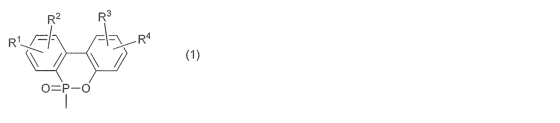
- the compound (A) includes a hydrophobic amide derivative (A1) obtained by reacting an acid anhydride (a1) having a partial structure represented by the following formula (1) with an amine (a2) and an imidized product thereof ( It is at least one compound selected from the group consisting of A2).
- R 1 , R 2 , R 3 and R 4 are each hydrogen or alkyl having 1 to 10 carbon atoms.
- alkyl having 1 to 10 carbon atoms examples include methyl, ethyl, n-propyl, i-propyl, n-butyl, i-butyl, t-butyl, n-pentyl, n-hexyl, n-heptyl, n- Examples include octyl, n-nonyl, and n-decyl.
- Acid anhydride (a1) is not particularly limited as long as it is an acid anhydride having a partial structure of the formula (1).
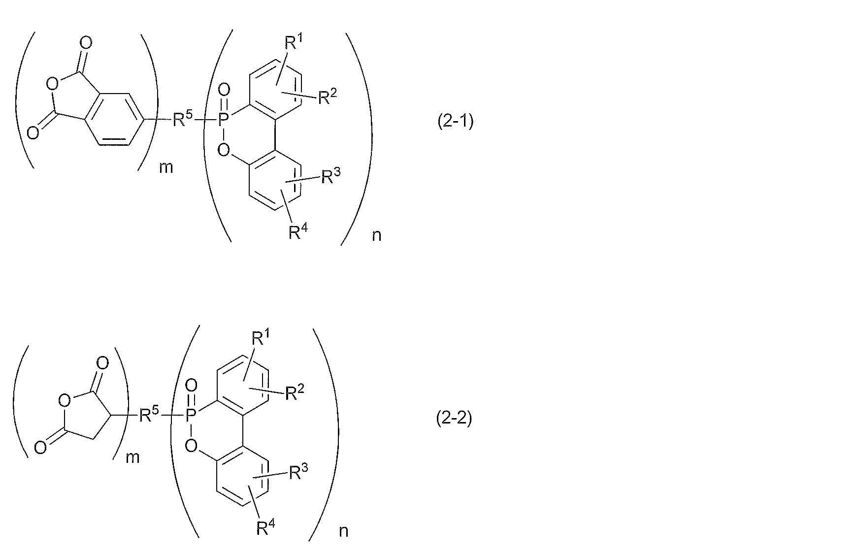
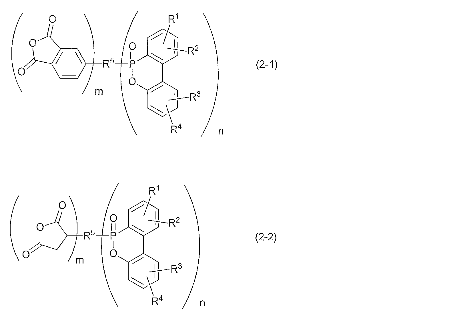
- an acid anhydride represented by the formula (2-1) is more preferable.
- R 1 , R 2 , R 3 and R 4 are each independently hydrogen or alkyl having 1 to 10 carbons, preferably hydrogen or having 1 to 8 carbons Alkyl, more preferably hydrogen, and R 5 is a single bond, carbon or an organic group having 1 to 50 carbon atoms, preferably a single bond, carbon or an organic group having 1 to 30 carbon atoms, more preferably A single bond, carbon or an organic group having 1 to 20 carbon atoms, m is 1 or 2, and n is 1 or 2.
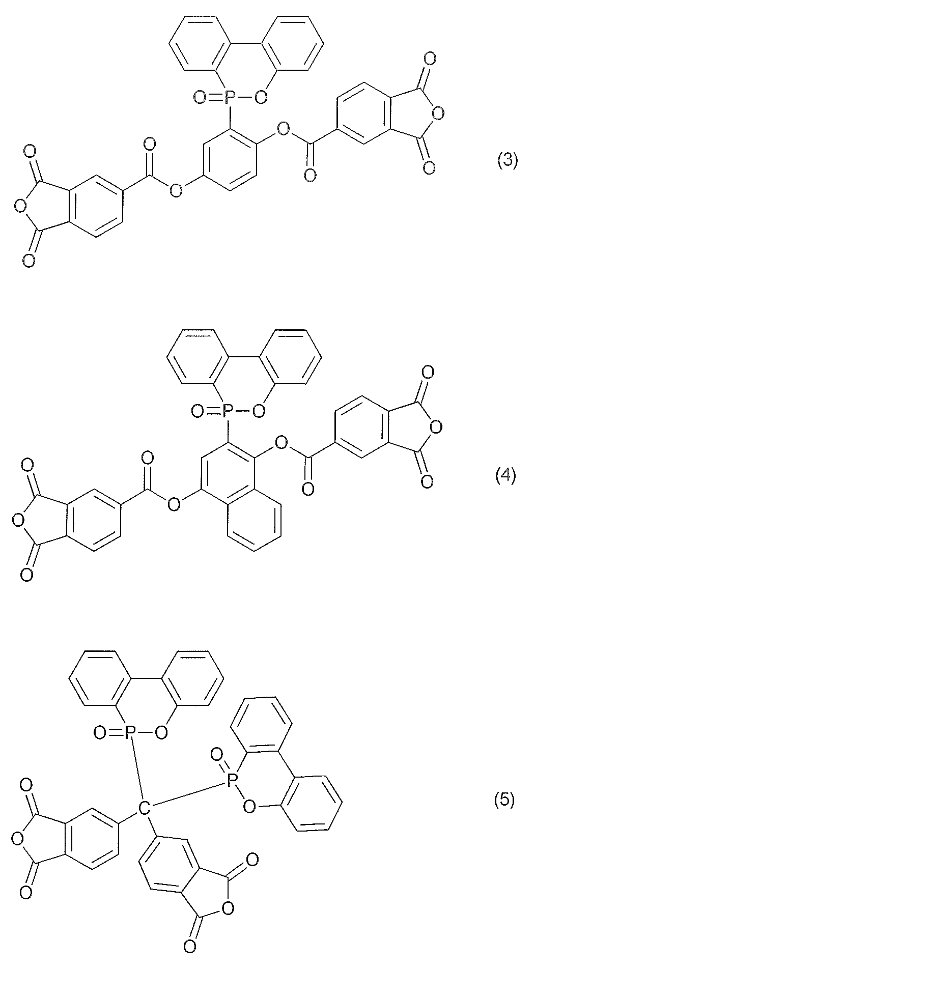
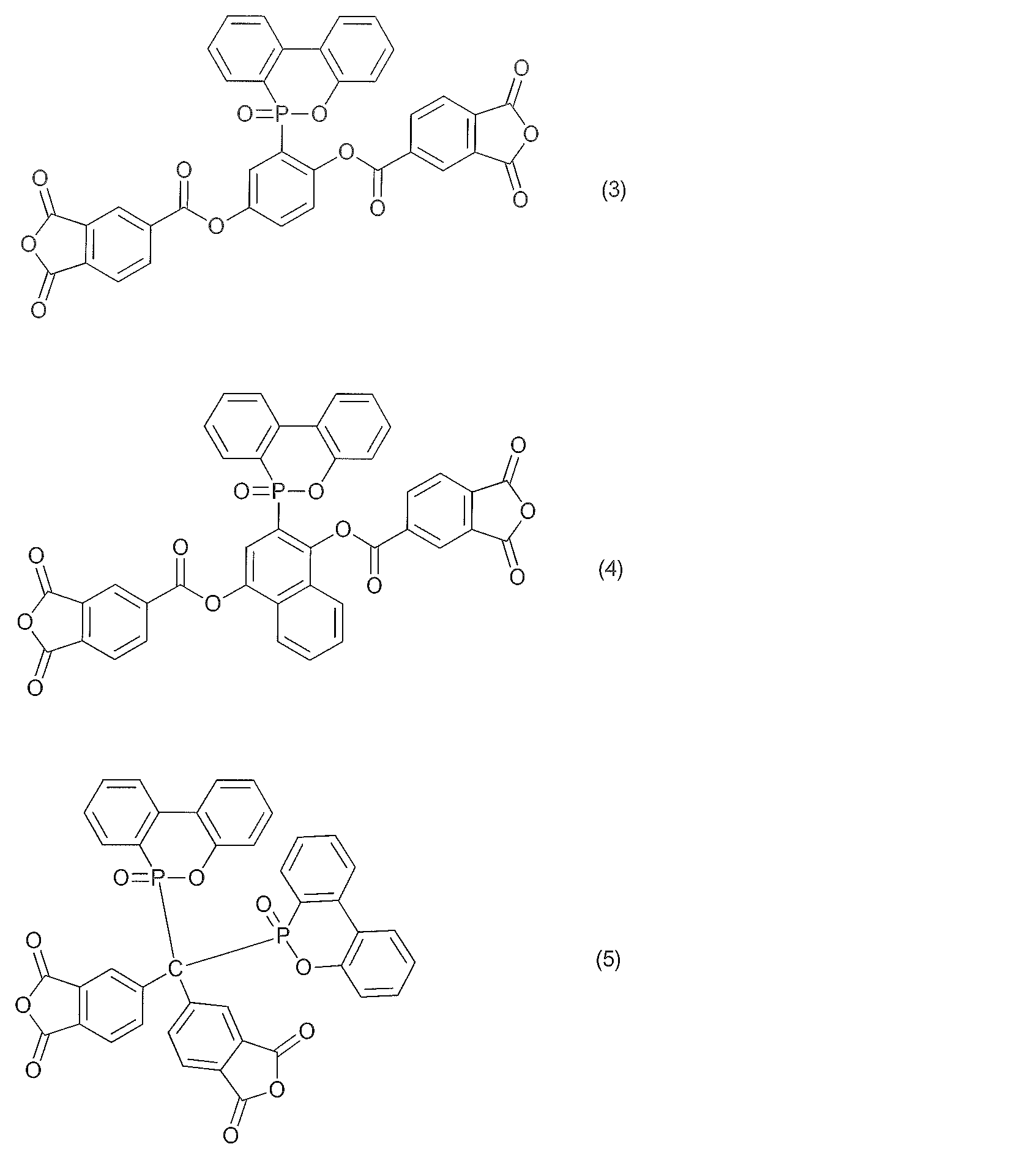
- Preferred examples of the acid anhydride represented by the formula (2-1) include tetracarboxylic dianhydrides represented by the following formulas (3) to (5).
- the amine (a2) is not particularly limited, but a compound represented by the following formula (6) is preferable, and a compound represented by the following formula (7) is more preferable.
- R 6 is a hydrocarbon group having 1 to 50 carbon atoms which may contain a benzene ring or a cyclohexane ring, and at least one hydrogen in the hydrocarbon group is fluorine, chlorine or cyano. It may be replaced.
- T, U and V are each independently a benzene ring or a cyclohexane ring, and at least one hydrogen on these rings is an alkyl having 1 to 3 carbon atoms or an alkyl having 1 to 3 carbon atoms.
- Fluorine-substituted alkyl, fluorine, chlorine or cyano may be substituted
- h is an integer of 0 to 5
- i and j are each an integer of 0 to 2
- R 7 is hydrogen, fluorine, chlorine, cyano
- it is a monovalent organic group having 1 to 30 carbon atoms.
- Examples of the monovalent organic group for R 7 include, for example, alkyl having 1 to 20 carbon atoms, alkenyl having 2 to 20 carbon atoms, alkynyl having 2 to 20 carbon atoms, and carboxylic acid at any site of these organic groups. And an organic group having at least one bond selected from the group consisting of an ester bond, a sulfonate bond, an amide bond, a phosphonic acid bond, an ether bond, a sulfide bond and an imide bond.
- Other raw materials When synthesizing the compound (A), other raw materials may be used in combination with the acid anhydride (a1) and the amine (a2) described above. Examples of other raw materials include tetracarboxylic dianhydrides and diamines that can be used as normal polyimide raw materials, and dicarboxylic anhydrides and monoamines that can be used as normal end-capping agents.
- the compound (A) can be synthesized according to a general method for synthesizing amide derivatives or imides.
- the above-mentioned composition for forming a cured film contains compound (A) with respect to 100 parts by weight of the total amount of the composition. It is contained in an amount of 0.1 to 99.9 parts by weight, preferably 1 to 50 parts by weight, more preferably 1 to 20 parts by weight. When the compound (A) is contained in an amount within the above range, it is possible to form a relatively thin film (film thickness is 1 ⁇ m or less) when forming a cured film.
- the said cured film formation composition may contain a solvent (B) from a viewpoint of adjusting viscosity.
- the viscosity is not particularly limited, but it is important to adjust to a viscosity suitable for the desired printing method.
- the solvent (B) is not particularly limited as long as it can dissolve the compound (A). In addition, even if the solvent alone does not dissolve the compound (A), such a mixed solvent can be used as the solvent (B) as long as the compound (A) can be dissolved by mixing with another solvent. Is possible.
- the solvent (B) include ethanol, benzyl alcohol, cyclohexanol, 1,4-butanediol, glycerin, ethylene glycol, ethylene glycol monomethyl ether, ethylene glycol monobutyl ether, ethylene glycol monophenyl ether, ethylene glycol dimethyl ether, Ethylene glycol monomethyl ether acetate, ethylene glycol monoethyl ether acetate, ethylene glycol monobutyl ether acetate, diethylene glycol, diethylene glycol monomethyl ether, diethylene glycol monoethyl ether, diethylene glycol monopropyl ether, diethylene glycol monobutyl ether, diethylene glycol monophenyl ether, diethyl Glycol dimethyl ether, diethylene glycol diethyl ether, diethylene glycol dibutyl ether, diethylene glycol methyl ethyl ether, diethylene glycol isopropyl methyl ether, diethylene glycol
- ethyl lactate propylene glycol monomethyl ether acetate, methyl 3-methoxypropionate, cyclohexanone, cyclopentanone, diethylene glycol methyl ethyl ether, diethylene glycol monobutyl ether
- Diethylene glycol dimethyl ether and diethylene glycol monobutyl ether acetate are preferably included as the solvent (B).
- amide solvent such as N, N-dimethylformamide and N-methyl- ⁇ -caprolactam is preferably contained in an amount of 50 parts by weight or less with respect to a total of 100 parts by weight of the solvent (B), More preferably, it is contained in an amount of not more than parts, and it is even more preferred that the solvent (B) is a non-amide solvent.
- the reaction solvent when the reaction solvent remains when the synthesis of the compound (A) is completed, the reaction solvent can also be used as the solvent (B).
- a solvent (B) may use only 1 type, or may mix and use 2 or more types.
- the content of the solvent (B) is 0.1 to 99.9% by weight, preferably 50 to 99% by weight, based on the total amount of the composition, from the viewpoint of appropriately adjusting the viscosity of the composition. Preferably, it is 80 to 99% by weight.
- the content of the solvent (B) is within the above range, it is possible to form a relatively thin film (film thickness is 1 ⁇ m or less) when forming a cured film.
- composition for forming a cured film has other components as long as the effects of the present invention are not impaired in order to improve the coating properties and storage stability of the composition, the durability of the resulting cured film, the insulation properties, and the like. (C) can be included.
- components (D) include surfactants, colorants, antistatic agents, coupling agents, pH adjusters, rust preventives, antiseptics, antifungal agents, antioxidants, reduction inhibitors, and evaporation. Accelerators, chelating agents, water-soluble polymers and the like. These components may be a single compound or a mixture of two or more different compounds.
- composition of this invention can be prepared by mixing a compound (A) and the solvent (B) and / or other component (C) as needed by a well-known method.
- the solution obtained by mixing is more preferably degassed after filtration from the viewpoint of preventing impurities from being mixed during coating.
- a fluororesin membrane filter is used for the filtration.
- the cured film of this invention can be formed by apply
- the coating method generally known coating methods such as spin coating, dip coating, slit coating, applicator method, reverse printing method, ink jet printing method, screen printing method, gravure printing method, flexographic printing method, etc. Is mentioned.
- the spin coat method and the slit coat method are preferable because a more uniform film can be formed.
- the heating / drying method is not particularly limited, and a hot plate, a heating oven, or the like can be used.
- a hot plate a heating oven, or the like
- the solvent is effectively evaporated and a film with less surface stickiness can be obtained.
- the heating conditions depend on the material of the substrate, it is preferable to heat at 120 to 400 ° C. for 30 to 240 minutes. Further, depending on the purpose of use, for example, when used as an insulating film, it is preferably cured at a relatively high temperature using an oven. When cured at a temperature range of 180 to 400 ° C. for 30 to 120 minutes, a highly insulating film can be obtained.
- a base material will not be specifically limited if the said composition for cured film formation can be apply
- the shape is not restricted to flat form,
- a curved-surface form may be sufficient.
- the material and form of the substrate are not particularly limited.
- polyester resins such as polyethylene terephthalate, polybutylene terephthalate and polyethylene naphthalate, polyolefin resins such as polyethylene and polypropylene, polyvinyl chloride, fluororesin, Plastic film such as acrylic resin, polyamide, polycarbonate, polyimide; cellophane; acetate; metal foil; laminated film of polyimide and metal foil; glassine paper or parchment paper with sealing effect; polyethylene, clay binder, polyvinyl alcohol, starch And paper treated with carboxymethylcellulose; glass and the like.
- an antioxidant such as a water repellent treatment, a corona treatment, a plasma treatment or a blast treatment as necessary, or an easy adhesion layer or a hard coat is applied to at least a part of the surface A film may be provided.
- an easy adhesion treatment such as a water repellent treatment, a corona treatment, a plasma treatment or a blast treatment as necessary, or an easy adhesion layer or a hard coat is applied to at least a part of the surface A film may be provided.
- the thickness of the substrate is not particularly limited and is appropriately adjusted depending on the purpose of use, but is preferably about 10 ⁇ m to 2 mm, more preferably 20 ⁇ m to 1.5 mm, and further preferably 50 ⁇ m to 1 mm.
- the cured film of the present invention is used as a surface treatment film for forming a lyophobic contrast, if the surface of the substrate is in a lyophilic state, there is no need for pretreatment, but the surface of the substrate is in a lyophobic state. If necessary, before forming the cured film of the present invention, it is desirable to make the substrate lyophilic by a method such as ultraviolet / ozone (UV / O 3 ) cleaning in advance.
- UV / O 3 ultraviolet / ozone
- the surface of the lyophilic substrate has a pure water contact angle at 25 ° C. of preferably 60 degrees or less, more preferably 20 to 55 degrees, and even more preferably 30 to 50 degrees.
- the surface of the cured film of the present invention has a pure water contact angle at 25 ° C. of preferably 80 degrees or more, more preferably 85 to 110 degrees, and still more preferably 90 to 110 degrees.
- the contact angle in this specification measures the value after 1 second of water droplet (pure water) landing at 25 ° C. using “Simage 02B” manufactured by Excimer Co., Ltd.
- the thickness of the cured film of the present invention varies depending on the application of the substrate to be applied, but is preferably 100 nm to 100 ⁇ m, more preferably 200 nm to 50 ⁇ m, and further preferably 500 nm to 10 ⁇ m. Since the film thickness also affects the exposure amount necessary for the ablation process, it is necessary to adjust the film thickness so that the ablation can be performed with the minimum exposure amount.
- the patterned film of the present invention is obtained by laser ablating a part of the cured film of the present invention with a laser beam having a wavelength of 150 to 400 nm.
- a desired pattern film is formed by laser ablating only a predetermined portion on the cured film.
- an interlayer insulating film a through hole for obtaining conduction between layers is obtained.
- an appropriately lyophilic underlayer (substrate) is obtained. Material) can be exposed to form a pattern having an affinity of repellency.
- the difference in the contact angle of pure water at 25 ° C. between the lyophobic part and the lyophilic part is preferably 30 ° or more, more preferably It is 35 to 60 degrees, particularly preferably 40 to 55 degrees. If it is this range, the ink application will be favorable.
- the ink material By applying the ink material only to the entire lyophilic part of such a film or to the whole, the ink material does not remain in the lyophobic part and accumulates in the lyophilic part, so that the ink pattern can be easily formed.
- the film patterned in this manner may be further dried as necessary.
- the apparatus for performing laser ablation processing is not particularly limited as long as it is an apparatus capable of irradiating laser light capable of removing a part of the cured film of the present invention, and a commercially available apparatus can be used.
- An example of such an apparatus is an excimer laser M426 manufactured by Tamarack.
- the wavelength of laser light for laser ablating the cured film is 100 to 450 nm, preferably 150 to 400 nm, and more preferably 200 to 350 nm. It is preferable that the wavelength of the irradiated laser beam be in this range because ablation can be achieved with a low dose.
- the exposure amount of the laser beam necessary for laser ablating the cured film of the present invention is not particularly limited as long as the cured film of the present invention is ablated, but is preferably 500 mJ / cm 2 or less, more preferably 100 to 400 mJ / cm 2 , more preferably 150 to 300 mJ / cm 2 . If laser ablation can be performed with a low exposure amount, the time required for exposure is shortened, and damage to the substrate under the cured film can be suppressed, which is preferable.
- the cured film of the present invention can be used, for example, as an interlayer insulating film on a printed wiring board or a hydrophilic / repellent pattern film for pattern formation on a circuit board.
- a conductive material for obtaining conduction between layers can be embedded in the laser ablated portion. Since the cured film of the present invention has a liquid-repellent surface, it can be easily printed by a general-purpose printing method.
- the conductive material is preferentially printed at a location where the base (base material) previously lyophilicized is exposed.
- the concave portion is formed in the cured film of the present invention by laser ablation, the ink more easily flows into the lyophilic portion.
- the cured film or pattern film of the present invention is used for various laminates, organic thin film transistors, optical components, display elements, and the like.
- PA acid 1 was synthesized in the same manner as in Preparation Example 1 and reacted at 70 ° C. for 3 hours. Then, instead of cooling to room temperature, the heating temperature was increased and water was removed while the reaction temperature was 170 ° C. The reaction was allowed for 5 hours. Thereafter, the mixture was cooled to room temperature to obtain about 110 g of a partially imidized polyamic acid derivative solution having a solid content concentration of 20.0 wt%. The polyamic acid derivative contained in this partially imidized polyamic acid derivative solution is referred to as PA acid 2.
- Product 2 was obtained.
- the viscosity of Composition 2 obtained was 2.5 mPa ⁇ s.
- Product 3 was obtained.
- the viscosity of the obtained composition 3 was 2.0 mPa ⁇ s.
- the lower layer salt was washed with 100 mL of toluene. This washing was performed twice. Moreover, the supernatant liquid which wash
- composition 5 for cured film formation was obtained.
- the viscosity of the obtained composition 5 was 10 mPa ⁇ s.
- Example 1 Corning glass substrate (EAGLE XG: trade name, thickness 0.7 mm) for 3 minutes using a UV / O 3 cleaning device (Takeden UV ozone cleaning reforming device “SKT2005Y-01”) Washed. Next, the cured film-forming composition 1 obtained in Preparation Example 1 was applied to the cleaned glass substrate with a spin coater (“MS-A150” manufactured by Mikasa Co., Ltd.), and then on a hot plate set at 90 ° C. And dried for 3 minutes to obtain a cured film. The film thickness of the obtained cured film was 145 nm.
- the obtained cured film was irradiated with laser light having a wavelength of 248 nm at 140 mJ / cm 2 using an M426 excimer laser system manufactured by Tamarack.
- the pure water contact angle of the laser light irradiated portion was measured and found to be 45 degrees, the same as the contact angle of the glass surface.
- the pure water contact angle of a portion not irradiated with laser light hereinafter referred to as “unirradiated portion” was measured, it was 94 degrees.
- step difference of a laser beam irradiated part and an unirradiated part was measured, it was 142 nm. This value almost coincided with the thickness value 145 nm of the cured film measured in advance.
- the steps were measured at three locations using a step meter P-15 manufactured by KLA Tencor, and the average value was taken as the step. From the results of the pure water contact angle value and the step meter value, it was concluded that ablation occurred due to laser light irradiation and the cured film in the laser light irradiated portion disappeared.
- Example 2 In Example 1, instead of the cured film forming composition 1, a cured film was produced in the same manner as in Example 1 except that the cured film forming composition 2 obtained in Preparation Example 2 was used. Excimer laser irradiation was performed, and the pure water contact angle and film thickness step were measured.
- the pure water contact angle of the laser light irradiated part was 47 degrees, and the pure water contact angle of the unirradiated part was 94 degrees.
- the thickness of the cured film was 152 nm, whereas the step after laser light irradiation was 155 nm.
- Example 3 In Example 1, instead of the cured film forming composition 1, a cured film was produced in the same manner as in Example 1 except that the cured film forming composition 3 obtained in Preparation Example 3 was used. Excimer laser irradiation was performed, and the pure water contact angle and film thickness step were measured.
- the pure water contact angle of the laser light irradiated part was 47 degrees, and the pure water contact angle of the unirradiated part was 93 degrees.
- the thickness of the cured film was 149 nm, whereas the step after laser light irradiation was 148 nm.
- Example 1 In Example 1, instead of the cured film forming composition 1, a cured film was prepared in the same manner as in Example 1 except that the cured film forming composition 4 obtained in Preparation Example 4 was used. Excimer laser irradiation was performed, and the pure water contact angle and film thickness step were measured.
- the pure water contact angle of the laser light irradiated part was 82 degrees, and the pure water contact angle of the unirradiated part was 101 degrees.
- the thickness of the cured film was 75 nm, whereas the step after laser light irradiation was 0 nm, and disappearance of the film due to laser light irradiation could not be confirmed.
- Example 2 In Example 1, instead of the cured film forming composition 1, a cured film was prepared in the same manner as in Example 1 except that the cured film forming composition 5 obtained in Preparation Example 5 was used. Excimer laser irradiation was performed, and the pure water contact angle and film thickness step were measured.
- the pure water contact angle of the laser light irradiated part was 85 degrees, and the pure water contact angle of the unirradiated part was 100 degrees. Moreover, while the film thickness was 560 nm, the level
- the cured film of the example is more efficiently ablated than the cured film of the comparative example, and the pure water contact angle at the ablated part and the pure water contact at the non-ablated part. It is very different from the corner, and a contrast of repellency is formed. Therefore, the cured film of the present invention can be suitably used for interlayer insulating films of printed wiring boards, organic transistors, and the like.
Landscapes
- Physics & Mathematics (AREA)
- Chemical & Material Sciences (AREA)
- General Physics & Mathematics (AREA)
- Health & Medical Sciences (AREA)
- Chemical Kinetics & Catalysis (AREA)
- Medicinal Chemistry (AREA)
- Polymers & Plastics (AREA)
- Organic Chemistry (AREA)
- Optics & Photonics (AREA)
- Macromolecular Compounds Obtained By Forming Nitrogen-Containing Linkages In General (AREA)
Abstract
プリント配線板や半導体パッケージ基板などで必要とされる硬化膜のパターン形成において、レーザーアブレーション法により容易に加工ができる高感度な硬化膜を提供することを課題とする。本発明の硬化膜は、式(1)で表される部分構造を有する酸無水物(a1)とアミン(a2)とを反応させて得られる疎水性アミド誘導体(A1)及びそのイミド化物(A2)からなる群より選ばれる少なくとも一種の化合物(A)を含む組成物から形成され、波長150~400nmのレーザー光でレーザーアブレーション可能である。
Description
本発明は、レーザーアブレーション可能な硬化膜に関し、より具体的には、紫外線を用いたレーザーアブレーション法により容易にパターン膜を形成可能な硬化膜、該硬化膜をアブレーション加工することにより得られるパターン膜、およびそれらの用途に関する。
従来、プリント配線板および半導体パッケージ基板などに使用される絶縁膜のパターン形成としては、感光性樹脂材料を用いたフォトリソ法が主流であった(例えば特許文献1参照)。しかしながら、フォトリソ法では、精細パターン形成には有利であるが、高価な設備が必要となるほか、長く複雑な工程により高い製造コストがかかるという問題がある。
そのため、製造コスト低減のために、インクジェット法をはじめとした数々の印刷手法を利用し、微細な回路パターンを直接描画してプリント配線板などの各種電子部品を形成する手法が注目を浴びている。しかしながら、インクジェット法などの印刷法には、インクの濡れ広がりや液だまりの発生により、フォトリソ法と比較して描画したパターンの精度が低いという問題がある。
これらの問題を解決する方法として、本発明者は、表面にエネルギーを付与することにより表面自由エネルギーを変化させることができる材料を含む層を基板上に形成し、この層にある一定の活性エネルギーを与えることで、微細な配線パターンを描画する前に、予め配線パターンを反映した微細なパターンを持つ撥インク部および親インク部を作成する方法を提案した(特許文献2参照)。
しかしながら、親撥部のコントラストを光照射のみで発現しているため、配線が込み入っている場合や極端に精細なパターンの場合、精度よく描画するためには、しかるべき印刷法にて印刷しなければ、配線間の撥液部を介してインクがブリッジする現象が発現してしまうという問題がある。
なお、フォトリソ法やインクジェット印刷法以外のパターン膜形成方法として、レーザーアブレーション法も考えられるが、現状、レーザーアブレーション法に適した絶縁膜材料は、ほとんど報告されていない。
本発明の課題は、プリント配線板や半導体パッケージ基板などで必要とされる硬化膜のパターン形成において、レーザーアブレーション法により容易に加工ができる高感度な硬化膜を提供することにある。
本発明者は、上記課題を解決するために鋭意検討した結果、特定の構造を有する疎水性アミド誘導体またはそのイミド化物を含む組成物から形成される硬化膜を、波長150~400nmのレーザー光を用いたレーザーアブレーション法により高感度で容易に加工できることを見出し、本発明を完成させた。本発明は、例えば、下記の事項を包含する。
[1] 下記式(1)で表される部分構造を有する酸無水物(a1)とアミン(a2)とを反応させて得られる疎水性アミド誘導体(A1)およびそのイミド化物(A2)からなる群より選ばれる少なくとも一種の化合物(A)を含む組成物から形成される硬化膜であって、波長150~400nmのレーザー光でレーザーアブレーション可能な硬化膜。
[2] 酸無水物(a1)が、下記式(2-1)または(2-2)で表される酸無水物である、項[1]に記載の硬化膜。

[3] 酸無水物(a1)が、下記式(3)~(5)で表されるテトラカルボン酸二無水物からなる群より選ばれる少なくとも1種の化合物を含む、項[1]または[2]に記載の硬化膜。
[4] アミン(a2)が、下記式(6)で表される化合物を含む、項[1]~[3]のいずれか1項に記載の硬化膜。
H2N-R6-NH2 (6)
式中、R6は、ベンゼン環またはシクロヘキサン環を含んでもよい、炭素数1~50の炭化水素基であり、該炭化水素基中の少なくとも1つの水素は、フッ素、塩素またはシアノで置き換えられてもよい。
H2N-R6-NH2 (6)
式中、R6は、ベンゼン環またはシクロヘキサン環を含んでもよい、炭素数1~50の炭化水素基であり、該炭化水素基中の少なくとも1つの水素は、フッ素、塩素またはシアノで置き換えられてもよい。
[5] アミン(a2)が、下記式(7)で表される化合物を含む、項[1]~[4]のいずれか1項に記載の硬化膜。

[6] 25℃における純水の接触角が80度以上の表面を有する、項[1]~[5]のいずれか1項に記載の硬化膜。
[7] 25℃における純水の接触角が60度以下の表面を有する基材上に形成された、項[1]~[6]のいずれか1項に記載の硬化膜。
[7] 25℃における純水の接触角が60度以下の表面を有する基材上に形成された、項[1]~[6]のいずれか1項に記載の硬化膜。
[8] 膜厚が100nm~100μmである、項[1]~[7]のいずれか1項に記載の硬化膜。
[9] 項[1]~[8]のいずれか1項に記載の硬化膜の一部が、波長150~400nmのレーザー光でレーザーアブレーションされたパターン膜。
[9] 項[1]~[8]のいずれか1項に記載の硬化膜の一部が、波長150~400nmのレーザー光でレーザーアブレーションされたパターン膜。
[10] 項[1]~[8]のいずれか1項に記載の硬化膜の一部を、波長150~400nmのレーザー光でレーザーアブレーションする工程を含む、パターン膜の製造方法。
[11] 項[1]~[8]のいずれか1項に記載の硬化膜または項[9]に記載のパターン膜を含む、積層体。
[12] 項[1]~[8]のいずれか1項に記載の硬化膜または項[9]に記載のパターン膜を含む、有機薄膜トランジスタ。
[12] 項[1]~[8]のいずれか1項に記載の硬化膜または項[9]に記載のパターン膜を含む、有機薄膜トランジスタ。
[13] 項[1]~[8]のいずれか1項に記載の硬化膜または項[9]に記載のパターン膜を含む、光学部品。
[14] 項[1]~[8]のいずれか1項に記載の硬化膜または項[9]に記載のパターン膜を含む、表示素子。
[14] 項[1]~[8]のいずれか1項に記載の硬化膜または項[9]に記載のパターン膜を含む、表示素子。
本発明の硬化膜を用いれば、レーザーアブレーション法により容易にパターン形成できるため、工程の簡略化が可能である。また、本発明の硬化膜は高感度であるため、低露光量でのパターン形成が可能である。
また、表面を適切に親液化した基材上に本発明の硬化膜を形成し(形成された硬化膜は撥液部)、該硬化膜のみをアブレーションすることによって(アブレーションされた部分が親液部)、親液部と撥液部のコントラストを形成することができ、また、親液部が凹部となることから、インクが親液部に流れ込みやすくなり、硬化膜表面にインクを塗布する際に容易に塗り分けが可能となる。
以下、本発明に係る硬化膜、パターン膜およびそれらの用途について詳細に説明する。
[硬化膜]
本発明の硬化膜は、後述する化合物(A)を含む組成物(以下「硬化膜形成用組成物」ともいう。)から形成され、波長150~400nmのレーザー光でレーザーアブレーション可能な硬化膜である。
[硬化膜]
本発明の硬化膜は、後述する化合物(A)を含む組成物(以下「硬化膜形成用組成物」ともいう。)から形成され、波長150~400nmのレーザー光でレーザーアブレーション可能な硬化膜である。
<化合物(A)>
上記化合物(A)は、下記式(1)で表される部分構造を有する酸無水物(a1)とアミン(a2)とを反応させて得られる疎水性アミド誘導体(A1)およびそのイミド化物(A2)からなる群より選ばれる少なくとも一種の化合物である。
上記化合物(A)は、下記式(1)で表される部分構造を有する酸無水物(a1)とアミン(a2)とを反応させて得られる疎水性アミド誘導体(A1)およびそのイミド化物(A2)からなる群より選ばれる少なくとも一種の化合物である。

炭素数1~10のアルキルとしては、例えば、メチル、エチル、n-プロピル、i-プロピル、n-ブチル、i-ブチル、t-ブチル、n-ペンチル、n-ヘキシル、n-ヘプチル、n-オクチル、n-ノニル、n-デシルが挙げられる。
1.酸無水物(a1)
酸無水物(a1)としては、式(1)の部分構造を有する酸無水物であれば特に限定されないが、例えば、下記式(2-1)または(2-2)で表される酸無水物が好ましく、式(2-1)で表われる酸無水物がより好ましい。
酸無水物(a1)としては、式(1)の部分構造を有する酸無水物であれば特に限定されないが、例えば、下記式(2-1)または(2-2)で表される酸無水物が好ましく、式(2-1)で表われる酸無水物がより好ましい。
式(2-1)で表される酸無水物の好ましい例として、下記式(3)~(5)で表されるテトラカルボン酸二無水物が挙げられる。
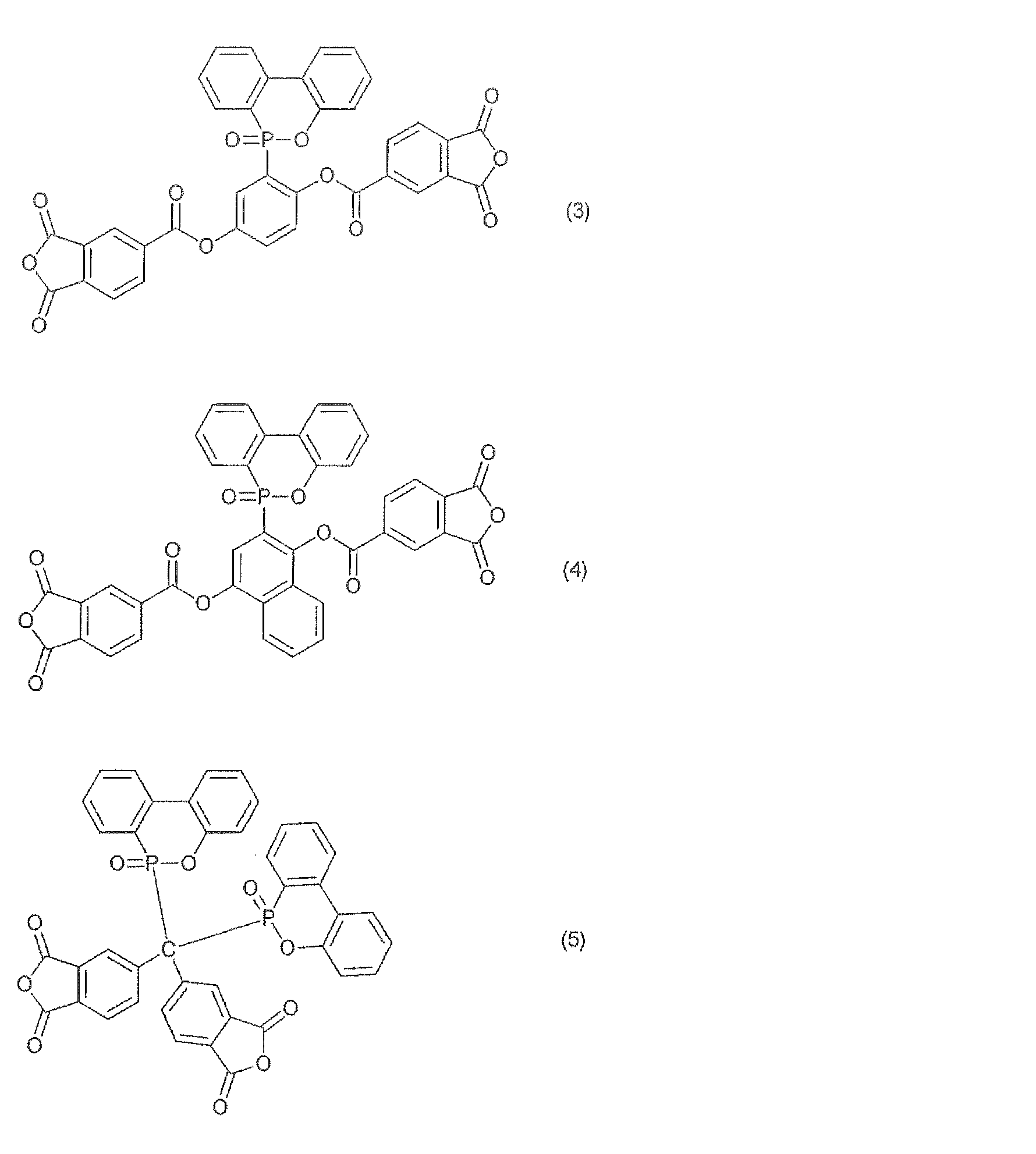
2.アミン(a2)
アミン(a2)は、特に限定されないが、下記式(6)で表される化合物が好ましく、下記式(7)で表わされる化合物がより好ましい。
H2N-R6-NH2 (6)
式(6)中、R6は、ベンゼン環またはシクロヘキサン環を含んでもよい、炭素数1~50の炭化水素基であり、該炭化水素基中の少なくとも1つの水素は、フッ素、塩素またはシアノで置き換えられてもよい。
アミン(a2)は、特に限定されないが、下記式(6)で表される化合物が好ましく、下記式(7)で表わされる化合物がより好ましい。
H2N-R6-NH2 (6)
式(6)中、R6は、ベンゼン環またはシクロヘキサン環を含んでもよい、炭素数1~50の炭化水素基であり、該炭化水素基中の少なくとも1つの水素は、フッ素、塩素またはシアノで置き換えられてもよい。

R7における1価の有機基としては、例えば、炭素数1~20のアルキル、炭素数2~20のアルケニル、炭素素2~20のアルキニル、ならびにこれらの有機基の任意の部位に、カルボン酸エステル結合、スルホン酸エステル結合、アミド結合、ホスホン酸結合、エーテル結合、スルフィド結合およびイミド結合からなる群より選ばれる少なくとも1つの結合を有する有機基などが挙げられる。
式(7)で表わされる化合物の好ましい態様としては、下記式(8)で表されるジアミンが挙げられる。

3.他の原料
化合物(A)を合成する際に、上述した酸無水物(a1)およびアミン(a2)とともに、他の原料を併用してもよい。他の原料としては、通常のポリイミドの原料として使用できるテトラカルボン酸二無水物やジアミン、ならびに、通常の末端封止剤として使用できるジカルボン酸無水物やモノアミンなどが挙げられる。
化合物(A)を合成する際に、上述した酸無水物(a1)およびアミン(a2)とともに、他の原料を併用してもよい。他の原料としては、通常のポリイミドの原料として使用できるテトラカルボン酸二無水物やジアミン、ならびに、通常の末端封止剤として使用できるジカルボン酸無水物やモノアミンなどが挙げられる。
4.化合物(A)の合成方法
上記化合物(A)は、一般的なアミド誘導体またはイミドの合成法に従って合成することができる。
上記化合物(A)は、一般的なアミド誘導体またはイミドの合成法に従って合成することができる。
5.化合物(A)の含有量
上記硬化膜形成用組成物は、硬化膜を得る観点および組成物の粘度を適切に調整する観点から、組成物の総量100重量部に対して、化合物(A)を0.1~99.9重量部、好ましくは1~50重量部、より好ましくは1~20重量部の量で含む。前記範囲の量で化合物(A)を含むと、硬化膜の製膜時、比較的薄い膜(膜厚が1μm以下)を形成することが可能である。
上記硬化膜形成用組成物は、硬化膜を得る観点および組成物の粘度を適切に調整する観点から、組成物の総量100重量部に対して、化合物(A)を0.1~99.9重量部、好ましくは1~50重量部、より好ましくは1~20重量部の量で含む。前記範囲の量で化合物(A)を含むと、硬化膜の製膜時、比較的薄い膜(膜厚が1μm以下)を形成することが可能である。
<溶媒(B)>
上記硬化膜形成用組成物は、粘度調整を行う観点から、溶媒(B)を含有してもよい。粘度は特に制限されないが、所望する印刷方法に適した粘度に調整することが重要である。
上記硬化膜形成用組成物は、粘度調整を行う観点から、溶媒(B)を含有してもよい。粘度は特に制限されないが、所望する印刷方法に適した粘度に調整することが重要である。
溶媒(B)は、化合物(A)を溶解することができる溶媒であれば、特に制限されない。また、単独では化合物(A)を溶解しない溶媒であっても、他の溶媒と混合することによって化合物(A)を溶解できるのであれば、そのような混合溶媒を、溶媒(B)として用いることが可能である。
溶媒(B)の具体例としては、エタノール、ベンジルアルコール、シクロヘキサノール、1,4-ブタンジオール、グリセリン、エチレングリコール、エチレングリコールモノメチルエーテル、エチレングリコールモノブチルエーテル、エチレングリコールモノフェニルエーテル、エチレングリコールジメチルエーテル、エチレングリコールモノメチルエーテルアセテート、エチレングリコールモノエチルエーテルアセテート、エチレングリコールモノブチルエーテルアセテート、ジエチレングリコール、ジエチレングリコールモノメチルエーテル、ジエチレングリコールモノエチルエーテル、ジエチレングリコールモノプロピルエーテル、ジエチレングリコールモノブチルエーテル、ジエチレングリコールモノフェニルエーテル、ジエチレングリコールジメチルエーテル、ジエチレングリコールジエチルエーテル、ジエチレングリコールジブチルエーテル、ジエチレングリコールメチルエチルエーテル、ジエチレングリコールイソプロピルメチルエーテル、ジエチレングリコールブチルメチルエーテル、ジエチレングリコールモノメチルエーテルアセテート、ジエチレングリコールモノエチルエーテルアセテート、ジエチレングリコールモノブチルエーテルアセテート、トリエチレングリコールモノメチルエーテル、トリエチレングリコールジメチルエーテル、トリエチレングリコールジビニルエーテル、プロピレングリコール、プロピレングリコールモノメチルエーテル、プロピレングリコールモノエチルエーテル、プロピレングリコールモノブチルエーテル、プロピレングリコールモノフェニルエーテル、プロピレングリコールジメチルエーテル、プロピレングリコールモノメチルエーテルアセテート、プロピレングリコールモノエチルエーテルアセテート、プロピレングリコールモノプロピルエーテルアセテート、ジプロピレングリコール、ジプロピレングリコールモノメチルエーテル、ジプロピレングリコールジメチルエーテル、ジプロピレングリコールモノエチルエーテル、ジプロピレングリコールモノプロピルエーテル、ジプロピレングリコールモノブチルエーテル、ジプロピレングリコールモノフェニルエーテル、ジプロピレングリコールモノメチルエーテルアセテート、ジプロピレングリコールモノエチルエーテルアセテート、ジプロピレングリコールモノブチルエーテルアセテート、トリエチレングリコール、トリプロピレングリコール、トリプロピレングリコールメチルエーテル、トリプロピレングリコールモノブチルエーテル、トリプロピレングリコールモノメチルエーテル、トリプロピレングリコールジメチルエーテル、テトラメチレングリコールモノビニルエーテル、3-メトキシプロピオン酸メチル、3-エトキシプロピオン酸エチル、3-メトキシブタノール、3-メトキシブチルアセテート、2-ヒドロキシイソ酪酸メチル、2-ヒドロキシイソ酪酸i-プロピル、2-ヒドロキシイソ酪酸i-ブチル、2-ヒドロキシイソ酪酸n-ブチル、酢酸ブチル、プロピオン酸ブチル、メトキシ酢酸メチル、メトキシ酢酸エチル、メトキシ酢酸ブチル、エトキシ酢酸メチル、エトキシ酢酸エチル、3-メトキシプロピオン酸エチル、アセト酢酸メチル、アセト酢酸エチル、乳酸エチル、ピルビン酸メチル、ピルビン酸エチル、ピルビン酸プロピル、安息香酸メチル、安息香酸エチル、ジオキサン、トルエン、キシレン、アニソール、シクロヘキサノン、シクロペンタノン、γ-ブチロラクトン、1,3-ジオキソラン、1,4-ジオキサン、2-ピロリドン、1-メチル-2-ピロリドン(略語:NMP)、1-ビニル-2-ピロリドン、1-ブチル-2-ピロリドン、1-エチル-2-ピロリドン、1-(2-ヒドロキシエチル)-2-ピロリドン、1-アセチル-2-ピロリドン、N-メチル-ε-カプロラクタム、N,N-ジメチルアセトアミド、N,N-ジエチルアセトアミド、N,N-ジメチルプロピオンアミド、N,N-ジメチルホルムアミドおよび1,3-ジメチル-2-イミダゾリジノンが挙げられる。
これらの中では、化合物(A)の溶解性および製膜性の観点から、乳酸エチル、プロピレングリコールモノメチルエーテルアセテート、3-メトキシプロピオン酸メチル、シクロヘキサノン、シクロペンタノン、ジエチレングリコールメチルエチルエーテル、ジエチレングリコールモノブチルエーテル、ジエチレングリコールジメチルエーテル、ジエチレングリコールモノブチルエーテルアセテートを、溶媒(B)として含むことが好ましい。
なお、上記の例示溶媒の中では、製膜性の点から、1-ビニル-2-ピロリドン、1-ブチル-2-ピロリドン、1-エチル-2-ピロリドン、1-(2-ヒドロキシエチル)-2-ピロリドン、2-ピロリドン、1-メチル-2-ピロリドン(略語:NMP)、1-アセチル-2-ピロリドン、N,N-ジメチルアセトアミド、N,N-ジエチルアセトアミド、N,N-ジメチルプロピオンアミド、N,N-ジメチルホルムアミド、N-メチル-ε-カプロラクタムなどのアミド系溶媒は、溶媒(B)の合計100重量部に対して、50重量部以下の量で含まれることが好ましく、20重量部以下の量で含まれることがより好ましく、全く含まれない、すなわち溶媒(B)が非アミド系の溶媒であることがさらに好ましい。
また、化合物(A)の合成が完了したときに反応溶媒が残存している場合、その反応溶媒を溶媒(B)として使用することもできる。
溶媒(B)は、1種のみを用いてもよく、または、2種以上を混合して用いてもよい。また、溶媒(B)の含有量は、組成物の粘度を適切に調整する観点から、組成物の総量に対して、0.1~99.9重量%、好ましくは50~99重量%、より好ましくは80~99重量%である。溶媒(B)の含有量が前記範囲内であると、硬化膜の製膜時、比較的薄い膜(膜厚が1μm以下)を形成することが可能である。
溶媒(B)は、1種のみを用いてもよく、または、2種以上を混合して用いてもよい。また、溶媒(B)の含有量は、組成物の粘度を適切に調整する観点から、組成物の総量に対して、0.1~99.9重量%、好ましくは50~99重量%、より好ましくは80~99重量%である。溶媒(B)の含有量が前記範囲内であると、硬化膜の製膜時、比較的薄い膜(膜厚が1μm以下)を形成することが可能である。
<その他の成分(C)>
上記硬化膜形成用組成物は、組成物の塗布特性および保存安定性や、得られる硬化膜の耐久性、絶縁性等の向上のために、本発明の効果を損なわない範囲において、その他の成分(C)を含むことができる。
上記硬化膜形成用組成物は、組成物の塗布特性および保存安定性や、得られる硬化膜の耐久性、絶縁性等の向上のために、本発明の効果を損なわない範囲において、その他の成分(C)を含むことができる。
その他の成分(D)としては、例えば、界面活性剤、着色剤、帯電防止剤、カップリング剤、pH調整剤、防錆剤、防腐剤、防黴剤、酸化防止剤、還元防止剤、蒸発促進剤、キレート化剤、水溶性ポリマーなどが挙げられる。これらの成分は1種の化合物であっても、2種以上の異なる化合物の混合物であってもよい。
<硬化膜形成用組成物の調製>
本発明の組成物は、化合物(A)ならびに必要に応じて溶媒(B)および/またはその他の成分(C)を公知の方法により混合することで調製することができる。混合して得られた溶液は、塗布の際の不純物混入を防ぐ観点から、ろ過した後、脱気することがより好ましい。前記ろ過には、例えばフッ素樹脂製のメンブレンフィルターなどが用いられる。
本発明の組成物は、化合物(A)ならびに必要に応じて溶媒(B)および/またはその他の成分(C)を公知の方法により混合することで調製することができる。混合して得られた溶液は、塗布の際の不純物混入を防ぐ観点から、ろ過した後、脱気することがより好ましい。前記ろ過には、例えばフッ素樹脂製のメンブレンフィルターなどが用いられる。
<硬化膜の形成方法>
本発明の硬化膜は、上記硬化膜形成用組成物を基材に塗布して加熱・乾燥等することにより形成することができる。
本発明の硬化膜は、上記硬化膜形成用組成物を基材に塗布して加熱・乾燥等することにより形成することができる。
塗布方法としては、一般的に知られている塗布方法、例えば、スピンコート、ディップコート、スリットコート法、アプリケーター法、反転印刷法、インクジェット印刷法、スクリーン印刷法、グラビア印刷法、フレキソ印刷法などが挙げられる。なかでもスピンコート法およびスリットコート法は、より均一な膜を形成できることから好ましい。
加熱・乾燥方法は特に限定されないが、ホットプレート、加熱オーブン等を用いることができる。また、50~120℃の温度範囲で1~30分乾燥させると、溶媒が効果的に蒸発し、表面のべたつきが少ない膜を得ることができる。
また、必要に応じて乾燥後にさらに加熱・焼成してもよい。加熱条件は基材の材質にもよるが、120~400℃で30~240分間、加熱することが好ましい。また、使用目的に応じて、例えば絶縁膜として使用する場合、オーブンを用いて比較的高温で硬化させることが好ましい。180~400℃の温度範囲で、30~120分間硬化させると、絶縁性が高い膜を得ることができる。
基材は、上記硬化膜形成用組成物が塗布される対象となり得るものであれば、特に限定されず、その形状は平板状に限られず、曲面状であってもよい。
また、基材の材質および形態は特に限定されないが、例えば、ポリエチレンテレフタラート、ポリブチレンテレフタラート、ポリエチレンナフタレート等のポリエステル系樹脂、ポリエチレン、ポリプロピレン等のポリオレフィン系樹脂、ポリ塩化ビニル、フッ素樹脂、アクリル系樹脂、ポリアミド、ポリカーボネート、ポリイミドなどのプラスチックフィルム;セロハン;アセテート;金属箔;ポリイミドと金属箔との積層フィルム;目止め効果があるグラシン紙またはパーチメント紙;ポリエチレン、クレーバインダー、ポリビニルアルコール、でんぷん、カルボキシルメチルセルロースなどで目止め処理した紙;ガラスなどを挙げることができる。
また、基材の材質および形態は特に限定されないが、例えば、ポリエチレンテレフタラート、ポリブチレンテレフタラート、ポリエチレンナフタレート等のポリエステル系樹脂、ポリエチレン、ポリプロピレン等のポリオレフィン系樹脂、ポリ塩化ビニル、フッ素樹脂、アクリル系樹脂、ポリアミド、ポリカーボネート、ポリイミドなどのプラスチックフィルム;セロハン;アセテート;金属箔;ポリイミドと金属箔との積層フィルム;目止め効果があるグラシン紙またはパーチメント紙;ポリエチレン、クレーバインダー、ポリビニルアルコール、でんぷん、カルボキシルメチルセルロースなどで目止め処理した紙;ガラスなどを挙げることができる。
なお、これらの基材を構成する物質には、本発明の効果に悪影響を及ぼさない範囲において、酸化防止剤、劣化防止剤、充填剤、紫外線吸収剤、帯電防止剤および電波防止剤等の添加剤が含まれていてもよい。また、基材の表面の少なくとも一部には、必要に応じて撥水処理、コロナ処理、プラズマ処理またはブラスト処理などの易接着処理を施したり、表面の少なくとも一部に易接着層やハードコート膜を設けたりしてもよい。
基材の厚さは、特に限定されず、使用する目的により適宜調整されるが、好ましくは10μm~2mm程度であり、より好ましくは20μm~1.5mm、さらに好ましくは50μm~1mmである。
本発明の硬化膜を、親撥コントラストを形成する表面処理膜として使用する場合、基材の表面が親液状態であれば特に前処理する必要はないが、基材の表面が撥液状態であれば、必要に応じて、本発明の硬化膜を形成する前に基材を予め紫外線/オゾン(UV/O3)洗浄する方法等により親液化することが望ましい。
親液化された基材の表面は、25℃における純水の接触角が、好ましくは60度以下、より好ましくは20~55度、さらに好ましくは30~50度である。
本発明の硬化膜の表面は、25℃における純水の接触角が、好ましくは80度以上、より好ましくは85~110度、さらに好ましくは90~110度である。
本発明の硬化膜の表面は、25℃における純水の接触角が、好ましくは80度以上、より好ましくは85~110度、さらに好ましくは90~110度である。
なお、本明細書における接触角は、(株)エキシマ製「SImage 02B」を用いて、25℃における水滴(純水)着弾1秒後の値を計測したものである。
本発明の硬化膜の膜厚は、塗布する基材の用途により異なるが、好ましくは100nm~100μm、より好ましくは200nm~50μm、さらに好ましくは500nm~10μmである。なお、膜厚は、アブレーション処理に必要な露光量にも影響するため、必要最低限の露光量でアブレーションできるよう、調整する必要がある。
本発明の硬化膜の膜厚は、塗布する基材の用途により異なるが、好ましくは100nm~100μm、より好ましくは200nm~50μm、さらに好ましくは500nm~10μmである。なお、膜厚は、アブレーション処理に必要な露光量にも影響するため、必要最低限の露光量でアブレーションできるよう、調整する必要がある。
[パターン膜]
本発明のパターン膜は、本発明の硬化膜の一部が、波長150~400nmのレーザー光でレーザーアブレーションされたものである。このように硬化膜上の所定の箇所のみをレーザーアブレーションすることにより、所望のパターン膜が形成される。層間絶縁膜の場合には層間の導通を得るためのスルーホールが得られ、親撥パターニングの場合は、本発明の硬化膜の一部を除去することで、適切に親液化された下地(基材)を露出させ、親撥コントラストをもつパターンを形成できる。
本発明のパターン膜は、本発明の硬化膜の一部が、波長150~400nmのレーザー光でレーザーアブレーションされたものである。このように硬化膜上の所定の箇所のみをレーザーアブレーションすることにより、所望のパターン膜が形成される。層間絶縁膜の場合には層間の導通を得るためのスルーホールが得られ、親撥パターニングの場合は、本発明の硬化膜の一部を除去することで、適切に親液化された下地(基材)を露出させ、親撥コントラストをもつパターンを形成できる。
親撥パターン膜の場合、撥液部と親液部における25℃での純水の接触角の差(以下「接触角差」ともいう。)は、好ましくは30度以上であり、より好ましくは35~60度であり、特に好ましくは40~55度である。この範囲であれば、インクの塗りわけが良好である。なお、接触角差は下記式:
式(e);接触角差(度)=撥液部の接触角(度)-親液部の接触角(度)
により求められる。
式(e);接触角差(度)=撥液部の接触角(度)-親液部の接触角(度)
により求められる。
このような膜の親液部のみ、または全体にインク材料を塗布することにより、インク材料が撥液部には残らず、親液部に集積するため、インクのパターン形成が容易となる。このようにしてパターン形成された膜は、必要に応じてさらに乾燥してもよい。
レーザーアブレーション処理をするための装置は、本発明の硬化膜の一部を除去できるレーザー光を照射できる装置であれば特に限定されず、市販の装置を使用できる。そのような装置としては、例えばTamarack社製エキシマレーザーM426が挙げられる。
<照射波長>
本硬化膜をレーザーアブレーションするためのレーザー光の波長は、100~450nm、好ましくは150~400nm、より好ましくは200~350nmである。照射されるレーザー光の波長がこの範囲にあると、低照射量でアブレーション可能となるので好ましい。
本硬化膜をレーザーアブレーションするためのレーザー光の波長は、100~450nm、好ましくは150~400nm、より好ましくは200~350nmである。照射されるレーザー光の波長がこの範囲にあると、低照射量でアブレーション可能となるので好ましい。
<露光照射量>
本発明の硬化膜をレーザーアブレーションするのに必要なレーザー光の露光量は、本発明の硬化膜がアブレーションされる露光量であれば特に限定されないが、好ましくは500mJ/cm2以下、より好ましくは100~400mJ/cm2、さらに好ましくは150~300mJ/cm2である。低い露光量でレーザーアブレーションできれば、露光に必要な時間も短くなり、また、硬化膜の下にある基材へのダメージも抑制できるため好ましい。
本発明の硬化膜をレーザーアブレーションするのに必要なレーザー光の露光量は、本発明の硬化膜がアブレーションされる露光量であれば特に限定されないが、好ましくは500mJ/cm2以下、より好ましくは100~400mJ/cm2、さらに好ましくは150~300mJ/cm2である。低い露光量でレーザーアブレーションできれば、露光に必要な時間も短くなり、また、硬化膜の下にある基材へのダメージも抑制できるため好ましい。
[用途]
本発明の硬化膜は、例えばプリント配線板における層間絶縁膜や、回路基板におけるパターン形成のための親撥パターン膜として利用できる。
本発明の硬化膜は、例えばプリント配線板における層間絶縁膜や、回路基板におけるパターン形成のための親撥パターン膜として利用できる。
層間絶縁膜では、レーザーアブレーションされた箇所に、層間の導通を得るための導電材料を埋め込むことができる。本発明の硬化膜は、表面が撥液化された膜となるため、汎用の印刷法で容易に印刷可能である。
親撥パターン膜では、予め親液化した下地(基材)が露出している箇所に優先的に導電材料が印刷される。また、レーザーアブレーションにより本発明の硬化膜に凹部が形成されるため、より親液部へインクが流れ込みやすくなる。
本発明の硬化膜またはパターン膜は、各種積層体、有機薄膜トランジスタ、光学部品、表示素子などに用いられる。
以下、実施例に基づいて本発明をより具体的に説明するが、本発明はこれら実施例に何ら限定されるものではない。
<試薬>
下記調製例で用いた試薬は以下のとおりである。
TAPQ;上記式(3)で表わされるテトラカルボン酸二無水物(マナック(株)製)
BAPP;2,2-ビス[4-(4-アミノフェノキシ)フェニル]プロパン(和歌山精化工業(株)製)
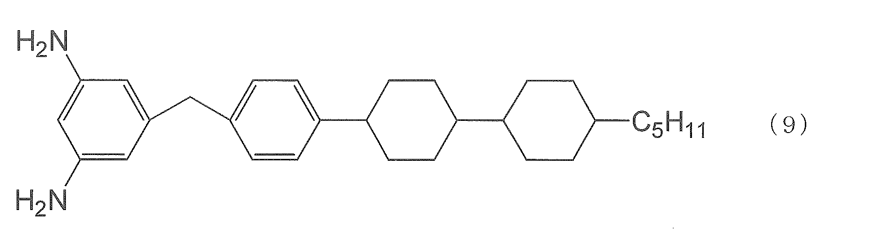
DA5HP;下記式(9)で表わされる5-((4-(4-(4-ペンチルシクロヘキシル)シクロヘキシル)フェニル)メチル)-1,3-ジアミノベンゼン
なお、DA5HPは特開2002-162630号公報に記載の合成法により合成した。
<試薬>
下記調製例で用いた試薬は以下のとおりである。
TAPQ;上記式(3)で表わされるテトラカルボン酸二無水物(マナック(株)製)
BAPP;2,2-ビス[4-(4-アミノフェノキシ)フェニル]プロパン(和歌山精化工業(株)製)
DA5HP;下記式(9)で表わされる5-((4-(4-(4-ペンチルシクロヘキシル)シクロヘキシル)フェニル)メチル)-1,3-ジアミノベンゼン
なお、DA5HPは特開2002-162630号公報に記載の合成法により合成した。
<調製例1>
温度計、攪拌機、原料投入仕込み口及び窒素ガス導入口を備えた500mLの四つ口フラスコに6.6484g(0.01536モル)のDA5HP、2.052g(0.00512モル)のBAPP及び87.91gの脱水NMPを入れ、乾燥窒素雰囲気で攪拌して溶解した。反応系の温度を5~70℃の範囲内に保ちながら13.442g(0.02048モル)のTAPQを添加し、さらに70℃で3時間反応させた。その後、室温に冷却し、固形分濃度が20.0wt%のポリアミド酸誘導体溶液約110gを得た。このポリアミド酸誘導体溶液に含まれるポリアミド酸をPA酸1と称する。
温度計、攪拌機、原料投入仕込み口及び窒素ガス導入口を備えた500mLの四つ口フラスコに6.6484g(0.01536モル)のDA5HP、2.052g(0.00512モル)のBAPP及び87.91gの脱水NMPを入れ、乾燥窒素雰囲気で攪拌して溶解した。反応系の温度を5~70℃の範囲内に保ちながら13.442g(0.02048モル)のTAPQを添加し、さらに70℃で3時間反応させた。その後、室温に冷却し、固形分濃度が20.0wt%のポリアミド酸誘導体溶液約110gを得た。このポリアミド酸誘導体溶液に含まれるポリアミド酸をPA酸1と称する。
得られたPA酸1のNMP溶液(固形分20.0wt%)1.0gおよびシクロペンタノン3gを混合溶解した後、フッ素樹脂製のメンブレンフィルター(0.5μm)でろ過することにより、硬化膜形成用組成物1を得た。得られた組成物1の粘度は2.2mPa・sであった。
<調製例2>
調製例1と同様の方法でPA酸1の合成を行い、70℃で3時間反応させた後、室温に冷却するかわりに、加熱温度を上げ、水を除去しながら、さらに反応温度170℃で5時間反応させた。その後、室温に冷却し、固形分濃度が20.0wt%の部分イミド化したポリアミド酸誘導体溶液約110gを得た。この部分イミド化したポリアミド酸誘導体溶液に含まれるポリアミド酸誘導体をPA酸2と称する。
調製例1と同様の方法でPA酸1の合成を行い、70℃で3時間反応させた後、室温に冷却するかわりに、加熱温度を上げ、水を除去しながら、さらに反応温度170℃で5時間反応させた。その後、室温に冷却し、固形分濃度が20.0wt%の部分イミド化したポリアミド酸誘導体溶液約110gを得た。この部分イミド化したポリアミド酸誘導体溶液に含まれるポリアミド酸誘導体をPA酸2と称する。
PA酸1のNMP溶液(固形分20.0wt%)の代わりにPA酸2のNMP溶液(固形分20.0wt%)を使用したこと以外は、調製例1と同様にして硬化膜形成用組成物2を得た。得られた組成物2の粘度は2.5mPa・sであった。
<調製例3>
温度計、攪拌機、原料投入仕込み口及び窒素ガス導入口を備えた500mLの四つ口フラスコに8.648g(0.02048モル)のDA5HP及び87.91gの脱水NMPを入れ、乾燥窒素雰囲気で攪拌して溶解した。反応系の温度を5~70℃の範囲内に保ちながら13.442g(0.02048モル)のTAPQを添加し、さらに70℃で3時間反応させた。その後、室温に冷却し、固形分濃度が20.0wt%のポリアミド酸誘導体溶液約110gを得た。このポリアミド酸誘導体溶液に含まれるポリアミド酸誘導体をPA酸3と称する。
温度計、攪拌機、原料投入仕込み口及び窒素ガス導入口を備えた500mLの四つ口フラスコに8.648g(0.02048モル)のDA5HP及び87.91gの脱水NMPを入れ、乾燥窒素雰囲気で攪拌して溶解した。反応系の温度を5~70℃の範囲内に保ちながら13.442g(0.02048モル)のTAPQを添加し、さらに70℃で3時間反応させた。その後、室温に冷却し、固形分濃度が20.0wt%のポリアミド酸誘導体溶液約110gを得た。このポリアミド酸誘導体溶液に含まれるポリアミド酸誘導体をPA酸3と称する。
PA酸1のNMP溶液(固形分20.0wt%)の代わりにPA酸3のNMP溶液(固形分20.0wt%)を使用したこと以外は、調製例1と同様にして硬化膜形成用組成物3を得た。得られた組成物3の粘度は2.0mPa・sであった。
<調製例4>
特開2011-57963号公報の実施例1に記載された調製法に従って、硬化膜形成用組成物4を得た。
特開2011-57963号公報の実施例1に記載された調製法に従って、硬化膜形成用組成物4を得た。
<調製例5>
1Lの四つ口フラスコにトルエン200mLを投入し、トリエチルアミン38.45g(0.38mol)を加え、攪拌しながらメタンスルホン酸37.44g(0.39mol)をゆっくり滴下した。室温下で30分間攪拌した後、無水マレイン酸25.90g(0.26mol)を加え、ダイマージアミンであるCRODA社製「プリアミン 1074」(商品名)56.98g(0.11mol)をゆっくり滴下した。室温下で30分間攪拌した後、加熱してトルエン還流をしながら、水分留器で反応中に生成した水を分離させた。8時間毎に、一旦40℃まで冷却し、メタンスルホン酸5.00g(0.05mol)を追加投入した後、再び加温してトルエン還流をしながら、水の除去を行った。取得した水の量が理論値3.96gに達した後、加温を止め、液温が40℃以下になるまで冷却した。次いで、反応液にトルエン100mLを投入し、室温で10~15分間攪拌後、終夜放置し、塩と生成物を分液させた。下層の塩を100mLのトルエンにて洗浄した。この洗浄を2回行った。また、下層の塩を洗浄した際の上澄みを生成物溶液と混合し、得られた混合液を100mLの食塩水にて洗浄した。この洗浄を2回行った。洗浄後の生成物溶液を30gのシリカゲルにてろ過した後、減圧でトルエンを除去することにより、褐色粘性液体のビスマレイミド化合物56.8gが得られた(理論収量78.9gに対して収率72%)。トルエンが除去されたことをガスクロマトグラフィーで確認した。
1Lの四つ口フラスコにトルエン200mLを投入し、トリエチルアミン38.45g(0.38mol)を加え、攪拌しながらメタンスルホン酸37.44g(0.39mol)をゆっくり滴下した。室温下で30分間攪拌した後、無水マレイン酸25.90g(0.26mol)を加え、ダイマージアミンであるCRODA社製「プリアミン 1074」(商品名)56.98g(0.11mol)をゆっくり滴下した。室温下で30分間攪拌した後、加熱してトルエン還流をしながら、水分留器で反応中に生成した水を分離させた。8時間毎に、一旦40℃まで冷却し、メタンスルホン酸5.00g(0.05mol)を追加投入した後、再び加温してトルエン還流をしながら、水の除去を行った。取得した水の量が理論値3.96gに達した後、加温を止め、液温が40℃以下になるまで冷却した。次いで、反応液にトルエン100mLを投入し、室温で10~15分間攪拌後、終夜放置し、塩と生成物を分液させた。下層の塩を100mLのトルエンにて洗浄した。この洗浄を2回行った。また、下層の塩を洗浄した際の上澄みを生成物溶液と混合し、得られた混合液を100mLの食塩水にて洗浄した。この洗浄を2回行った。洗浄後の生成物溶液を30gのシリカゲルにてろ過した後、減圧でトルエンを除去することにより、褐色粘性液体のビスマレイミド化合物56.8gが得られた(理論収量78.9gに対して収率72%)。トルエンが除去されたことをガスクロマトグラフィーで確認した。
上記のようにして得られたビスマレイミド化合物5.0g、4-ヒドロキシブチルアクリレート5.0gおよびジエチレングリコールメチルエチルエーテル20.0gを混合溶解した後、フッ素樹脂製のメンブレンフィルター(0.5μm)でろ過することにより、硬化膜形成用組成物5を得た。得られた組成物5の粘度は10mPa・sであった。
[実施例1]
コーニング社製ガラス基板(EAGLE XG:商品名、厚さ0.7mm)を、UV/O3洗浄装置((株)たけでん製UVオゾン洗浄改質装置「SKT2005Y-01」)を用いて、3分間洗浄処理した。次いで、洗浄処理したガラス基板に調製例1で得られた硬化膜形成用組成物1をスピンコーター(ミカサ株式会社製「MS-A150」)で塗布した後、90℃に設定されたホットプレート上で3分間乾燥して硬化膜を得た。得られた硬化膜の膜厚は145nmであった。
コーニング社製ガラス基板(EAGLE XG:商品名、厚さ0.7mm)を、UV/O3洗浄装置((株)たけでん製UVオゾン洗浄改質装置「SKT2005Y-01」)を用いて、3分間洗浄処理した。次いで、洗浄処理したガラス基板に調製例1で得られた硬化膜形成用組成物1をスピンコーター(ミカサ株式会社製「MS-A150」)で塗布した後、90℃に設定されたホットプレート上で3分間乾燥して硬化膜を得た。得られた硬化膜の膜厚は145nmであった。
得られた硬化膜に、Tamarack社製M426エキシマレーザーシステムを用いて波長248nmのレーザー光を140mJ/cm2で照射した。レーザー光を照射した箇所がアブレーションされてガラス表面が露出したことを確認するため、レーザー光照射部分の純水接触角を測定したところ、ガラス表面の接触角と同じ、45度であった。一方、レーザー光が照射されていない部分(以下「未照射部分」という。)の純水接触角を測定したところ、94度であった。また、レーザー光照射部分と未照射部分との段差を測定したところ、142nmであった。この値は、予め測定した硬化膜の膜厚値145nmとほぼ一致した。なお、段差は、KLATencor社製段差計P-15を用いて、3箇所を測定し、その平均値を段差とした。
純水接触角値と段差計の値の結果から、レーザー光照射によりアブレーションが発生して、レーザー光照射部分の硬化膜が消失したと結論した。
純水接触角値と段差計の値の結果から、レーザー光照射によりアブレーションが発生して、レーザー光照射部分の硬化膜が消失したと結論した。
[実施例2]
実施例1において、硬化膜形成用組成物1の代わりに、調製例2で得られた硬化膜形成用組成物2を用いたこと以外は、実施例1と同様にして硬化膜を作製し、エキシマレーザー照射を行い、純水接触角と膜厚段差を測定した。
実施例1において、硬化膜形成用組成物1の代わりに、調製例2で得られた硬化膜形成用組成物2を用いたこと以外は、実施例1と同様にして硬化膜を作製し、エキシマレーザー照射を行い、純水接触角と膜厚段差を測定した。
レーザー光照射部分の純水接触角は47度であり、未照射部分の純水接触角は94度であった。また、硬化膜の膜厚が152nmであったのに対して、レーザー光照射後の段差は155nmであった。
[実施例3]
実施例1において、硬化膜形成用組成物1の代わりに、調製例3で得られた硬化膜形成用組成物3を用いたこと以外は、実施例1と同様にして硬化膜を作製し、エキシマレーザー照射を行い、純水接触角と膜厚段差を測定した。
実施例1において、硬化膜形成用組成物1の代わりに、調製例3で得られた硬化膜形成用組成物3を用いたこと以外は、実施例1と同様にして硬化膜を作製し、エキシマレーザー照射を行い、純水接触角と膜厚段差を測定した。
レーザー光照射部分の純水接触角は47度であり、未照射部分の純水接触角は93度であった。また、硬化膜の膜厚が149nmであったのに対して、レーザー光照射後の段差は148nmであった。
[比較例1]
実施例1において、硬化膜形成用組成物1の代わりに、調製例4で得られた硬化膜形成用組成物4を用いたこと以外は、実施例1と同様にして硬化膜を作製し、エキシマレーザー照射を行い、純水接触角と膜厚段差を測定した。
実施例1において、硬化膜形成用組成物1の代わりに、調製例4で得られた硬化膜形成用組成物4を用いたこと以外は、実施例1と同様にして硬化膜を作製し、エキシマレーザー照射を行い、純水接触角と膜厚段差を測定した。
レーザー光照射部分の純水接触角は82度であり、未照射部分の純水接触角は101度であった。また、硬化膜の膜厚が75nmであったのに対して、レーザー光照射後の段差は0nmであり、レーザー光照射による膜の消失は確認できなかった。
[比較例2]
実施例1において、硬化膜形成用組成物1の代わりに、調製例5で得られた硬化膜形成用組成物5を用いたこと以外は、実施例1と同様にして硬化膜を作製し、エキシマレーザー照射を行い、純水接触角と膜厚段差を測定した。
実施例1において、硬化膜形成用組成物1の代わりに、調製例5で得られた硬化膜形成用組成物5を用いたこと以外は、実施例1と同様にして硬化膜を作製し、エキシマレーザー照射を行い、純水接触角と膜厚段差を測定した。
レーザー光照射部分の純水接触角は85度であり、未照射部分の純水接触角は100度であった。また、膜厚が560nmであったのに対して、レーザー光照射後の段差は70nmであり、わずかにアブレーションされていることが確認された。

表1に示すように、実施例の硬化膜は、比較例の硬化膜と比べて、効率よくアブレーションが発生し、アブレーションされた箇所の純水接触角と、アブレーションされていない箇所の純水接触角とは、大きく異なり、親撥のコントラストが形成されている。よって、本発明の硬化膜は、プリント配線基板の層間絶縁膜や、有機トランジスタ等に好適に使用できる。
Claims (14)
- 下記式(1)で表される部分構造を有する酸無水物(a1)とアミン(a2)とを反応させて得られる疎水性アミド誘導体(A1)およびそのイミド化物(A2)からなる群より選ばれる少なくとも一種の化合物(A)を含む組成物から形成される硬化膜であって、波長150~400nmのレーザー光でレーザーアブレーション可能な硬化膜。

- 酸無水物(a1)が、下記式(2-1)または(2-2)で表される酸無水物である、請求項1に記載の硬化膜。
- 酸無水物(a1)が、下記式(3)~(5)で表されるテトラカルボン酸二無水物からなる群より選ばれる少なくとも1種の化合物を含む、請求項1または2に記載の硬化膜。
- アミン(a2)が、下記式(6)で表される化合物を含む、請求項1~3のいずれか1項に記載の硬化膜。
H2N-R6-NH2 (6)
[式中、R6は、ベンゼン環またはシクロヘキサン環を含んでもよい、炭素数1~50の炭化水素基であり、該炭化水素基中の少なくとも1つの水素は、フッ素、塩素またはシアノで置き換えられてもよい。] - アミン(a2)が、下記式(7)で表される化合物を含む、請求項1~4のいずれか1項に記載の硬化膜。

- 25℃における純水の接触角が80度以上の表面を有する、請求項1~5のいずれか1項に記載の硬化膜。
- 25℃における純水の接触角が60度以下の表面を有する基材上に形成された、請求項1~6のいずれか1項に記載の硬化膜。
- 膜厚が100nm~100μmである、請求項1~7のいずれか1項に記載の硬化膜。
- 請求項1~8のいずれか1項に記載の硬化膜の一部が、波長150~400nmのレーザー光でレーザーアブレーションされたパターン膜。
- 請求項1~8のいずれか1項に記載の硬化膜の一部を、波長150~400nmのレーザー光でレーザーアブレーションする工程を含む、パターン膜の製造方法。
- 請求項1~8のいずれか1項に記載の硬化膜または請求項9に記載のパターン膜を含む、積層体。
- 請求項1~8のいずれか1項に記載の硬化膜または請求項9に記載のパターン膜を含む、有機薄膜トランジスタ。
- 請求項1~8のいずれか1項に記載の硬化膜または請求項9に記載のパターン膜を含む、光学部品。
- 請求項1~8のいずれか1項に記載の硬化膜または請求項9に記載のパターン膜を含む、表示素子。
Applications Claiming Priority (2)
| Application Number | Priority Date | Filing Date | Title |
|---|---|---|---|
| JP2014-035170 | 2014-02-26 | ||
| JP2014035170 | 2014-02-26 |
Publications (1)
| Publication Number | Publication Date |
|---|---|
| WO2015129751A1 true WO2015129751A1 (ja) | 2015-09-03 |
Family
ID=54009066
Family Applications (1)
| Application Number | Title | Priority Date | Filing Date |
|---|---|---|---|
| PCT/JP2015/055401 Ceased WO2015129751A1 (ja) | 2014-02-26 | 2015-02-25 | レーザーアブレーション用硬化膜 |
Country Status (1)
| Country | Link |
|---|---|
| WO (1) | WO2015129751A1 (ja) |
Citations (4)
| Publication number | Priority date | Publication date | Assignee | Title |
|---|---|---|---|---|
| JP2009221309A (ja) * | 2008-03-14 | 2009-10-01 | Manac Inc | 含リンエステル基含有テトラカルボン酸またはその二無水物及び含リンポリエステルイミド |
| JP2011074177A (ja) * | 2009-09-30 | 2011-04-14 | Jsr Corp | ポリイミド系材料、ポリイミド系樹脂組成物、フィルム及びその製造方法 |
| JP2012067203A (ja) * | 2010-09-24 | 2012-04-05 | Jnc Corp | インクジェット用インク |
| CN102827370A (zh) * | 2012-08-16 | 2012-12-19 | 沈阳化工大学 | 一种含磷聚酰亚胺材料及其制备方法 |
-
2015
- 2015-02-25 WO PCT/JP2015/055401 patent/WO2015129751A1/ja not_active Ceased
Patent Citations (4)
| Publication number | Priority date | Publication date | Assignee | Title |
|---|---|---|---|---|
| JP2009221309A (ja) * | 2008-03-14 | 2009-10-01 | Manac Inc | 含リンエステル基含有テトラカルボン酸またはその二無水物及び含リンポリエステルイミド |
| JP2011074177A (ja) * | 2009-09-30 | 2011-04-14 | Jsr Corp | ポリイミド系材料、ポリイミド系樹脂組成物、フィルム及びその製造方法 |
| JP2012067203A (ja) * | 2010-09-24 | 2012-04-05 | Jnc Corp | インクジェット用インク |
| CN102827370A (zh) * | 2012-08-16 | 2012-12-19 | 沈阳化工大学 | 一种含磷聚酰亚胺材料及其制备方法 |
Similar Documents
| Publication | Publication Date | Title |
|---|---|---|
| JP6939941B2 (ja) | フレキシブル電子デバイスの製造方法 | |
| KR101719045B1 (ko) | 네거티브형 감광성 수지 조성물, 경화 릴리프 패턴의 제조 방법, 및 반도체 장치 | |
| TWI728137B (zh) | 負型感光性樹脂組成物、硬化膜、硬化膜的製造方法、半導體裝置、積層體的製造方法、半導體裝置的製造方法及聚醯亞胺前驅物 | |
| US20100035182A1 (en) | Photosensitive resin composition | |
| JP7542102B2 (ja) | ネガ型感光性樹脂組成物及び硬化レリーフパターンの製造方法 | |
| TWI819121B (zh) | 硬化膜的製造方法、硬化膜、積層體的製造方法及半導體元件的製造方法 | |
| TW201106105A (en) | Photosensitive resin composition and cured film | |
| TWI866927B (zh) | 感光性樹脂組成物、乾膜、硬化物及電子零件 | |
| KR101696963B1 (ko) | 감광성 수지 조성물 | |
| JP7092114B2 (ja) | 剥離層形成用組成物及び剥離層 | |
| JP2023058585A (ja) | 感光性樹脂組成物、硬化物、積層体、硬化物の製造方法、及び、半導体デバイス | |
| JP6248506B2 (ja) | 硬化膜形成用組成物 | |
| JP2009265294A (ja) | 感光性樹脂組成物 | |
| JP2021167939A (ja) | 感光性樹脂組成物、ドライフィルム、硬化物および電子部品 | |
| JP6542472B2 (ja) | ポリイミド前駆体組成物およびポリイミド樹脂の製造方法 | |
| JP6606774B2 (ja) | (メタ)アクリルイミド化合物およびそれを用いたインク | |
| JP3501877B2 (ja) | 感光性ポリイミド用現像液 | |
| JP7408929B2 (ja) | 樹脂組成物 | |
| JP7063273B2 (ja) | 基板保護層形成用組成物 | |
| TWI735508B (zh) | 感光性樹脂組成物,乾薄膜,硬化物及印刷電路板 | |
| JP2017202988A (ja) | (メタ)アクリルイミド化合物およびそれを用いたインク | |
| KR20220125243A (ko) | 폴리이미드 수지, 감광성 수지 조성물, 수지막 및 전자장치 | |
| JP2013075952A (ja) | レーザー加工用熱硬化性組成物、硬化物およびプリント配線板 | |
| JP2021060461A (ja) | 感光性樹脂組成物、ドライフィルム、硬化物および電子部品 | |
| JP2012102237A (ja) | ポリイミド前駆体樹脂組成物並びに物品 |
Legal Events
| Date | Code | Title | Description |
|---|---|---|---|
| 121 | Ep: the epo has been informed by wipo that ep was designated in this application |
Ref document number: 15755057 Country of ref document: EP Kind code of ref document: A1 |
|
| NENP | Non-entry into the national phase |
Ref country code: DE |
|
| 122 | Ep: pct application non-entry in european phase |
Ref document number: 15755057 Country of ref document: EP Kind code of ref document: A1 |
|
| NENP | Non-entry into the national phase |
Ref country code: JP |