WO2015125653A1 - 有機エレクトロルミネッセンス素子、及び、有機エレクトロルミネッセンスパネル - Google Patents
有機エレクトロルミネッセンス素子、及び、有機エレクトロルミネッセンスパネル Download PDFInfo
- Publication number
- WO2015125653A1 WO2015125653A1 PCT/JP2015/053574 JP2015053574W WO2015125653A1 WO 2015125653 A1 WO2015125653 A1 WO 2015125653A1 JP 2015053574 W JP2015053574 W JP 2015053574W WO 2015125653 A1 WO2015125653 A1 WO 2015125653A1
- Authority
- WO
- WIPO (PCT)
- Prior art keywords
- layer
- light emitting
- light
- emitting dopant
- organic
- Prior art date
- Legal status (The legal status is an assumption and is not a legal conclusion. Google has not performed a legal analysis and makes no representation as to the accuracy of the status listed.)
- Ceased
Links
Images


Classifications
-
- H—ELECTRICITY
- H10—SEMICONDUCTOR DEVICES; ELECTRIC SOLID-STATE DEVICES NOT OTHERWISE PROVIDED FOR
- H10K—ORGANIC ELECTRIC SOLID-STATE DEVICES
- H10K59/00—Integrated devices, or assemblies of multiple devices, comprising at least one organic light-emitting element covered by group H10K50/00
- H10K59/30—Devices specially adapted for multicolour light emission
- H10K59/35—Devices specially adapted for multicolour light emission comprising red-green-blue [RGB] subpixels
-
- H—ELECTRICITY
- H10—SEMICONDUCTOR DEVICES; ELECTRIC SOLID-STATE DEVICES NOT OTHERWISE PROVIDED FOR
- H10K—ORGANIC ELECTRIC SOLID-STATE DEVICES
- H10K30/00—Organic devices sensitive to infrared radiation, light, electromagnetic radiation of shorter wavelength or corpuscular radiation
- H10K30/80—Constructional details
- H10K30/865—Intermediate layers comprising a mixture of materials of the adjoining active layers
-
- H—ELECTRICITY
- H10—SEMICONDUCTOR DEVICES; ELECTRIC SOLID-STATE DEVICES NOT OTHERWISE PROVIDED FOR
- H10K—ORGANIC ELECTRIC SOLID-STATE DEVICES
- H10K50/00—Organic light-emitting devices
- H10K50/10—OLEDs or polymer light-emitting diodes [PLED]
- H10K50/11—OLEDs or polymer light-emitting diodes [PLED] characterised by the electroluminescent [EL] layers
-
- H—ELECTRICITY
- H10—SEMICONDUCTOR DEVICES; ELECTRIC SOLID-STATE DEVICES NOT OTHERWISE PROVIDED FOR
- H10K—ORGANIC ELECTRIC SOLID-STATE DEVICES
- H10K50/00—Organic light-emitting devices
- H10K50/10—OLEDs or polymer light-emitting diodes [PLED]
- H10K50/11—OLEDs or polymer light-emitting diodes [PLED] characterised by the electroluminescent [EL] layers
- H10K50/12—OLEDs or polymer light-emitting diodes [PLED] characterised by the electroluminescent [EL] layers comprising dopants
-
- H—ELECTRICITY
- H10—SEMICONDUCTOR DEVICES; ELECTRIC SOLID-STATE DEVICES NOT OTHERWISE PROVIDED FOR
- H10K—ORGANIC ELECTRIC SOLID-STATE DEVICES
- H10K50/00—Organic light-emitting devices
- H10K50/10—OLEDs or polymer light-emitting diodes [PLED]
- H10K50/11—OLEDs or polymer light-emitting diodes [PLED] characterised by the electroluminescent [EL] layers
- H10K50/125—OLEDs or polymer light-emitting diodes [PLED] characterised by the electroluminescent [EL] layers specially adapted for multicolour light emission, e.g. for emitting white light
- H10K50/13—OLEDs or polymer light-emitting diodes [PLED] characterised by the electroluminescent [EL] layers specially adapted for multicolour light emission, e.g. for emitting white light comprising stacked EL layers within one EL unit
-
- H—ELECTRICITY
- H10—SEMICONDUCTOR DEVICES; ELECTRIC SOLID-STATE DEVICES NOT OTHERWISE PROVIDED FOR
- H10K—ORGANIC ELECTRIC SOLID-STATE DEVICES
- H10K50/00—Organic light-emitting devices
- H10K50/10—OLEDs or polymer light-emitting diodes [PLED]
- H10K50/14—Carrier transporting layers
- H10K50/15—Hole transporting layers
-
- H—ELECTRICITY
- H10—SEMICONDUCTOR DEVICES; ELECTRIC SOLID-STATE DEVICES NOT OTHERWISE PROVIDED FOR
- H10K—ORGANIC ELECTRIC SOLID-STATE DEVICES
- H10K50/00—Organic light-emitting devices
- H10K50/10—OLEDs or polymer light-emitting diodes [PLED]
- H10K50/14—Carrier transporting layers
- H10K50/16—Electron transporting layers
-
- H—ELECTRICITY
- H10—SEMICONDUCTOR DEVICES; ELECTRIC SOLID-STATE DEVICES NOT OTHERWISE PROVIDED FOR
- H10K—ORGANIC ELECTRIC SOLID-STATE DEVICES
- H10K50/00—Organic light-emitting devices
- H10K50/10—OLEDs or polymer light-emitting diodes [PLED]
- H10K50/18—Carrier blocking layers
-
- H—ELECTRICITY
- H10—SEMICONDUCTOR DEVICES; ELECTRIC SOLID-STATE DEVICES NOT OTHERWISE PROVIDED FOR
- H10K—ORGANIC ELECTRIC SOLID-STATE DEVICES
- H10K50/00—Organic light-emitting devices
- H10K50/10—OLEDs or polymer light-emitting diodes [PLED]
- H10K50/18—Carrier blocking layers
- H10K50/181—Electron blocking layers
-
- H—ELECTRICITY
- H10—SEMICONDUCTOR DEVICES; ELECTRIC SOLID-STATE DEVICES NOT OTHERWISE PROVIDED FOR
- H10K—ORGANIC ELECTRIC SOLID-STATE DEVICES
- H10K50/00—Organic light-emitting devices
- H10K50/80—Constructional details
- H10K50/805—Electrodes
- H10K50/81—Anodes
-
- H—ELECTRICITY
- H10—SEMICONDUCTOR DEVICES; ELECTRIC SOLID-STATE DEVICES NOT OTHERWISE PROVIDED FOR
- H10K—ORGANIC ELECTRIC SOLID-STATE DEVICES
- H10K50/00—Organic light-emitting devices
- H10K50/80—Constructional details
- H10K50/805—Electrodes
- H10K50/82—Cathodes
-
- H—ELECTRICITY
- H10—SEMICONDUCTOR DEVICES; ELECTRIC SOLID-STATE DEVICES NOT OTHERWISE PROVIDED FOR
- H10K—ORGANIC ELECTRIC SOLID-STATE DEVICES
- H10K2101/00—Properties of the organic materials covered by group H10K85/00
- H10K2101/30—Highest occupied molecular orbital [HOMO], lowest unoccupied molecular orbital [LUMO] or Fermi energy values
-
- H—ELECTRICITY
- H10—SEMICONDUCTOR DEVICES; ELECTRIC SOLID-STATE DEVICES NOT OTHERWISE PROVIDED FOR
- H10K—ORGANIC ELECTRIC SOLID-STATE DEVICES
- H10K2101/00—Properties of the organic materials covered by group H10K85/00
- H10K2101/40—Interrelation of parameters between multiple constituent active layers or sublayers, e.g. HOMO values in adjacent layers
-
- H—ELECTRICITY
- H10—SEMICONDUCTOR DEVICES; ELECTRIC SOLID-STATE DEVICES NOT OTHERWISE PROVIDED FOR
- H10K—ORGANIC ELECTRIC SOLID-STATE DEVICES
- H10K2101/00—Properties of the organic materials covered by group H10K85/00
- H10K2101/90—Multiple hosts in the emissive layer
-
- H—ELECTRICITY
- H10—SEMICONDUCTOR DEVICES; ELECTRIC SOLID-STATE DEVICES NOT OTHERWISE PROVIDED FOR
- H10K—ORGANIC ELECTRIC SOLID-STATE DEVICES
- H10K2102/00—Constructional details relating to the organic devices covered by this subclass
- H10K2102/301—Details of OLEDs
- H10K2102/351—Thickness
-
- H—ELECTRICITY
- H10—SEMICONDUCTOR DEVICES; ELECTRIC SOLID-STATE DEVICES NOT OTHERWISE PROVIDED FOR
- H10K—ORGANIC ELECTRIC SOLID-STATE DEVICES
- H10K85/00—Organic materials used in the body or electrodes of devices covered by this subclass
- H10K85/30—Coordination compounds
- H10K85/341—Transition metal complexes, e.g. Ru(II)polypyridine complexes
- H10K85/342—Transition metal complexes, e.g. Ru(II)polypyridine complexes comprising iridium
Definitions
- the present invention relates to an organic electroluminescence element (hereinafter also referred to as “organic EL element”) and an organic electroluminescence panel (hereinafter also referred to as “organic EL panel”). More specifically, the present invention relates to an organic EL element having a configuration suitable for emitting light of a plurality of colors, and an organic EL panel including the organic EL element.
- organic EL element organic electroluminescence element
- organic EL panel organic electroluminescence panel
- organic EL panel including an organic electroluminescence element utilizing electroluminescence of an organic material.
- the organic EL element emits light by recombining holes injected from the anode and electrons injected from the cathode in a light emitting layer disposed between both electrodes.
- the organic EL panel When used as a display panel of a thin display device, the organic EL panel has an advantage over a liquid crystal display device in terms of high contrast, low power consumption, and the like.
- organic EL panels are also expected to be used for applications such as lighting.
- organic EL element structure capable of generating white light In order to be used in applications such as a display device, the organic EL panel needs to be able to generate light of various colors, and an organic EL element structure capable of generating white light is strongly desired.
- various proposals have been made regarding organic EL element structures capable of generating white light.
- an element structure called a tandem method in which a plurality of organic EL elements are stacked in the vertical direction and driven by a single power source is known.
- the tandem method one in which each organic EL element emits a primary color is generally used, but one in which a plurality of organic EL elements that emit white light are stacked is also known (see, for example, Patent Document 1).
- Patent Document 2 an element structure in which a plurality of light emitting layers are stacked adjacent to each other (see, for example, Patent Document 2), or an element in which two or more light emitting dopant materials having different emission peak wavelengths are contained in a single light emitting layer A structure (see, for example, Patent Document 3) is known.
- FIG. 7 is a schematic cross-sectional view showing an example of an organic EL panel having a conventional tandem structure.
- the organic EL element 220A provided on the substrate 210 includes, in order from the substrate 210 side, the anode 222, the first hole injection layer 223, the blue light emitting layer 226B, The electron injection layer 229, the intermediate layer 231, the second hole injection layer 223, the yellow light emitting layer 226Y, the second electron injection layer 229, and the cathode 230 are stacked.
- a hole transport layer may be provided between the first hole injection layer 223 and the blue light-emitting layer 226B and between the second hole injection layer 223 and the yellow light-emitting layer 226Y.
- An electron transport layer may be provided between the light emitting layer 226B and the first electron injecting layer 229, and between the yellow light emitting layer 226Y and the second electron injecting layer 229, respectively.
- the organic EL element 220A having the tandem structure as described above since the light emission positions are completely separated above and below the intermediate layer 231, it is easy to achieve carrier balance, but a material suitable for the intermediate layer 231 that transfers holes and electrons. Is difficult to choose. For this reason, there are problems such as high driving voltage and low luminous efficiency due to carrier loss in the intermediate layer. Further, since the number of layers is two to three times that of the element structure shown in FIG. 8 described later, there is a problem that productivity is low.
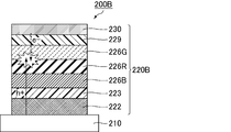
- FIG. 8 is a schematic cross-sectional view showing an example of an organic EL panel having a structure in which conventional light emitting layers of a plurality of colors are laminated.
- the organic EL element 220B provided on the substrate 210 includes, in order from the substrate 210 side, the anode 222, the hole injection layer 223, the blue light emitting layer 226B, the red light emitting layer 226R, and the green color.
- the light emitting layer 226G, the electron injection layer 229, and the cathode 230 are stacked.
- a hole transport layer may be provided between the hole injection layer 223 and the blue light-emitting layer 226B, and an electron transport layer may be provided between the green light-emitting layer 226G and the electron injection layer 229.
- the organic EL element 220B shown in FIG. 8 by controlling the light emitting position, the light emitting materials of the respective colors are efficiently emitted in all three layers of the blue light emitting layer 226B, the red light emitting layer 226R, and the green light emitting layer 226G. This is difficult and has a problem of low luminous efficiency.
- This invention is made
- a mixed light-emitting layer containing both a light-emitting host material and a light-emitting dopant material By providing a light-emitting unit consisting of only a dopant material and laminated with a light-emitting dopant layer formed thinner than a mixed light-emitting layer, the configuration of the carrier recombination region can be optimized and high luminous efficiency can be obtained. I found out that Thus, the inventors have conceived that the above problems can be solved brilliantly and have reached the present invention.
- one embodiment of the present invention is an organic electroluminescence element that includes an anode, a hole transport layer, a light-emitting unit, an electron transport layer, and a cathode in order, and the light-emitting unit includes a mixed light-emitting layer. And a light emitting dopant layer between at least one of the hole transport layer and the mixed light emitting layer and between the electron transport layer and the mixed light emitting layer, wherein the mixed light emitting layer is a first light emitting layer.
- the organic light-emitting device may contain a host material and a first light-emitting dopant material, and the light-emitting dopant layer is substantially composed of only the second light-emitting dopant material and is thinner than the mixed light-emitting layer.
- Another embodiment of the present invention may be an organic electroluminescence panel having a substrate and the organic electroluminescence element disposed on the substrate.
- mixed light emission is achieved by providing a light emitting dopant layer substantially consisting only of a light emitting dopant material as a thin film in the vicinity of a mixed light emitting layer containing both a light emitting host material and a light emitting dopant material.
- a carrier barrier can be less likely to occur at the interface between the layers.
- the carrier recombination region can be made thinner.
- the light emitting dopant layer can be formed by depositing only the light emitting dopant material by short-time vapor deposition or the like. Therefore, the organic EL device of the present invention has high productivity as compared with a conventional configuration in which a plurality of mixed light emitting layers are stacked.
- the organic EL panel of the present invention includes an organic EL element that achieves both high luminous efficiency and high productivity, it achieves excellent productivity, low power consumption and high luminance display devices, lighting devices, and the like. It can be done.
- FIG. 1 is a schematic cross-sectional view showing an organic EL panel of Example 1.
- FIG. 6 is a schematic cross-sectional view showing an organic EL panel of Example 2.
- FIG. 6 is a schematic cross-sectional view showing an organic EL panel of Example 3.
- FIG. 6 is a schematic cross-sectional view showing an organic EL panel of Example 4.
- FIG. 6 is a schematic cross-sectional view showing an organic EL panel of Example 5.
- FIG. 10 is a schematic cross-sectional view showing an organic EL panel of Example 6.
- FIG. It is a cross-sectional schematic diagram which shows an example of the organic EL panel which has the conventional tandem structure.
- organic electroluminescence is also referred to as “organic EL”.
- organic EL organic electroluminescence
- the organic EL element is generally also called an organic light emitting diode (OLED: Organic Light Emitting Diode).
- the organic EL panel of Example 1 includes an organic EL element having an anode, a hole injection layer, a hole transport layer, a light emitting unit, an electron transport layer, an electron injection layer, and a cathode in this order from the substrate side.
- the light emitting unit includes a mixed light emitting layer and light emitting dopant layers disposed on both sides of the mixed light emitting layer.
- the light-emitting dopant layer on the hole transport layer side is described as “first light-emitting dopant layer”
- the light-emitting dopant layer on the electron transport layer side is described as “second light-emitting dopant layer”, and both When referring, it is simply described as “light emitting dopant layer”.
- the light emitting unit has a structure in which the first light emitting dopant layer, the mixed light emitting layer, and the second light emitting dopant layer are stacked in this order from the hole transport side.
- the organic EL element 120A provided on the substrate 110 includes, in order from the substrate 110 side, a reflective electrode 121, an anode 122, a hole injection layer 123, a hole transport layer 124,
- the first light-emitting dopant layer 125, the mixed light-emitting layer 126A, the second light-emitting dopant layer 127, the electron transport layer 128, the electron injection layer 129, and the cathode 130A are stacked.
- the first light emitting dopant layer 125, the mixed light emitting layer 126A, and the second light emitting dopant layer 127 constitute a light emitting unit 140A.
- the substrate 110 a glass substrate, a plastic substrate, or the like can be used.
- a bendable plastic substrate is used as the substrate 110, a flexible organic EL panel can be obtained.
- the substrate 110 is provided with a thin film transistor. The drive of the organic EL element 120A is controlled by electrically connecting the thin film transistor to the reflective electrode 121.
- the reflective electrode 121 disposed below the anode 122 has light reflectivity
- the transparent cathode 130A has light transmittance. That is, the organic EL element 120A of this example is a top emission type element that emits light from the cathode 130A side.
- the arrows in FIG. 1 indicate the traveling direction of light emitted from the organic EL element 120A.
- Silver (Ag) was used as the material of the reflective electrode 121.
- an electrode having light reflectivity can be used.
- an aluminum (Al) layer or an indium (In) layer may be used instead of the above-described one.
- the thickness of the reflective electrode 121 was 100 nm.
- ITO Indium Tin Oxide
- hole injection layer 123 dipyrazino [2,3-f: 2 ′, 3′-h] quinoxaline-2,3,6,7,10,11-hexacarbonitrile (HAT-CN) was used.
- material of the hole injection layer 123 the same hole injection material as that used in a normal organic EL element can be used.
- the thickness of the hole injection layer 123 was 10 nm.
- the hole transport layer 124 As a material for the hole transport layer 124, 4,4′-bis [N- (1-naphthyl) -N-phenyl-amino] -biphenyl ( ⁇ -NPD) was used.
- the hole mobility ⁇ h of ⁇ -NPD is 10 ⁇ 3 to 10 ⁇ 4 cm 2 / Vsec, and the LUMO is about ⁇ 2.4 eV.
- the material of the hole transport layer 124 the same hole transport material as that used in a normal organic EL element can be used, but all contained in the first light emitting dopant layer 125 and the mixed light emitting layer 126A.
- a material having a lowest unoccupied molecular orbital (LUMO) level of 0.1 eV or more is preferably used as compared with the above materials.
- the thickness of the hole transport layer 124 was 20 nm.
- the first light emitting dopant layer 125 is substantially made of only the light emitting dopant material (second light emitting dopant material). That is, the concentration of the second light-emitting dopant material in the first light-emitting dopant layer 125 is 100% by weight or substantially 100% by weight.
- the concentration of the light-emitting dopant material in the light-emitting dopant layer being substantially 100% by weight means that no material that affects the characteristics of the light-emitting dopant layer is contained other than the light-emitting dopant material.
- a small amount of impurities other than the above may be contained, but it is preferable not to contain 3% by weight or more of the light emitting host material.
- the second light-emitting dopant material in the first light-emitting dopant layer 125 either a fluorescent dopant material or a phosphorescent dopant material can be used.
- a fluorescent dopant material or a phosphorescent dopant material
- the second light-emitting dopant material in the first light-emitting dopant layer 125 may be one type or two or more types, but is preferably one type.
- the first light-emitting dopant layer 125 is thinner than the mixed light-emitting layer 126A and is formed in an island shape. That is, there is a portion where the hole transport layer 124 and the mixed light emitting layer 126A are in direct contact.
- the light emitting dopant layer can be formed in an island shape only by shortening the deposition time. Specifically, when an extremely thin film having a maximum film thickness of 1 nm or less is formed by vapor deposition, the formed film becomes an island shape.
- the thickness (maximum film thickness) of the thickest portion of the first light-emitting dopant layer 125 was 0.2 nm.
- a preferable lower limit of the maximum film thickness of the first light-emitting dopant layer 125 is 0.1 nm, a preferable upper limit is 1 nm, and a more preferable upper limit is 0.5 nm.
- the first light emitting dopant layer 125 can be formed by depositing a second light emitting dopant material.
- the concentration of the second light-emitting dopant material is set to 100% by weight or substantially 100% by weight and is formed into an island shape. It is possible to prevent the decrease, (2) the carrier transport is inhibited, the drive voltage is increased, and the light emission efficiency is decreased.
- the mixed light emitting layer 126A is a layer containing at least one kind of light emitting host material (first light emitting host material) and at least one kind of light emitting dopant material (first light emitting dopant material).
- first light emitting host material phosphorescent material type 4,4′-N, N′-dicarbazole-biphenyl (CBP) having a high hole transport property
- CBP N′-dicarbazole-biphenyl
- Ir (pic) 3 is used as the first light-emitting host material.
- the mixture layer contained as one luminescent dopant material was used.
- the hole mobility ⁇ h of CBP is 10 ⁇ 3 to 10 ⁇ 6 cm 2 / Vsec
- the electron mobility ⁇ e is 10 ⁇ 8 to 10 ⁇ 10 cm 2 / Vsec
- the LUMO is about ⁇ 2.6 eV.
- the HOMO is about -5.3 eV.
- the weight ratio of CBP to Ir (pic) 3 was 0.9: 0.1.
- the mixed light emitting layer 126A has a bipolar characteristic in which the electron transporting property and the hole transporting property are similar, and the relationship between the hole mobility ⁇ h and the electron mobility ⁇ e of the first light emitting host material is 0.01 ⁇ e. / ⁇ h ⁇ 100 is preferable, and 0.1 ⁇ e / ⁇ h ⁇ 10 is more preferable.
- the first light-emitting host material is composed of a plurality of types of light-emitting host materials
- the maximum hole mobility ⁇ h is obtained from the individual hole mobility ⁇ h and electron mobility ⁇ e of each light-emitting host material.
- the above relational expression is preferably satisfied when the maximum electron mobility ⁇ e is selected and compared.
- the hole mobility ⁇ h and the electron mobility ⁇ e can be determined by, for example, the time-of-flight method.
- the photoexcited carrier mobility measuring device (trade name: TOF-401, manufactured by Sumitomo Heavy Industries, Ltd.) It can be measured using a measuring device such as.
- the first light-emitting host material a mixture of an electron transporting material and a hole transporting material may be used.
- the first light-emitting dopant material either a fluorescent dopant material or a phosphorescent dopant material can be used.
- the thickness of the mixed light emitting layer 126A was 5 nm.
- the preferable lower limit of the film thickness of the mixed light emitting layer 126A is 2 nm, the preferable upper limit is 10 nm, and the more preferable upper limit is 5 nm.
- the mixed light emitting layer 126A can be formed by co-evaporating the first light emitting host material and the first light emitting dopant material.
- the second light emitting dopant layer 127 is substantially made of only the light emitting dopant material (second light emitting dopant material). That is, the concentration of the second light-emitting dopant material in the second light-emitting dopant layer 127 is 100% by weight or substantially 100% by weight.
- the second light-emitting dopant material in the second light-emitting dopant layer 127 either a fluorescent dopant material or a phosphorescent dopant material can be used.
- a fluorescent dopant material or a phosphorescent dopant material can be used.
- FIrpic [bis (3,5-difluoro-2- (2-pyridylphenyl- (2-carboxypyridyl) iridium (III)]
- the two light emitting dopant materials may be one kind or two kinds or more, but preferably one kind, and the second light emitting dopant material in the second light emitting dopant layer 127 is
- the second light emitting dopant material in the first light emitting dopant layer 125 may include the same kind of the second light emitting dopant material, but the second light emitting dopant material and the second light emitting dopant material in the first light emitting dopant layer 125 may be included.
- the second light emitting dopant material in layer 127 is preferably of a different type.
- the second light-emitting dopant layer 127 is thinner than the mixed light-emitting layer 126A and is formed in an island shape. That is, there is a portion where the electron transport layer 128 and the mixed light emitting layer 126A are in direct contact.
- the thickness (maximum film thickness) of the thickest portion of the second light emitting dopant layer 127 was 0.2 nm.
- a preferable lower limit of the maximum film thickness of the second light-emitting dopant layer 127 is 0.1 nm, a preferable upper limit is 1 nm, and a more preferable upper limit is 0.5 nm.
- the second light emitting dopant layer 127 can be formed by depositing a second light emitting dopant material.
- the first light-emitting dopant material in the mixed light-emitting layer 126A, the first light-emitting dopant layer 125, and the second light-emitting dopant material in the second light-emitting dopant layer 127 have different colors of the three primary colors. It is preferably selected so that it can emit light, and any combination can be used.
- buthophenanthroline (Bphen) was used as a material for the electron transport layer 128, buthophenanthroline (Bphen) was used.
- the same electron transport material as that used in a normal organic EL element can be used, but all materials contained in the mixed light emitting layer 126A and the second light emitting dopant layer 127 are used.
- those having a highest occupied molecular orbital (HOMO) level of 0.1 eV or more are preferably used.
- the electron mobility ⁇ e of Bphen is 10 ⁇ 4 to 10 ⁇ 5 cm 2 / Vsec, and the HOMO is about ⁇ 6.3 eV.
- the thickness of the electron transport layer 128 was 30 nm.
- the electron injection layer 129 As a material for the electron injection layer 129, lithium fluoride (LiF) was used. As a material of the electron injection layer 129, the same electron injection material as that used in a normal organic EL element can be used. The thickness of the electron injection layer 129 was 1 nm.
- the cathode 130A a layer containing Ag and magnesium (Mg) was used.
- the content ratio of Ag and Mg was 0.9: 0.1 on a weight basis.
- the material of the cathode 130A a material having optical transparency and conductivity can be used.
- ITO or indium zinc oxide (IZO) may be used instead of the above materials.
- the thickness of the cathode 130A was 20 nm.
- the light emitting unit 140A has the following characteristics.
- the light-emitting dopant layer 126A is formed by co-evaporation of a light-emitting host material and a light-emitting dopant material, and only one layer is formed. Instead of stacking a plurality of mixed light-emitting layers, a light-emitting dopant layer consisting essentially of a light-emitting dopant material (First light-emitting dopant layer 125 and second light-emitting dopant layer 127) are provided.
- the mixed light emitting layer 126A is a thin film and has bipolar characteristics.
- the first light-emitting dopant layer 125 and the second light-emitting dopant layer 127 are island-shaped ultrathin films. -The LUMO level of the hole transport layer 124 is high and the HOMO level of the electron transport layer 128 is low, and the light emitting unit 140A is blocked without escaping carriers, thereby improving the light emission efficiency.
- the light emitting unit 140A of the present embodiment has the above characteristics, there is no barrier at the interface between the layers containing the light emitting host material, as compared with the conventional light emitting unit in which three mixed light emitting layers are stacked. Carrier barriers hardly occur at the interface between layers. In addition, the thickness of the light emitting unit 140A is reduced. For the above reasons, carriers easily spread over the entire three layers of the first light-emitting dopant layer 125, the mixed light-emitting layer 126A, and the second light-emitting dopant layer 127, and the entire three layers are used as a carrier recombination region. Can do.
- Example 1 relates to a top emission type organic EL panel, but the configuration of the present invention can also be applied to a bottom emission type organic EL panel.
- Example 2 relates to a bottom emission type organic EL panel, and has the same configuration as the organic EL panel of Example 1 except for the configuration of a pair of electrodes.
- FIG. 2 is a schematic cross-sectional view showing the organic EL panel of Example 2.
- the organic EL element 120B provided on the substrate 110 includes an anode 122, a hole injection layer 123, a hole transport layer 124, and a first light emission in order from the substrate 110 side.
- the dopant layer 125, the mixed light emitting layer 126A, the second light emitting dopant layer 127, the electron transport layer 128, the electron injection layer 129, and the cathode 130B are stacked.
- the arrows in FIG. 2 indicate the traveling direction of light emitted from the organic EL element 120B.
- ITO is used as the material of the anode 122.
- the thickness of the anode 122 was 100 nm.
- the cathode 130B aluminum (Al) was used as the material of the cathode 130B.
- the thickness of the cathode 130B was 100 nm.
- the carrier recombination region extends over the entire three layers of the first light-emitting dopant layer 125, the mixed light-emitting layer 126A, and the second light-emitting dopant layer 127.
- a device capable of white display that can efficiently emit light of all three kinds of light-emitting dopant materials included can be realized.
- Example 3 In Example 1, CBP having a high hole transporting property was used as the first light emitting host material in the mixed light emitting layer 126A. However, in the present invention, the mixed light emitting layer may contain two or more kinds of light emitting host materials. Good. In Example 3, CBP having a high hole transporting property and 2,2 ′, 2 ′′-(1,3,5-Benzinetriyl) -tris (1-phenyl) having a high electron transporting property are used as the first light-emitting host material. The structure is the same as that of the organic EL panel of Example 1, except that a mixture of -1-H-benzimidazole (TPBI) at a weight ratio of 1: 1 is used.
- TPBI -1-H-benzimidazole
- FIG. 3 is a schematic cross-sectional view showing the organic EL panel of Example 3.
- the organic EL element 120C provided on the substrate 110 includes, in order from the substrate 110 side, a reflective electrode 121, an anode 122, a hole injection layer 123, a hole transport layer 124, The first light emitting dopant layer 125, the mixed light emitting layer 126B, the second light emitting dopant layer 127, the electron transport layer 128, the electron injection layer 129, and the cathode 130A are stacked.
- the first light emitting dopant layer 125, the mixed light emitting layer 126B, and the second light emitting dopant layer 127 constitute the light emitting unit 140B.
- the arrows in FIG. 3 indicate the traveling direction of light emitted from the organic EL element 120C.
- the mixed light emitting layer 126B contains CBP having a high hole transporting property and TPBI having a high electron transporting property as the first light emitting host material, and Ir (pic) 3 as the first light emitting dopant material.
- a mixture layer was used.
- the electron mobility ⁇ e of TPBI is about 10 ⁇ 5 to 10 ⁇ 6 cm 2 / Vsec, LUMO is about ⁇ 2.8 eV, and HOMO is about ⁇ 5.7 eV.
- the weight ratio of CBP, TPBI, and Ir (pic) 3 was 0.45: 0.45: 0.1.
- the thickness of the mixed light emitting layer 126B was 5 nm.
- the carrier recombination region extends over the entire three layers of the first light-emitting dopant layer 125, the mixed light-emitting layer 126B, and the second light-emitting dopant layer 127.
- a device capable of white display that can efficiently emit light of all three kinds of light-emitting dopant materials included can be realized.
- the bipolar property of the mixed light emitting layer 126B is higher than that of the mixed light emitting layer 126A, further improvement in efficiency can be realized.
- Example 4 In Example 1, the first light-emitting dopant layer 125 and the second light-emitting dopant layer 127 are disposed on both sides of the mixed light-emitting layer 126A. However, in the present invention, the light-emitting dopant layer is disposed only on one side of the mixed light-emitting layer. May be. In Example 4, instead of the light emitting unit 140A configured by the first light emitting dopant layer 125, the mixed light emitting layer 126A, and the second light emitting dopant layer 127, the first light emitting dopant layer is not included, and the mixed light emitting layer is used.
- the organic EL panel has the same configuration as that of the organic EL panel of Example 1 except that a light emitting unit in which the material is changed is used.
- FIG. 4 is a schematic cross-sectional view showing the organic EL panel of Example 4.
- the organic EL element 120D provided on the substrate 110 includes, in order from the substrate 110 side, a reflective electrode 121, an anode 122, a hole injection layer 123, a hole transport layer 124,
- the mixed light emitting layer 126C, the second light emitting dopant layer 127, the electron transport layer 128, the electron injection layer 129, and the cathode 130A are stacked.
- the mixed light emitting layer 126C and the second light emitting dopant layer 127 constitute a light emitting unit 140C.
- the arrows in FIG. 4 indicate the traveling direction of light emitted from the organic EL element 120D.
- the mixed light-emitting layer 126C a mixture layer containing CBP having a high hole transporting property as the first light-emitting host material and Ir (bzq) 3 as the first light-emitting dopant material was used.
- the weight ratio of CBP and Ir (bzq) 3 was 0.9: 0.1.
- the thickness of the mixed light emitting layer 126C was 5 nm.
- the first light-emitting dopant layer 125 is not provided, but the second light-emitting dopant layer 127 that emits blue light by using a material that emits yellow, which is an intermediate color, for the mixed light-emitting layer 126C.
- a device capable of white display can be realized.
- the structure can be simplified by omitting the first light-emitting dopant layer 125, there is a possibility that the color reproducibility of a single color is not sufficient in a display application, which is particularly suitable for an illumination application.
- the carrier recombination region extends over the entire two layers of the mixed light-emitting layer 126C and the second light-emitting dopant layer 127, and all of the two types of light-emitting dopant materials contained in the two layers can emit light efficiently.
- Example 5 is the same as the organic EL panel of Example 1 except that a block layer containing the first light-emitting host material is inserted between the mixed light-emitting layer 126A and the second light-emitting dopant layer 127. It has a configuration.
- FIG. 5 is a schematic cross-sectional view showing an organic EL panel of Example 5.
- the organic EL element 120E provided on the substrate 110 includes, in order from the substrate 110 side, the reflective electrode 121, the anode 122, the hole injection layer 123, the hole transport layer 124, The first light emitting dopant layer 125, the mixed light emitting layer 126A, the block layer 131, the second light emitting dopant layer 127, the electron transport layer 128, the electron injection layer 129, and the cathode 130A are stacked.
- the first light emitting dopant layer 125, the mixed light emitting layer 126A, the block layer 131, and the second light emitting dopant layer 127 constitute a light emitting unit 140D.
- the arrows in FIG. 5 indicate the traveling direction of the light emitted from the organic EL element 120E.
- the block layer 131 is inserted between the mixed light emitting layer 126A and the second light emitting dopant layer 127, so that the first light emitting dopant material in the mixed light emitting layer 126A and the second light emitting material are emitted.
- the second light-emitting dopant material in the dopant layer 127 is prevented from contacting, thereby preventing deactivation due to interaction between excitons and further improving the light emission efficiency.
- the material of the block layer 131 is not particularly limited as long as it can transport both electron and hole carriers.
- a hole transport material such as TPD and TCTA, and an electron transport material such as Alq 3 and BCP are used.
- a light-emitting host material is preferably used because it easily excites the dopant material.
- the first light emitting host material included in the mixed light emitting layer 126A may be used, or the light emitting host material (second light emitting host) not included in the mixed light emitting layer 126A. Material) may be used, or the first light emitting host material and the second light emitting host material may be used in combination.
- CBP corresponding to the first light emitting host material was used as the material of the block layer 131.
- the material of the block layer 131 preferably satisfies 0.01 ⁇ e / ⁇ h ⁇ 100 and more preferably satisfies 0.1 ⁇ e / ⁇ h ⁇ 10 in the relationship between the hole mobility ⁇ h and the electron mobility ⁇ e. preferable.
- the block layer 131 contains both the first light-emitting host material and the second light-emitting host material, the individual hole mobility ⁇ h and electron mobility ⁇ e of the first and second light-emitting host materials. Therefore, it is preferable that the above relational expression is satisfied when the maximum hole mobility ⁇ h and the maximum electron mobility ⁇ e are selected and compared.
- the second light emitting host material has a relationship between the hole mobility ⁇ h and the electron mobility ⁇ e of 0.01 ⁇ e / A material satisfying ⁇ h ⁇ 100 is preferable, and a material satisfying 0.1 ⁇ e / ⁇ h ⁇ 10 is more preferable.
- the thickness of the block layer 131 was 5 nm.
- the material of the electron transport layer 128 is HOMO as compared with all materials contained in the mixed light emitting layer 126A and the second light emitting dopant layer 127 and all materials contained in the block layer 131.
- a material whose level is lower by 0.1 eV or more is preferably used.
- the carrier recombination region extends over the entire three layers of the first light-emitting dopant layer 125, the mixed light-emitting layer 126B, and the second light-emitting dopant layer 127.
- a device capable of white display that can efficiently emit light of all three kinds of light-emitting dopant materials included can be realized.
- the block layer 131 is provided only on the electron transport layer 128 side with respect to the mixed light emitting layer 126A, but may be provided only on the hole transport layer 124 side with respect to the mixed light emitting layer 126A. Alternatively, it may be provided on both sides of the electron transport layer 128 side and the hole transport layer 124 side with respect to the mixed light emitting layer 126A.
- the material of the hole transport layer 124 includes all materials contained in the first light-emitting dopant layer 125 and the mixed light-emitting layer 126A, and the block layer.
- a material having a LUMO level higher by 0.1 eV or more than all materials contained in 131 is preferably used.
- Example 6 In the sixth embodiment, the principle of white display will be described.
- Example 6 has the same configuration as that of the organic EL panel of Example 1 except that the configuration of the anode is changed.
- FIG. 6 is a schematic cross-sectional view showing the organic EL panel of Example 6.
- the organic EL element 120F provided on the substrate 110 includes, in order from the substrate 110 side, the reflective electrode 121, the anode 122, the hole injection layer 123, the hole transport layer 124, The first light-emitting dopant layer 125, the mixed light-emitting layer 126A, the second light-emitting dopant layer 127, the electron transport layer 128, the electron injection layer 129, and the cathode 130A are stacked.
- each pixel includes a blue pixel anode 122B, a green pixel anode 122G, and a red pixel anode 122R.
- the arrows in FIG. 6 indicate the traveling directions of the three primary colors of RGB emitted from the organic EL element 120F.
- the blue pixel anode 122B is made of a 20 nm thick ITO film
- the green pixel anode 122G is made of a 60 nm thick ITO film
- the red pixel anode 122R is made of a 100 nm thick ITO film.
- the organic EL panel of Example 6 since the thickness of the anode 122 is different for each pixel, different optical interference occurs for each pixel, and light of different colors can be extracted. Since various colors are displayed by combining the three primary colors of RGB in the display application, the configuration of the sixth embodiment is suitable for the display application. Further, providing a difference in the thickness of the anode 122 for each pixel can be realized without a high-definition deposition mask.
- the light emitting dopant layer may have a thickness of 1 nm or less. As a result, the light emitting dopant layer can be formed in an island shape, and carriers can be expanded throughout the light emitting unit to emit light efficiently.
- the relationship between the hole mobility ⁇ h and the electron mobility ⁇ e of the first light emitting host material may satisfy 0.01 ⁇ e / ⁇ h ⁇ 100. As described above, by increasing the bipolar property of the light-emitting host material, higher efficiency can be realized.
- the light emitting dopant layer includes a first light emitting dopant layer positioned between the hole transport layer and the mixed light emitting layer, and the material constituting the hole transport layer includes the mixed light emitting layer and the first light emitting layer.
- the energy level of the lowest vacant orbit may be higher by 0.1 eV or more.
- the light emitting dopant layer includes a second light emitting dopant layer positioned between the electron transport layer and the mixed light emitting layer, and the material constituting the electron transport layer includes the mixed light emitting layer and the second light emitting layer.
- the energy level of the highest occupied orbital may be lower by 0.1 eV or more.
- the light emitting unit may include a block layer between the mixed light emitting layer and the light emitting dopant layer, and the block layer may contain a material capable of transporting both electron and hole carriers.
- the relationship between the hole mobility ⁇ h and the electron mobility ⁇ e of the block layer material may satisfy 0.01 ⁇ e / ⁇ h ⁇ 100. As described above, by increasing the bipolar property of the second light-emitting host material, it is possible to further increase the efficiency.
- the light-emitting unit includes, from the hole transport layer side, a first light-emitting dopant layer as the light-emitting dopant layer, a first block layer as the block layer, and the mixed light-emitting layer, and the hole transport
- the material constituting the layer has an energy level of the lowest vacant orbit of 0.1 eV or more as compared with all materials contained in the mixed light emitting layer, the first block layer, and the first light emitting dopant layer. It may be expensive. Thereby, electrons (carriers) injected from the electron transport layer side into the mixed light emitting layer are suppressed from flowing into the hole transport layer side, and a decrease in light emission efficiency can be prevented.
- the light emitting unit includes, from the electron transport layer side, a second light emitting dopant layer as the light emitting dopant layer, a second block layer as the block layer, and the mixed light emitting layer.
- the constituent material is higher in energy level of the highest occupied orbital by 0.1 eV or more than all materials contained in the mixed light emitting layer, the second block layer, and the second light emitting dopant layer. It may be a thing. As a result, holes (carriers) injected from the hole transport layer side into the mixed light emitting layer are suppressed from flowing into the electron transport layer side, and a reduction in light emission efficiency can be prevented.
Landscapes
- Physics & Mathematics (AREA)
- Optics & Photonics (AREA)
- Electromagnetism (AREA)
- Electroluminescent Light Sources (AREA)
Abstract
Description
実施例1の有機ELパネルは、基板側から順に、陽極、正孔注入層、正孔輸送層、発光ユニット、電子輸送層、電子注入層及び陰極を有する有機EL素子を備えるものである。発光ユニットは、混合発光層と、混合発光層の両側にそれぞれ配置された発光ドーパント層とを含む。本明細書では、正孔輸送層側の発光ドーパント層を「第一の発光ドーパント層」と記載し、電子輸送層側の発光ドーパント層を「第二の発光ドーパント層」と記載し、両方を指す場合は単に「発光ドーパント層」と記載する。以上のように、発光ユニットは、正孔輸送側から順に、第一の発光ドーパント層、混合発光層、第二の発光ドーパント層が積層された構造を有するものである。
・発光ホスト材料と発光ドーパント材料とを共蒸着して形成される混合発光層126Aは1層だけとし、複数の混合発光層を積層する代わりに、実質的に発光ドーパント材料のみからなる発光ドーパント層(第一の発光ドーパント層125及び第二の発光ドーパント層127)を設けている。
・混合発光層126Aは、薄膜であり、かつバイポーラ特性である。
・第一の発光ドーパント層125及び第二の発光ドーパント層127は、島状の極薄膜である。
・正孔輸送層124のLUMO準位が高く、電子輸送層128のHOMO準位が低く、発光ユニット140Aからキャリアを逃がさずにブロックし、発光効率を向上させている。
実施例1は、トップ・エミッション型の有機ELパネルに関するものであったが、ボトム・エミッション型の有機ELパネルに、本発明の構成を適用することも可能である。実施例2は、ボトム・エミッション型の有機ELパネルに関し、一対の電極の構成以外は、実施例1の有機ELパネルと同様の構成を有する。
実施例1では、混合発光層126A中の第一の発光ホスト材料として、正孔輸送性が高いCBPを用いたが、本発明において、混合発光層は、2種類以上の発光ホスト材料を含んでもよい。実施例3は、第一の発光ホスト材料として、正孔輸送性が高いCBPと、電子輸送性が高い2,2’,2” -(1,3,5-Benzinetriyl)-tris(1-phenyl-1-H-benzimidazole(TPBI)とを1:1の重量比で混合させたものを用いたこと以外は、実施例1の有機ELパネルと同様の構成を有する。
実施例1では、混合発光層126Aの両側に、第一の発光ドーパント層125及び第二の発光ドーパント層127を配置したが、本発明において、発光ドーパント層は、混合発光層の片側のみに配置してもよい。実施例4は、第一の発光ドーパント層125、混合発光層126A及び第二の発光ドーパント層127によって構成される発光ユニット140Aの代わりに、第一の発光ドーパント層を含まず、かつ混合発光層の材料が変更された発光ユニットを用いたこと以外は、実施例1の有機ELパネルと同様の構成を有する。
実施例5は、混合発光層126Aと第二の発光ドーパント層127との間に、第一の発光ホスト材料を含有するブロック層を挿入したこと以外は、実施例1の有機ELパネルと同様の構成を有する。
実施例6では、白色表示の原理を説明する。実施例6は、陽極の構成を変更したこと以外は、実施例1の有機ELパネルと同様の構成を有する。
以下に、本発明に係る有機EL素子の好ましい態様の例を挙げる。各例は、本発明の要旨を逸脱しない範囲において適宜組み合わされてもよい。
110、210:基板
120A、120B、120C、120D、120E、120F、220A、220B:有機EL素子
121:反射電極
122、222:陽極
122B:青の画素の陽極
122G:緑の画素の陽極
122R:赤の画素の陽極
123、223:正孔注入層
124:正孔輸送層
125:第一の発光ドーパント層
126A、126B、126C:混合発光層
127:第二の発光ドーパント層
128:電子輸送層
129、229:電子注入層
130A、130B、230:陰極
131:ブロック層
140A、140B、140C、140D:発光ユニット
226B:青色発光層
226G:緑色発光層
226R:赤色発光層
226Y:黄色発光層
231:中間層
Claims (10)
- 陽極と、
正孔輸送層と、
発光ユニットと、
電子輸送層と、
陰極とを順に有する有機エレクトロルミネッセンス素子であって、
前記発光ユニットは、混合発光層を含み、かつ前記正孔輸送層と前記混合発光層との間、及び、前記電子輸送層と前記混合発光層との間の少なくとも一方に発光ドーパント層を含み、
前記混合発光層は、第一の発光ホスト材料及び第一の発光ドーパント材料を含有し、
前記発光ドーパント層は、実質的に第二の発光ドーパント材料のみからなり、前記混合発光層よりも薄いことを特徴とする有機エレクトロルミネッセンス素子。 - 前記発光ドーパント層の厚みは、1nm以下であることを特徴とする請求項1記載の有機エレクトロルミネッセンス素子。
- 前記第一の発光ホスト材料の正孔移動度μhと電子移動度μeの関係が、0.01<μe/μh<100を満たすことを特徴とする請求項1又は2に記載の有機エレクトロルミネッセンス素子。
- 前記発光ドーパント層は、前記正孔輸送層と前記混合発光層との間に位置する第一の発光ドーパント層を含み、
前記正孔輸送層を構成する材料は、前記混合発光層及び前記第一の発光ドーパント層中に含有される全ての材料と比べて、最低空軌道のエネルギー準位が0.1eV以上高いことを特徴とする請求項1~3のいずれかに記載の有機エレクトロルミネッセンス素子。 - 前記発光ドーパント層は、前記電子輸送層と前記混合発光層との間に位置する第二の発光ドーパント層を含み、
前記電子輸送層を構成する材料は、前記混合発光層及び前記第二の発光ドーパント層中に含有される全ての材料と比べて、最高被占軌道のエネルギー準位が0.1eV以上低いことを特徴とする請求項1~3のいずれかに記載の有機エレクトロルミネッセンス素子。 - 前記発光ユニットは、前記混合発光層と前記発光ドーパント層との間にブロック層を含み、
前記ブロック層は、電子及び正孔の両キャリアを輸送できる材料を含有することを特徴とする請求項1~5のいずれかに記載の有機エレクトロルミネッセンス素子。 - 前記ブロック層の材料の正孔移動度μhと電子移動度μeの関係が、0.01<μe/μh<100を満たすことを特徴とする請求項6に記載の有機エレクトロルミネッセンス素子。
- 前記発光ユニットは、前記正孔輸送層側から、前記発光ドーパント層としての第一の発光ドーパント層、前記ブロック層としての第一のブロック層、及び、前記混合発光層を含み、
前記正孔輸送層を構成する材料は、前記混合発光層、前記第一のブロック層及び前記第一の発光ドーパント層中に含有される全ての材料と比べて、最低空軌道のエネルギー準位が0.1eV以上高いことを特徴とする請求項6又は7に記載の有機エレクトロルミネッセンス素子。 - 前記発光ユニットは、前記電子輸送層側から、前記発光ドーパント層としての第二の発光ドーパント層、前記ブロック層としての第二のブロック層、及び、前記混合発光層を含み、
前記電子輸送層を構成する材料は、前記混合発光層、前記第二のブロック層及び前記第二の発光ドーパント層中に含有される全ての材料と比べて、最高被占軌道のエネルギー準位が0.1eV以上低いことを特徴とする請求項6~8のいずれかに記載の有機エレクトロルミネッセンス素子。 - 基板と、前記基板上に配置された請求項1~9のいずれかに記載の有機エレクトロルミネッセンス素子とを有することを特徴とする有機エレクトロルミネッセンスパネル。
Priority Applications (3)
| Application Number | Priority Date | Filing Date | Title |
|---|---|---|---|
| CN201580006196.8A CN105981476B (zh) | 2014-02-18 | 2015-02-10 | 有机电致发光元件和有机电致发光面板 |
| US15/117,771 US9966550B2 (en) | 2014-02-18 | 2015-02-10 | Organic electroluminescent element and organic electroluminescent panel |
| JP2016504047A JP6294460B2 (ja) | 2014-02-18 | 2015-02-10 | 有機エレクトロルミネッセンス素子、及び、有機エレクトロルミネッセンスパネル |
Applications Claiming Priority (2)
| Application Number | Priority Date | Filing Date | Title |
|---|---|---|---|
| JP2014-028778 | 2014-02-18 | ||
| JP2014028778 | 2014-02-18 |
Publications (1)
| Publication Number | Publication Date |
|---|---|
| WO2015125653A1 true WO2015125653A1 (ja) | 2015-08-27 |
Family
ID=53878158
Family Applications (1)
| Application Number | Title | Priority Date | Filing Date |
|---|---|---|---|
| PCT/JP2015/053574 Ceased WO2015125653A1 (ja) | 2014-02-18 | 2015-02-10 | 有機エレクトロルミネッセンス素子、及び、有機エレクトロルミネッセンスパネル |
Country Status (5)
| Country | Link |
|---|---|
| US (1) | US9966550B2 (ja) |
| JP (1) | JP6294460B2 (ja) |
| CN (1) | CN105981476B (ja) |
| TW (1) | TWI584462B (ja) |
| WO (1) | WO2015125653A1 (ja) |
Cited By (1)
| Publication number | Priority date | Publication date | Assignee | Title |
|---|---|---|---|---|
| KR102039452B1 (ko) * | 2018-05-15 | 2019-11-04 | (주)에이프로 | 에너지 장벽을 이용한 다중 도핑 고연색 단일 발광층의 백색 유기 발광 다이오드 |
Families Citing this family (11)
| Publication number | Priority date | Publication date | Assignee | Title |
|---|---|---|---|---|
| CN104835919A (zh) * | 2015-05-26 | 2015-08-12 | 京东方科技集团股份有限公司 | 一种电致发光器件及其制备方法、显示基板、显示装置 |
| TWI634684B (zh) * | 2017-10-18 | 2018-09-01 | 國立清華大學 | 高效率有機發光二極體元件 |
| US20220209166A1 (en) * | 2019-04-11 | 2022-06-30 | Sharp Kabushiki Kaisha | Light-emitting element and display device |
| KR102500996B1 (ko) * | 2019-07-12 | 2023-02-20 | 삼성디스플레이 주식회사 | 발광 소자 및 이를 포함하는 표시 패널 |
| CN110982347A (zh) * | 2019-12-16 | 2020-04-10 | 深圳市华星光电半导体显示技术有限公司 | 用于喷墨打印有机发光二极管的墨水组合物及其制造方法 |
| US11441045B2 (en) | 2019-12-16 | 2022-09-13 | Shenzhen China Star Optoelectronics Semiconductor Display Technology Co., Ltd. | Ink composition for inkjet printing organic light-emitting diodes and method of manufacturing the same |
| KR20210109720A (ko) | 2020-02-27 | 2021-09-07 | 삼성디스플레이 주식회사 | 유기 발광 소자의 제조 방법 및 이에 의하여 제조된 유기 발광 소자 |
| CN111933812B (zh) * | 2020-08-17 | 2024-01-26 | 云谷(固安)科技有限公司 | 显示面板 |
| US12185557B2 (en) * | 2020-12-04 | 2024-12-31 | The Regents Of The University Of Michigan | Optoelectronic device including ultrathin dopant layers |
| WO2022141621A1 (zh) * | 2021-01-04 | 2022-07-07 | 京东方科技集团股份有限公司 | 有机发光器件、发光基板和发光装置 |
| CN113555508B (zh) * | 2021-07-16 | 2022-10-04 | 京东方科技集团股份有限公司 | 一种荧光发光器件及其制备方法、显示面板、显示装置 |
Citations (6)
| Publication number | Priority date | Publication date | Assignee | Title |
|---|---|---|---|---|
| JP2009048893A (ja) * | 2007-08-21 | 2009-03-05 | Tosoh Corp | 有機el素子 |
| JP2009260308A (ja) * | 2008-03-18 | 2009-11-05 | Semiconductor Energy Lab Co Ltd | 発光素子、発光装置及び電子機器 |
| JP2012124360A (ja) * | 2010-12-09 | 2012-06-28 | Konica Minolta Holdings Inc | 多色燐光発光有機エレクトロルミネッセンス素子及び照明装置 |
| JP2012151322A (ja) * | 2011-01-20 | 2012-08-09 | Konica Minolta Holdings Inc | 白色発光有機エレクトロルミネッセンス素子及び照明装置 |
| JP2013026301A (ja) * | 2011-07-19 | 2013-02-04 | Hitachi Ltd | 有機発光素子、光源装置および有機発光素子の製造方法 |
| JP2013546139A (ja) * | 2010-11-11 | 2013-12-26 | 日東電工株式会社 | ハイブリッドコンポジット発光性構成体およびこれを使用する発光デバイス |
Family Cites Families (13)
| Publication number | Priority date | Publication date | Assignee | Title |
|---|---|---|---|---|
| US7622200B2 (en) * | 2004-05-21 | 2009-11-24 | Semiconductor Energy Laboratory Co., Ltd. | Light emitting element |
| US7273663B2 (en) | 2004-08-20 | 2007-09-25 | Eastman Kodak Company | White OLED having multiple white electroluminescence units |
| US7776456B2 (en) | 2004-12-03 | 2010-08-17 | Universal Display Corporation | Organic light emitting devices with an emissive region having emissive and non-emissive layers and method of making |
| US7772761B2 (en) * | 2005-09-28 | 2010-08-10 | Osram Opto Semiconductors Gmbh | Organic electrophosphorescence device having interfacial layers |
| US7332860B2 (en) | 2006-03-30 | 2008-02-19 | Eastman Kodak Company | Efficient white-light OLED display with filters |
| US8546816B2 (en) * | 2007-04-30 | 2013-10-01 | Novaled Ag | Light-emitting component and method for the production thereof |
| TWI467824B (zh) | 2009-06-11 | 2015-01-01 | Ind Tech Res Inst | 白光有機發光元件 |
| JP5649327B2 (ja) | 2010-04-22 | 2015-01-07 | ユー・ディー・シー アイルランド リミテッド | 有機電界発光素子 |
| US8933436B2 (en) * | 2010-10-13 | 2015-01-13 | The Regents Of The University Of Michigan | Ordered organic-organic multilayer growth |
| WO2014088667A2 (en) * | 2012-09-14 | 2014-06-12 | Qd Vision, Inc. | Light emitting device including tandem structure |
| TW201414031A (zh) * | 2012-09-21 | 2014-04-01 | Nat Univ Tsing Hua | 利用能隙匹配之染料作為共主體之有機發光二極體 |
| TWI556486B (zh) * | 2012-12-20 | 2016-11-01 | 財團法人工業技術研究院 | 白光有機發光二極體 |
| US9978812B2 (en) * | 2014-01-14 | 2018-05-22 | Sharp Kabushiki Kaisha | Organic electroluminescent display panel |
-
2015
- 2015-02-10 WO PCT/JP2015/053574 patent/WO2015125653A1/ja not_active Ceased
- 2015-02-10 JP JP2016504047A patent/JP6294460B2/ja active Active
- 2015-02-10 CN CN201580006196.8A patent/CN105981476B/zh active Active
- 2015-02-10 US US15/117,771 patent/US9966550B2/en active Active
- 2015-02-16 TW TW104105422A patent/TWI584462B/zh not_active IP Right Cessation
Patent Citations (6)
| Publication number | Priority date | Publication date | Assignee | Title |
|---|---|---|---|---|
| JP2009048893A (ja) * | 2007-08-21 | 2009-03-05 | Tosoh Corp | 有機el素子 |
| JP2009260308A (ja) * | 2008-03-18 | 2009-11-05 | Semiconductor Energy Lab Co Ltd | 発光素子、発光装置及び電子機器 |
| JP2013546139A (ja) * | 2010-11-11 | 2013-12-26 | 日東電工株式会社 | ハイブリッドコンポジット発光性構成体およびこれを使用する発光デバイス |
| JP2012124360A (ja) * | 2010-12-09 | 2012-06-28 | Konica Minolta Holdings Inc | 多色燐光発光有機エレクトロルミネッセンス素子及び照明装置 |
| JP2012151322A (ja) * | 2011-01-20 | 2012-08-09 | Konica Minolta Holdings Inc | 白色発光有機エレクトロルミネッセンス素子及び照明装置 |
| JP2013026301A (ja) * | 2011-07-19 | 2013-02-04 | Hitachi Ltd | 有機発光素子、光源装置および有機発光素子の製造方法 |
Cited By (1)
| Publication number | Priority date | Publication date | Assignee | Title |
|---|---|---|---|---|
| KR102039452B1 (ko) * | 2018-05-15 | 2019-11-04 | (주)에이프로 | 에너지 장벽을 이용한 다중 도핑 고연색 단일 발광층의 백색 유기 발광 다이오드 |
Also Published As
| Publication number | Publication date |
|---|---|
| JP6294460B2 (ja) | 2018-03-14 |
| TW201535709A (zh) | 2015-09-16 |
| US9966550B2 (en) | 2018-05-08 |
| CN105981476A (zh) | 2016-09-28 |
| JPWO2015125653A1 (ja) | 2017-03-30 |
| US20160359128A1 (en) | 2016-12-08 |
| TWI584462B (zh) | 2017-05-21 |
| CN105981476B (zh) | 2018-01-12 |
Similar Documents
| Publication | Publication Date | Title |
|---|---|---|
| JP6294460B2 (ja) | 有機エレクトロルミネッセンス素子、及び、有機エレクトロルミネッセンスパネル | |
| US10418580B2 (en) | Organic electroluminescent device and organic electroluminescent display device | |
| JP6246990B2 (ja) | 有機発光ダイオード装置 | |
| US8288784B2 (en) | Organic light emitting display device | |
| KR101094282B1 (ko) | 유기 발광 장치 | |
| KR102089329B1 (ko) | 유기 발광 표시 장치 | |
| US9293736B2 (en) | Organic light emitting element having emission layers and an electron injection layer including fullerene and lithium quinolate | |
| KR102149685B1 (ko) | 유기 발광 소자 | |
| KR20130007873A (ko) | 유기발광소자 | |
| US9130185B2 (en) | Organic light emitting diode | |
| WO2015064432A1 (ja) | 有機エレクトロルミネッセンス素子、及び、有機エレクトロルミネッセンス表示パネル | |
| CN106449720B (zh) | 一种有机发光显示面板和有机发光显示装置 | |
| KR20130057738A (ko) | 유기전계발광소자 | |
| CN106654033A (zh) | 一种有机发光显示面板以及电子设备 | |
| KR101878328B1 (ko) | 유기전계 발광소자 | |
| US11805663B2 (en) | Light emitting device and display device | |
| KR20160037778A (ko) | 유기 발광 소자 | |
| CN106409877A (zh) | 一种有机发光显示面板和有机发光显示装置 | |
| WO2015163265A1 (ja) | 有機エレクトロルミネッセンス素子、及び、有機エレクトロルミネッセンスパネル | |
| KR101845309B1 (ko) | 유기전계 발광소자 | |
| JP2012156075A (ja) | 表示装置 | |
| US10305056B2 (en) | Organic electroluminescent element and organic electroluminescent panel | |
| KR102550746B1 (ko) | 유기 발광 표시 장치 | |
| JP2007180376A (ja) | 有機エレクトロルミネッセント素子及び有機エレクトロルミネッセント表示装置 |
Legal Events
| Date | Code | Title | Description |
|---|---|---|---|
| 121 | Ep: the epo has been informed by wipo that ep was designated in this application |
Ref document number: 15751684 Country of ref document: EP Kind code of ref document: A1 |
|
| ENP | Entry into the national phase |
Ref document number: 2016504047 Country of ref document: JP Kind code of ref document: A |
|
| WWE | Wipo information: entry into national phase |
Ref document number: 15117771 Country of ref document: US |
|
| NENP | Non-entry into the national phase |
Ref country code: DE |
|
| 122 | Ep: pct application non-entry in european phase |
Ref document number: 15751684 Country of ref document: EP Kind code of ref document: A1 |