WO2015125458A1 - 発光装置および発光装置の製造方法 - Google Patents
発光装置および発光装置の製造方法 Download PDFInfo
- Publication number
- WO2015125458A1 WO2015125458A1 PCT/JP2015/000711 JP2015000711W WO2015125458A1 WO 2015125458 A1 WO2015125458 A1 WO 2015125458A1 JP 2015000711 W JP2015000711 W JP 2015000711W WO 2015125458 A1 WO2015125458 A1 WO 2015125458A1
- Authority
- WO
- WIPO (PCT)
- Prior art keywords
- layer
- metal
- emitting device
- light
- metal layer
- Prior art date
- Legal status (The legal status is an assumption and is not a legal conclusion. Google has not performed a legal analysis and makes no representation as to the accuracy of the status listed.)
- Ceased
Links
Images





Classifications
-
- H—ELECTRICITY
- H10—SEMICONDUCTOR DEVICES; ELECTRIC SOLID-STATE DEVICES NOT OTHERWISE PROVIDED FOR
- H10K—ORGANIC ELECTRIC SOLID-STATE DEVICES
- H10K59/00—Integrated devices, or assemblies of multiple devices, comprising at least one organic light-emitting element covered by group H10K50/00
- H10K59/80—Constructional details
- H10K59/805—Electrodes
- H10K59/8051—Anodes
- H10K59/80518—Reflective anodes, e.g. ITO combined with thick metallic layers
Definitions
- the present invention relates to a light emitting device including an EL layer and a method for manufacturing the light emitting device.
- Some light emitting devices have a hole injection layer disposed between an anode and an EL layer to improve luminous efficiency.
- a highly reflective material including an alloy
- an oxide of a transition metal including an alloy
- the hole injection layer is formed by a reactive sputtering method using oxygen plasma using a metal target member containing a transition metal. Specifically, argon gas and oxygen gas are supplied into a vacuum container that houses the target member, and sputtering is performed.
- the surface of the target member is oxidized, and the oxide on the surface is sputtered to form a metal oxide layer on the anode.
- oxygen plasma has a characteristic that it is very easy to oxidize metals. Therefore, when a hole injection layer is formed by a reactive sputtering method, for example, when aluminum or silver is used as the anode, the surface of the anode is oxidized.
- the surface of the anode is oxidized, the surface of the anode is blackened, the light reflection function is lowered, and the light emission luminance of the light emitting device is lowered.
- the anode has a high electrical resistance, the amount of current necessary for light emission does not flow, and the light emission luminance of the light emitting device is lowered. Note that if a larger voltage is applied between the anode and the cathode in order to flow a current necessary for light emission, the life of the light emitting device (EL layer) is shortened.
- Patent Document 1 a technique has been proposed in which a metal layer made of nickel (Ni) is formed on the upper surface of the anode to prevent the anode from being oxidized.
- the nickel layer is formed by an electroless plating method using a plating solution. For this reason, work such as removal of the solution after immersion is necessary, and time and labor are required for forming the nickel layer, and the manufacturing process of the light emitting device becomes complicated.
- the present invention provides a light-emitting device and a method for manufacturing the light-emitting device that can easily form an anti-oxidation metal layer on the surface of the first electrode containing aluminum or silver. Objective.
- a light-emitting device includes a first electrode containing aluminum or silver, a metal layer formed on an upper surface of the first electrode, and an upper surface of the metal layer. And a metal oxide layer made of a metal oxide containing a transition metal, an EL layer formed on the metal oxide layer, and a second electrode formed on the EL layer, The layer contains the same metal as the transition metal.
- the metal layer contains the same metal as the transition metal constituting the metal oxide layer. Therefore, when forming the metal layer, a metal layer other than the metal for the metal oxide layer There is little preparation of a dedicated metal, and a metal layer can be easily provided.
- FIG. 3 is a schematic cross-sectional view showing a configuration in the AA cross section of FIG.
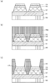
- It is process drawing for demonstrating the formation process of a display panel, Comprising: (a) is process drawing for demonstrating an insulating layer formation process, (b) is process drawing for demonstrating the thin film formation process for anodes, ( (c) is a process diagram for explaining the thin film forming step for the metal layer, and (d) is a process diagram for explaining the thin film forming step for the hole injection layer.
- a light-emitting device includes a first electrode containing aluminum or silver, a metal layer formed on an upper surface of the first electrode, and a transition metal formed on the upper surface of the metal layer.
- a metal oxide layer made of a metal oxide; an EL layer formed on the metal oxide layer; and a second electrode formed on the EL layer, wherein the metal layer includes the transition metal and Contains the same metal.
- the thickness of the metal layer is in the range of 1 nm or more and 4 nm or less. Thereby, the oxidation of a 1st electrode can be suppressed and the metal layer which has high light transmittance is obtained.
- the metal layer has a thickness of 2 nm or more. Thereby, the specific resistance during driving can be reduced.
- the metal layer has a thickness of 3 nm or less. Thereby, a metal layer having higher light transmittance is obtained.
- the metal layer is made of the same metal as the metal containing the transition metal of the metal oxide layer. Thereby, a metal layer can be provided efficiently.
- the transition metal is tungsten. Thereby, when the metal oxide layer is a hole injection layer, the hole injection characteristics can be improved.
- a first electrode containing aluminum or silver is formed on a substrate, and a metal layer containing a transition metal is formed on the upper surface of the first electrode by a thin film forming method.
- a metal oxide layer made of a metal oxide containing the same metal as the transition metal is formed on the upper surface of the metal layer by a thin film forming method, an EL layer is formed on the metal oxide layer, Two electrodes are formed on the EL layer. Thereby, a metal layer can be provided easily.
- the metal layer is formed to a thickness in the range of 1 nm to 4 nm. Thereby, the oxidation of a 1st electrode can be suppressed and the metal layer which has high light transmittance is obtained.
- a light emitting device an organic EL display device that emits mixed color light having a plurality of emission colors and displays an image (information) will be described.
- the organic EL display device 1 of the embodiment will be described with reference to the drawings. 1.
- a schematic configuration of the organic EL display device 1 according to the embodiment will be described with reference to FIGS. 1 and 2.
- the organic EL display device 1 includes a display panel 10 and a drive / control unit 20 connected thereto.
- the display panel 10 is an organic EL panel using an electroluminescence phenomenon of an organic material.
- the display panel 10 has a plurality of subpixels.
- the plurality of sub-pixels (sub-pixel units) 10a, 10b, and 10c are two-dimensionally arranged in the X-axis direction and the Y-axis direction.
- the X-axis direction is a direction in which sub-pixels having different emission colors are adjacent to each other
- the Y-axis direction is a direction in which sub-pixels having the same emission color are adjacent (aligned).
- the present invention is not limited to this direction.
- the subpixel 10a is a light emitting unit that emits red light (R)
- the subpixel 10b is a light emitting unit that emits green light (G)
- the subpixel 10c is blue light (B). It is a light emission part which radiates
- One pixel (pixel portion) is configured by the adjacent three subpixels 10a, 10b, and 10c.
- the drive / control unit 20 includes a plurality of (for example, four) drive circuits 21, 22, 23, 24 and a control circuit 25. Note that the positional relationship between the display panel 10 and the drive / control unit 20 in the organic EL display device 1 is not limited to the form shown in FIG.
- FIG. 3 is a schematic cross-sectional view showing a configuration in the AA cross section of FIG.
- the display panel 10 has a TFT substrate 110 as a base, and an insulating layer 111 is laminated thereon.
- the upper surface in the Z-axis direction of the insulating layer 111 is formed to be substantially flat.
- the TFT substrate 110 is simplified by omitting illustration of the TFT layer and the like.
- the Z-axis direction is the thickness direction of the display panel 10.
- anode 112 On the upper surface in the Z-axis direction of the insulating layer 111, an anode 112, a metal layer 113, and a hole injection layer 114 are sequentially stacked.
- the anode corresponds to the first electrode of the present invention
- the hole injection layer corresponds to the metal oxide layer of the present invention.
- the bank 115 is formed so as to cover the insulating layer 111 and both edges of the hole injection layer 114 in the X-axis direction.
- the bank 115 defines the opening of the light emitting region portion in the subpixel 10a.
- a hole transport layer 116 and an organic EL layer 117 are laminated in order from the lower side in the Z-axis direction.
- An electron transport layer 118, a cathode 119, and a sealing layer 120 are formed in this order so as to cover the organic EL layer 117 and the top surface of the bank 115.
- the organic EL layer 117 corresponds to the EL layer of the present invention
- the cathode corresponds to the second electrode of the present invention.
- the display panel 10 does not have a filter layer having a color filter corresponding to the light emitting portion of each light color on the upper surface of the sealing layer 120, but the filter layer is attached to the sealing layer 120 with a resin layer.
- the structure which attaches may be sufficient.
- the display panel 10 is a top emission type display panel, and emits light upward in the Z-axis direction as indicated by an arrow.
- TFT substrate 110 includes a substrate and a TFT layer formed on the upper surface in the Z-axis direction of the substrate.
- the TFT layer includes three electrodes of a gate, a source, and a drain, a semiconductor layer, a passivation layer, and the like.
- the substrate of the TFT substrate 110 is, for example, an inorganic substrate such as a glass substrate, a quartz substrate, or a silicon substrate, a metal substrate such as molybdenum sulfide, copper, zinc, aluminum, stainless steel, magnesium, iron, nickel, gold, silver, or gallium arsenide. These are formed using a semiconductor substrate, a plastic substrate, or the like.
- thermoplastic resin such as polyethylene, polypropylene, ethylene-propylene copolymer, ethylene-vinyl acetate copolymer (EVA), cyclic polyolefin, modified polyolefin, polyvinyl chloride, polyvinylidene chloride, polystyrene, polyamide, polyimide (PI), Polyamideimide, polycarbonate, poly- (4-methylbenten-1), ionomer, acrylic resin, polymethyl methacrylate, acrylic-styrene copolymer (AS resin), butadiene-styrene copolymer, polio copolymer (EVOH) ), Polyesters such as polyethylene terephthalate (PET), polybutylene terephthalate, polyethylene naphthalate (PEN), precyclohexane terephthalate (PCT), polyethers, polyether ketones Polyethers
- the insulating layer 111 is made of, for example, an organic material or an inorganic material.
- the organic material include polyimide, polyamide, acrylic, and phenolic resin.
- the inorganic material include silicon oxide (SiO 2 ) and silicon nitride (Si 3 N 4 ). Note that the insulating layer 111 preferably has organic solvent resistance when an organic material is used for the bank 115 or the like.
- the insulating layer 111 may be subjected to an etching process, a baking process, or the like during the manufacturing process, the insulating layer 111 is formed using a material having high resistance that does not cause excessive deformation or alteration to the process. It is desirable that (3) Anode 112 Since the display panel 10 according to the present embodiment is a top emission type, the anode 112 has a reflection function of reflecting light emitted from the organic EL layer 117 to the cathode 119 side (also a so-called reflection electrode). is there.).
- the anode 112 is made of a highly reflective metal containing aluminum (Al) or silver (Ag).
- metals include aluminum alloys such as aluminum, silver, and ACL (aluminum, cobalt, and lanthanum alloys), APC (alloys of silver, palladium, and copper), and ARA (alloys of silver, rubidium, and gold).
- aluminum alloys such as aluminum, silver, and ACL (aluminum, cobalt, and lanthanum alloys), APC (alloys of silver, palladium, and copper), and ARA (alloys of silver, rubidium, and gold).
- ACL aluminum, silver, and ACL
- APC aluminum, cobalt, and lanthanum alloys
- ARA ARA
- the metal layer 113 is made of a metal containing a transition metal.
- metal containing a transition metal includes a metal belonging to a transition metal and a metal made of an alloy containing a metal belonging to the transition metal.
- the transition metal is an element that exists between the Group 3 element and the Group 11 element in the periodic table.
- the metal constituting the metal layer 113 contains the same metal (transition metal) as the transition metal constituting the hole injection layer 114 described later. Furthermore, it is preferable that the metal constituting the metal layer 113 mainly contains the same metal (transition metal) as the transition metal constituting the hole injection layer. Furthermore, the metal constituting the metal layer 113 is more preferably the same metal as the metal constituting the hole injection layer (non-oxidized metal).
- Hole injection layer 114 The hole injection layer 114 is made of a metal oxide containing a transition metal.
- the concept of “metal containing a transition metal” includes a metal belonging to a transition metal and a metal made of an alloy containing a metal belonging to the transition metal.
- transition metals tungsten, molybdenum, nickel, titanium, vanadium, chromium, manganese, iron, cobalt, niobium, hafnium, tantalum, and the like are preferable because they have high hole injectability after oxidation.
- tungsten, molybdenum, nickel, and alloys containing these have a high in-gap state after being oxidized, so that the hole injecting ability is greater than when other transition metals are oxidized. This is preferable as a metal for a hole injection layer for a display panel.
- the hole injection layer 114 is made of a transition metal oxide, a plurality of oxidation numbers are taken. As a result, a plurality of levels can be obtained. As a result, hole injection is facilitated, and the driving voltage can be reduced. In particular, it is desirable to use tungsten oxide (WO x ) from the viewpoint of stably injecting holes and assisting the generation of holes.
- WO x tungsten oxide
- the bank 115 is formed of, for example, an organic material or an inorganic material. Examples of the organic material include acrylic, polyimide, and phenolic resins. Examples of the inorganic material include SiO 2 and Si 3 N 4 .
- the surface of the bank 115 may be subjected to fluorine treatment so that the surface has water repellency. Furthermore, as for the structure of the bank 115, not only a single layer structure as shown in FIG. 3 but also a multilayer structure of two or more layers can be adopted. In this case, the above materials can be combined for each layer, and an inorganic material and an organic material can be used for each layer. (7) Hole transport layer 116 The hole transport layer 116 is formed using a polymer compound that does not have a hydrophilic group. For example, polyfluorene or a derivative thereof, or a polymer compound such as polyarylamine or a derivative thereof that does not have a hydrophilic group can be used.
- Organic EL layer 117 has a function of emitting light by generating an excited state when holes and electrons are injected and recombined.
- As a material used for forming the organic EL layer 117 it is necessary to use a light-emitting organic material that can be formed by a wet printing method.
- the oxinoid compound, perylene compound, coumarin compound, azacoumarin compound, oxazole compound, oxadiazole compound, perinone compound, pyrrolopyrrole described in the patent publication (Japan / JP-A-5-163488) Compound, naphthalene compound, anthracene compound, fluorene compound, fluoranthene compound, tetracene compound, pyrene compound, coronene compound, quinolone compound and azaquinolone compound, pyrazoline derivative and pyrazolone derivative, rhodamine compound, chrysene compound, phenanthrene compound, cyclopentadiene compound, stilbene compound , Diphenylquinone compound, styryl compound, butadiene compound, dicyanomethylenepyran compound, dicyanomethylenethiopyran compound, full Resin compounds, pyrylium compounds, thiapyrylium compounds,
- Electron transport layer 118 has a function of transporting electrons injected from the cathode 119 to the organic EL layer 117.
- the electron transport layer 118 is formed using, for example, an oxadiazole derivative (OXD), a triazole derivative (TAZ), a phenanthroline derivative (BCP, Bphen), or the like.
- Cathode 119 The cathode 119 is formed using, for example, indium tin oxide (ITO), indium zinc oxide (IZO), or the like. In the case of the top emission type display panel 10 as in the present embodiment, the cathode 119 needs to be formed of a light transmissive material.
- the sealing layer 120 has a function of suppressing exposure of an organic layer such as the organic EL layer 117 to moisture or exposure to air.
- the sealing layer 120 is formed using a material such as silicon nitride (SiN) or silicon oxynitride (SiON), for example.
- a sealing resin layer made of a resin such as an acrylic resin or a silicone resin may be provided over a layer formed using a material such as silicon nitride or silicon oxynitride.
- the sealing layer 120 needs to be formed of a light transmissive material. 4).
- FIG. 4 to 7 are process diagrams for explaining a process of forming the display panel 10.
- a TFT substrate 110 is prepared, and an insulating layer 111 is formed on the TFT substrate 110 as shown in FIG.
- an organic material is used as the material for the insulating layer 111.
- a material for the insulating layer 111 is applied using a spin coating method. After coating, patterning is performed by PR / PE (photoresist / photoetching). As a result, an insulating layer 111 having an opening in a portion corresponding to the drain electrode of the TFT substrate 110 is formed (for example, a thickness of 4 ⁇ m).
- B As shown in FIG.
- a thin film 112 a for the anode 112 is formed on the insulating layer 111.
- an aluminum alloy here, ACL
- the thin film 112a is formed by, for example, sputtering (for example, a thickness of 200 nm).
- C As shown in FIG. 4C, a thin film 113a for the metal layer 113 is formed on the thin film 112a.
- tungsten is used as the material of the metal layer 113.
- the thin film 113a is formed by sputtering (for example, a thickness of 3 nm).
- D As shown in FIG. 4D, a thin film 114a for the hole injection layer 114 is formed on the thin film 113a.
- tungsten oxide using tungsten as a transition metal is used as the material of the hole injection layer 114.
- the thin film 114a is formed by sputtering in an oxygen plasma atmosphere using the same target member as that for forming the thin film 113a (for example, a thickness of 10 nm).
- a thin film forming apparatus for forming the thin film 113a for the metal layer 113 and the thin film 114a for the hole injection layer 114 will be described later.
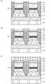
- the thin films 112a, 113a, and 114a are patterned so as to correspond to the sub-pixels by, for example, PR / PE. Thereby, as shown in FIG. 5A, the anode 112, the metal layer 113, and the hole injection layer 114 are formed.
- F As shown in FIG.
- a bank forming layer 115a for the bank 115 is formed on the insulating layer 111, the anode 112, the metal layer 113, and the hole injection layer 114, and shown in FIG.
- the bank formation layer 115a existing on the hole injection layer 114 is removed.
- an organic material is used as the material of the bank 115.
- the bank formation layer 115a is formed by, for example, a spin coat method.
- the removal of the bank formation layer 115a on the hole injection layer 114 is performed by PR / PE, for example.
- the bank 115 may be a striped line bank that extends only in the column direction or the row direction, or may be a pixel bank that extends in the column direction and the row direction and has a planar shape in a plane shape.
- a line bank first, after a pixel restricting layer (which is an insulating material) is provided between the anodes 112 adjacent to each other in the extending direction of the line bank, a bank forming layer is formed.
- the hole transport layer 116 is formed in the recess 115 b between the banks 115.
- polyfluorene is used as the material of the hole transport layer 116.
- the formation is performed, for example, by filling the recess 115b with an ink containing polyfluorene and then drying (for example, a thickness of 10 nm).
- an organic EL layer 117 is formed in the recess 115 b between the banks 115.
- the organic EL layer 117 is formed, for example, by filling the recess 115b with ink containing the above-described material and then drying it.
- an inkjet method is used for ink filling. Drying is performed, for example, under reduced pressure, and then baking is performed if necessary (for example, a thickness of 45 nm).
- the method for filling the recess 115b with ink is not limited to the inkjet method, and may be a dispenser method, a nozzle coating method, a spin coating method, intaglio printing, letterpress printing, or the like.
- an electron transport layer 118 is formed on the bank 115 and the organic EL layer 117 so as to cover the bank 115 and the organic EL layer 117.
- an oxadiazole derivative is used as the material of the electron transport layer 118.
- a vapor deposition method can be used (for example, a thickness of 35 nm).
- a cathode 119 is formed on the upper surface of the electron transport layer 118.
- indium tin oxide is used as the material of the cathode 119.
- plasma deposition can be used (for example, a thickness of 35 nm).
- the sealing layer 120 is formed on the upper surface of the cathode 119.
- silicon nitride is used as the material of the sealing layer 120.
- a chemical vapor deposition method (CVD method) can be used (for example, a thickness of 660 nm).
- CVD method chemical vapor deposition method
- the formation of the thin film 112a for the anode 112, the thin film 113a for the metal layer 113, and the thin film 114a for the hole injection layer 114 will be described. These thin films are performed using a thin film forming apparatus. Hereinafter, the thin film forming apparatus will be described, and then the formation of each thin film will be described.
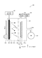
- the thin film forming apparatus 200 uses, for example, a magnetron sputtering apparatus as shown in FIG.
- the thin film forming apparatus 200 includes a vacuum vessel 201, a substrate holding unit 202 and a target holding unit 203 provided in the vacuum vessel 201, and turbo molecules for exhausting the inside of the vacuum vessel 201 into a vacuum via a pipe 204a.
- a pump 204 an oxygen gas supply unit 205 for supplying oxygen gas into the vacuum vessel 201, an inert gas supply unit 206 for supplying an inert gas (eg, argon) into the vacuum vessel 201, and plasma Plasma generating means 207 for generating a target, a magnet 208 for forming a desired magnetron magnetic field on the surface of the target member 210, a substrate-side space 201a in which the substrate holder 202 exists in the vacuum vessel 201, and the target holding Shutter 2 for dividing into two spaces, the target side space 201b where the portion 203 exists ; And a 9.
- an oxygen gas supply unit 205 for supplying oxygen gas into the vacuum vessel 201
- an inert gas supply unit 206 for supplying an inert gas (eg, argon) into the vacuum vessel 201
- plasma Plasma generating means 207 for generating a target
- a magnet 208 for forming a desired magnetron magnetic field on the surface of the target member 210
- the substrate holding unit 202 is a TFT substrate 110 which is an object on which a thin film is formed (in FIG. 8, before the thin film 113a for the metal layer 113 is formed and after the thin film 112a for the anode 112 is formed).
- This is a flat plate for holding the TFT substrate 110 in this state, and functions as a ground electrode during sputtering.
- the target holding unit 203 is a flat plate for holding the target member 210 and functions as a power input electrode during sputtering.
- Plasma is generated in the vacuum container 201 by the plasma generating means 207 between the substrate holding unit 202 and the target holding unit 203.
- the magnet 208 is arranged on the side of the target holding unit 203 opposite to the side where the target member 210 is installed, and is scanned back and forth in the direction indicated by the arrow in FIG.
- the shutter 209 can make the substrate-side space 201a and the target-side space 201b continuous or divided by opening and closing. For this reason, the target member 210 can be exchanged in a state where the shutter 209 is closed (a state where the vacuum in the substrate side space 201a is maintained).
- the thin film forming apparatus is not limited to a magnetron sputtering apparatus, and may be, for example, an ion beam sputtering apparatus.
- the turbo molecular pump 204 is operated to evacuate the vacuum vessel 201, and then argon is introduced from the inert gas supply unit 206 to operate the plasma generating means 207.
- the argon nuclei converted into plasma collide with the target member 210, and the sputtered sputtered particles adhere (deposit) to the surface of the insulating layer 111 of the TFT substrate 110, thereby forming a thin film 112a made of an aluminum alloy.
- B Formation of the thin film 113a for the metal layer 113
- the vacuum vessel 201 is maintained in a vacuum state or filled with argon, the shutter 209 is closed, and the target member 210 is closed. Is replaced with tungsten for the metal layer 113.
- the target member 210 can be exchanged without the thin film 112a for the anode 112 formed on the TFT substrate 110 being in contact with oxygen (without being oxidized).
- the target-side space 201b is again exhausted by the turbo molecular pump 204, and then the shutter 209 is opened. Then, the inert gas supply unit 206 fills the vacuum container 201 with argon gas and operates the plasma generating means 207 (see FIG. 8).
- a thin film (tungsten layer) 113a for the metal layer 113 is formed on the thin film 112a for the anode 112.
- the vacuum vessel 201 is filled with argon gas, and the thin film 112a for the anode 112 does not come into contact with oxygen and is less likely to be oxidized.
- C Formation of Thin Film 114 a for Hole Injection Layer 114
- the hole injection layer 114 is made of an oxide obtained by oxidizing the metal (tungsten) constituting the metal layer 113, it is not necessary to replace the target member 210, and the hole injection layer can be efficiently formed.
- a thin film 114a for 114 can be formed.
- the plasma generating means 207 is operated.
- the inside of the vacuum vessel 201 is in an oxygen atmosphere, but since the thin film 112a for the anode 112 is covered with the thin film 113a of the metal layer 113, the thin film 112a for the anode 112 is rarely oxidized.
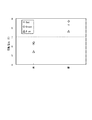
- FIG. 9 is a diagram showing the relationship between the presence / absence of a metal layer and the drive voltage.
- each pixel has sub-pixels of red (“Red” in the drawing), green (“Green” in the drawing), and blue (“Blue” in the drawing).
- a display panel having a metal layer in a pixel (“Yes” in the figure) and a display panel having red, green, and blue subpixels and having no metal layer in each subpixel (“No” in the figure) The voltage at the time of driving was measured for each display panel.
- the metal layer uses tungsten
- the anode uses an aluminum alloy.
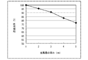
- FIG. 10 is a diagram showing the relationship between the thickness of the metal layer and the light transmission efficiency.
- FIG. 10 shows the light transmission efficiency of metal layers of 2 nm, 3 nm, 4 nm, and 5 nm with reference to a metal layer having a thickness of 1 nm.
- the metal layer is formed on the upper surface of the anode, and the organic EL layer is formed on the upper surface (or above) of the metal layer. For this reason, the light emitted from the organic EL layer toward the anode is transmitted through the metal layer and reflected by the anode, and further passes through the metal layer, the organic EL layer, the cathode, etc. Emitted. For this reason, a metal containing aluminum, which is a highly reflective material, is used for the anode, and the metal layer is also required to have high translucency.
- the light transmission efficiency decreases as the metal layer becomes thicker.
- the thickness is 2 nm, 95% can be maintained with respect to the thickness of 1 nm.
- the thickness is 3 nm, 90% can be maintained with respect to the thickness of 1 nm.
- the thickness is 4 nm, 80% or more can be maintained with respect to the thickness of 1 nm.
- the thickness of the metal layer is preferably 4 nm or less.
- FIG. 11 is a diagram showing the relationship between the thickness of the metal layer and the specific resistance.
- the specific resistance value in FIG. 11 is the specific resistance value of the bus bar portion. That is, it is a specific resistance value at a portion where an anode, a metal layer, a metal oxide layer, and a cathode are sequentially formed.
- Aluminum alloy is used for the anode
- tungsten is used for the metal
- tungsten oxide is used for the metal oxide layer
- indium tin oxide is used for the cathode.
- the specific resistance is considered to be constant regardless of the thickness because the same material is used for the metal layer. However, when the metal layer is as thin as 1 nm, the specific resistance is higher than that of 2 nm or 3 nm. This is considered that when the thickness of the metal layer is as thin as 1 nm, oxygen in the metal oxide layer and oxygen in the metal oxide layer reach the anode beyond the metal layer, and the surface of the anode is oxidized.
- the thickness is preferably 1 nm or more, and if it is 2 nm or more, it is considered that the oxidation of the anode can be prevented.
- FIG. 12 is a diagram showing the relationship between applied voltage and current density at each thickness of the metal layer.
- the subpixel having a metal layer with a thickness of 1 nm has a higher current density than the subpixel having a metal layer with a thickness of 2 nm and 3 nm even when a voltage as high as 5 V is applied. Absent.
- the hole injecting and transporting property is better than that of the metal layer having a thickness of 1 nm.
- the thickness of the metal layer is preferably 2 nm or more from the viewpoint of hole injection / transport properties. 7).
- Metal Layer and Metal Oxide Layer The metal layer and the metal oxide layer utilize tungsten in the embodiment. However, if the metal layer is a thin film containing a metal constituting the metal oxide layer, the replacement of the target member can be reduced when the thin film is formed, and the metal layer and the metal oxide layer can be formed efficiently. .
- tungsten may be used as a metal constituting the metal oxide layer, and the metal layer may be composed of an alloy containing tungsten.
- a metal constituting the metal oxide layer for example, a nickel tungsten alloy (NiW) may be used, and the metal layer may be composed of tungsten or nickel alone, or the metal layer may be composed of a nickel tungsten alloy.
- the metal layer may be composed of a nickel tungsten molybdenum alloy or a tungsten molybdenum alloy containing another metal (for example, molybdenum) that is not contained in the metal of the metal oxide layer.
- the above embodiment is an example used for easily explaining the configuration, operation, and effect of one embodiment of the present invention.
- the content of the present invention is not limited to the above embodiment.
- the light emitting device is described as a color display device.
- the light-emitting device according to one embodiment of the present invention can be applied to, for example, a single-color display device.
- the method for manufacturing a light-emitting device according to one embodiment of the present invention can be applied to such a method for manufacturing a light-emitting device.
- One embodiment of a light-emitting device may be a lighting device having a light-modulating / color-adjusting function by using a subpixel structure of a display device.
- the method for manufacturing a light-emitting device according to one embodiment of the present invention can also be applied to a method for manufacturing a light-emitting device as such a lighting device. In this case, it is not necessary to increase the number of pixels as in the EL display device.
- the light-emitting device in the embodiment includes an anode, a metal layer, a metal oxide layer (hole injection layer), a hole transport layer, an EL layer, an electron transport layer, a cathode, and a sealing layer.
- a light-emitting device is characterized by a stacked structure of an anode, a metal layer formed on the upper surface of the anode, and a metal oxide layer (hole injection layer) formed on the upper surface of the metal layer.
- a hole transport layer, an electron transport layer, and a sealing layer may not be provided, and structures other than those described in the light-emitting device in the embodiment, for example, an electron injection layer and a color filter layer May be provided.
- the method for manufacturing a light-emitting device according to one embodiment of the present invention can also be applied to a method for manufacturing a light-emitting device having such a structure.
- the first electrode serves as an anode and the second electrode serves as a cathode, and the metal oxide layer functions as a hole injection layer.
- the light-emitting device according to one embodiment of the present invention may be a light-emitting device in which the first electrode serves as a cathode and the second electrode serves as an anode, and the metal oxide layer functions as an electron injection layer or the like. .
- the method for manufacturing a light-emitting device according to one embodiment of the present invention can be applied to such a method for manufacturing a light-emitting device.
- the metal layer and metal oxide layer in the thin film embodiment are formed by sputtering. However, even in thin film forming methods such as vacuum deposition and ion plating, it is not necessary to exchange materials, and these methods can also be applied.
- the thin film forming method is a forming method in which atoms or molecules of the material constituting the thin film are formed by flying at a speed higher than the speed of sound.
- the EL layer in the embodiment is formed of an organic material, but the light-emitting device according to one embodiment of the present invention is formed on the anode, the metal layer formed on the upper surface of the anode, and the upper surface of the metal layer.
- the EL layer may be made of an inorganic material.
- the EL layer has a feature in a laminated structure with a metal oxide layer (hole injection layer).
- the method for manufacturing a light-emitting device according to one embodiment of the present invention can also be applied to a method for manufacturing a light-emitting device having such an EL layer.
- the light-emitting device and the method for manufacturing the light-emitting device according to one embodiment of the present invention can be used for efficiently manufacturing the light-emitting device.
- TFT substrate Substrate (TFT substrate) 111 Insulating layer 112 Anode 113 Metal layer 114 Metal oxide layer (hole injection layer) 115 Bank 116 Hole Transport Layer 117 Organic EL Layer 118 Electron Transport Layer 119 Cathode 120 Sealing Layer 200 Thin Film Forming Apparatus
Landscapes
- Electroluminescent Light Sources (AREA)
Abstract
発光装置は、アルミニウム又は銀を含有する第1電極と、第1電極の上面に形成された金属層と、金属層の上面に形成され且つ遷移金属を含有する金属の酸化物からなる金属酸化物層と、金属酸化物層上に形成されたEL層と、EL層上に形成された第2電極とを備え、金属層は、遷移金属と同じ金属を含有する。
Description
本発明は、EL層を備える発光装置および発光装置の製造方法に関する。
発光装置として、陽極とEL層との間に正孔注入層が配され、発光効率を向上させたものがある。トップエミッション型の発光装置は、例えば、陽極には高反射材料(合金を含む。)が、正孔注入層には遷移金属(合金を含む。)の酸化物がそれぞれ利用される。
正孔注入層は、遷移金属を含有する金属のターゲット部材を用いて、酸素プラズマを利用した反応性スパッタ法により形成される。具体的には、ターゲット部材を内部に収納する真空容器内にアルゴンガスおよび酸素ガスを供給してスパッタリングしている。
これによって、ターゲット部材の表面が酸化し、この表面の酸化物がスパッタされて、金属酸化物層が陽極上に形成される。
しかしながら、酸素プラズマは極めて金属を酸化させ易い特性を有するため、反応性スパッタ法で正孔注入層を形成すると、例えば、陽極としてアルミニウムや銀を利用した場合、陽極の表面が酸化されてしまう。
陽極の表面が酸化されてしまうと、陽極の表面が黒化して光反射機能が低下し、発光装置の発光輝度が低下する。また、アルミニウムが酸化した場合は、陽極が高電気抵抗化し、発光に必要な量の電流が流れなくなり、さらに発光装置の発光輝度が低下する。なお、発光に必要な量の電流を流すために、陽極と陰極との間により大きな電圧を印加すると、発光装置(EL層)が短寿命化する。
これに対して、例えば、ニッケル(Ni)からなる金属層を陽極上面に形成して、陽極が酸化するのを防ぐ技術が提案されている(例えば、特許文献1)。
しかしながら、上記ニッケル層は、メッキ溶液を利用した無電解メッキ法により形成されている。このため、浸漬後の溶液の除去等の作業が必要となり、ニッケル層の形成に時間と手間とを要してしまい、発光装置の製造プロセスが煩雑化する。
本発明は、上記の課題に鑑み、アルミニウム又は銀を含有する第1電極の表面に、酸化防止用の金属層を容易に形成することができる発光装置および発光装置の製造方法を提供することを目的とする。
上記目的を達成するため、本発明の一態様に係る発光装置は、アルミニウム又は銀を含有する第1電極と、前記第1電極の上面に形成された金属層と、前記金属層の上面に形成され且つ遷移金属を含有する金属の酸化物からなる金属酸化物層と、前記金属酸化物層上に形成されたEL層と、前記EL層上に形成された第2電極とを備え、前記金属層は、前記遷移金属と同じ金属を含有する。
本発明の一態様に係る発光装置は、金属層が金属酸化物層を構成する遷移金属と同じ金属を含有するため、金属層を形成する際に、金属酸化物層用の金属以外の金属層専用の金属を準備することが少なく、金属層を容易に設けることができる。
以下、本発明の一態様に係る発光装置および発光装置の製造方法について、図面を参照しながら説明する。
[本発明の一態様の概要]
本発明の一態様に係る発光装置は、アルミニウム又は銀を含有する第1電極と、前記第1電極の上面に形成された金属層と、前記金属層の上面に形成され且つ遷移金属を含有する金属の酸化物からなる金属酸化物層と、前記金属酸化物層上に形成されたEL層と、前記EL層上に形成された第2電極とを備え、前記金属層は、前記遷移金属と同じ金属を含有する。これにより、金属層を容易に設けることができる。
[本発明の一態様の概要]
本発明の一態様に係る発光装置は、アルミニウム又は銀を含有する第1電極と、前記第1電極の上面に形成された金属層と、前記金属層の上面に形成され且つ遷移金属を含有する金属の酸化物からなる金属酸化物層と、前記金属酸化物層上に形成されたEL層と、前記EL層上に形成された第2電極とを備え、前記金属層は、前記遷移金属と同じ金属を含有する。これにより、金属層を容易に設けることができる。
前記金属層の厚みが、1nm以上、4nm以下の範囲内にある。これにより、第1電極の酸化を抑制でき、しかも、高い光透過性を有する金属層が得られる。前記金属層の厚みが、2nm以上である。これにより、駆動時の比抵抗を小さくできる。前記金属層の厚みが、3nm以下である。これにより、より高い光の透過性を有する金属層が得られる。
前記金属層は、前記金属酸化物層の前記遷移金属を含有する金属と同じ金属により構成されている。これにより、金属層を効率よく設けることができる。前記遷移金属はタングステンである。これにより、金属酸化物層を正孔注入層とした場合に、正孔注入特性を向上させることができる。
本発明の一態様に係る発光装置の製造方法は、アルミニウム又は銀を含有する第1電極を基板に形成し、遷移金属を含有する金属層を前記第1電極の上面に薄膜成形法にて形成し、前記遷移金属と同じ金属を含有する金属の酸化物からなる金属酸化物層を前記金属層の上面に薄膜成形法にて形成し、EL層を前記金属酸化物層上に形成し、第2電極を前記EL層上に形成する。これにより、金属層を容易に設けることができる。
また、前記金属層は、1nm以上、4nm以下の範囲内の厚みに形成される。これにより、第1電極の酸化を抑制でき、しかも、高い光透過性を有する金属層が得られる。
[実施形態]
実施形態では、発光装置の例として、発光色が複数あり、これらを混合させた混色光を発光して、画像(情報)を表示する有機EL表示装置について説明する。以下、図面を参照しながら、実施形態の有機EL表示装置1について説明する。
1.全体構成
実施形態に係る有機EL表示装置1の概略構成について、図1および図2を用いて説明する。
[実施形態]
実施形態では、発光装置の例として、発光色が複数あり、これらを混合させた混色光を発光して、画像(情報)を表示する有機EL表示装置について説明する。以下、図面を参照しながら、実施形態の有機EL表示装置1について説明する。
1.全体構成
実施形態に係る有機EL表示装置1の概略構成について、図1および図2を用いて説明する。
図1に示すように、有機EL表示装置1は、表示パネル10と、これに接続された駆動・制御部20とを備えている。表示パネル10は、有機材料の電界発光現象を利用した有機ELパネルである。
表示パネル10は、複数個のサブピクセルを有している。ここでは、図2に示すように、複数のサブピクセル(副画素部)10a,10b,10cは、X軸方向およびY軸方向に二次元配置されている。
なお、X軸方向は発光色の異なるサブピクセルが隣接する方向であり、Y軸方向は同じ発光色のサブピクセルが隣接する(並ぶ)方向であるが、この方向に限定するものではない。
実施形態においては、例えば、サブピクセル10aが赤色光(R)を出射する発光部であり、サブピクセル10bが緑色光(G)を出射する発光部であり、サブピクセル10cが青色光(B)を出射する発光部である。そして、隣接する3つのサブピクセル10a,10b,10cを以って1つのピクセル(画素部)が構成されている。
図1に戻って、駆動・制御部20は、複数(例えば4つである。)の駆動回路21,22,23,24と制御回路25とから構成されている。なお、有機EL表示装置1における表示パネル10と駆動・制御部20との配置関係については、図1の形態には限定されない。
ピクセルの構成については、図2に示すような3つのサブピクセル10a~10cの組み合わせからなる形態に限定されず、例えば、黄色光や黒色光等を出射するサブピクセルを、上記3色光をそれぞれ出射するサブピクセル10a~10cに加えた、4つ以上のサブピクセルを組み合わせて1つのピクセルを構成してもよい。
2.表示パネル10の概略構成
図3は、図2のA-A断面での構成を示す模式断面図である。
2.表示パネル10の概略構成
図3は、図2のA-A断面での構成を示す模式断面図である。
図3に示すように、表示パネル10は、TFT基板110をベースとして、その上に絶縁層111が積層されている。絶縁層111のZ軸方向上面は、略平坦となるように形成されている。なお、TFT基板110については、TFT層などの図示を省略し、簡略化した図としている。また、Z軸方向は表示パネル10の厚み方向である。
絶縁層111のZ軸方向上面には、陽極112、金属層113および正孔注入層114が順に積層形成されている。なお、ここでは、陽極が本発明の第1電極に相当し、正孔注入層が本発明の金属酸化物層に相当する。
次に、絶縁層111上および正孔注入層114のX軸方向両縁上を覆うように、バンク115が形成されている。バンク115は、サブピクセル10aにおける発光領域部分の開口を規定する。
バンク115により規定された開口内には、Z軸方向下側から順に、正孔輸送層116、有機EL層117が積層形成されている。有機EL層117上およびバンク115の頂面上を覆うように、電子輸送層118、陰極119および封止層120がこの順に形成されている。なお、ここでは、有機EL層117が本発明のEL層に相当し、陰極が本発明の第2電極に相当する。
ここでは、表示パネル10は、封止層120の上面に、各光色の発光部に対応したカラーフィルタを有するフィルタ層を有していないが、フィルタ層を樹脂層により封止層120に貼り付けるような構造であってもよい。
本実施形態に係る表示パネル10は、トップエミッション型の表示パネルであり、矢印のようにZ軸方向上向きの光を出射する。
なお、図3では、サブピクセル10aの構成だけを抜き出して図示しているが、他のサブピクセル10b,10cについても同様の構成を有する。なお、各サブピクセル10a,10b,10cで、有機EL層117を構成する発光材料が異なる。
3.各部の構成
(1)TFT基板110
TFT基板110は、基板と、当該基板のZ軸方向上面に形成されたTFT層とから構成されている。TFT層については、図示を省略しているが、ゲート、ソース、ドレインの3電極と、半導体層、パッシベーション層などを含み構成されている。
3.各部の構成
(1)TFT基板110
TFT基板110は、基板と、当該基板のZ軸方向上面に形成されたTFT層とから構成されている。TFT層については、図示を省略しているが、ゲート、ソース、ドレインの3電極と、半導体層、パッシベーション層などを含み構成されている。
TFT基板110の基板は、例えば、ガラス基板、石英基板、シリコン基板などの無機基板、硫化モリブデン、銅、亜鉛、アルミニウム、ステンレス、マグネシウム、鉄、ニッケル、金、銀などの金属基板、ガリウム砒素などの半導体基板、プラスチック基板等を用い形成されている。
プラスチック基板としては、熱可塑性樹脂、熱硬化性樹脂いずれの樹脂を用いてもよい。例えば、ポリエチレン、ポリプロピレン、エチレン-プロピレン共重合体、エチレン-酢酸ビニル共重合体(EVA)等のポリオレフィン、環状ポリオレフィン、変性ポリオレフィン、ポリ塩化ビニル、ポリ塩化ビニリデン、ポリスチレン、ポリアミド、ポリイミド(PI)、ポリアミドイミド、ポリカーボネート、ポリ-(4-メチルベンテン-1)、アイオノマー、アクリル系樹脂、ポリメチルメタクリレート、アクリル-スチレン共重合体(AS樹脂)、ブタジエン-スチレン共重合体、ポリオ共重合体(EVOH)、ポリエチレンテレフタレート(PET)、ポリブチレンテレフタレート、ポリエチレンナフタレート(PEN)、プリシクロヘキサンテレフタレート(PCT)等のポリエステル、ポリエーテル、ポリエーテルケトン、ポリエーテルスルホン(PES)、ポリエーテルイミド、ポリアセタール、ポリフェニレンオキシド、変形ポリフェニレンオキシド、ポリアリレート、芳香族ポリエステル(液晶ポリマー)、ポリテトラフルオロエチレン、ポリフッ化ビニリデン、その他フッ素系樹脂、スチレン系、ポリオレフィン系、ポリ塩化ビニル系、ポリウレタン系、フッ素ゴム系、塩素化ポリエチレン系等の各種熱可塑性エラストマー、エポキシ樹脂、フェノール樹脂、ユリア樹脂、メラミン樹脂、不飽和ポリエステル、シリコーン樹脂、ポリウレタン等、またはこれらを主とする共重合体、ブレンド体、ポリマーアロイ等が挙げられ、これらのうち1種、または2種以上を積層した積層体を用いることができる。
(2)絶縁層111
絶縁層111は、例えば、有機材料や無機材料により形成されている。有機材料としては、例えば、ポリイミド、ポリアミド、アクリル系、フェノール系樹脂などがある。無機材料としては、例えば、シリコンオキサイド(SiO2)、シリコンナイトライド(Si3N4)などがある。なお、絶縁層111は、バンク115等に有機材料を用いる場合、有機溶剤耐性を有することが好ましい。
(2)絶縁層111
絶縁層111は、例えば、有機材料や無機材料により形成されている。有機材料としては、例えば、ポリイミド、ポリアミド、アクリル系、フェノール系樹脂などがある。無機材料としては、例えば、シリコンオキサイド(SiO2)、シリコンナイトライド(Si3N4)などがある。なお、絶縁層111は、バンク115等に有機材料を用いる場合、有機溶剤耐性を有することが好ましい。
また、絶縁層111は、製造工程中において、エッチング処理、ベーク処理等が施されることがあるので、それらの処理に対して過度に変形や変質などを生じない高い耐性を有する材料を用い形成されることが望ましい。
(3)陽極112
本実施形態に係る表示パネル10は、トップエミッション型であるため、陽極112は、有機EL層117から発せられた光を陰極119側に反射させる反射機能を有している(所謂、反射電極でもある。)。
(3)陽極112
本実施形態に係る表示パネル10は、トップエミッション型であるため、陽極112は、有機EL層117から発せられた光を陰極119側に反射させる反射機能を有している(所謂、反射電極でもある。)。
具体的には、陽極112は、反射性の高い、アルミニウム(Al)または銀(Ag)を含有する金属から構成されている。このような金属としては、例えば、アルミニウム、銀、ACL(アルミニウム、コバルト、ランタンの合金)等のアルミニウム合金、APC(銀、パラジウム、銅の合金)やARA(銀、ルビジウム、金の合金)等の銀合金等がある。
なお、アルミニウムを含有する金属を用いた場合、銀を含有する金属を用いるよりも、コスト面および重量面において優れている。
(4)金属層113
金属層113は、遷移金属を含有する金属から構成されている。ここでの「遷移金属を含有する金属」の概念には、遷移金属に属する金属や、当該遷移金属に属する金属を含有する合金からなる金属が含まれる。なお、遷移金属とは、周期表の第3族元素から第11族元素までの間に存在する元素である。
(4)金属層113
金属層113は、遷移金属を含有する金属から構成されている。ここでの「遷移金属を含有する金属」の概念には、遷移金属に属する金属や、当該遷移金属に属する金属を含有する合金からなる金属が含まれる。なお、遷移金属とは、周期表の第3族元素から第11族元素までの間に存在する元素である。
金属層113を構成する金属は、後述の正孔注入層114を構成する遷移金属と同じ金属(遷移金属)を含有している。さらに、金属層113を構成する金属は、正孔注入層を構成する遷移金属と同じ金属(遷移金属)を主として含有するのが好ましい。さらに、金属層113を構成する金属は、正孔注入層を構成する金属(酸化されていない金属)と同じ金属であるのがより一層好ましい。
(5)正孔注入層114
正孔注入層114は、遷移金属を含有する金属の酸化物から構成されている。ここでの「遷移金属を含有する金属」の概念には、遷移金属に属する金属や、当該遷移金属に属する金属を含有する合金からなる金属が含まれる。
(5)正孔注入層114
正孔注入層114は、遷移金属を含有する金属の酸化物から構成されている。ここでの「遷移金属を含有する金属」の概念には、遷移金属に属する金属や、当該遷移金属に属する金属を含有する合金からなる金属が含まれる。
遷移金属の中でも、タングステン、モリブデン、ニッケル、チタン、バナジウム、クロム、マンガン、鉄、コバルト、ニオブ、ハフニウム、タンタル等は、酸化した後に高い正孔注入性を有するため好ましい。
特に、タングステン、モリブデン、ニッケルおよびこれらを含んだ合金は、酸化した後に高いインギャップ状態を有する為、正孔注入能力が他の遷移金属が酸化した場合に比べて大きい。このことにより表示パネル用の正孔注入層用の金属として好ましい。
さらに、正孔注入層114を遷移金属酸化物から構成する場合には、複数の酸化数をとる。これにより複数の準位をとることができ、その結果、正孔注入が容易になり駆動電圧を低減することができる。特に、酸化タングステン(WOX)を用いることが、正孔を安定的に注入し、且つ、正孔の生成を補助するという機能を有するという観点から望ましい。
(6)バンク115
バンク115は、例えば、有機材料や無機材料により形成されている。有機材料としては、例えば、アクリル系、ポリイミド、フェノール系樹脂などがある。無機材料としては、例えば、SiO2、Si3N4などがある。
(6)バンク115
バンク115は、例えば、有機材料や無機材料により形成されている。有機材料としては、例えば、アクリル系、ポリイミド、フェノール系樹脂などがある。無機材料としては、例えば、SiO2、Si3N4などがある。
バンク115は、表面に撥水性をもたせるために、表面がフッ素処理されてもよい。さらに、バンク115の構造については、図3に示すような一層構造だけでなく、二層以上の多層構造を採用することもできる。この場合には、層毎に上記材料を組み合わせることもできるし、層毎に無機材料と有機材料とを用いることもできる。
(7)正孔輸送層116
正孔輸送層116は、親水基を備えない高分子化合物を用い形成されている。例えば、ポリフルオレンやその誘導体、あるいはポリアリールアミンやその誘導体などの高分子化合物であって、親水基を備えないものなどを用いることができる。
(8)有機EL層117
有機EL層117は、正孔と電子とが注入され再結合されることにより励起状態が生成され発光する機能を有する。有機EL層117の形成に用いる材料は、湿式印刷法を用い製膜できる発光性の有機材料を用いることが必要である。
(7)正孔輸送層116
正孔輸送層116は、親水基を備えない高分子化合物を用い形成されている。例えば、ポリフルオレンやその誘導体、あるいはポリアリールアミンやその誘導体などの高分子化合物であって、親水基を備えないものなどを用いることができる。
(8)有機EL層117
有機EL層117は、正孔と電子とが注入され再結合されることにより励起状態が生成され発光する機能を有する。有機EL層117の形成に用いる材料は、湿式印刷法を用い製膜できる発光性の有機材料を用いることが必要である。
具体的には、例えば、特許公開公報(日本国・特開平5-163488号公報)に記載のオキシノイド化合物、ペリレン化合物、クマリン化合物、アザクマリン化合物、オキサゾール化合物、オキサジアゾール化合物、ペリノン化合物、ピロロピロール化合物、ナフタレン化合物、アントラセン化合物、フルオレン化合物、フルオランテン化合物、テトラセン化合物、ピレン化合物、コロネン化合物、キノロン化合物およびアザキノロン化合物、ピラゾリン誘導体およびピラゾロン誘導体、ローダミン化合物、クリセン化合物、フェナントレン化合物、シクロペンタジエン化合物、スチルベン化合物、ジフェニルキノン化合物、スチリル化合物、ブタジエン化合物、ジシアノメチレンピラン化合物、ジシアノメチレンチオピラン化合物、フルオレセイン化合物、ピリリウム化合物、チアピリリウム化合物、セレナピリリウム化合物、テルロピリリウム化合物、芳香族アルダジエン化合物、オリゴフェニレン化合物、チオキサンテン化合物、シアニン化合物、アクリジン化合物、8-ヒドロキシキノリン化合物の金属錯体、2-ビピリジン化合物の金属錯体、シッフ塩とIII族金属との錯体、オキシン金属錯体、希土類錯体などの蛍光物質で形成されることが好ましい。
(9)電子輸送層118
電子輸送層118は、陰極119から注入された電子を有機EL層117へ輸送する機能を有する。電子輸送層118は、例えば、オキサジアゾール誘導体(OXD)、トリアゾール誘導体(TAZ)、フェナンスロリン誘導体(BCP、Bphen)などを用い形成されている。
(10)陰極119
陰極119は、例えば、酸化インジウムスズ(ITO)、酸化インジウム亜鉛(IZO)などを用い形成される。本実施形態のように、トップエミッション型の表示パネル10の場合、陰極119は光透過性の材料で形成されることが必要となる。なお、光透過性については、高透過性を有することが好ましく、例えば、透過率が80%以上とすることが好ましい。
(11)封止層120
封止層120は、有機EL層117などの有機層が水分に晒されたり、空気に晒されたりすることを抑制する機能を有する。封止層120は、例えば、窒化シリコン(SiN)、酸窒化シリコン(SiON)などの材料を用い形成される。また、窒化シリコン、酸窒化シリコンなどの材料を用いて形成された層の上に、アクリル樹脂、シリコーン樹脂などの樹脂からなる封止樹脂層を設けてもよい。
(9)電子輸送層118
電子輸送層118は、陰極119から注入された電子を有機EL層117へ輸送する機能を有する。電子輸送層118は、例えば、オキサジアゾール誘導体(OXD)、トリアゾール誘導体(TAZ)、フェナンスロリン誘導体(BCP、Bphen)などを用い形成されている。
(10)陰極119
陰極119は、例えば、酸化インジウムスズ(ITO)、酸化インジウム亜鉛(IZO)などを用い形成される。本実施形態のように、トップエミッション型の表示パネル10の場合、陰極119は光透過性の材料で形成されることが必要となる。なお、光透過性については、高透過性を有することが好ましく、例えば、透過率が80%以上とすることが好ましい。
(11)封止層120
封止層120は、有機EL層117などの有機層が水分に晒されたり、空気に晒されたりすることを抑制する機能を有する。封止層120は、例えば、窒化シリコン(SiN)、酸窒化シリコン(SiON)などの材料を用い形成される。また、窒化シリコン、酸窒化シリコンなどの材料を用いて形成された層の上に、アクリル樹脂、シリコーン樹脂などの樹脂からなる封止樹脂層を設けてもよい。
封止層120は、トップエミッション型の表示パネル10の場合、光透過性の材料で形成されることが必要となる。
4.表示パネル10の製造方法
以下、表示パネルの製造方法を、各部の材料等を例示する実施例を使って説明する。
4.表示パネル10の製造方法
以下、表示パネルの製造方法を、各部の材料等を例示する実施例を使って説明する。
図4~図7は、表示パネル10の形成工程を説明するための工程図である。
(A)TFT基板110を準備し、図4(a)に示すように、TFT基板110上に絶縁層111を形成する。ここでは、絶縁層111用の材料として、例えば有機材料を利用する。形成方法は、例えばスピンコート法を利用して、絶縁層111用の材料を塗布する。塗布後、PR/PE(フォトレジスト/フォトエッチング)でパターニングする。これにより、TFT基板110のドレイン電極に対応する部分に開口を有する絶縁層111が形成される(例えば、厚さ4μm)。
(B)図4(b)に示すように、絶縁層111上に陽極112用の薄膜112aを形成する。ここでは、陽極112の材料として、例えばアルミニウム合金(ここではACLである。)を利用し、薄膜112aは例えばスパッタリングにより形成される(例えば、厚さ200nm)。
(C)図4(c)に示すように、薄膜112a上に金属層113用の薄膜113aを形成する。ここでは、金属層113の材料として、例えばタングステンを利用する。薄膜113aは、スパッタリングにより形成される(例えば、厚さ3nm)。
(D)図4(d)に示すように、薄膜113a上に正孔注入層114用の薄膜114aを形成する。ここでは、正孔注入層114の材料として、遷移金属としてタングステンを用いた酸化タングステンを利用する。
(A)TFT基板110を準備し、図4(a)に示すように、TFT基板110上に絶縁層111を形成する。ここでは、絶縁層111用の材料として、例えば有機材料を利用する。形成方法は、例えばスピンコート法を利用して、絶縁層111用の材料を塗布する。塗布後、PR/PE(フォトレジスト/フォトエッチング)でパターニングする。これにより、TFT基板110のドレイン電極に対応する部分に開口を有する絶縁層111が形成される(例えば、厚さ4μm)。
(B)図4(b)に示すように、絶縁層111上に陽極112用の薄膜112aを形成する。ここでは、陽極112の材料として、例えばアルミニウム合金(ここではACLである。)を利用し、薄膜112aは例えばスパッタリングにより形成される(例えば、厚さ200nm)。
(C)図4(c)に示すように、薄膜112a上に金属層113用の薄膜113aを形成する。ここでは、金属層113の材料として、例えばタングステンを利用する。薄膜113aは、スパッタリングにより形成される(例えば、厚さ3nm)。
(D)図4(d)に示すように、薄膜113a上に正孔注入層114用の薄膜114aを形成する。ここでは、正孔注入層114の材料として、遷移金属としてタングステンを用いた酸化タングステンを利用する。
薄膜114aは、上記の薄膜113aの形成と同じターゲット部材で、酸素プラズマ雰囲気中でスパッタリングにより形成される(例えば、厚さ10nm)。なお、金属層113用の薄膜113aと正孔注入層114用の薄膜114aを成形する薄膜成形装置について後述する。
(E)薄膜112a,113a,114aに対して、例えばPR/PEにより、各サブピクセルに対応するようにパターニングする。これにより、図5(a)に示すように、陽極112、金属層113および正孔注入層114が形成される。
(F)図5(b)に示すように、絶縁層111、陽極112、金属層113および正孔注入層114上にバンク115用のバンク形成層115aを形成し、図5(c)に示すように、正孔注入層114上に存するバンク形成層115aを除去する。
(E)薄膜112a,113a,114aに対して、例えばPR/PEにより、各サブピクセルに対応するようにパターニングする。これにより、図5(a)に示すように、陽極112、金属層113および正孔注入層114が形成される。
(F)図5(b)に示すように、絶縁層111、陽極112、金属層113および正孔注入層114上にバンク115用のバンク形成層115aを形成し、図5(c)に示すように、正孔注入層114上に存するバンク形成層115aを除去する。
ここでは、バンク115の材料として、例えば有機材料を利用する。バンク形成層115aは、例えばスピンコート法により形成される。正孔注入層114上のバンク形成層115aの除去は、例えばPR/PEで行う。
バンク115は、列方向または行方向にだけ伸長するストライプ状のラインバンクであってもよいし、列方向および行方向に伸長し平面形状が井桁状のピクセルバンクであってもよい。なお、ラインバンクの場合、まず、ラインバンクの伸長する方向に隣接する陽極112間に画素規制層(絶縁材料である)が設けられた後、バンク形成層が形成される。
(G)図6(a)に示すように、バンク115間の凹部115bに正孔輸送層116を形成する。ここでは、正孔輸送層116の材料として、ポリフルオレンが利用されている。形成は、例えば、ポリフルオレンを含むインクを凹部115bに充填した後、乾燥させることによって行われる(例えば、厚さ10nm)。
(H)図6(b)に示すように、バンク115間の凹部115bに有機EL層117を形成する。有機EL層117は、例えば、上記した材料を含むインクを凹部115b内に充填した後、乾燥させることによって、形成される。
(G)図6(a)に示すように、バンク115間の凹部115bに正孔輸送層116を形成する。ここでは、正孔輸送層116の材料として、ポリフルオレンが利用されている。形成は、例えば、ポリフルオレンを含むインクを凹部115bに充填した後、乾燥させることによって行われる(例えば、厚さ10nm)。
(H)図6(b)に示すように、バンク115間の凹部115bに有機EL層117を形成する。有機EL層117は、例えば、上記した材料を含むインクを凹部115b内に充填した後、乾燥させることによって、形成される。
インクの充填は、例えばインクジェット法が利用される。乾燥は、例えば減圧下で行われ、その後、必要があればベーク処理する(例えば、厚さ45nm)。なお、インクを凹部115bに充填する方法は、インクジェット法に限定されず、ディスペンサー法、ノズルコート法、スピンコート法、凹版印刷、凸版印刷等であってもよい。
(I)図7(a)に示すように、バンク115および有機EL層117を覆うように、電子輸送層118をバンク115および有機EL層117上に形成する。ここでは、電子輸送層118の材料として、オキサジアゾール誘導体が利用されている。形成は、例えば蒸着法を利用できる(例えば、厚さ35nm)。
(J)図7(b)に示すように、電子輸送層118の上面に陰極119を形成する。ここでは、陰極119の材料として、例えば酸化インジウムスズが利用されている。形成は、例えばプラズマ蒸着を利用できる(例えば、厚さ35nm)。
(K)図7(c)に示すように、陰極119の上面に封止層120を形成する。ここでは、封止層120の材料として、例えば窒化シリコンが利用されている。形成は、例えば、化学気相堆積法(CVD法)を利用できる(例えば、厚さ660nm)。
5.薄膜形成について
陽極112用の薄膜112a、金属層113用の薄膜113aおよび正孔注入層114用の薄膜114aの形成について説明する。これらの薄膜は、薄膜形成装置を利用して行う。以下、薄膜形成装置について説明し、その後、各薄膜の形成について説明する。
(1)薄膜形成装置の構成
薄膜形成装置200は、図8に示すように、例えば、マグネトロンスパッタ装置を利用している。
(I)図7(a)に示すように、バンク115および有機EL層117を覆うように、電子輸送層118をバンク115および有機EL層117上に形成する。ここでは、電子輸送層118の材料として、オキサジアゾール誘導体が利用されている。形成は、例えば蒸着法を利用できる(例えば、厚さ35nm)。
(J)図7(b)に示すように、電子輸送層118の上面に陰極119を形成する。ここでは、陰極119の材料として、例えば酸化インジウムスズが利用されている。形成は、例えばプラズマ蒸着を利用できる(例えば、厚さ35nm)。
(K)図7(c)に示すように、陰極119の上面に封止層120を形成する。ここでは、封止層120の材料として、例えば窒化シリコンが利用されている。形成は、例えば、化学気相堆積法(CVD法)を利用できる(例えば、厚さ660nm)。
5.薄膜形成について
陽極112用の薄膜112a、金属層113用の薄膜113aおよび正孔注入層114用の薄膜114aの形成について説明する。これらの薄膜は、薄膜形成装置を利用して行う。以下、薄膜形成装置について説明し、その後、各薄膜の形成について説明する。
(1)薄膜形成装置の構成
薄膜形成装置200は、図8に示すように、例えば、マグネトロンスパッタ装置を利用している。
薄膜形成装置200は、真空容器201と、当該真空容器201内に設けられた基板保持部202およびターゲット保持部203と、真空容器201内を配管204aを介して真空状に排気するためのターボ分子ポンプ204と、真空容器201内に酸素ガスを供給するための酸素ガス供給部205と、真空容器201内に不活性ガス(例えば、アルゴン)を供給するための不活性ガス供給部206と、プラズマを発生させるためのプラズマ発生手段207と、ターゲット部材210の表面上に所望のマグネトロン磁場を形成するためのマグネット208と、真空容器201内を基板保持部202が存在する基板側空間201aとターゲット保持部203が存在するターゲット側空間201bとの2つの空間に分断するためのシャッター209とを具備する。
基板保持部202は、薄膜が形成される被形成体であるTFT基板110(図8では、金属層113用の薄膜113aが形成される前であって陽極112用の薄膜112aが形成された後の状態のTFT基板110を示している。)を保持するための平板であって、スパッタリングの際には接地電極として機能する。
一方、ターゲット保持部203は、ターゲット部材210を保持するための平板であって、スパッタリングの際には電力投入電極として機能する。基板保持部202とターゲット保持部203との間には、プラズマ発生手段207によって真空容器201内にプラズマが発生する。
マグネット208は、ターゲット保持部203の、ターゲット部材210が設置された側とは反対側に配置されており、ターゲット保持部203に対して図8の矢印に示す方向に往復して走査される。
シャッター209は、その開閉により、基板側空間201aとターゲット側空間201bとを連続させたり分断させたりすることが可能である。このため、シャッター209を閉めた状態(基板側空間201aの真空を維持した状態)で、ターゲット部材210を交換することができる。
なお、薄膜形成装置は、マグネトロンスパッタ装置に限定されず、例えばイオンビームスパッタ装置等であってもよい。
(2)薄膜形成について
(A)陽極112用の薄膜112aの形成
絶縁層111が形成されているTFT基板110を基板保持部202に設置し、陽極112用のターゲット部材210であるアルミニウム合金(ACL)をターゲット保持部203に設置する。
(2)薄膜形成について
(A)陽極112用の薄膜112aの形成
絶縁層111が形成されているTFT基板110を基板保持部202に設置し、陽極112用のターゲット部材210であるアルミニウム合金(ACL)をターゲット保持部203に設置する。
次に、ターボ分子ポンプ204を動作させて、真空容器201内を排気した後、不活性ガス供給部206からアルゴンを導入し、プラズマ発生手段207を動作させる。これにより、プラズマ化したアルゴン原子核がターゲット部材210と衝突して、スパッタされたスパッタ粒子がTFT基板110の絶縁層111の表面に付着(堆積)し、アルミニウム合金からなる薄膜112aが形成される。
(B)金属層113用の薄膜113aの形成
陽極112用の薄膜112aが形成されると、真空容器201内を真空状態又はアルゴンが充満した状態を維持し、シャッター209を閉鎖し、ターゲット部材210を金属層113用のタングステンに交換する。
(B)金属層113用の薄膜113aの形成
陽極112用の薄膜112aが形成されると、真空容器201内を真空状態又はアルゴンが充満した状態を維持し、シャッター209を閉鎖し、ターゲット部材210を金属層113用のタングステンに交換する。
これにより、TFT基板110上に形成された陽極112用の薄膜112aが酸素と触れることなく(酸化することなく)、ターゲット部材210を交換できる。
ターゲット部材210の交換を終えると、再び、ターゲット側空間201bをターボ分子ポンプ204により排気した後、シャッター209を開放する。そして、不活性ガス供給部206によりアルゴンガスを真空容器201内に充満させ、プラズマ発生手段207を動作させる(図8参照)。
これにより、陽極112用の薄膜112a上に、金属層113用の薄膜(タングステン層)113aが形成される。このとき、薄膜113aの形成中も、真空容器201は、アルゴンガスが充満されており、陽極112用の薄膜112aが酸素と触れることはなく、酸化するおそれが少ない。
(C)正孔注入層114用の薄膜114aの形成
金属層113用の薄膜113aが形成されると、真空容器201内に酸素ガス供給部205から酸素を真空容器201内に導入する。このとき、正孔注入層114は、金属層113を構成する金属(タングステン)を酸化した酸化物により構成しているため、ターゲット部材210を交換する必要がなく、効率的に、正孔注入層114用の薄膜114aを形成できる。
(C)正孔注入層114用の薄膜114aの形成
金属層113用の薄膜113aが形成されると、真空容器201内に酸素ガス供給部205から酸素を真空容器201内に導入する。このとき、正孔注入層114は、金属層113を構成する金属(タングステン)を酸化した酸化物により構成しているため、ターゲット部材210を交換する必要がなく、効率的に、正孔注入層114用の薄膜114aを形成できる。
この状態で、プラズマ発生手段207を動作させる。ここでは、酸素雰囲気下でアルゴンのプラズマを発生できればよく、アルゴン原子核がターゲット部材210をスパッタするほどの電圧は必要ない。このとき、真空容器201内は酸素雰囲気になるが、陽極112用の薄膜112aは金属層113の薄膜113aにより被覆されているので、陽極112用の薄膜112aが酸化するようなことも少ない。
また、金属層113の薄膜113aの表面は、酸素雰囲気下のため酸化するおそれがあるが、当該薄膜113aの表面に、金属層113の金属を酸化した正孔注入層114用の薄膜114aが形成されるため、薄膜113aの酸化が問題になることはない。
6.金属層の効果
(1)金属層の有無
図9は、金属層の有無と駆動電圧との関係を示す図である。
6.金属層の効果
(1)金属層の有無
図9は、金属層の有無と駆動電圧との関係を示す図である。
図9では、赤色(図中の「Red」である。)、緑色(図中の「Green」である。)および青色(図中の「Blue」である。)のサブピクセルを備え且つ各サブピクセルに金属層を有する表示パネル(図中の「有」である。)と、赤色、緑色および青色のサブピクセルを備え且つ各サブピクセルに金属層を有しない表示パネル(図中の「無」である。)とを製作して、各表示パネルについて駆動時の電圧を測定した。なお、ここでの金属層はタングステンを利用し、陽極にアルミニウム合金を利用している。
図9より、各色において駆動電圧が、金属層を有するサブピクセルの方が、有していないサブピクセルよりも低くなっていることが分る。これは、金属層を有することで、アルミニウムを利用している陽極の表面が酸化されず、逆に、金属層を有しないことで、陽極の表面が酸化されたものと考えられる。なお、陽極の表面が酸化されると、背景技術で説明したように、高電気抵抗化し、駆動電圧が高くなる。
(2)金属層の厚み
図10は、金属層の厚みと光の透過効率との関係を示す図である。
(2)金属層の厚み
図10は、金属層の厚みと光の透過効率との関係を示す図である。
図10は、1nmの厚みの金属層を基準にして、2nm、3nm、4nmおよび5nmの金属層の光の透過効率を示している。
金属層は陽極の上面に形成され、金属層の上面(又は上方)に有機EL層が形成されている。このため、有機EL層から陽極に向かって発せられた光は、金属層を透過して陽極で反射し、さらに、金属層、有機EL層、陰極等を通過して、発光部から外部へと出射される。このため、陽極には、高反射材料であるアルミニウムを含む金属が利用され、金属層も高い透光性が要求される。
図10に示すように、光の透過効率は、金属層が厚くなるに従って低下する。厚みが2nmでは、厚み1nmに対して95%を維持できる。厚みが3nmでは、厚み1nmに対して90%を維持できる。厚みが4nmでは、厚み1nmに対して80%以上を維持できる。
厚みが5nmでは、厚み1nmに対して77%程度となっており、実使用を考慮した場合、金属層の厚みは4nm以下が好ましい。
図11は、金属層の厚みと比抵抗との関係を示す図である。
図11の比抵抗値は、バスバー部分の比抵抗値である。つまり、陽極、金属層、金属酸化物層、陰極が順次形成された部分での比抵抗値である。なお、陽極にアルミニウム合金が、金属にタングステンが、金属酸化物層に酸化タングステンが、陰極に酸化インジウムスズがそれぞれ使用されている。
比抵抗は、金属層として同じ材料を使用しているため、厚みに関係なく、一定であると考えられる。しかしながら、金属層が1nmと薄くなると、厚みが2nmや3nmよりも比抵抗が高くなっている。これは、金属層の厚みが1nmと薄いと、金属酸化物層の形成時および金属酸化物層中の酸素が金属層を超えて陽極にまで達し、陽極の表面が酸化したものと考えられる。
従って、陽極の酸化を防止するには、金属層が有った方がよいが、その厚みが1nm以上であることが好ましく、2nm以上有れば、陽極の酸化を防止できると考えられる。
図12は、金属層の各厚みにおける、印加電圧と電流密度の関係を示す図である。
図では、縦軸の電流密度の数字が高い程、正孔が効率良く注入され、効率良く有機EL層に輸送されることを示す。つまり、印加電圧を高くしたときに、電流密度の増加分が大きいほど、正孔の注入性および輸送性(以下、単に、「正孔注入輸送性」ともいう。)が良好であることを示す。
図12では、厚みが1nmの金属層を有するサブピクセルは、電圧を5Vと高く印加しても、他の厚みが2nm、3nmの金属層を有するサブピクセルに比べて、電流密度が上昇していない。
これは、厚みが1nmの金属層を有するサブピクセルにおいて、陽極の表面が酸化したため、抵抗が高くなり、正孔注入輸送性が低下したものと考えられる。
一方、厚みが2nmの金属層を有する場合、厚みが3nmの金属層を有する場合とも、厚みが1nmの金属層よりも、正孔注入輸送性は良くなっており、厚みが3nmの金属層の方が厚み2nmの金属層よりも高い正孔注入輸送性を示す傾向にあるが、両者とも同レベルに有ると考えられる。以上のことから、正孔注入輸送性の観点からは、金属層の厚みは2nm以上が好ましい。
7.金属層および金属酸化物層
金属層および金属酸化物層は、実施形態ではタングステンを利用している。しかしながら、金属層は、金属酸化物層を構成する金属を含有する薄膜で有れば、薄膜形成する際に、ターゲット部材の交換を少なくでき、金属層および金属酸化物層を効率的に形成できる。
7.金属層および金属酸化物層
金属層および金属酸化物層は、実施形態ではタングステンを利用している。しかしながら、金属層は、金属酸化物層を構成する金属を含有する薄膜で有れば、薄膜形成する際に、ターゲット部材の交換を少なくでき、金属層および金属酸化物層を効率的に形成できる。
例えば、金属酸化物層を構成する金属としてタングステンを利用し、タングステンを含有する合金で金属層を構成してもよい。また、金属酸化物層を構成する金属として、例えば、ニッケルタングステン合金(NiW)を利用し、タングステン又はニッケルの単体で金属層を構成してもよいし、ニッケルタングステン合金で金属層を構成してもよいし、金属酸化物層の金属に含有されていない他の金属(例えばモリブデン)を含有した、ニッケルタングステンモリブデン合金やタングステンモリブデン合金で金属層を構成してもよい。
[変形例]
以上、本発明の一態様に係る発光装置およびその製造方法を具体的に説明してきたが、上記実施形態は、本発明の一態様の構成および作用・効果を分かり易く説明するために用いた例であって、本発明の内容は、上記の実施形態に限定されない。
1.発光装置
(1)適用
実施形態では、発光装置をカラーの表示装置として説明している。しかしながら、本発明の一態様に係る発光装置は、例えば単色表示の表示装置にも適用することができる。当然、このような発光装置の製造方法にも本発明の一態様に係る発光装置の製造方法を適用できる。
[変形例]
以上、本発明の一態様に係る発光装置およびその製造方法を具体的に説明してきたが、上記実施形態は、本発明の一態様の構成および作用・効果を分かり易く説明するために用いた例であって、本発明の内容は、上記の実施形態に限定されない。
1.発光装置
(1)適用
実施形態では、発光装置をカラーの表示装置として説明している。しかしながら、本発明の一態様に係る発光装置は、例えば単色表示の表示装置にも適用することができる。当然、このような発光装置の製造方法にも本発明の一態様に係る発光装置の製造方法を適用できる。
また、本発明の一態様に係る発光装置の一実施例は、表示装置のサブピクセル構造を利用して、調光・調色機能を有する照明装置としてもよい。当然、このような照明装置としての発光装置の製造方法にも本発明の一態様に係る発光装置の製造方法を適用できる。なお、この場合、EL表示装置程、高画素化する必要はない。
(2)構造
実施形態における発光装置は、陽極、金属層、金属酸化物層(正孔注入層)、正孔輸送層、EL層、電子輸送層、陰極、封止層を備えている。しかしながら、本発明の一態様に係る発光装置は、陽極と、陽極上面に形成された金属層と、金属層の上面に形成された金属酸化物層(正孔注入層)との積層構成に特徴を有するものであり、例えば、正孔輸送層、電子輸送層、封止層を備えていなくてもよいし、実施形態における発光装置で説明した以外の構造、例えば、電子注入層、カラーフィルタ層を備えてもよい。
(2)構造
実施形態における発光装置は、陽極、金属層、金属酸化物層(正孔注入層)、正孔輸送層、EL層、電子輸送層、陰極、封止層を備えている。しかしながら、本発明の一態様に係る発光装置は、陽極と、陽極上面に形成された金属層と、金属層の上面に形成された金属酸化物層(正孔注入層)との積層構成に特徴を有するものであり、例えば、正孔輸送層、電子輸送層、封止層を備えていなくてもよいし、実施形態における発光装置で説明した以外の構造、例えば、電子注入層、カラーフィルタ層を備えてもよい。
当然、このような構成をした発光装置の製造方法にも本発明の一態様に係る発光装置の製造方法を適用できる。
(3)電極
実施形態では、第1電極を陽極と、第2電極を陰極とそれぞれし、金属酸化物層を正孔注入層として機能させている。しかしながら、本発明の一態様に係る発光装置は、第1電極を陰極と、第2電極を陽極とそれぞれし、金属酸化物層を電子注入層等として機能させるような発光装置であってもよい。当然、このような発光装置の製造方法にも本発明の一態様に係る発光装置の製造方法を適用できる。
2.薄膜
実施形態における金属層および金属酸化物層はスパッタ法により形成している。しかしながら、真空蒸着、イオンプレーティング等の薄膜成形法においても、材料の交換が不要であり、これらの成形法においても適用できる。
(3)電極
実施形態では、第1電極を陽極と、第2電極を陰極とそれぞれし、金属酸化物層を正孔注入層として機能させている。しかしながら、本発明の一態様に係る発光装置は、第1電極を陰極と、第2電極を陽極とそれぞれし、金属酸化物層を電子注入層等として機能させるような発光装置であってもよい。当然、このような発光装置の製造方法にも本発明の一態様に係る発光装置の製造方法を適用できる。
2.薄膜
実施形態における金属層および金属酸化物層はスパッタ法により形成している。しかしながら、真空蒸着、イオンプレーティング等の薄膜成形法においても、材料の交換が不要であり、これらの成形法においても適用できる。
なお、ここでいう薄膜成形法は、薄膜を構成する材料の原子または分子が音速以上の速さで飛翔して形成される成形法である。
3.EL層
実施形態におけるEL層は、有機材料により構成されているが、本発明の一態様に係る発光装置は、陽極と、陽極上面に形成された金属層と、金属層の上面に形成された金属酸化物層(正孔注入層)との積層構成に特徴を有するものであり、EL層は、無機材料から構成されてもよい。当然、このようなEL層を有する発光装置の製造方法にも本発明の一態様に係る発光装置の製造方法を適用できる。
3.EL層
実施形態におけるEL層は、有機材料により構成されているが、本発明の一態様に係る発光装置は、陽極と、陽極上面に形成された金属層と、金属層の上面に形成された金属酸化物層(正孔注入層)との積層構成に特徴を有するものであり、EL層は、無機材料から構成されてもよい。当然、このようなEL層を有する発光装置の製造方法にも本発明の一態様に係る発光装置の製造方法を適用できる。
本発明の一態様に係る発光装置および発光装置の製造方法は、発光装置を効率よく製造するのに利用できる。
110 基板(TFT基板)
111 絶縁層
112 陽極
113 金属層
114 金属酸化物層(正孔注入層)
115 バンク
116 正孔輸送層
117 有機EL層
118 電子輸送層
119 陰極
120 封止層
200 薄膜形成装置
111 絶縁層
112 陽極
113 金属層
114 金属酸化物層(正孔注入層)
115 バンク
116 正孔輸送層
117 有機EL層
118 電子輸送層
119 陰極
120 封止層
200 薄膜形成装置
Claims (8)
- アルミニウム又は銀を含有する第1電極と、
前記第1電極の上面に形成された金属層と、
前記金属層の上面に形成され且つ遷移金属を含有する金属の酸化物からなる金属酸化物層と、
前記金属酸化物層上に形成されたEL層と、
前記EL層上に形成された第2電極と
を備え、
前記金属層は、前記遷移金属と同じ金属を含有する
発光装置。 - 前記金属層の厚みが、1nm以上、4nm以下の範囲内にある
請求項1に記載の発光装置。 - 前記金属層の厚みが、2nm以上である
請求項2に記載の発光装置。 - 前記金属層の厚みが、3nm以下である
請求項3に記載の発光装置。 - 前記金属層は、前記金属酸化物層の前記遷移金属を含有する金属と同じ金属により構成されている
請求項1~4の何れか1項に記載の発光装置。 - 前記遷移金属はタングステンである
請求項1~5の何れか1項に記載の発光装置。 - アルミニウム又は銀を含有する第1電極を基板に形成し、
遷移金属を含有する金属層を前記第1電極の上面に薄膜成形法にて形成し、
前記遷移金属と同じ金属を含有する金属の酸化物からなる金属酸化物層を前記金属層の上面に薄膜成形法にて形成し、
EL層を前記金属酸化物層上に形成し、
第2電極を前記EL層上に形成する
発光装置の製造方法。 - 前記金属層は、1nm以上、4nm以下の範囲内の厚みに形成される
請求項7に記載の発光装置の製造方法。
Applications Claiming Priority (2)
| Application Number | Priority Date | Filing Date | Title |
|---|---|---|---|
| JP2014033173 | 2014-02-24 | ||
| JP2014-033173 | 2014-02-24 |
Publications (1)
| Publication Number | Publication Date |
|---|---|
| WO2015125458A1 true WO2015125458A1 (ja) | 2015-08-27 |
Family
ID=53877980
Family Applications (1)
| Application Number | Title | Priority Date | Filing Date |
|---|---|---|---|
| PCT/JP2015/000711 Ceased WO2015125458A1 (ja) | 2014-02-24 | 2015-02-17 | 発光装置および発光装置の製造方法 |
Country Status (1)
| Country | Link |
|---|---|
| WO (1) | WO2015125458A1 (ja) |
Citations (4)
| Publication number | Priority date | Publication date | Assignee | Title |
|---|---|---|---|---|
| JP2011091093A (ja) * | 2009-10-20 | 2011-05-06 | Panasonic Corp | 有機el素子 |
| WO2012164797A1 (ja) * | 2011-06-03 | 2012-12-06 | パナソニック株式会社 | 薄膜形成方法、薄膜形成装置、表示パネルの製造方法、表示装置の製造方法、および発光装置の製造方法 |
| WO2013069274A1 (ja) * | 2011-11-10 | 2013-05-16 | パナソニック株式会社 | 有機表示パネル、有機表示装置、有機発光装置、それらの製造方法、および薄膜形成方法 |
| WO2013179360A1 (ja) * | 2012-06-01 | 2013-12-05 | パナソニック株式会社 | 発光素子およびそれを用いた表示装置 |
-
2015
- 2015-02-17 WO PCT/JP2015/000711 patent/WO2015125458A1/ja not_active Ceased
Patent Citations (4)
| Publication number | Priority date | Publication date | Assignee | Title |
|---|---|---|---|---|
| JP2011091093A (ja) * | 2009-10-20 | 2011-05-06 | Panasonic Corp | 有機el素子 |
| WO2012164797A1 (ja) * | 2011-06-03 | 2012-12-06 | パナソニック株式会社 | 薄膜形成方法、薄膜形成装置、表示パネルの製造方法、表示装置の製造方法、および発光装置の製造方法 |
| WO2013069274A1 (ja) * | 2011-11-10 | 2013-05-16 | パナソニック株式会社 | 有機表示パネル、有機表示装置、有機発光装置、それらの製造方法、および薄膜形成方法 |
| WO2013179360A1 (ja) * | 2012-06-01 | 2013-12-05 | パナソニック株式会社 | 発光素子およびそれを用いた表示装置 |
Similar Documents
| Publication | Publication Date | Title |
|---|---|---|
| JP5574456B2 (ja) | 発光素子とその製造方法、および発光装置 | |
| JP4659141B1 (ja) | 発光素子とその製造方法、および発光装置 | |
| CN108417600B (zh) | 有机el显示面板以及有机el显示面板的制造方法 | |
| JP6233888B2 (ja) | 有機発光デバイスとその製造方法 | |
| JP5543441B2 (ja) | 有機発光素子とその製造方法、有機表示パネル、有機表示装置 | |
| JP6789184B2 (ja) | 有機el表示パネル及び有機el表示パネルの製造方法 | |
| CN103053040A (zh) | 有机el元件 | |
| JP2016091841A (ja) | 有機発光デバイスと有機表示装置 | |
| JP2020030933A (ja) | 有機el表示パネル、及び有機el表示パネルの製造方法 | |
| WO2013179361A1 (ja) | 有機el素子、有機elパネル、有機el発光装置、および有機el表示装置 | |
| US9103017B2 (en) | Organic display panel, organic display device, organic light emitting device, method of manufacture of these, and thin film formation method | |
| JP5620495B2 (ja) | 発光素子、発光素子を備えた発光装置および発光素子の製造方法 | |
| WO2013051070A1 (ja) | 発光素子及び発光素子の製造方法 | |
| JP5861961B2 (ja) | 有機el素子とその製造方法 | |
| CN103843457A (zh) | 发光元件和发光元件的制造方法 | |
| JP2016110904A (ja) | 有機発光素子の製造方法および有機発光素子 | |
| JP6893020B2 (ja) | 有機el表示パネル及び有機el表示パネルの製造方法 | |
| JP5939564B2 (ja) | 有機el素子の製造方法 | |
| WO2015125458A1 (ja) | 発光装置および発光装置の製造方法 | |
| WO2012164797A1 (ja) | 薄膜形成方法、薄膜形成装置、表示パネルの製造方法、表示装置の製造方法、および発光装置の製造方法 | |
| JP2015103476A (ja) | 表示パネルおよびその製造方法 | |
| JP2016100150A (ja) | 有機発光素子の製造方法および有機発光素子 | |
| JP2018129264A (ja) | 有機el表示パネル、及び有機el表示パネルの製造方法 | |
| JP2017188345A (ja) | 発光パネルの製造方法、および、発光パネル | |
| JPWO2013051071A1 (ja) | 発光素子及び発光素子の製造方法 |
Legal Events
| Date | Code | Title | Description |
|---|---|---|---|
| 121 | Ep: the epo has been informed by wipo that ep was designated in this application |
Ref document number: 15751937 Country of ref document: EP Kind code of ref document: A1 |
|
| NENP | Non-entry into the national phase |
Ref country code: DE |
|
| 122 | Ep: pct application non-entry in european phase |
Ref document number: 15751937 Country of ref document: EP Kind code of ref document: A1 |
|
| NENP | Non-entry into the national phase |
Ref country code: JP |