WO2015125232A1 - 電流検出装置 - Google Patents
電流検出装置 Download PDFInfo
- Publication number
- WO2015125232A1 WO2015125232A1 PCT/JP2014/053900 JP2014053900W WO2015125232A1 WO 2015125232 A1 WO2015125232 A1 WO 2015125232A1 JP 2014053900 W JP2014053900 W JP 2014053900W WO 2015125232 A1 WO2015125232 A1 WO 2015125232A1
- Authority
- WO
- WIPO (PCT)
- Prior art keywords
- current
- detection
- conductive
- gmr
- conductive portion
- Prior art date
- Legal status (The legal status is an assumption and is not a legal conclusion. Google has not performed a legal analysis and makes no representation as to the accuracy of the status listed.)
- Ceased
Links
Images


Classifications
-
- G—PHYSICS
- G01—MEASURING; TESTING
- G01R—MEASURING ELECTRIC VARIABLES; MEASURING MAGNETIC VARIABLES
- G01R15/00—Details of measuring arrangements of the types provided for in groups G01R17/00 - G01R29/00, G01R33/00 - G01R33/26 or G01R35/00
- G01R15/14—Adaptations providing voltage or current isolation, e.g. for high-voltage or high-current networks
- G01R15/20—Adaptations providing voltage or current isolation, e.g. for high-voltage or high-current networks using galvano-magnetic devices, e.g. Hall-effect devices, i.e. measuring a magnetic field via the interaction between a current and a magnetic field, e.g. magneto resistive or Hall effect devices
- G01R15/207—Constructional details independent of the type of device used
-
- G—PHYSICS
- G01—MEASURING; TESTING
- G01R—MEASURING ELECTRIC VARIABLES; MEASURING MAGNETIC VARIABLES
- G01R15/00—Details of measuring arrangements of the types provided for in groups G01R17/00 - G01R29/00, G01R33/00 - G01R33/26 or G01R35/00
- G01R15/14—Adaptations providing voltage or current isolation, e.g. for high-voltage or high-current networks
- G01R15/20—Adaptations providing voltage or current isolation, e.g. for high-voltage or high-current networks using galvano-magnetic devices, e.g. Hall-effect devices, i.e. measuring a magnetic field via the interaction between a current and a magnetic field, e.g. magneto resistive or Hall effect devices
- G01R15/202—Adaptations providing voltage or current isolation, e.g. for high-voltage or high-current networks using galvano-magnetic devices, e.g. Hall-effect devices, i.e. measuring a magnetic field via the interaction between a current and a magnetic field, e.g. magneto resistive or Hall effect devices using Hall-effect devices
-
- G—PHYSICS
- G01—MEASURING; TESTING
- G01R—MEASURING ELECTRIC VARIABLES; MEASURING MAGNETIC VARIABLES
- G01R15/00—Details of measuring arrangements of the types provided for in groups G01R17/00 - G01R29/00, G01R33/00 - G01R33/26 or G01R35/00
- G01R15/14—Adaptations providing voltage or current isolation, e.g. for high-voltage or high-current networks
- G01R15/20—Adaptations providing voltage or current isolation, e.g. for high-voltage or high-current networks using galvano-magnetic devices, e.g. Hall-effect devices, i.e. measuring a magnetic field via the interaction between a current and a magnetic field, e.g. magneto resistive or Hall effect devices
- G01R15/205—Adaptations providing voltage or current isolation, e.g. for high-voltage or high-current networks using galvano-magnetic devices, e.g. Hall-effect devices, i.e. measuring a magnetic field via the interaction between a current and a magnetic field, e.g. magneto resistive or Hall effect devices using magneto-resistance devices, e.g. field plates
Definitions
- the present invention relates to a current detection device that detects a current flowing through a conductive member by detecting the strength of a magnetic field.
- a current detection device for example, a device that detects a current flowing in a plurality of current paths between a three-phase motor and an inverter using a current detection sensor provided in the vicinity of each current path is known (for example, see Patent Document 1.)
- the current detection device described in Patent Document 1 includes a plurality of flat current paths and a plurality of current detection sensors that detect currents flowing through the current paths.
- the current detection sensor is a magnetic flux detector such as an MR element that detects the strength of the magnetic field generated by the current flowing through the current path, and the current flowing through the current path based on the strength of the magnetic field detected by the magnetic flux detector. It has a current detection sensor main body for detecting a value.
- the magnetic flux detector is disposed near the center of the current path in the short direction through the current detection sensor body.
- the magnetic flux detector has a magnetic field detection direction that can detect a magnetic field in only one direction, and the magnetic field detection direction is a direction perpendicular to the direction of current flow and parallel to the short direction of the current path. It is.
- an object of the present invention is to provide a current detection device capable of widening a current detection range while suppressing an increase in size.
- the present invention includes a conductive member that supplies a current to be detected, and a detection sensor that detects the intensity of a magnetic field in a predetermined detection direction in the magnetic sensing unit, and the conductive member includes: A current detection device in which a part of the current flows in a parallel region parallel to the magnetic sensing unit along the detection direction is provided.
- the current detection device of the present invention it is possible to widen the current detection range while suppressing an increase in size.
- FIG. 2 is a sectional view taken along line AA in FIG. 1. It is sectional drawing which shows the 1st electric current detection unit in FIG. It is sectional drawing which shows one structural example of the electric current detection apparatus which concerns on the 2nd Embodiment of this invention. It is sectional drawing which shows the 1st electric current detection unit in FIG. It is sectional drawing which shows the 1st electric current detection unit which concerns on the modification of 2nd Embodiment. It is a top view which shows the example of 1 structure of the electric current detection apparatus which concerns on the 3rd Embodiment of this invention.
- FIG. 8 is a sectional view taken along line BB in FIG.
- a current detection apparatus according to a first embodiment of the present invention will be described with reference to FIGS.
- This current detection device is used, for example, to detect a current flowing in each phase of a U-phase, a V-phase, and a W-phase of a three-phase motor as a vehicle drive source.
- FIG. 1 is a perspective view showing a configuration example of the current detection device 11 according to the first embodiment of the present invention.
- 2 is a cross-sectional view taken along the line AA of FIG. 1, and specifically shows a cross section including the GMR element 41 perpendicular to the direction in which the currents I 1 , I 2 , and I 3 flow.
- the current detection device 11 includes conductive members 2a, 2b, and 2c that flow currents I 1 , I 2 , and I 3 to be detected, and a GMR sensor as a detection sensor that detects the intensity of a magnetic field in a predetermined detection direction in the magnetic sensing unit. 4a, 4b, 4c and a circuit board 3 on which GMR sensors 4a, 4b, 4c are mounted.
- the magnetic sensing part is configured by a giant magnetoresistive element (GMR element 41) having a giant magnetoresistive effect.
- the giant magnetoresistive effect can obtain a large change in electric resistance with respect to a small change in magnetic field. More specifically, for example, a magnetoresistive effect such as a Hall IC has a rate of change of electrical resistance of several percent, whereas a giant magnetoresistive element (GMR element) using this giant magnetoresistive effect The rate of change in resistance is as high as several tens of percent.
- the GMR element 41 is formed by laminating a ferromagnetic thin film such as cobalt (Co) and a nonmagnetic thin film such as copper (Cu).
- the GMR sensors 4a, 4b, 4c using the GMR element 41 can detect a current with high accuracy even for a small current.
- the current detection device 11 includes a GMR sensor 4a for the conductive member 2a, a GMR sensor 4b for the conductive member 2b, and a GMR sensor 4c for the conductive member 2c.
- the set of the conductive member 2a and the GMR sensor 4a is the first current detection unit 111
- the set of the conductive member 2b and the GMR sensor 4b is the second current detection unit 112
- the conductive member 2c and the GMR sensor 4c is a third current detection unit 113.
- the first to third current detection units 111 to 113 are arranged side by side on the mounting surface 3a on one side of the circuit board 3, and the conductive members 2a, 2b, and 2c are connected to the current I 1 as shown in FIG. , I 2 , I 3 are arranged so that their flowing directions are parallel to each other.
- the circuit board 3 is made of, for example, polychlorinated biphenyl (PCB) or glass epoxy.
- Each of the GMR sensors 4a, 4b, and 4c includes a sensor body 40, a GMR element 41, and a plurality of terminals 42 that are connected to the circuit board 3 by, for example, soldering (in FIG. 2, each of the GMR sensors 4a, 4b, and 4c). Only two are shown).
- the GMR element 41 has, for example, a square shape with a side of 10 ⁇ m and a thickness of about several ⁇ m.
- the GMR element 41 is located at the center of the sensor body 40, the magnetic field detection direction is parallel to the mounting surface 3a of the circuit board 3, and the currents I 1 and I 2 , I 3 is a direction perpendicular to the flowing direction of I 3 .
- the detection direction of the magnetic field of the GMR element 41 in each of the GMR sensors 4a, 4b, 4c is the same.
- the conductive member 2a is formed by bending a metal plate having a thickness of about 1.5 mm and extends in the direction in which the current I 1 flows. Further, the conductive member 2a has a width dimension perpendicular to the direction of current flow I 1 is about 15 mm, and has a housing portion 20 which GMR sensor 4a is accommodated in the central portion of the width direction.
- the parallel region 21a is indicated by a two-dot chain line.
- the parallel region 21a is a region where the direction of the magnetic field generated by the current flowing therethrough is orthogonal to the direction of detection of the magnetic field of the GMR element 41 at the position where the GMR element 41 is disposed, and the strength of the magnetic field is not detected by the GMR sensor 4a.
- the pair of first conductive portions 211 and 212 and the second conductive portion 22 are parallel to the mounting surface 3 a of the circuit board 3.
- cross section including the GMR element 41 perpendicular to the direction in which the currents I 1 , I 2 , and I 3 flow is simply referred to as “current direction orthogonal cross section”.
- the pair of first conductive portions 211 and 212 are disposed on both sides of the GMR sensor 4a in the detection direction of the GMR element 41, respectively.
- one first conductive portion 211 is disposed on the left side of the GMR sensor 4a
- the other first conductive portion 212 is disposed on the right side of the GMR sensor 4a.
- one first conductive portion 211 is referred to as a left first conductive portion 211
- the other first conductive portion 212 is referred to as a right first conductive portion 212.
- the second conductive portion 22 is disposed on one side of the GMR sensor 4 a so that the GMR sensor 4 a is positioned between the second conductive portion 22 and the circuit board 3 in a direction orthogonal to the detection direction of the GMR element 41.
- the second conductive portion 22 has the same width in the direction parallel to the detection direction of the GMR element 41 as the width in the direction parallel to the detection direction of the GMR element 41 in the GMR sensor 4a.
- the first conductive portion 211, the right first conductive portion 212, and the second conductive portion 22 are all set to have the same width in the direction parallel to the detection direction of the GMR element 41. It can be set according to the application of the detection device 11.
- the conductive member 2a includes a first connecting portion 231 that connects the left first conductive portion 211 and the second conductive portion 22, and a right first conductive portion 212 and the second conductive portion 22 in the cross section perpendicular to the current direction. It further has the 2nd connection part 232 which connects between.
- the first connection part 231 and the second connection part 232 are formed to be inclined with respect to the left first conductive part 211, the right first conductive part 212, and the second conductive part 22.
- the first connecting portion 231 may be formed so as to be orthogonal to the left first conductive portion 211 and the second conductive portion 22. The same applies to the second connecting portion 232.
- the left first conductive portion 211, the right first conductive portion 212, the second conductive portion 22, the first connecting portion 231, and the second connecting portion 232 are integrated by bending one metal plate. Is formed.
- the conductive member 2 a is not limited to this, for example, and does not have the first connection portion 231, and the left first conductive portion 211 and the second conductive portion 22 may be separated from each other, or the second connection portion 232.
- the right first conductive portion 212 and the second conductive portion 22 may be separated from each other.
- the second conductive portion 22, the first connecting portion 231, and the second connecting portion 232 constitute a part of the housing portion 20.
- FIG. 3 is a cross-sectional view showing the first current detection unit 111 in FIG. Note that the magnetic fields generated by the currents I 1 , I 2 , and I 3 and the magnetic fields detected by the GMR sensors 4a, 4b, and 4c are all the same in the first to third current detection units 111 to 113. Therefore, the first current detection unit 111 will be described below as an example.
- the current I 1 is applied to each of the left first conductive portion 211, the right first conductive portion 212, the second conductive portion 22, the first connecting portion 231, and the second connecting portion 232 in the cross section perpendicular to the current direction of the conductive member 2a. It flows in a distributed manner.
- the direction of the magnetic field generated by the current I 1 is clockwise.
- the magnetic field detection direction of the GMR element 41 is the direction from the right first conductive portion 212 toward the left first conductive portion 211 (arrow A in FIG. 3).
- the magnetic field B212 generated by the current I 1 flowing through the central portion of the right side first conductive unit 212, the direction of the arrangement position of the GMR element 41, toward the circuit board 3 side to the second conductive section 22 side It is orthogonal to the detection direction of the GMR element 41.
- a magnetic field is also generated by the current I 1 flowing through the first and second connecting portions 231 and 232, but for these magnetic fields, the intensity of the magnetic field in the direction along the detection direction of the GMR element 41 is GMR sensor 4a. Is detected.
- the intensity of the magnetic field detected by the GMR sensor 4a is the intensity of the magnetic field generated mainly by the current I 1 flowing through the second conductive portion 22 out of the magnetic field generated by the current I 1 flowing through the conductive member 2a.
- the conductive members 2a, 2b, and 2c It is not necessary to increase the distance between the GMR sensors 4a, 4b, and 4c, and it is possible to suppress an increase in the size of the current detection device 11, and the range of the intensity of the magnetic field that can be accurately detected is increased.
- the first conductive portions 211 and 212 and the second conductive portion 22 are integrally formed by bending a single metal plate, the first conductive portion 211 is formed. , 212 and the second conductive portion 22 are not separately prepared, and these metal members do not need to be combined, and workability can be improved and costs can be reduced.
- the current detection device 11 is a GMR sensor 4a, 4b having a GMR element 41 as a detection sensor for detecting the intensity of the magnetic field generated by the currents I 1 , I 2 , I 3 flowing through the conductive members 2a, 2b, 2c.
- a GMR sensor 4a, 4b having a GMR element 41 as a detection sensor for detecting the intensity of the magnetic field generated by the currents I 1 , I 2 , I 3 flowing through the conductive members 2a, 2b, 2c.
- 4c is used, for example, the sensitivity is higher than that of a sensor such as a Hall IC, and the intensity of the generated magnetic field can be accurately detected in a dynamic range (for example, 0.002 mT to 2.000 mT). .
- the conductive members 2a, 2b, and 2c are connected to the GMR sensors 4a, 4b, and 4c in the detection direction of the GMR element 41 in a cross section including the GMR element 41 perpendicular to the flowing direction of the currents I 1 , I 2 , and I 3 .
- the left first conductive portion 211 and the right first conductive portion 212 that are arranged alongside the GMR sensors 4a, 4b, and 4c along the detection direction of the GMR element 41 on both sides, and the detection of the GMR element 41 in the current direction orthogonal cross section
- the second conductive portion 22 disposed on one side of the GMR sensors 4a, 4b, 4c in a direction orthogonal to the direction, and the left first conductive portion 211 and the right first conductive portion 212 include a parallel region 21a.
- the currents I 1 , I 2 , and I 3 flowing through the conductive members 2a, 2b, and 2c are mainly dispersed in the left first conductive portion 211, the right first conductive portion 212, and the second conductive portion 22, respectively. Ru .
- the magnetic fields detected by the GMR sensors 4a, 4b, and 4c can be further reduced.
- FIG. 4 is a cross-sectional view showing a configuration example of the current detection device 12 according to the second embodiment of the present invention. Similarly to the first embodiment, the current I 1 , I 2 , I 3 A cross section including the GMR element 41 perpendicular to the flowing direction is shown. In FIG. 4, the direction of the magnetic field generated by the currents I 1 , I 2 , and I 3 and the detection direction of the magnetic field of the GMR element 41 are the same as those in the first embodiment.
- the current detection device 12 according to the second embodiment differs from the configuration of the conductive members 2a, 2b, and 2c according to the first embodiment in the configuration of the conductive members 5a, 5b, and 5c.
- the configuration is the same as that of the current detection device 11 according to the first embodiment.
- the current detection device 12 includes the conductive member 5a and the GMR sensor 4a as a pair, and the first current detection unit 121, and the conductive member 5b and the GMR sensor 4b as a pair.
- the second current detection unit 122 is composed of the conductive member 5c and the GMR sensor 4c to form the third current detection unit 123.
- the first current detection unit 121 since the configurations of the first to third current detection units 121 to 123 are all the same as in the first embodiment, the first current detection unit 121 will be described below as an example. To do.
- the conductive member 5a includes a first conductive portion 51 disposed alongside the GMR sensor 4a along the detection direction of the GMR sensor 41 on one side of the GMR sensor 4a in the detection direction of the GMR element 41 in the cross section orthogonal to the current direction, and the GMR And a second conductive portion 52 disposed on one side of the GMR sensor 4a in a direction orthogonal to the detection direction of the element 41.
- the first conductive portion 51 includes a GMR element 41 along the detection direction of the GMR element 41. Includes a parallel region 51a parallel to each other.
- the left first conductive portion 211 and the right first conductive portion 212 are arranged on both sides of the GMR sensor 4a in the detection direction of the GMR element 41, respectively.
- the first conductive portion 51 is arranged on one side of the GMR sensor 4 a in the detection direction of the GMR element 41. That is, the first conductive portion 51 is disposed on one side of the GMR sensor 4a in the detection direction of the GMR element 41, and the first conductive portion is not disposed on the other side of the GMR sensor 4a in the detection direction of the GMR element 41.
- the first conductive portion 51 is disposed on the left side of the second conductive portion 52 in the detection direction of the GMR element 41.
- the second conductive portion 52 is a part of the GMR sensor 4a so that the GMR sensor 4a is positioned between the circuit board 3 in a direction orthogonal to the detection direction of the GMR element 41.
- the width in the direction parallel to the detection direction of the GMR element 41 is the same as the width in the direction parallel to the detection direction of the GMR element 41 in the GMR sensor 4a.
- the conductive member 5a further includes a connecting portion 53 that is inclined with respect to the first conductive portion 51 and the second conductive portion 52 between the first conductive portion 51 and the second conductive portion 52 in the cross section orthogonal to the current direction. ing.
- an opening 50a is formed on the side opposite to the connecting portion 53 in the detection direction of the GMR element 41.
- the heel conductive member 5a is integrally formed by bending a single metal plate with a first conductive portion 51, a second conductive portion 52, and a connecting portion 53.
- the second conductive portion 52 and the connecting portion 53 are part of the accommodating portion 50 in which the GMR sensor 4a is accommodated.
- FIG. 5 is a cross-sectional view showing the first current detection unit 121 in FIG.
- the magnetic field detection direction of the GMR element 41 is indicated by an arrow A.
- the current I 1 flows in a distributed manner in each of the first conductive portion 51, the second conductive portion 52, and the connecting portion 53 in the cross section in the current direction orthogonal to the conductive member 5a.
- the strength of the magnetic field detected by the GMR sensor 4a is the strength of the magnetic field generated mainly by the current I 1 flowing through the second conductive portion 52 out of the magnetic field generated by the current I 1 flowing through the conductive member 5a.
- the current detection device 12 according to the second embodiment can be modified as follows.
- FIG. 6 is a cross-sectional view showing a first current detection unit 121 according to a modification of the second embodiment.
- the width of the second conductive portion 520 in the direction parallel to the detection direction of the GMR element 41 is formed smaller than the width of the GMR sensor 4a in the direction parallel to the detection direction of the GMR element 41. Therefore, when the first current detection unit 121 is viewed from the conductive member 5 a side in a direction orthogonal to the detection direction of the GMR element 41, a part of the GMR sensor 4 a is exposed from the housing portion 50.
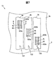
- FIG. 7 is a plan view showing a configuration example of the current detection device 13 according to the third embodiment of the present invention.
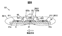
- FIG. 8 is a cross-sectional view taken along the line BB of FIG. 7, and includes a GMR element 41 orthogonal to the direction in which the currents I 1 , I 2 , and I 3 flow, as in the first and second embodiments. A cross section is shown.
- the direction of the magnetic field generated by the currents I 1 , I 2 , and I 3 and the detection direction of the magnetic field of the GMR element 41 are the same as those in the first and second embodiments.
- the current detection device 13 is similar to the current detection devices 11 and 12 according to the first and second embodiments, and the conductive member 6a and the GMR sensor 4a form a first current.
- the detection unit 131 the conductive member 6b and the GMR sensor 4b make a set
- the second current detection unit 132 the conductive member 6c and the GMR sensor 4c make a set
- the third current detection unit 133 respectively. It is composed.
- the GMR sensors 4a, 4b, and 4c are shifted from each other along the direction in which the currents I 1 , I 2 , and I 3 flow, and the accommodating portion 60 that accommodates the GMR sensors 4a, 4b, and 4c
- the conductive members 6a, 6b, and 6c are formed so as to be shifted from each other along the flow direction of 1 , I 2 , and I 3 .
- the first current detection unit 131 will be described as an example.
- the conductive member 6a has a pair of first conductive portions (left side) arranged in parallel with the GMR sensor 4a along the detection direction of the GMR element 41 on both sides of the GMR sensor 4a in the detection direction of the GMR element 41 in the cross section orthogonal to the current direction.
- Each of the part 611 and the right first conductive part 612 includes a parallel region 61 a parallel to the GMR element 41 along the detection direction of the GMR element 41.
- through holes 620a and 620b are formed in a portion aligned in a direction orthogonal to the detection direction of the GMR sensor 4a and the GMR element 41 in the cross section orthogonal to the current direction.
- the through holes 620a, 620b has been formed so as to extend along the direction of flow of the current I 1 in the accommodating portion 60 is not limited thereto, and the GMR sensor 4a in the least current direction orthogonal section It is only necessary that a through hole is formed in a portion aligned in a direction orthogonal to the detection direction of the GMR element 41.
- the number of through holes is not limited to two, and the number is not particularly limited.
- the second conductive portion 62 disposed on one side of the GMR sensor 4 a in the direction orthogonal to the detection direction of the GMR element 41 in the cross section perpendicular to the current direction of the conductive member 6 a detects the GMR element 41.
- the width in the direction parallel to the direction is formed smaller than the width in the direction parallel to the detection direction of the GMR element 41 in the GMR sensor 4a by forming the through holes 620a and 620b.
- the through holes 620 a and 620 b are provided with the second conductive portion 62 sandwiched in a direction parallel to the detection direction of the GMR element 41, and at least a part of the second conductive portion 62 is orthogonal to the detection direction of the GMR element 41. It is aligned with the GMR element 41 in the direction.
- the current I 1 is the first left conductive portion 611, the right first conductive portion 612, the second conductive portion 62, the first connecting portion 631,
- the two connected portions 632 flow in a distributed manner.
- the magnetic field B622 generated by the current I 1 flowing through the central portion of the second conductive portion 62 has the direction of the position where the GMR element 41 is disposed along the detection direction of the GMR element 41. It is detected by the sensor 4a.
- a magnetic field is also generated by the current I 1 flowing through the first connecting portion 231 and the second connecting portion 232, but for these magnetic fields, the intensity of the magnetic field of the component in the direction along the detection direction of the GMR element 41 is low. It is detected by the GMR sensor 4a.
- the intensity of the magnetic field detected by the GMR sensor 4a is the intensity of the magnetic field generated mainly by the current I 1 flowing through the second conductive portion 62 out of the magnetic field generated by the current I 1 flowing through the conductive member 6a.
- the conductive member 6a has a through-hole 620a, 620b formed in a portion aligned in a direction orthogonal to the detection direction of the GMR sensor 4a and the GMR element 41 in the cross section perpendicular to the current direction, whereby the current I 1 flowing through the second conductive portion 62 is formed. Therefore, the magnetic field generated by the current I 1 becomes smaller, and the magnetic field detected by the GMR sensor 4a can be further reduced.
- the through holes 620 a and 620 b are provided with the second conductive portion 62 sandwiched in a direction parallel to the detection direction of the GMR element 41, and at least a part of the second conductive portion 62 is orthogonal to the detection direction of the GMR element 41. Therefore, the GMR sensor 4a can detect the magnetic field with high accuracy.
- the GMR elements 41 of the GMR sensor 4a disposed corresponding to the conductive member 6a are disposed. There is no portion corresponding to the second conductive portion 62 in the direction along the detection direction.
- Conductive members (2a, 2b, 2c / 5a, 5b, 5c / 6a, 6b, 6c) through which currents to be detected (I 1 , I 2 , I 3 ) flow, and a magnetosensitive part (GMR element 41) And a detection sensor (GMR sensors 4a, 4b, 4c) for detecting the intensity of the magnetic field in a predetermined detection direction, and the conductive members (2a, 2b, 2c / 5a, 5b, 5c / 6a, 6b, 6c)
- a current detection device (11, 12, 13) in which a part of currents (I 1 , I 2 , I 3 ) flows in parallel regions (21a, 51a, 61a) parallel to the GMR element (41) along the detection direction.
- Conductive members (2a, 2b, 2c / 5a, 5b, 5c / 6a, 6b, 6c) have the GMR element (41) orthogonal to the direction in which the currents (I 1 , I 2 , I 3 ) flow.
- a first conductive part (211, 212/51/611, 612) arranged side by side with the GMR sensor (4 a, 4 b, 4 c) along the detection direction in the included cross section, and orthogonal to the detection direction in the current direction orthogonal cross section
- a second conductive part (22/52/62) disposed on one side of the GMR sensors (4a, 4b, 4c) in the direction of the first conductive part (211/212/51/611, 612) Includes the parallel region (21a, 51a, 61a), the current detection device (11, 12, 13) according to [1].
- the conductive members (2a, 2b, 2c / 5a, 5b, 5c / 6a, 6b, 6c) are composed of a first conductive part (211, 212/51/611, 612) and a second conductive part (22/52). / 62), the current detection device (11, 12, 13) according to any one of [2] to [4], which is integrally formed by bending a single metal plate.
- the second conductive portion (52/62) is formed such that the width in the direction parallel to the detection direction is smaller than the width in the direction parallel to the detection direction in the GMR sensors (4a, 4b, 4c).
- the current detection device (12, 13) according to any one of [2] to [5].
- through holes (620a, 620b) are formed in portions aligned with the GMR sensors (4a, 4b, 4c) and the direction orthogonal to the detection direction in the cross section orthogonal to the current direction.
- the current detection device (13) according to [6].
- the through holes (620a, 620b) are provided across the second conductive portion (62) in a direction parallel to the detection direction, and at least a part of the second conductive portion (62) is in the detection direction.
- the detection sensor according to any one of [1] to [8], wherein the detection sensor is a GMR sensor (4a, 4b, 4c) having a GMR element (41) having a giant magnetoresistive effect as a magnetosensitive portion.
- Current detectors (11, 12, 13).
- a plurality of sets of conductive members (6a, 6b, 6c) and GMR sensors (4a, 4b, 4c) are provided, and the plurality of conductive members (6a, 6b, 6c) include currents (I 1 , I 2 , I 3 ) are arranged so that the flowing directions thereof are parallel to each other, and the plurality of GMR sensors (4a, 4b, 4c) are arranged so as to be shifted from each other along the flowing direction of the currents (I 1 , I 2 , I 3 ).
- the current detection device (13) according to any one of [1] to [9].
- a plurality of sets of conductive members (2a, 2b, 2c / 5a, 5b, 5c / 6a, 6b, 6c) and GMR sensors (4a, 4b, 4c) are mounted on one side of the circuit board (3).
- the present invention can be appropriately modified and implemented without departing from the spirit of the present invention.
- the conductive member is formed by bending a thin metal plate.
- the present invention is not limited to this, and the material and shape can be changed according to the application of the current detection device. .
- the GMR sensors 4a, 4b, and 4c are mounted on the circuit board 3.
- the present invention is not limited to this.
- the GMR sensors 4a, 4b, and 4c may be directly connected to an external device via a connection cable.
- the specifications can be changed as appropriate according to the application.
- GMR sensors 4a, 4b, but 4c case has been described which is arranged offset in the direction of current flow I 1, I 2, I 3, the third embodiment
- the present invention can be applied to the first and second embodiments.
Landscapes
- Physics & Mathematics (AREA)
- General Physics & Mathematics (AREA)
- Measuring Instrument Details And Bridges, And Automatic Balancing Devices (AREA)
Abstract
大型化を抑制しながらも、電流の検出範囲を広くすることが可能な電流検出装置を提供する。 電流検出装置11は、検出対象の電流I1,I2,I3を流す導電部材2a,2b,2cと、感磁部を構成するGMR素子41における所定の検出方向の磁界の強度を検出するGMRセンサ4a,4b,4cとを備え、導電部材2a,2b,2cは、検出方向に沿ってGMR素子41に並列する並列領域21aに電流I1,I2,I3の一部が流れる。
Description
本発明は、磁界の強さを検出することによって導電部材に流れる電流を検出する電流検出装置に関する。
従来、電流検出装置として、例えば三相モータとインバータとの間における複数の電流路に流れる電流を、各電流路の近傍に設けられた電流検出センサを用いて検出するものが知られている(例えば、特許文献1参照。)。
特許文献1に記載の電流検出装置は、平板状の複数の電流路と、複数の電流路に流れる電流を検出する複数の電流検出センサとを備えている。電流検出センサは、電流路を流れる電流によって発生する磁界の強さを検出するMR素子等の磁束検出器、及び磁束検出器で検出された磁界の強さに基づいて電流路に流れる電流の電流値を検出する電流検出センサ本体を有している。
磁束検出器は、電流検出センサ本体を介して電流路の短手方向の中央付近に配置されている。また、磁束検出器は、磁界を検出することができる磁界検出方向が一方向に限られ、当該磁界検出方向は、電流の流れる方向に直交する方向、かつ電流路の短手方向に平行な方向である。
特許文献1に記載の電流検出装置では、電流路に流れる電流によって発生する磁界の強度が磁束検出器の感度に対して過大である場合には、電流路に流れる電流を正確に検出することができないため、電流の検出範囲が制限されてしまう。この対策として、例えば電流路と磁界検出器との間の距離を拡げることが考えられるが、この場合には電流検出装置が大型化してしまう。
そこで、本発明は、大型化を抑制しながらも、電流の検出範囲を広くすることが可能な電流検出装置を提供することを目的とする。
本発明は、上記課題を解決することを目的として、検出対象の電流を流す導電部材と、感磁部における所定の検出方向の磁界の強度を検出する検出センサとを備え、前記導電部材は、前記検出方向に沿って前記感磁部に並列する並列領域に前記電流の一部が流れる電流検出装置を提供する。
本発明に係る電流検出装置によれば、大型化を抑制しながらも、電流の検出範囲を広くすることが可能である。
[第1の実施の形態]
本発明の第1の実施の形態に係る電流検出装置について、図1乃至図3を参照して説明する。この電流検出装置は、例えば車両の駆動源としての三相モータのU相、V相、W相の各相に流れる電流を検出するために用いられる。
本発明の第1の実施の形態に係る電流検出装置について、図1乃至図3を参照して説明する。この電流検出装置は、例えば車両の駆動源としての三相モータのU相、V相、W相の各相に流れる電流を検出するために用いられる。
(電流検出装置11の構成)
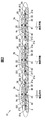
図1は、本発明の第1の実施の形態に係る電流検出装置11の一構成例を示す斜視図である。図2は、図1のA-A線断面図であり、具体的には、電流I1,I2,I3の流れる方向に直交してGMR素子41を含む断面を示している。
図1は、本発明の第1の実施の形態に係る電流検出装置11の一構成例を示す斜視図である。図2は、図1のA-A線断面図であり、具体的には、電流I1,I2,I3の流れる方向に直交してGMR素子41を含む断面を示している。
電流検出装置11は、検出対象の電流I1,I2,I3を流す導電部材2a,2b,2cと、感磁部における所定の検出方向の磁界の強度を検出する検出センサとしてのGMRセンサ4a,4b,4cと、GMRセンサ4a,4b,4cが実装された回路基板3とを備えている。本実施の形態では、感磁部は、巨大磁気抵抗効果を有する巨大磁気抵抗素子(GMR素子41)で構成されている。
ここで、巨大磁気抵抗効果(GMR;Giant Magneto Resistive effect)とは、小さな磁界の変化に対して大きな電気抵抗の変化を得ることができるものである。より具体的には、例えばホールIC等の磁気抵抗効果は、電気抵抗の変化率が数パーセント程度であるのに対し、この巨大磁気抵抗効果を用いた巨大磁気抵抗素子(GMR素子)は、電気抵抗の変化率が数十パーセント程度と大きい。GMR素子41は、例えばコバルト(Co)等の強磁性体の薄膜、及び例えば銅(Cu)等の非磁性体の薄膜を積層してなる。このGMR素子41を用いたGMRセンサ4a,4b,4cは、小さな電流に対しても高精度に電流を検出することが可能である。
図2に示すように、電流検出装置11には、導電部材2aに対してGMRセンサ4aが、導電部材2bに対してGMRセンサ4bが、導電部材2cに対してGMRセンサ4cが、それぞれ配置されている。以下、導電部材2aとGMRセンサ4aとの組を第1の電流検出ユニット111、導電部材2bとGMRセンサ4bとの組を第2の電流検出ユニット112、及び導電部材2cとGMRセンサ4cとの組を第3の電流検出ユニット113とする。
第1~第3の電流検出ユニット111~113は、回路基板3における一側の実装面3a上に並んで配置され、導電部材2a,2b,2cは、図1に示すように、電流I1,I2,I3の流れる方向が互いに平行となるように配置されている。回路基板3は、例えばポリ塩化ビフェニル(PCB)やガラスエポキシ等からなる。
(GMRセンサ4a,4b,4cの構成)
GMRセンサ4a,4b,4cはそれぞれ、センサ本体40と、GMR素子41と、回路基板3に例えば半田付け等により接続される複数の端子42(図2では、GMRセンサ4a,4b,4cそれぞれについて2つのみ示す)とを有している。
GMRセンサ4a,4b,4cはそれぞれ、センサ本体40と、GMR素子41と、回路基板3に例えば半田付け等により接続される複数の端子42(図2では、GMRセンサ4a,4b,4cそれぞれについて2つのみ示す)とを有している。
GMR素子41は、例えば一辺が10μmの正方形状であり、厚みは数μm程度である。本実施の形態では、図2に示すように、GMR素子41は、センサ本体40の中央部に位置し、磁界の検出方向が、回路基板3の実装面3aに平行かつ電流I1,I2,I3の流れる方向に対して垂直な方向である。なお、本実施の形態では、GMRセンサ4a,4b,4cそれぞれにおけるGMR素子41の磁界の検出方向は同一である。
(導電部材2a,2b,2cの構成)
導電部材2a,2b,2cは、その構成がすべて同一であるため、第1の電流検出ユニット111の導電部材2aを例にとって以下により詳細に説明する。
導電部材2a,2b,2cは、その構成がすべて同一であるため、第1の電流検出ユニット111の導電部材2aを例にとって以下により詳細に説明する。
図2に示すように、導電部材2aは、厚みが1.5mm程度の金属板を屈曲してなり、電流I1の流れる方向に延びている。また、導電部材2aは、電流I1の流れる方向に直交する幅方向の寸法が15mm程度であり、この幅方向の中央部にGMRセンサ4aが収容される収容部20を有している。
導電部材2aは、GMR素子41の検出方向に沿ってGMR素子41に並列する並列領域21aに電流I1の一部が流れている。なお、図2において、並列領域21aを二点鎖線で示す。この並列領域21aは、そこに流れる電流により発生する磁界の向きがGMR素子41の配置位置においてGMR素子41の磁界の検出方向に直交し、その磁界の強度がGMRセンサ4aによって検出されない領域である。
また、導電部材2aは、電流I1の流れる方向に直交してGMR素子41を含む断面においてGMR素子41の検出方向に沿ってGMRセンサ4aと並んで配置された一対の第1導電部211,212と、当該断面においてGMR素子41の検出方向に直交する方向におけるGMRセンサ4aの一側に配置された第2導電部22とを有し、第1導電部211,212に並列領域21aが含まれている。本実施の形態では、一対の第1導電部211,212及び第2導電部22は、回路基板3の実装面3aに対して平行である。
以下の説明において、「電流I1,I2,I3の流れる方向に直交してGMR素子41を含む断面」を単に「電流方向直交断面」とする。
一対の第1導電部211,212は、GMR素子41の検出方向におけるGMRセンサ4aの両側にそれぞれ配置されている。図2では、一方の第1導電部211がGMRセンサ4aの左側に、他方の第1導電部212がGMRセンサ4aの右側に、それぞれ配置されている。以下の説明において、便宜上、一方の第1導電部211を左側第1導電部211、他方の第1導電部212を右側第1導電部212とする。
第2導電部22は、GMR素子41の検出方向に直交する方向において、回路基板3との間にGMRセンサ4aが位置するように、GMRセンサ4aの一側に配置されている。
本実施の形態では、第2導電部22は、GMR素子41の検出方向に平行な方向の幅が、GMRセンサ4aにおけるGMR素子41の検出方向に平行な方向の幅と同一であり、かつ左側第1導電部211、右側第1導電部212、及び第2導電部22は、GMR素子41の検出方向に平行な方向の幅が、すべて同一に設定されているが、これに限らず、電流検出装置11の用途に応じて設定することが可能である。
導電部材2aは、電流方向直交断面において、左側第1導電部211と第2導電部22との間を連結する第1連結部231、及び右側第1導電部212と第2導電部22との間を連結する第2連結部232をさらに有している。
第1連結部231及び第2連結部232は、左側第1導電部211、右側第1導電部212、及び第2導電部22に対して傾斜するように形成されている。なお、これに限らず、例えば第1連結部231は、左側第1導電部211及び第2導電部22に対して直交するように形成されていてもよい。第2連結部232についても同様である。
導電部材2aは、左側第1導電部211、右側第1導電部212、第2導電部22、第1連結部231、及び第2連結部232が、1枚の金属板を屈曲することにより一体に形成されている。なお、これに限らず、導電部材2aは、例えば第1連結部231を有さず、左側第1導電部211と第2導電部22とが離間していてもよいし、第2連結部232を有さず、右側第1導電部212と第2導電部22とが離間していてもよい。
本実施の形態では、第2導電部22、第1連結部231、及び第2連結部232が、収容部20の一部を構成している。
(発生する磁界及び検出される磁界について)
次に、電流I1,I2,I3によって発生する磁界、及びGMRセンサ4a,4b,4cにて検出される磁界について説明する。
次に、電流I1,I2,I3によって発生する磁界、及びGMRセンサ4a,4b,4cにて検出される磁界について説明する。
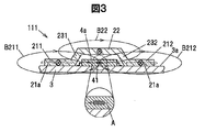
図3は、図2における第1の電流検出ユニット111を示す断面図である。なお、電流I1,I2,I3によって発生する磁界、及び各GMRセンサ4a,4b,4cにて検出される磁界についても、第1~第3の電流検出ユニット111~113においてすべて同一であるため、第1の電流検出ユニット111を例にとって以下説明する。
電流I1は、導電部材2aの電流方向直交断面において、左側第1導電部211、右側第1導電部212、第2導電部22、第1連結部231、及び第2連結部232のそれぞれに分散して流れる。
図3において、電流I1によって発生する磁界の向きは時計回りである。また、本実施の形態では、GMR素子41の磁界の検出方向は、右側第1導電部212から左側第1導電部211に向かう方向(図3の矢印A)である。
左側第1導電部211の中心部に流れる電流I1によって発生する磁界B211は、GMR素子41の配置位置での方向が、第2導電部22側から回路基板3側へ向かっており、GMR素子41の検出方向に対して直交している。同様にして、右側第1導電部212の中心部に流れる電流I1によって発生する磁界B212は、GMR素子41の配置位置での方向が、回路基板3側から第2導電部22側へ向かっており、GMR素子41の検出方向に直交している。
したがって、GMR素子41の配置位置での磁界B211の方向及び磁界B212の方向は、GMR素子41の検出方向に沿わないため、磁界B211の強度及び磁界B212の強度はGMRセンサ4aにて検出されない。
第2導電部22の中心部に流れる電流I1によって発生する磁界B22は、GMR素子41の配置位置での方向が、右側第1導電部212側から左側第1導電部211側へ向かっており、GMR素子41の検出方向に沿う。したがって、磁界B22の強度は、GMRセンサ4aにて検出される。
なお、第1及び第2連結部231,232に流れる電流I1によっても磁界は発生するが、これらの磁界については、GMR素子41の検出方向に沿う方向の成分の磁界の強度がGMRセンサ4aにて検出される。
以上より、GMRセンサ4aで検出される磁界の強度は、導電部材2aを流れる電流I1によって発生する磁界のうち、主に第2導電部22を流れる電流I1によって発生する磁界の強度となる。
(第1の実施の形態の作用及び効果)
以上説明した第1の実施の形態によれば、以下のような作用及び効果が得られる。
以上説明した第1の実施の形態によれば、以下のような作用及び効果が得られる。
(1)導電部材2a,2b,2cは、GMR素子41の検出方向にGMR素子41と並列する並列領域21aに電流I1,I2,I3の一部がそれぞれ流れることによって、GMRセンサ4a,4b,4cで検出される磁界が低減される。したがって、導電部材2a,2b,2cに大電流が流れてGMRセンサ4a,4b,4cの周囲においてGMR素子41の感度に対して過大な磁界が発生した場合でも、導電部材2a,2b,2cとGMRセンサ4a,4b,4cとの間の距離を拡げる必要がなく電流検出装置11の大型化を抑制することが可能であり、正確に検出可能な磁界の強度の範囲が大きくなる。
(2)導電部材2a,2b,2cは、第1導電部211,212及び第2導電部22が、1枚の金属板を屈曲することにより一体に形成されているため、第1導電部211,212及び第2導電部22を形成するための金属部材をそれぞれ用意したり、これらの金属部材を組み合わせる必要がなく、作業性の向上及びコストの削減を図ることが可能である。
(3)電流検出装置11は、導電部材2a,2b,2cを流れる電流I1,I2,I3によって発生する磁界の強度を検出する検出センサとして、GMR素子41を有するGMRセンサ4a,4b,4cを用いているため、例えばホールIC等のセンサと比較して感度がよく、発生する磁界の強度をダイナミックレンジ(例えば0.002mT~2.000mT)で精度よく検出することが可能である。
(4)第1~第3の電流検出ユニット111~113は、回路基板3における一側の実装面3a上に並んで配置されているため、配線の取り回しや、第1~第3の電流検出ユニット111~113を回路基板3に取り付ける作業等が容易になる。
(5)導電部材2a,2b,2cは、電流I1,I2,I3の流れる方向に直交してGMR素子41を含む断面においてGMR素子41の検出方向におけるGMRセンサ4a,4b,4cの両側にGMR素子41の検出方向に沿ってGMRセンサ4a,4b,4cと並んで配置された左側第1導電部211及び右側第1導電部212と、当該電流方向直交断面においてGMR素子41の検出方向に直交する方向におけるGMRセンサ4a,4b,4cの一側に配置された第2導電部22とを有し、左側第1導電部211及び右側第1導電部212に並列領域21aが含まれているため、導電部材2a,2b,2cを流れる電流I1,I2,I3が左側第1導電部211、右側第1導電部212、及び第2導電部22のそれぞれに主に分散される。これにより、GMRセンサ4a,4b,4cでそれぞれ検出される磁界をより低減することができる。
[第2の実施の形態]
次に、本発明の第2の実施の形態について、図4及び図5を参照して説明する。
次に、本発明の第2の実施の形態について、図4及び図5を参照して説明する。
図4及び図5において、第1の実施の形態について説明したものと実質的に同一の機能を有する構成要素については、共通する符号を付してその重複した説明を省略する。
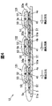
図4は、本発明の第2の実施の形態に係る電流検出装置12の一構成例を示す断面図であり、第1の実施の形態と同様に、電流I1,I2,I3の流れる方向に直交してGMR素子41を含む断面を示している。なお、図4において、電流I1,I2,I3によって発生する磁界の向き、及びGMR素子41の磁界の検出方向は、第1の実施の形態と同様である。
第2の実施の形態に係る電流検出装置12は、導電部材5a,5b,5cの構成が第1の実施の形態に係る導電部材2a,2b,2cの構成と異なり、それ以外の構成については第1の実施の形態に係る電流検出装置11の構成と同様である。
電流検出装置12は、第1の実施の形態と同様に、導電部材5aとGMRセンサ4aとが組をなして第1の電流検出ユニット121を、導電部材5bとGMRセンサ4bとが組をなして第2の電流検出ユニット122を、導電部材5cとGMRセンサ4cとが組をなして第3の電流検出ユニット123を、それぞれ構成している。
本実施の形態においても、第1の実施の形態と同様に、第1~第3の電流検出ユニット121~123の構成はすべて同一であるため、第1の電流検出ユニット121を例にとって以下説明する。
導電部材5aは、電流方向直交断面において、GMR素子41の検出方向におけるGMRセンサ4aの片側にGMR素子41の検出方向に沿ってGMRセンサ4aと並んで配置された第1導電部51と、GMR素子41の検出方向に直交する方向におけるGMRセンサ4aの一側に配置された第2導電部52とを有し、第1導電部51には、GMR素子41の検出方向に沿ってGMR素子41に並列する並列領域51aが含まれている。
すなわち、第1の実施の形態に係る導電部材2aは、左側第1導電部211及び右側第1導電部212が、GMR素子41の検出方向におけるGMRセンサ4aの両側にそれぞれ配置されていたのに対し、本実施の形態に係る導電部材5aは、第1導電部51が、GMR素子41の検出方向におけるGMRセンサ4aの片側に配置されている。すなわち、第1導電部51は、GMR素子41の検出方向におけるGMRセンサ4aの一側に配置され、GMR素子41の検出方向におけるGMRセンサ4aの他側には第1導電部が配置されていない。図4では、第1導電部51は、GMR素子41の検出方向において第2導電部52の左側に配置されている。
第2導電部52は、第1の実施の形態と同様に、GMR素子41の検出方向に直交する方向において、回路基板3との間にGMRセンサ4aが位置するように、GMRセンサ4aの一側に配置され、GMR素子41の検出方向に平行な方向の幅が、GMRセンサ4aにおけるGMR素子41の検出方向に平行な方向の幅と同一である。
導電部材5aは、電流方向直交断面において、第1導電部51と第2導電部52との間に、第1導電部51及び第2導電部52に対して傾斜した連結部53をさらに有している。一方、導電部材5aにおいて、GMR素子41の検出方向における連結部53とは反対側には、開口50aが形成されている。
導電部材5aは、第1の実施の形態と同様に、第1導電部51、第2導電部52、及び連結部53が、1枚の金属板を屈曲することにより一体に形成されている。本実施の形態では、第2導電部52及び連結部53が、GMRセンサ4aが収容される収容部50の一部となっている。
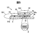
図5は、図4における第1の電流検出ユニット121を示す断面図である。図5において、GMR素子41の磁界の検出方向を矢印Aで示す。
電流I1は、導電部材5aにおける電流方向直交断面において、第1導電部51、第2導電部52、及び連結部53のそれぞれに分散して流れる。
第1導電部51の中心部に流れる電流I1によって発生する磁界B51は、GMR素子41の配置位置での方向が、第2導電部52側から回路基板3側へ向かっており、GMR素子41の検出方向に対して直交している。したがって、GMR素子41の配置位置での磁界B51の方向は、GMR素子41の検出方向に沿わないため、磁界B51の強度はGMRセンサ4aにて検出されない。
第2導電部52の中心部に流れる電流I1によって発生する磁界B52は、GMR素子41の配置位置での方向が、開口50a側から第1導電部51側へ向かっており、GMR素子41の検出方向に沿う。したがって、磁界B52の強度は、GMRセンサ4aにて検出される。
なお、連結部53に流れる電流I1によっても磁界は発生するが、この磁界については、GMR素子41の検出方向に沿う方向の成分の磁界の強度がGMRセンサ4aにて検出される。
以上より、GMRセンサ4aで検出される磁界の強度は、導電部材5aを流れる電流I1によって発生する磁界のうち、主に第2導電部52を流れる電流I1によって発生する磁界の強度となる。
(第2の実施の形態の作用及び効果)
以上説明した第2の実施の形態によっても、第1の実施の形態の(1)~(4)の作用及び効果と同様の作用及び効果が得られる。
以上説明した第2の実施の形態によっても、第1の実施の形態の(1)~(4)の作用及び効果と同様の作用及び効果が得られる。
(第2の実施の形態の変形例)
また、第2の実施の形態に係る電流検出装置12は、以下のように変形して実施することが可能である。
また、第2の実施の形態に係る電流検出装置12は、以下のように変形して実施することが可能である。
図6は、第2の実施の形態の変形例に係る第1の電流検出ユニット121を示す断面図である。
本変形例では、第2導電部520におけるGMR素子41の検出方向に平行な方向の幅が、GMRセンサ4aにおけるGMR素子41の検出方向に平行な方向の幅よりも小さく形成されている。したがって、導電部材5a側からGMR素子41の検出方向に直交する方向に第1の電流検出ニット121を見た場合、GMRセンサ4aの一部が収容部50から露出している。
本変形例によれば、第2導電部520に流れる電流I1が少なくなるため、電流I1によって発生する磁界が小さくなりGMRセンサ4aで検出される磁界をより低減することができる。
[第3の実施の形態]
次に、本発明の第3の実施の形態について、図7及び図8を参照して説明する。
次に、本発明の第3の実施の形態について、図7及び図8を参照して説明する。
図7及び図8において、第1の実施の形態について説明したものと実質的に同一の機能を有する構成要素については、共通する符号を付してその重複した説明を省略する。
図7は、本発明の第3の実施の形態に係る電流検出装置13の一構成例を示す平面図である。図8は、図7のB-B線断面図であり、第1及び第2の実施の形態と同様に、電流I1,I2,I3の流れる方向に直交してGMR素子41を含む断面を示している。なお、図8において、電流I1,I2,I3によって発生する磁界の向き、及びGMR素子41の磁界の検出方向は、第1及び第2の実施の形態と同様である。
本実施の形態に係る電流検出装置13は、第1及び第2の実施の形態に係る電流検出装置11,12と同様に、導電部材6aとGMRセンサ4aとが組をなして第1の電流検出ユニット131を、導電部材6bとGMRセンサ4bとが組をなして第2の電流検出ユニット132を、導電部材6cとGMRセンサ4cとが組をなして第3の電流検出ユニット133を、それぞれ構成している。
電流検出装置13は、GMRセンサ4a,4b,4cが、電流I1,I2,I3の流れる方向に沿って互いにずれ、GMRセンサ4a,4b,4cを収容する収容部60は、電流I1,I2,I3の流れる方向に沿って互いにずれて導電部材6a,6b,6cにそれぞれ形成されている。
本実施の形態においても、第1及び第2の実施の形態と同様に、第1の電流検出ユニット131を例にとって説明する。
導電部材6aは、電流方向直交断面において、GMR素子41の検出方向におけるGMRセンサ4aの両側にGMR素子41の検出方向に沿ってGMRセンサ4aと並んで配置された一対の第1導電部(左側第1導電部611及び右側第1導電部612)と、GMR素子41の検出方向に直交する方向におけるGMRセンサ4aの一側に配置された第2導電部62とを有し、左側第1導電部611及び右側第1導電部612には、GMR素子41の検出方向に沿ってGMR素子41に並列する並列領域61aがそれぞれ含まれている。
導電部材6aは、電流方向直交断面においてGMRセンサ4aとGMR素子41の検出方向に直交する方向に並ぶ部位に貫通孔620a,620bが形成されている。本実施の形態では、貫通孔620a,620bは、収容部60において電流I1の流れる方向に沿って延びるように形成されているが、これに限らず、少なくとも電流方向直交断面においてGMRセンサ4aとGMR素子41の検出方向に直交する方向に並ぶ部位に貫通孔が形成されていればよい。また、貫通孔の数は2つに限る必要はなく、その数について特に制限はない。
図7に示すように、導電部材6a側からGMR素子41の検出方向に直交する方向に第1の電流検出ユニット131を見た場合、GMRセンサ4aの一部が貫通孔620a,620bを介して収容部60から露出している。
図8に示すように、導電部材6aの電流方向直交断面において、GMR素子41の検出方向に直交する方向におけるGMRセンサ4aの一側に配置された第2導電部62は、GMR素子41の検出方向に平行な方向の幅が、貫通孔620a,620bが形成されることによって、GMRセンサ4aにおけるGMR素子41の検出方向に平行な方向の幅よりも小さく形成されている。
貫通孔620a,620bは、GMR素子41の検出方向に平行な方向に第2導電部62を挟んで設けられ、第2導電部62は、その少なくとも一部がGMR素子41の検出方向に直交する方向にGMR素子41と並んでいる。
図8に示すように、電流I1は、導電部材6aの電流方向直交断面において、左側第1導電部611、右側第1導電部612、第2導電部62、第1連結部631、及び第2連結部632のそれぞれに分散して流れる。
第1の実施の形態と同様に、左側第1導電部611の中心部及び右側第1導電部612の中心部に流れる電流I1によって発生する磁界B611及び磁界B612は、GMR素子41の配置位置での方向が、GMR素子41の検出方向に直交するため、GMR素子41の検出方向沿わず磁界B611の強度及び磁界B612の強度はGMRセンサ4aにて検出されない。
一方、第2導電部62の中心部に流れる電流I1によって発生する磁界B622は、GMR素子41の配置位置での方向が、GMR素子41の検出方向に沿うため、磁界B622の強度は、GMRセンサ4aにて検出される。
なお、第1の連結部231、及び第2連結部232に流れる電流I1によっても磁界は発生するが、これらの磁界については、GMR素子41の検出方向に沿う方向の成分の磁界の強度がGMRセンサ4aにて検出される。
以上より、GMRセンサ4aで検出される磁界の強度は、導電部材6aを流れる電流I1によって発生する磁界のうち、主に第2導電部62を流れる電流I1によって発生する磁界の強度となる。
(第3の実施の形態の作用及び効果)
以上説明した第2の実施の形態によっても、第1の実施の形態の(1)~(5)の作用及び効果と同様の作用及び効果の他に、以下の作用及び効果が得られる。
以上説明した第2の実施の形態によっても、第1の実施の形態の(1)~(5)の作用及び効果と同様の作用及び効果の他に、以下の作用及び効果が得られる。
導電部材6aは、電流方向直交断面においてGMRセンサ4aとGMR素子41の検出方向に直交する方向に並ぶ部位に貫通孔620a,620bが形成されることにより、第2導電部62に流れる電流I1がより少なくなるため、電流I1によって発生する磁界がより小さくなりGMRセンサ4aで検出される磁界をさらに低減することができる。
貫通孔620a,620bは、GMR素子41の検出方向に平行な方向に第2導電部62を挟んで設けられ、第2導電部62は、その少なくとも一部が、GMR素子41の検出方向に直交する方向にGMR素子41と並んでいるため、GMRセンサ4aにおいて精度よく磁界を検出することが可能となる。
GMRセンサ4a,4b,4cは、電流I1,I2,I3の流れる方向に沿って互いにずれて配置されているため、導電部材6aに対応して配置されたGMRセンサ4aのGMR素子41の検出方向に沿った方向に第2導電部62に該当する部分が存在しない。導電部材6bに対応して配置されたGMRセンサ4b及び導電部材6cに対応して配置されたGMRセンサ4cに関しても同様である。したがって、GMRセンサ4a,4b,4cの配置位置において導電部材6a,6b,6c間の磁界の干渉を抑制することができる。
(実施の形態のまとめ)
次に、以上説明した実施の形態から把握される技術思想について、実施の形態における符号等を援用して記載する。ただし、以下の記載における各符号等は、特許請求の範囲における構成要素を実施の形態に具体的に示した部材等に限定するものではない。
次に、以上説明した実施の形態から把握される技術思想について、実施の形態における符号等を援用して記載する。ただし、以下の記載における各符号等は、特許請求の範囲における構成要素を実施の形態に具体的に示した部材等に限定するものではない。
[1]検出対象の電流(I1,I2,I3)を流す導電部材(2a,2b,2c/5a,5b,5c/6a,6b,6c)と、感磁部(GMR素子41)における所定の検出方向の磁界の強度を検出する検出センサ(GMRセンサ4a,4b,4c)とを備え、導電部材(2a,2b,2c/5a,5b,5c/6a,6b,6c)は、検出方向に沿ってGMR素子(41)に並列する並列領域(21a,51a,61a)に電流(I1,I2,I3)の一部が流れる電流検出装置(11,12,13)。
[2]導電部材(2a,2b,2c/5a,5b,5c/6a,6b,6c)は、電流(I1,I2,I3)の流れる方向に直交してGMR素子(41)を含む断面において検出方向に沿ってGMRセンサ(4a,4b,4c)と並んで配置された第1導電部(211,212/51/611,612)と、当該電流方向直交断面において検出方向に直交する方向におけるGMRセンサ(4a,4b,4c)の一側に配置された第2導電部(22/52/62)とを有し、第1導電部(211,212/51/611,612)に並列領域(21a,51a,61a)が含まれる、[1]に記載の電流検出装置(11,12,13)。
[3]第1導電部(51)は、検出方向におけるGMRセンサ(4a,4b,4c)の片側に配置された、[2]に記載の電流検出装置(12)。
[4]第1導電部(211,212/611,612)は、検出方向におけるGMRセンサ(4a,4b,4c)の両側にそれぞれ配置された、[2]に記載の電流検出装置(11,13)。
[5]導電部材(2a,2b,2c/5a,5b,5c/6a,6b,6c)は、第1導電部(211,212/51/611,612)及び第2導電部(22/52/62)が、1枚の金属板を屈曲することにより一体に形成されている、[2]乃至[4]の何れか1項に記載の電流検出装置(11,12,13)。
[6]第2導電部(52/62)は、検出方向に平行な方向の幅が、GMRセンサ(4a,4b,4c)における検出方向に平行な方向の幅よりも小さく形成されている、[2]乃至[5]の何れか1項に記載の電流検出装置(12,13)。
[7]導電部材(6a,6b,6c)は、当該電流方向直交断面においてGMRセンサ(4a,4b,4c)と検出方向に直交する方向に並ぶ部位に貫通孔(620a,620b)が形成された、[6]に記載の電流検出装置(13)。
[8]貫通孔(620a,620b)は、検出方向に平行な方向に第2導電部(62)を挟んで設けられ、第2導電部(62)は、その少なくとも一部が、検出方向に直交する方向にGMR素子41と並ぶ、[7]に記載の電流検出装置(13)。
[9]検出センサは、感磁部として巨大磁気抵抗効果を有するGMR素子(41)を有するGMRセンサ(4a,4b,4c)である、[1]乃至[8]の何れか1項に記載の電流検出装置(11,12,13)。
[10]導電部材(6a,6b,6c)及びGMRセンサ(4a,4b,4c)の組を複数組備え、複数の導電部材(6a,6b,6c)は、電流(I1,I2,I3)の流れる方向が互いに平行となるように配置され、複数のGMRセンサ(4a,4b,4c)は、電流(I1,I2,I3)の流れる方向に沿って互いにずれて配置されている、[1]乃至[9]の何れか1項に記載の電流検出装置(13)。
[11]複数組の導電部材(2a,2b,2c/5a,5b,5c/6a,6b,6c)及びGMRセンサ(4a,4b,4c)は、回路基板(3)における一側の実装面(3a)上に並んで配置されている、[10]に記載の電流検出装置(11,12,13)。
以上、本発明の実施の形態を説明したが、上記に記載した実施の形態は特許請求の範囲に係る発明を限定するものではない。また、実施の形態の中で説明した特徴の組合せの全てが発明の課題を解決するための手段に必須であるとは限らない点に留意すべきである。
本発明は、その趣旨を逸脱しない範囲で適宜変形して実施することが可能である。例えば、上記実施の形態では、導電部材は厚みの薄い金属板を屈曲して形成されていたが、これに限らず、電流検出装置の用途に応じて材料や形状を変更することが可能である。
また、上記実施の形態では、GMRセンサ4a,4b,4cは、回路基板3に実装されているが、これに限らず、例えば接続ケーブルを介して外部機器に直接接続する等、電流検出装置の用途に応じて適宜仕様を変更することが可能である。
また、上記第3の実施の形態において、GMRセンサ4a,4b,4cが電流I1,I2,I3の流れる方向にずれて配置されている場合について説明したが、第3の実施の形態に限らず、第1及び第2の実施の形態においても適用することが可能である。
2a,2b,2c,5a,5b,5c,6a,6b,6c…導電部材
3…回路基板
3a…実装面
4a,4b,4c…GMRセンサ(検出センサ)
11,12,13…電流検出装置
21a,51a,61a…並列領域
22,52,520,62…第2導電部
41…GMR素子(感磁部)
51,211,212,611,612…第1導電部
111~113,121~123,131~133…第1~第3の電流検出ユニット
620a,620b…貫通孔
3…回路基板
3a…実装面
4a,4b,4c…GMRセンサ(検出センサ)
11,12,13…電流検出装置
21a,51a,61a…並列領域
22,52,520,62…第2導電部
41…GMR素子(感磁部)
51,211,212,611,612…第1導電部
111~113,121~123,131~133…第1~第3の電流検出ユニット
620a,620b…貫通孔
Claims (11)
- 検出対象の電流を流す導電部材と、
感磁部における所定の検出方向の磁界の強度を検出する検出センサとを備え、
前記導電部材は、前記検出方向に沿って前記感磁部に並列する並列領域に前記電流の一部が流れる
電流検出装置。 - 前記導電部材は、前記電流の流れる方向に直交して前記感磁部を含む断面において前記検出方向に沿って前記検出センサと並んで配置された第1導電部と、前記断面において前記検出方向に直交する方向における前記検出センサの一側に配置された第2導電部とを有し、前記第1導電部に前記並列領域が含まれる、
請求項1に記載の電流検出装置。 - 前記第1導電部は、前記検出方向における前記検出センサの片側に配置された、
請求項2に記載の電流検出装置。 - 前記第1導電部は、前記検出方向における前記検出センサの両側にそれぞれ配置された、
請求項2に記載の電流検出装置。 - 前記導電部材は、前記第1導電部及び前記第2導電部が、1枚の金属板を屈曲することにより一体に形成されている、
請求項2乃至4の何れか1項に記載の電流検出装置。 - 前記第2導電部は、前記検出方向に平行な方向の幅が、前記検出センサにおける前記検出方向に平行な方向の幅よりも小さく形成されている、
請求項2乃至5の何れか1項に記載の電流検出装置。 - 前記導電部材は、前記断面において前記検出センサと前記検出方向に直交する方向に並ぶ部位に貫通孔が形成された、
請求項6に記載の電流検出装置。 - 前記貫通孔は、前記検出方向に平行な方向に前記第2導電部を挟んで設けられ、
前記第2導電部は、その少なくとも一部が、前記検出方向に直交する方向に前記感磁部と並ぶ、
請求項7に記載の電流検出装置。 - 前記検出センサは、前記感磁部として巨大磁気抵抗効果を有するGMR素子を有するGMRセンサである、
請求項1乃至8の何れか1項に記載の電流検出装置。 - 前記導電部材及び前記検出センサの組を複数組備え、
複数の前記導電部材は、前記電流の流れる方向が互いに平行となるように配置され、
複数の前記検出センサは、前記電流の流れる方向に沿って互いにずれて配置されている、
請求項1乃至9の何れか1項に記載の電流検出装置。 - 複数組の前記導電部材及び前記検出センサは、回路基板における一側の実装面上に並んで配置されている、
請求項10に記載の電流検出装置。
Priority Applications (1)
| Application Number | Priority Date | Filing Date | Title |
|---|---|---|---|
| PCT/JP2014/053900 WO2015125232A1 (ja) | 2014-02-19 | 2014-02-19 | 電流検出装置 |
Applications Claiming Priority (1)
| Application Number | Priority Date | Filing Date | Title |
|---|---|---|---|
| PCT/JP2014/053900 WO2015125232A1 (ja) | 2014-02-19 | 2014-02-19 | 電流検出装置 |
Publications (1)
| Publication Number | Publication Date |
|---|---|
| WO2015125232A1 true WO2015125232A1 (ja) | 2015-08-27 |
Family
ID=53877767
Family Applications (1)
| Application Number | Title | Priority Date | Filing Date |
|---|---|---|---|
| PCT/JP2014/053900 Ceased WO2015125232A1 (ja) | 2014-02-19 | 2014-02-19 | 電流検出装置 |
Country Status (1)
| Country | Link |
|---|---|
| WO (1) | WO2015125232A1 (ja) |
Citations (4)
| Publication number | Priority date | Publication date | Assignee | Title |
|---|---|---|---|---|
| JP2002202328A (ja) * | 2000-12-28 | 2002-07-19 | Japan System Engineering Kk | 磁界型電流センサ |
| JP2005031000A (ja) * | 2003-07-09 | 2005-02-03 | Asahi Kasei Electronics Co Ltd | 電流測定方法及び電流測定装置 |
| JP2005321206A (ja) * | 2004-05-06 | 2005-11-17 | Mitsubishi Electric Corp | 電流検出装置 |
| JP2011080970A (ja) * | 2009-10-02 | 2011-04-21 | Kohshin Electric Corp | 多相電流の検出装置 |
-
2014
- 2014-02-19 WO PCT/JP2014/053900 patent/WO2015125232A1/ja not_active Ceased
Patent Citations (4)
| Publication number | Priority date | Publication date | Assignee | Title |
|---|---|---|---|---|
| JP2002202328A (ja) * | 2000-12-28 | 2002-07-19 | Japan System Engineering Kk | 磁界型電流センサ |
| JP2005031000A (ja) * | 2003-07-09 | 2005-02-03 | Asahi Kasei Electronics Co Ltd | 電流測定方法及び電流測定装置 |
| JP2005321206A (ja) * | 2004-05-06 | 2005-11-17 | Mitsubishi Electric Corp | 電流検出装置 |
| JP2011080970A (ja) * | 2009-10-02 | 2011-04-21 | Kohshin Electric Corp | 多相電流の検出装置 |
Similar Documents
| Publication | Publication Date | Title |
|---|---|---|
| JP6651956B2 (ja) | 電流センサ | |
| CN107533089B (zh) | 电流传感器 | |
| US10605835B2 (en) | Current sensor | |
| JP6467696B2 (ja) | 電流測定装置 | |
| US10274523B2 (en) | Current sensor including a first current sensor and a second current sensor unit | |
| JPWO2018100778A1 (ja) | 電流センサ及び電流センサユニット | |
| JP2015210272A (ja) | ハイブリッド電流センサアセンブリ | |
| CN107430155A (zh) | 电流传感器 | |
| JP2018004314A (ja) | 電流センサ | |
| EP3106884B1 (en) | Current sensor | |
| US10267825B2 (en) | Current sensor including a housing surrounded by bent portions of primary conductors | |
| WO2018159229A1 (ja) | 電流検出装置 | |
| JP6827058B2 (ja) | 電流センサ | |
| JP2018096794A (ja) | 電流センサ | |
| JP2012026966A (ja) | 電流センサ | |
| JP6506604B2 (ja) | 磁気センサ | |
| WO2014123007A1 (ja) | 電流センサ | |
| US10502767B2 (en) | Electric current detection device and electric current detection method | |
| WO2015125232A1 (ja) | 電流検出装置 | |
| JP2013142604A (ja) | 電流センサ | |
| JP6413267B2 (ja) | 電流検出構造 | |
| US11150276B2 (en) | Current detection device | |
| WO2015125233A1 (ja) | 電流検出装置 | |
| WO2016080135A1 (ja) | 電流センサ | |
| JP2012215488A (ja) | 電流センサ |
Legal Events
| Date | Code | Title | Description |
|---|---|---|---|
| 121 | Ep: the epo has been informed by wipo that ep was designated in this application |
Ref document number: 14883173 Country of ref document: EP Kind code of ref document: A1 |
|
| NENP | Non-entry into the national phase |
Ref country code: DE |
|
| 122 | Ep: pct application non-entry in european phase |
Ref document number: 14883173 Country of ref document: EP Kind code of ref document: A1 |
|
| NENP | Non-entry into the national phase |
Ref country code: JP |