WO2015087828A1 - 水の電気分解システム - Google Patents
水の電気分解システム Download PDFInfo
- Publication number
- WO2015087828A1 WO2015087828A1 PCT/JP2014/082406 JP2014082406W WO2015087828A1 WO 2015087828 A1 WO2015087828 A1 WO 2015087828A1 JP 2014082406 W JP2014082406 W JP 2014082406W WO 2015087828 A1 WO2015087828 A1 WO 2015087828A1
- Authority
- WO
- WIPO (PCT)
- Prior art keywords
- photoelectric conversion
- electrode
- hydrogen
- oxygen
- gas
- Prior art date
- Legal status (The legal status is an assumption and is not a legal conclusion. Google has not performed a legal analysis and makes no representation as to the accuracy of the status listed.)
- Ceased
Links
Images

Classifications
-
- C—CHEMISTRY; METALLURGY
- C25—ELECTROLYTIC OR ELECTROPHORETIC PROCESSES; APPARATUS THEREFOR
- C25B—ELECTROLYTIC OR ELECTROPHORETIC PROCESSES FOR THE PRODUCTION OF COMPOUNDS OR NON-METALS; APPARATUS THEREFOR
- C25B1/00—Electrolytic production of inorganic compounds or non-metals
- C25B1/01—Products
- C25B1/02—Hydrogen or oxygen
- C25B1/04—Hydrogen or oxygen by electrolysis of water
-
- C—CHEMISTRY; METALLURGY
- C25—ELECTROLYTIC OR ELECTROPHORETIC PROCESSES; APPARATUS THEREFOR
- C25B—ELECTROLYTIC OR ELECTROPHORETIC PROCESSES FOR THE PRODUCTION OF COMPOUNDS OR NON-METALS; APPARATUS THEREFOR
- C25B1/00—Electrolytic production of inorganic compounds or non-metals
- C25B1/50—Processes
- C25B1/55—Photoelectrolysis
-
- C—CHEMISTRY; METALLURGY
- C25—ELECTROLYTIC OR ELECTROPHORETIC PROCESSES; APPARATUS THEREFOR
- C25B—ELECTROLYTIC OR ELECTROPHORETIC PROCESSES FOR THE PRODUCTION OF COMPOUNDS OR NON-METALS; APPARATUS THEREFOR
- C25B15/00—Operating or servicing cells
- C25B15/02—Process control or regulation
-
- C—CHEMISTRY; METALLURGY
- C25—ELECTROLYTIC OR ELECTROPHORETIC PROCESSES; APPARATUS THEREFOR
- C25B—ELECTROLYTIC OR ELECTROPHORETIC PROCESSES FOR THE PRODUCTION OF COMPOUNDS OR NON-METALS; APPARATUS THEREFOR
- C25B9/00—Cells or assemblies of cells; Constructional parts of cells; Assemblies of constructional parts, e.g. electrode-diaphragm assemblies; Process-related cell features
- C25B9/17—Cells comprising dimensionally-stable non-movable electrodes; Assemblies of constructional parts thereof
- C25B9/19—Cells comprising dimensionally-stable non-movable electrodes; Assemblies of constructional parts thereof with diaphragms
-
- H—ELECTRICITY
- H10—SEMICONDUCTOR DEVICES; ELECTRIC SOLID-STATE DEVICES NOT OTHERWISE PROVIDED FOR
- H10F—INORGANIC SEMICONDUCTOR DEVICES SENSITIVE TO INFRARED RADIATION, LIGHT, ELECTROMAGNETIC RADIATION OF SHORTER WAVELENGTH OR CORPUSCULAR RADIATION
- H10F10/00—Individual photovoltaic cells, e.g. solar cells
- H10F10/10—Individual photovoltaic cells, e.g. solar cells having potential barriers
- H10F10/16—Photovoltaic cells having only PN heterojunction potential barriers
- H10F10/167—Photovoltaic cells having only PN heterojunction potential barriers comprising Group I-III-VI materials, e.g. CdS/CuInSe2 [CIS] heterojunction photovoltaic cells
-
- H—ELECTRICITY
- H10—SEMICONDUCTOR DEVICES; ELECTRIC SOLID-STATE DEVICES NOT OTHERWISE PROVIDED FOR
- H10F—INORGANIC SEMICONDUCTOR DEVICES SENSITIVE TO INFRARED RADIATION, LIGHT, ELECTROMAGNETIC RADIATION OF SHORTER WAVELENGTH OR CORPUSCULAR RADIATION
- H10F19/00—Integrated devices, or assemblies of multiple devices, comprising at least one photovoltaic cell covered by group H10F10/00, e.g. photovoltaic modules
- H10F19/30—Integrated devices, or assemblies of multiple devices, comprising at least one photovoltaic cell covered by group H10F10/00, e.g. photovoltaic modules comprising thin-film photovoltaic cells
- H10F19/31—Integrated devices, or assemblies of multiple devices, comprising at least one photovoltaic cell covered by group H10F10/00, e.g. photovoltaic modules comprising thin-film photovoltaic cells having multiple laterally adjacent thin-film photovoltaic cells deposited on the same substrate
- H10F19/33—Patterning processes to connect the photovoltaic cells, e.g. laser cutting of conductive or active layers
-
- H—ELECTRICITY
- H10—SEMICONDUCTOR DEVICES; ELECTRIC SOLID-STATE DEVICES NOT OTHERWISE PROVIDED FOR
- H10F—INORGANIC SEMICONDUCTOR DEVICES SENSITIVE TO INFRARED RADIATION, LIGHT, ELECTROMAGNETIC RADIATION OF SHORTER WAVELENGTH OR CORPUSCULAR RADIATION
- H10F19/00—Integrated devices, or assemblies of multiple devices, comprising at least one photovoltaic cell covered by group H10F10/00, e.g. photovoltaic modules
- H10F19/90—Structures for connecting between photovoltaic cells, e.g. interconnections or insulating spacers
- H10F19/902—Structures for connecting between photovoltaic cells, e.g. interconnections or insulating spacers for series or parallel connection of photovoltaic cells
-
- H—ELECTRICITY
- H10—SEMICONDUCTOR DEVICES; ELECTRIC SOLID-STATE DEVICES NOT OTHERWISE PROVIDED FOR
- H10F—INORGANIC SEMICONDUCTOR DEVICES SENSITIVE TO INFRARED RADIATION, LIGHT, ELECTROMAGNETIC RADIATION OF SHORTER WAVELENGTH OR CORPUSCULAR RADIATION
- H10F77/00—Constructional details of devices covered by this subclass
- H10F77/10—Semiconductor bodies
- H10F77/12—Active materials
- H10F77/126—Active materials comprising only Group I-III-VI chalcopyrite materials, e.g. CuInSe2, CuGaSe2 or CuInGaSe2 [CIGS]
-
- H—ELECTRICITY
- H10—SEMICONDUCTOR DEVICES; ELECTRIC SOLID-STATE DEVICES NOT OTHERWISE PROVIDED FOR
- H10F—INORGANIC SEMICONDUCTOR DEVICES SENSITIVE TO INFRARED RADIATION, LIGHT, ELECTROMAGNETIC RADIATION OF SHORTER WAVELENGTH OR CORPUSCULAR RADIATION
- H10F77/00—Constructional details of devices covered by this subclass
- H10F77/10—Semiconductor bodies
- H10F77/12—Active materials
- H10F77/128—Active materials comprising only Group I-II-IV-VI kesterite materials, e.g. Cu2ZnSnSe4 or Cu2ZnSnS4
-
- H—ELECTRICITY
- H01—ELECTRIC ELEMENTS
- H01G—CAPACITORS; CAPACITORS, RECTIFIERS, DETECTORS, SWITCHING DEVICES, LIGHT-SENSITIVE OR TEMPERATURE-SENSITIVE DEVICES OF THE ELECTROLYTIC TYPE
- H01G9/00—Electrolytic capacitors, rectifiers, detectors, switching devices, light-sensitive or temperature-sensitive devices; Processes of their manufacture
- H01G9/20—Light-sensitive devices
-
- Y—GENERAL TAGGING OF NEW TECHNOLOGICAL DEVELOPMENTS; GENERAL TAGGING OF CROSS-SECTIONAL TECHNOLOGIES SPANNING OVER SEVERAL SECTIONS OF THE IPC; TECHNICAL SUBJECTS COVERED BY FORMER USPC CROSS-REFERENCE ART COLLECTIONS [XRACs] AND DIGESTS
- Y02—TECHNOLOGIES OR APPLICATIONS FOR MITIGATION OR ADAPTATION AGAINST CLIMATE CHANGE
- Y02E—REDUCTION OF GREENHOUSE GAS [GHG] EMISSIONS, RELATED TO ENERGY GENERATION, TRANSMISSION OR DISTRIBUTION
- Y02E10/00—Energy generation through renewable energy sources
- Y02E10/50—Photovoltaic [PV] energy
- Y02E10/541—CuInSe2 material PV cells
-
- Y—GENERAL TAGGING OF NEW TECHNOLOGICAL DEVELOPMENTS; GENERAL TAGGING OF CROSS-SECTIONAL TECHNOLOGIES SPANNING OVER SEVERAL SECTIONS OF THE IPC; TECHNICAL SUBJECTS COVERED BY FORMER USPC CROSS-REFERENCE ART COLLECTIONS [XRACs] AND DIGESTS
- Y02—TECHNOLOGIES OR APPLICATIONS FOR MITIGATION OR ADAPTATION AGAINST CLIMATE CHANGE
- Y02E—REDUCTION OF GREENHOUSE GAS [GHG] EMISSIONS, RELATED TO ENERGY GENERATION, TRANSMISSION OR DISTRIBUTION
- Y02E60/00—Enabling technologies; Technologies with a potential or indirect contribution to GHG emissions mitigation
- Y02E60/30—Hydrogen technology
- Y02E60/36—Hydrogen production from non-carbon containing sources, e.g. by water electrolysis
-
- Y—GENERAL TAGGING OF NEW TECHNOLOGICAL DEVELOPMENTS; GENERAL TAGGING OF CROSS-SECTIONAL TECHNOLOGIES SPANNING OVER SEVERAL SECTIONS OF THE IPC; TECHNICAL SUBJECTS COVERED BY FORMER USPC CROSS-REFERENCE ART COLLECTIONS [XRACs] AND DIGESTS
- Y02—TECHNOLOGIES OR APPLICATIONS FOR MITIGATION OR ADAPTATION AGAINST CLIMATE CHANGE
- Y02P—CLIMATE CHANGE MITIGATION TECHNOLOGIES IN THE PRODUCTION OR PROCESSING OF GOODS
- Y02P70/00—Climate change mitigation technologies in the production process for final industrial or consumer products
- Y02P70/50—Manufacturing or production processes characterised by the final manufactured product
Definitions
- the present invention relates to a water electrolysis system that uses a photoelectric conversion element, electrolyzes water by receiving light and decomposes it into hydrogen and oxygen, and in particular, water that can adjust the voltage required for electrolysis of water. Relates to the electrolysis system.
- the hydrogen production apparatus disclosed in Patent Document 1 includes a photoelectric conversion unit or a solar cell in which two or more pn junctions that generate an electromotive force when sunlight is incident are provided in series, and receives light on the upper side thereof.
- An electrolyte chamber is provided on the lower side of the photoelectric conversion unit or solar cell opposite to the surface, the electrolytic chamber is divided by an ion conductive partition or a diaphragm, and by the electric power generated in the photoelectric conversion unit or solar cell by receiving sunlight, Water is electrolyzed to produce hydrogen.
- Patent Document 1 a GaAs solar cell with an electromotive force of 0.9 V and a GaAs solar cell with an electromotive force of 1.7 V are used, and the generated current values are equivalent, and the sum of the electromotive forces is equal to or higher than the electrolysis start voltage of water. That is, the voltage is higher than the voltage required for water electrolysis.
- water is electrolyzed using the electrode plates connected to the p-type and n-type semiconductors of the solar cell as the anode and the cathode, respectively, so that the conversion efficiency from solar energy to hydrogen can be increased. It is said.
- Patent Document 1 hydrogen is generated by electrolyzing water with electric power generated in a photoelectric conversion unit or a solar cell by receiving sunlight.
- the voltage required for electrolysis of water is 1.8 V
- the voltage of the power supply unit 102 in which photoelectric conversion elements are connected in series has been adjusted. This voltage adjustment is performed by changing the series number of photoelectric conversion elements constituting the power supply unit 102.
- the power supply unit 102 is connected to a cathode electrode 104 for generating hydrogen and an anode electrode 106 for generating oxygen.
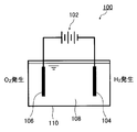
- the cathode electrode 104 and the anode electrode 106 are installed in a container 110 filled with water 108. In this case, assuming that the electromotive force per one element of the photoelectric conversion element is 0.8 V, it is 1.6 V in two series, and water cannot be electrolyzed.
- An object of the present invention is to provide a water electrolysis system capable of solving the problems based on the above-described prior art, adjusting the voltage required for water electrolysis and reducing surplus power.
- the present invention is a water electrolysis system that decomposes an aqueous electrolyte solution into hydrogen and oxygen by light, having at least one photoelectric conversion element, receiving light and receiving power.
- the electrolysis of water wherein the photoelectric conversion unit and the electrolyte cell are electrically connected in series, and the photoelectric conversion unit or the electrolyte cell located at each end in the arrangement state is electrically connected A system is provided.
- the photoelectric conversion unit is disposed on the surface of the insulating substrate, and the electrolyte cell is disposed on the back surface of the insulating substrate on the side opposite to the side on which the photoelectric conversion unit receives light, and serves as a gas generating electrode. It is preferable that a hydrogen generating electrode for generating gas and an oxygen generating electrode for generating oxygen gas are provided, and the hydrogen generating electrode and the oxygen generating electrode are opposed to each other.
- the photoelectric conversion unit is preferably a unit in which a plurality of photoelectric conversion elements are connected in series.
- the photoelectric conversion element preferably includes an inorganic semiconductor film having a pn junction.
- the inorganic semiconductor film preferably has an absorption wavelength end of 800 nm or more.
- the inorganic semiconductor film includes a CIGS compound semiconductor or a CZTS compound semiconductor.
- the gas generating electrode is provided with a catalyst electrode used for generating hydrogen gas, and the catalyst electrode used for generating hydrogen gas is preferably composed of Pt, Pt-containing material, or Rh.
- a catalyst electrode is provided in the oxygen gas generation unit, a catalyst electrode used for generation of oxygen gas is provided in the gas generation electrode, and the catalyst electrode used for generation of oxygen gas is composed of CoO x or IrO 2. It is preferable.
- the amount of current generated in each photoelectric conversion unit is equal.
- the present invention it is possible to adjust a voltage applied to an electrolyte cell in which an aqueous electrolyte solution is electrolyzed to generate hydrogen gas and oxygen gas, and it is possible to reduce a loss of an overvoltage of a voltage required for water electrolysis. it can.
- a voltage applied to an electrolyte cell in which an aqueous electrolyte solution is electrolyzed to generate hydrogen gas and oxygen gas it is possible to reduce a loss of an overvoltage of a voltage required for water electrolysis. it can.
- by separating the photoelectric conversion unit and the gas generating electrode it is not necessary to immerse the photoelectric conversion part in the aqueous electrolyte solution, and performance degradation due to immersion can be avoided.
- the electrolysis of water is performed in the electrolyte cell to obtain hydrogen gas and oxygen gas, the area of the electrolyte cell can be reduced.
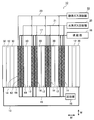
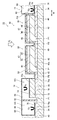
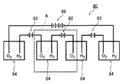
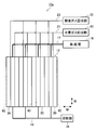
- FIG. 1 is a schematic plan view showing a water electrolysis system according to a first embodiment of the present invention. It is typical sectional drawing of the principal part of the water electrolysis system of the 1st Embodiment of this invention shown in FIG. 1 is an equivalent circuit diagram of a water electrolysis system according to a first embodiment of the present invention. It is a typical top view which shows the electrolysis system of the water of the 2nd Embodiment of this invention. It is typical sectional drawing of the principal part of the water electrolysis system of the 2nd Embodiment of this invention shown in FIG. (A) is an equivalent circuit diagram of the water electrolysis system of the embodiment of the present invention, and (b) is an equivalent circuit diagram of another example of the water electrolysis system of the embodiment of the present invention. It is a schematic diagram which shows the conventional electrolysis apparatus of water.
- FIG. 1 is a schematic plan view showing a water electrolysis system according to a first embodiment of the present invention
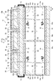
- FIG. 2 shows a water electrolysis system according to the first embodiment of the present invention shown in FIG. It is typical sectional drawing of the principal part.
- the water electrolysis system 10 (hereinafter simply referred to as the system 10) includes, for example, a plurality of photoelectric conversion units 12 and a plurality of electrolyte cells 14.
- the electrolyte cell 14 is disposed in the direction M between the photoelectric conversion units 12, and the photoelectric conversion unit 12 and the electrolyte cell 14 are electrically connected in series.
- the photoelectric conversion units 12 positioned at each end in the direction M are connected by, for example, a wiring 13. Note that the photoelectric conversion units 12 located at each end are not limited to being connected via the wiring 13.
- the photoelectric conversion unit 12 receives light and generates electric power, electric power for generating hydrogen gas in a hydrogen gas generating unit 32 described later, and electric power for generating oxygen gas in an oxygen gas generating unit 34 described later. It is for supplying.
- the electric power generated in the photoelectric conversion unit 12 includes a generated voltage and a generated current.
- the photoelectric conversion unit 12 has at least one photoelectric conversion element 30. As will be described later, in the example shown in FIGS. 1 and 2, the photoelectric conversion unit 12 is a cascade type integrated element in which two or more photoelectric conversion elements 30 are electrically connected in series.
- the electrolyte cell 14 is supplied with an aqueous electrolyte solution AQ as described later.
- the electrolyte aqueous solution AQ is decomposed using the electromotive force generated in the photoelectric conversion unit 12, and hydrogen gas and oxygen gas are generated in the electrolyte cell 14.
- the electrolyte cell 14 includes a hydrogen electrolyte cell that generates hydrogen and an oxygen electrolyte cell that generates oxygen, which are separated by a partition wall 62.
- the electrolyte cell 14 constitutes a gas generation region.
- the aqueous electrolyte solution AQ is, for example, a liquid containing H 2 O as a main component, and may be distilled water, or an aqueous solution containing water as a solvent and containing a solute.
- water for example, it may be an electrolytic solution that is an aqueous solution containing an electrolyte, or may be cooling water used in a cooling tower or the like.
- an aqueous solution containing an electrolyte such as a strong alkali (KOH), a polymer electrolyte (Nafion (registered trademark)), an electrolytic solution containing 0.1 M H 2 SO 4 , 0.1 M sodium sulfate.
- electrolytic solution 0.1M potassium phosphate buffer, etc.
- the system 10 includes a supply unit 16 for supplying the electrolyte aqueous solution AQ to the electrolyte cell 14 and a recovery unit 18 for recovering the electrolyte aqueous solution AQ discharged from the electrolyte cell 14.
- a known water supply device such as a pump can be used, and a known water recovery device such as a tank can be used.
- the supply unit 16 is connected to the electrolyte cell 14 via a supply pipe 17, and the recovery unit 18 is connected to the electrolyte cell 14 via a recovery pipe 19.
- the electrolyte aqueous solution AQ recovered by the recovery unit 18 may be circulated to the supply unit 16 so that the electrolyte aqueous solution AQ can be reused.
- the system 10 includes a hydrogen gas recovery unit 20 that recovers the hydrogen gas generated in the electrolyte cell 14 and an oxygen gas recovery unit 22 that recovers the oxygen gas generated in the electrolyte cell 14.
- the hydrogen gas recovery unit 20 is connected to the electrolyte cell 14 via a hydrogen pipe 21, and the oxygen gas recovery unit 22 is connected to the electrolyte cell 14 via an oxygen pipe 23.
- the configuration of the hydrogen gas recovery unit 20 is not particularly limited as long as the hydrogen gas can be recovered.
- an apparatus using an adsorption method, a diaphragm method, or the like can be used.
- the configuration of the oxygen gas recovery unit 22 is not particularly limited as long as the oxygen gas can be recovered.
- an apparatus using an adsorption method can be used.
- the system 10 may be inclined at a predetermined angle with respect to the width direction W.
- the system 10 is an integrated structure in which the photoelectric conversion unit 12 and the electrolyte cell 14 are provided on the surface 40a of the planar insulating substrate 40, that is, on the same plane.
- the surface 40a side of the insulating substrate 40 is the light receiving surface side of the photoelectric conversion unit.
- the photoelectric conversion unit 12 and the electrolyte cell 14 are electrically connected in series via the back electrode 42.
- the photoelectric conversion unit 12 includes, for example, two photoelectric conversion elements 30 connected in series, and is disposed on the surface 40 a of the insulating substrate 40.
- the photoelectric conversion element 30 is configured by laminating a back electrode 42, a photoelectric conversion layer 44, a buffer layer 46, a transparent electrode 48, and a protective film 50 in order from the insulating substrate 40 side.
- a pn junction is formed at the interface between the photoelectric conversion layer 44 and the buffer layer 46.
- the photoelectric conversion layer 44 and the buffer layer 46 constitute an inorganic semiconductor film 47 having a pn junction.
- the protective film 50 is insoluble in a weakly acidic solution and a weakly alkaline solution, and also has light transmission properties, water shielding properties, and insulating properties. Since the protective film 50 has translucency and protects the photoelectric conversion element 30, the protective film 50 covers the entire surface of the transparent electrode 48 and the side surface 49 of the photoelectric conversion element 30.
- Protective film 50 for example, a SiO 2, SnO 2, Nb 2 O 5, Ta 2 O 5, Al 2 O 3 and Ga 2 O 3 or the like.
- the thickness of the protective film 50 is not particularly limited and is preferably 100 to 1000 nm.
- the formation method of the protective film 50 is not specifically limited, It can form by RF sputtering method, DC reactive sputtering method, MOCVD method, etc.
- the protective film 50 can be made of, for example, an insulating epoxy resin, an insulating silicone resin, an insulating fluororesin, or the like.
- the thickness of the protective film 50 is not particularly limited and is preferably 2 to 1000 ⁇ m.
- two photoelectric conversion elements 30 are connected in series in the direction M.
- the number is limited as long as an electromotive force capable of generating hydrogen gas and oxygen gas can be obtained. Instead, it may be one or three or more. It is possible to connect a plurality of photoelectric conversion elements 30 in series because a higher voltage can be obtained and a voltage generated in the entire system 10 can be adjusted by connecting the plurality of photoelectric conversion elements 30 in series. preferable.
- a hydrogen gas generation unit 32 and an oxygen gas generation unit 34 are arranged in the direction M across the photoelectric conversion unit 12, and the photoelectric conversion unit 12, the hydrogen gas generation unit 32, and the oxygen gas generation unit 34 are electrically connected in series. It is connected.
- the electrolyte cell 14 is formed of a container 60 provided on the insulating substrate 40.
- the partition wall 62 provided in the container 60 forms a hydrogen electrolyte cell 64 and an oxygen electrolyte cell 66.
- the configuration of the container 60 is not particularly limited as long as it can accommodate the electrolyte aqueous solution AQ without leaking and does not react with hydrogen gas and oxygen gas.
- the hydrogen gas generation unit 32 disposed in the hydrogen electrolyte cell 64 and the oxygen gas generation unit 34 disposed in the oxygen electrolyte cell 66 are respectively connected to different photoelectric conversion units 12.
- the hydrogen gas generation unit 32 and the oxygen gas generation unit 34 of the adjacent photoelectric conversion unit 12 are disposed in the same electrolyte cell 14.
- the partition wall 62 is for isolating the hydrogen gas generated in the hydrogen electrolyte cell 64 and the oxygen gas generated in the oxygen electrolyte cell 66 so as not to be mixed. Therefore, the configuration of the partition wall 62 is not particularly limited as long as it has the isolation function described above.
- the partition wall 62 includes hydroxide ions (PH also increases) that are increased by the generation of hydrogen in the hydrogen electrolyte cell 64 and hydrogen ions (PH is decreased) that is increased by the generation of oxygen in the oxygen electrolyte cell 66.
- the container 60 may be separated from the hydrogen electrolyte cell 64 and the oxygen electrolyte cell 66 in order to allow hydroxide ions and hydrogen ions to pass therethrough.
- the partition wall 62 is made of, for example, a material having ion permeability and gas non-permeability. Specifically, for example, it is composed of an ion exchange membrane, a ceramic filter, porous glass, or the like.
- the thickness of the partition wall 62 is not particularly limited, and is preferably 10 to 1000 ⁇ m.
- the hydrogen gas generation unit 32 includes a region 70 where the back electrode 42 connected to the photoelectric conversion element 30 extends, a functional layer 72 formed on the surface 70a of the region 70, and a catalyst electrode 74 for promoting hydrogen generation. And have.
- a catalyst electrode 74 used for generating hydrogen gas is formed on the surface 72 a of the functional layer 72.
- the functional layer 72 constitutes the hydrogen gas generation unit 32, and a transparent conductive protective film is used. Further, the functional layer 72 is insoluble in the weakly acidic solution and the weakly alkaline solution, and also has light transmittance, water shielding properties, and conductivity.
- the functional layer 72 supplies electrons to hydrogen ions (protons) H + ionized from water molecules to generate hydrogen molecules, that is, hydrogen gas (2H + + 2e ⁇ ⁇ > H 2 ), and has a surface 72a. Functions as a hydrogen gas generating surface. Therefore, the functional layer 72 constitutes a hydrogen gas generation region.
- a transparent conductive film similar to the transparent electrode 48 such as ZnO doped with ITO, Al, B, Ga, In, or the like, or IMO (In 2 O 3 doped with Mo) is used. be able to.
- the functional layer 72 may have a single-layer structure or a laminated structure such as a two-layer structure.
- the thickness of the functional layer 72 is not particularly limited, and is preferably 10 to 1000 nm, and more preferably 50 to 500 nm.
- the method for forming the functional layer 72 is not particularly limited, as with the transparent electrode 48, and may be formed by a vapor deposition method such as an electron beam evaporation method, a sputtering method, or a CVD method, or a coating method. it can.
- the catalyst electrode 74 a metal, a conductive oxide, or a substance having an overvoltage of less than 0.5V is used. More specifically, the catalyst electrode 74 is composed of, for example, a simple substance composed of Pt, Pd, Ni, Fe, Au, Ag, Ru, Cu, Co, Rh, Ir, Mn, and an alloy combining them. and oxides thereof, for example, NiOx and RuO 2.
- the size of the catalyst electrode 74 is not particularly limited, and is preferably 5 nm to 1 ⁇ m.
- the formation method of the catalyst electrode 74 is not specifically limited, It can form by the application
- the functional layer 72 is not necessarily provided, and the catalyst electrode 74 may be directly formed on the surface 70 a of the region 70.
- the region 70 obtained by extending the back electrode 42 functions as a hydrogen generation electrode
- the surface 70a functions as a hydrogen gas generation surface.
- the oxygen gas generation unit 34 is configured by a region 76 that is an extension of the back electrode 42 of the photoelectric conversion element 30, and this region 76 forms an oxygen gas generation region and functions as an oxygen generation electrode.
- the region 76 of the extended portion of the back electrode 42 of the photoelectric conversion element 30 takes out electrons from the hydroxide ions OH ⁇ ionized from the water molecules and generates oxygen molecules, that is, oxygen gas (2OH ⁇ ⁇ ). > H 2 O + O 2/ 2 + 2e -) are those, the surface 76a serves as oxygen gas generating surface.
- a catalyst electrode 78 for oxygen generation used for generating oxygen gas is formed on the surface 76a of the region 76 of the back electrode 42.
- the catalyst electrode 78 for generating oxygen is made of a metal, a conductive oxide, or a substance having an overvoltage of less than 0.5V. More specifically, the catalyst electrode 78 is composed of, for example, IrO 2, Ni, Co, Pt , Fe, by CoO x, or the like.
- the size of the catalyst electrode 78 for generating oxygen is not particularly limited, and is preferably 5 nm to 1 ⁇ m.
- the method for forming the catalyst electrode 78 for generating oxygen is not particularly limited, and can be formed by a coating and baking method, a dipping method, an impregnation method, a sputtering method, a vapor deposition method, or the like.
- the hydrogen generation electrode and the oxygen generation electrode are collectively referred to as a gas generation electrode.
- the insulating substrate 40 is not particularly limited as long as it has an insulating property and has a strength capable of supporting the photoelectric conversion unit 12 and the electrolyte cell 14.
- a soda lime glass (SLG) substrate or a ceramic substrate can be used as the insulating substrate 40.
- the insulating substrate 40 may be a metal substrate having an insulating layer formed thereon.
- a metal substrate such as an Al substrate or a SUS substrate, or a composite metal substrate such as a composite Al substrate made of a composite material of Al and another metal such as SUS can be used.
- the composite metal substrate is also a kind of metal substrate, and the metal substrate and the composite metal substrate are collectively referred to simply as a metal substrate.
- a metal substrate with an insulating film having an insulating layer formed by anodizing the surface of an Al substrate or the like can also be used.
- the insulating substrate 40 may or may not be flexible.
- a glass plate such as high strain point glass and non-alkali glass, or a polyimide material can be used as the insulating substrate 40.
- the thickness of the insulating substrate 40 is not particularly limited as long as the photoelectric conversion unit 12 and the electrolyte cell 14 can be supported, and may be any thickness, for example, about 20 to 20000 ⁇ m. Is preferably ⁇ 10,000 ⁇ m, more preferably 1000 to 5,000 ⁇ m.
- the back electrode 42 is made of, for example, a metal such as Mo, Cr, or W, or a combination thereof.
- the back electrode 42 may have a single layer structure or a laminated structure such as a two-layer structure. Among these, the back electrode 42 is preferably composed of Mo.
- the thickness of the back electrode 42 is generally about 800 nm, but the thickness of the back electrode 42 is preferably 400 nm to 1 ⁇ m.
- the photoelectric conversion layer 44 forms a pn junction in which the photoelectric conversion layer 44 side is p-type and the buffer layer 46 side is n-type at the interface with the buffer layer 46. It is a layer that absorbs light that has passed through the protective film 50, the transparent electrode 48, and the buffer layer 46 and generates holes on the p side and electrons on the n side, and has a photoelectric conversion function.
- holes generated in the pn junction are moved from the photoelectric conversion layer 44 to the back electrode 42 side, and electrons generated in the pn junction are moved from the buffer layer 46 to the transparent electrode 48 side.
- the film thickness of the photoelectric conversion layer 44 is preferably 1.0 to 3.0 ⁇ m, and particularly preferably 1.5 to 2.0 ⁇ m.
- the photoelectric conversion layer 44 is preferably composed of, for example, a CIGS compound semiconductor or a CZTS compound semiconductor having a chalcopyrite crystal structure. That is, the photoelectric conversion layer 44 is preferably composed of a CIGS compound semiconductor layer.
- the CIGS compound semiconductor layer may be formed of not only Cu (In, Ga) Se 2 (CIGS) but also known materials used for CIGS systems such as CuInSe 2 (CIS) and CuGaSe 2 (CGS). Good.
- CIGS layer forming methods 1) multi-source vapor deposition, 2) selenization, 3) sputtering, 4) hybrid sputtering, and 5) mechanochemical process are known.
- CIGS layer forming methods include screen printing, proximity sublimation, MOCVD, and spray (wet film formation).
- a fine particle film containing an Ib group element, a IIIb group element, and a VIb group element is formed on a substrate by a screen printing method (wet film forming method) or a spray method (wet film forming method), and then pyrolyzed ( At this time, a crystal having a desired composition can be obtained by performing a thermal decomposition treatment in a VIb group element atmosphere (JP-A-9-74065, JP-A-9-74213, etc.).
- the photoelectric conversion layer 44 is preferably composed of, for example, a CIGS compound semiconductor or a CZTS compound semiconductor having a chalcopyrite crystal structure, but is not limited thereto, and is not limited thereto. Any photoelectric conversion element may be used as long as it can form a pn junction consisting of the above, generate a photodecomposition reaction of water, and generate hydrogen gas and oxygen gas.
- the photoelectric conversion element used for the photovoltaic cell which comprises a solar cell is used preferably.
- Such photoelectric conversion elements include CIGS thin film photoelectric conversion elements, CIS thin film photoelectric conversion elements, and CZTS thin film photoelectric conversion elements, as well as thin film silicon thin film photoelectric conversion elements and CdTe thin film photoelectric conversion elements. Examples thereof include a conversion element, a dye-sensitized thin film photoelectric conversion element, and an organic thin film photoelectric conversion element.
- the absorption wavelength of the inorganic semiconductor that forms the photoelectric conversion layer 44 is not particularly limited as long as it is a wavelength region in which photoelectric conversion is possible.
- the absorption wavelength end As an absorption wavelength, it is only necessary to include a wavelength region such as sunlight, in particular, a visible wavelength region to an infrared wavelength region, but the absorption wavelength end includes 800 nm or more, that is, the infrared wavelength region. Is preferred. The reason is that as much solar energy as possible can be used.
- the longer absorption wavelength end corresponds to the reduction of the band gap, which can be expected to reduce the electromotive force for assisting water decomposition. Therefore, it can be expected that the number of connections connected in series will increase. Therefore, the longer the absorption edge, the better.
- the buffer layer 46 constitutes the inorganic semiconductor film 47 having a pn junction together with the photoelectric conversion layer 44 as described above.
- the buffer layer 46 is formed to protect the photoelectric conversion layer 44 when the transparent electrode 48 is formed and to transmit light incident on the transparent electrode 48 to the photoelectric conversion layer 44.
- the buffer layer 46 may be, for example, CdS, ZnS, Zn (S, O), and / or Zn (S, O, OH), SnS, Sn (S, O), and / or Sn (S, O, OH).
- the thickness of the buffer layer 46 is preferably 10 nm to 2 ⁇ m, and more preferably 15 to 200 nm.
- the buffer layer 46 is formed by, for example, a chemical bath deposition method (hereinafter referred to as CBD method).
- a window layer may be provided between the buffer layer 46 and the transparent electrode 48. This window layer is composed of, for example, a ZnO layer having a thickness of about 10 nm.
- the transparent electrode 48 has translucency, takes light into the photoelectric conversion layer 44, and moves the holes and electrons generated in the photoelectric conversion layer 44 in pairs with the back electrode 42 (current flows). ) Functions as an electrode and functions as a transparent conductive film for connecting two photoelectric conversion elements 30 in series.
- the transparent electrode 48 is made of, for example, ZnO doped with Al, B, Ga, In, or the like, or ITO.
- the transparent electrode 48 may have a single layer structure or a laminated structure such as a two-layer structure. Further, the thickness of the transparent electrode is not particularly limited and is preferably 0.3 to 1 ⁇ m.
- the formation method of a transparent electrode is not specifically limited, It can form by vapor phase film-forming methods, such as an electron beam vapor deposition method, a sputtering method, and CVD method, or the apply
- the transparent conductive film for connecting adjacent photoelectric conversion elements 30 in series is not limited to the transparent electrode 48, but is formed simultaneously with the same transparent conductive film as the transparent electrode 48 for ease of manufacturing. It is good. That is, after the buffer layer 46 is laminated on the photoelectric conversion layer 44, the opening groove P2 reaching the surface of the back electrode 42 is formed by laser scribe or mechanical scribe, and the opening groove P2 is filled on the buffer layer 46. Then, the transparent conductive film constituting the transparent electrode 48 is formed, and thereafter, the transparent conductive film in each opening groove P2 is removed by scribing, and the opening groove P2 having a slightly narrow width reaching the surface of the back electrode 42 is formed again. By leaving the back electrode 42 of the adjacent photoelectric conversion element 30 and the transparent electrode 48 as a conductive film that directly connects, a conductive film for connecting the adjacent photoelectric conversion elements 30 in series can be formed.
- the photoelectric conversion unit 12 when light L enters the photoelectric conversion element 30 from the protective film 50 side, the light L passes through the protective film 50, each transparent electrode 48, and each buffer layer 46, and each photoelectric conversion layer An electromotive force is generated at 44, and for example, a current (movement of holes) from the transparent electrode 48 toward the back electrode 42 is generated. For this reason, in the photoelectric conversion unit 12, the hydrogen gas generation part 32 becomes a negative electrode (electrolysis cathode), and the oxygen gas generation part 34 becomes a positive electrode (electrolysis anode). Note that the type (polarity) of the generated gas in the photoelectric conversion unit 12 is appropriately changed according to the configuration of the photoelectric conversion element 30, the configuration of the photoelectric conversion unit 12, and the like.
- the manufacturing method of the photoelectric conversion unit 12 is not limited to the manufacturing method shown below.
- a soda lime glass substrate to be the insulating substrate 40 is prepared.
- a Mo film or the like to be the back electrode 42 is formed on the surface of the insulating substrate 40 by a sputtering method using a film forming apparatus.
- a predetermined position of the Mo film is scribed to form a separation groove P1 extending in the width direction W (see FIG. 1) of the insulating substrate 40.
- the back surface electrodes 42 separated from each other by the separation groove P1 are formed.
- a CIGS film (p-type semiconductor layer) is formed as the photoelectric conversion layer 44 so as to cover the back electrode 42 and fill the separation groove P1.
- This CIGS film is formed by any of the film forming methods described above.
- a CdS layer (n-type semiconductor layer) to be the buffer layer 46 is formed on the photoelectric conversion layer 44 by the CBD method.
- the direction M it extends in the width direction W (see FIG. 1) of the insulating substrate 40 at a position different from the position where the separation groove P1 is formed, and the back electrode 42 extends from the buffer layer 46 through the photoelectric conversion layer 44.
- Two opening grooves P2 reaching the surface are formed by, for example, a scribe method. In this case, a laser scribe method or a mechanical scribe method can be used as the scribe method.
- the transparent electrode 48 is formed so as to extend in the width direction W (see FIG. 1) of the insulating substrate 40 and fill the opening groove P2 on the buffer layer 46.
- the opening groove P2 For example, Al, B, Ga, Sb, etc.
- a ZnO: Al layer to which is added is formed by sputtering or coating.
- the ZnO: Al layer in the opening groove P2 is removed so as to leave a part, and two slightly narrow opening grooves P2 reaching the surface of the back electrode 42 are formed again by, for example, a scribe method. Also in this case, a laser scribe method or a mechanical scribe method can be used as the scribe method.
- a protective film 50 is formed on the outer surface of the photoelectric conversion element 30 constituting the photoelectric conversion unit 12, the surface of the back electrode 42 on the bottom surface of the two opening grooves P2, and the side surface 49 of the photoelectric conversion element 30, for example, SiO Two films are formed by RF sputtering. Thereby, the two photoelectric conversion elements 30 can be formed.
- the deposit formed by the above-described process at the position where the electrolyte cell 14 is set in advance is removed using, for example, a laser scribe method or a mechanical scribe method, and the hydrogen gas generation unit 32 is configured.
- the region 70 of the back electrode 42 to be exposed and the region 76 of the back electrode 42 constituting the oxygen gas generator 34 are exposed.
- the region 70 and the region 76 are obtained by extending the back electrodes 42 of the photoelectric conversion elements 30 of the different photoelectric conversion units 12.
- a Pt catalyst electrode for example, which becomes the catalyst electrode 74 for hydrogen generation by a photo-deposition method is supported.
- a CoO x catalyst electrode to be a catalyst electrode 78 for oxygen generation is carried on the surface 76a of the region 76 to be the oxygen gas generation unit 34 by, for example, an immersion method.
- the partition wall 62 is installed in the separation groove P ⁇ b> 1 between the region 70 and the region 76.
- the container 60 which comprises the electrolyte cell 14 is prepared, and this container 60 is arrange
- the electrolyte cell 14 having the hydrogen electrolyte cell 64 and the oxygen electrolyte cell 66 separated by the partition wall 62 is formed.
- the supply pipe 17, the recovery pipe 19, the hydrogen pipe 21, and the oxygen pipe 23 are connected to the electrolyte cell 14, and these are connected to the supply section 16, the recovery section 18, the hydrogen gas recovery section 20, and the oxygen gas recovery, respectively. By setting it as the part 22, the system 10 can be manufactured.
- the photoelectric conversion unit 12 is irradiated with light L, and the electrolyte aqueous solution AQ is supplied from the supply unit 16 to each electrolyte cell 14. Accordingly, the aqueous electrolyte solution AQ is decomposed in the hydrogen electrolyte cell 64 of each electrolyte cell 14 to generate hydrogen gas, and the aqueous electrolyte solution AQ is decomposed in the oxygen electrolyte cell 66 to generate oxygen gas.
- the hydrogen gas is recovered by the hydrogen gas recovery unit 20 through the hydrogen pipe 21.
- the oxygen gas is recovered by the oxygen gas recovery unit 22 through the oxygen pipe 23.
- the system 10 by separating the photoelectric conversion unit 12 and the gas generating electrode, it is not necessary to immerse the photoelectric conversion part in the aqueous electrolyte solution AQ, and performance degradation due to immersion can be avoided. Further, since the aqueous electrolyte solution AQ is electrolyzed in the electrolyte cell 14 to obtain hydrogen gas and oxygen gas, the area of the electrolyte cell 14 can be reduced.
- the system 10 can be represented as an equivalent circuit 80 as shown in FIG.
- the power supply unit 82 corresponds to the photoelectric conversion unit 12 shown in FIG. 1
- the electrolyte cell unit 84 corresponds to the electrolyte cell 14 shown in FIG.
- the electromotive force part 86 connected to the electrolyte cell part 84 of both ends is equivalent to what the photoelectric conversion element 30 of the photoelectric conversion unit 12 of both ends shown in FIG.
- One battery of the power supply unit 82 and the electromotive force unit 86 corresponds to one photoelectric conversion element 30.
- the area A of the equivalent circuit 80 corresponds to the main part of the water electrolysis system shown in FIG.
- the plurality of photoelectric conversion units 12 preferably have the same amount of generated current and generated voltage in each photoelectric conversion unit 12 when irradiated with light. However, since the voltage obtained by dividing the voltage of the entire system 10 by the number of the electrolyte cells 14 is applied to the electrolyte cell 14, even if there is a plurality of photoelectric conversion units 12 whose voltage is equal to or lower than a predetermined voltage. The other photoelectric conversion unit 12 can compensate for the voltage drop.
- FIG. 4 is a schematic plan view showing a water electrolysis system according to a second embodiment of the present invention.
- FIG. 5 is a schematic cross-sectional view of a main part of the water electrolysis system according to the second embodiment of the present invention shown in FIG.
- FIG. 6A is an equivalent circuit diagram of the water electrolysis system of the embodiment of the present invention
- FIG. 6B is an equivalent circuit diagram of another example of the water electrolysis system of the embodiment of the present invention. is there.
- the same components as those of the water electrolysis system 10 of the first embodiment shown in FIGS. 1 and 2 and the same components as the equivalent circuit 80 shown in FIG. Detailed description thereof will be omitted.
- the water electrolysis system 10a of the present embodiment (hereinafter simply referred to as the system 10a) is a surface of a planar insulating substrate 40 as compared to the system 10 of the first embodiment.
- the difference is that only the photoelectric conversion unit 12 is disposed on the surface 40a of the insulating substrate 40, not the integrated structure in which the photoelectric conversion unit 12 and the electrolyte cell 14 are provided on 40a.
- the electrolyte cell 14a is provided not on the surface 40a of the insulating substrate 40 but on the back surface 40b of the insulating substrate 40 opposite to the side on which the photoelectric conversion unit 12 receives light.
- the difference is that not the photoelectric conversion elements 30 of the photoelectric conversion unit 12 positioned at each end in the direction M but the back electrodes 42 a and 42 b and the electrolyte cell 14 a are connected by the wiring 13. Furthermore, as shown in FIG. 4, the connection positions of the supply pipe 17, the recovery pipe 19, the hydrogen pipe 21, and the oxygen pipe 23 are different. Except for these points, the system 10a has the same configuration as the system 10 shown in FIGS.
- a flat insulating base material 90 is disposed in parallel with the back surface 40b of the insulating substrate 40 so as to face the back surface 40b of the insulating substrate 40.
- a plurality of wall materials 92 are provided between the back surface 40b of the insulating substrate 40 and the front surface 90a of the insulating base material 90, and in the example of FIG. 5, three wall materials 92 are provided. Thereby, two electrolyte cells 14a are formed.
- the electrolyte cell 14a constitutes a gas generation region.
- each electrolyte cell 14a a gas separation film 63 is provided between the insulating substrate 40 and the insulating base material 90 in parallel with the back surface 40b of the insulating substrate 40 and the front surface 90a of the insulating base material 90.
- the electrolyte cell 64 for hydrogen and the electrolyte cell 66 for oxygen are isolate
- the hydrogen electrolyte cell 64 is connected to the hydrogen gas recovery unit 20 via the hydrogen pipe 21.
- the oxygen electrolyte cell 66 is connected to the oxygen gas recovery unit 22 via the oxygen tube 23.
- the supply unit 16 is connected to the hydrogen electrolyte cell 64 and the oxygen electrolyte cell 66 via the supply pipe 17 and supplied with the aqueous electrolyte solution AQ.
- the back electrode 42a is a negative electrode (electrolysis cathode), and the back electrode 42b is a positive electrode (electrolysis anode). Therefore, the electrolyte cell 14a on the back electrode 42a side is the hydrogen electrolyte cell 64 on the insulating substrate 40 side.
- a hydrogen generation electrode 94 is provided on the back surface 40 b of the insulating substrate 40.
- the hydrogen generation electrode 94 is electrically connected to the back surface electrode 42 a by the wiring 13.
- a catalyst electrode 74 for generating hydrogen is formed on the surface 94 a of the hydrogen generating electrode 94. Thereby, the hydrogen gas production
- the electrolyte cell 14a on the back electrode 42a side is the oxygen electrolyte cell 66 on the insulating base material 90 side.
- the electrolyte cell 14a on the back electrode 42b side is an oxygen electrolyte cell 66 on the insulating substrate 40 side.
- an oxygen generation electrode 95 is provided on the back surface 40 b of the insulating substrate 40.
- the oxygen generating electrode 95 is electrically connected to the back surface electrode 42 b by the wiring 13.
- a catalyst electrode 78 for generating oxygen is formed on the surface 95 a of the oxygen generating electrode 95.
- the electrolyte cell 14a on the back electrode 42b side is the hydrogen electrolyte cell 64 on the insulating substrate 90 side.
- a common conductive member 96 is provided in the hydrogen electrolyte cell 64 and the oxygen electrolyte cell 66 on the insulating base material 90 side.
- the common conductive member 96 is disposed on the surface 90a of the insulating substrate 90.
- the common conductive member 96 is grounded.
- a catalyst electrode 74 for generating hydrogen is formed on a surface 96b corresponding to the electrolyte cell 64 for hydrogen.
- a catalyst electrode 78 for oxygen generation is formed on the surface 96 a of the common conductive member 96 corresponding to the oxygen electrolyte cell 66.
- the common conductive member 96 serves as both a hydrogen gas generation electrode and an oxygen gas generation electrode. In this way, the hydrogen gas generation unit 32 and the oxygen gas generation unit 34 are configured in the hydrogen electrolyte cell 64 and the oxygen electrolyte cell 66, respectively.
- the electrolyte cell 14a includes the hydrogen generation electrode 94 for generating hydrogen gas and the oxygen generation electrode 95 for generating oxygen gas as gas generation electrodes. Both the hydrogen generation electrode 94 and the oxygen generation electrode 95 are made of a flat conductor. The hydrogen generation electrode 94 and the oxygen generation electrode 95 are opposed to each other with the gas separation film 63 interposed therebetween, and are provided in parallel with the back surface 40 b of the insulating substrate 40.
- hydrogen gas is generated due to a potential difference between the hydrogen generation electrode 94 of the hydrogen electrolyte cell 64 and the common conductive member 96. Further, oxygen gas is generated by the potential difference between the oxygen generating electrode 95 and the common conductive member 96 of the oxygen electrolyte cell 66.
- the gas separation membrane 63 provided in each electrolyte cell 14a is increased by hydroxyl ions (PH also increases) generated by the generation of hydrogen in the hydrogen electrolyte cell 64 and oxygen generation in the oxygen electrolyte cell 66.
- PH hydroxyl ions
- the gas separation membrane 63 is made of, for example, a material having ion permeability and gas non-permeability. Specifically, for example, it is composed of an ion exchange membrane, a ceramic filter, porous glass, or the like.
- the thickness of the gas separation membrane 63 is not particularly limited, and is preferably 10 to 1000 ⁇ m.
- each electrolyte cell 14a can be formed of the same material as the insulating substrate 40, detailed description thereof is omitted.
- the configuration of the wall member 92 is not particularly limited as long as it can accommodate the electrolyte aqueous solution AQ without leaking and does not react with hydrogen gas and oxygen gas. Since the hydrogen generation electrode 94, the oxygen generation electrode 95, and the common conductive member 96 can be configured in the same manner as the back electrode 42, detailed description thereof is omitted.
- the system 10a can be represented as an equivalent circuit 81 as shown in FIG.
- the electrolyte cell portion 84 corresponds to the electrolyte cell 14a shown in FIG.
- the electromotive force portion 86 connected to the electrolyte cell portion 84 corresponds to the photoelectric conversion unit 12 shown in FIG.
- One battery of the electromotive force unit 86 corresponds to one photoelectric conversion element 30.
- the wiring part 88 corresponds to the common conductive member 96 shown in FIG. In the system 10a, the electrolyte cells 14a are connected in series.
- the photoelectric conversion unit 12 is irradiated with light L, and the aqueous electrolyte solution AQ is supplied from the supply unit 16 to each electrolyte cell 14. Accordingly, the aqueous electrolyte solution AQ is decomposed in the hydrogen electrolyte cell 64 of each electrolyte cell 14 to generate hydrogen gas, and the aqueous electrolyte solution AQ is decomposed in the oxygen electrolyte cell 66 to generate oxygen gas.
- the hydrogen gas is recovered by the hydrogen gas recovery unit 20 through the hydrogen pipe 21.
- the oxygen gas is recovered by the oxygen gas recovery unit 22 through the oxygen pipe 23.
- the electrolyte cell 14a on the back surface 40b side of the insulating substrate 40 opposite to the light receiving surface, the area of the hydrogen electrolyte cell 64 and the oxygen electrolyte cell 66 can be increased, thereby generating hydrogen.
- the area of the electrode 94 and the oxygen generating electrode 95 can be increased. Thereby, the amount of gas generation can be increased.
- the effect similar to the system 10 other than the above can be acquired.
- the present invention is basically configured as described above. Although the water electrolysis system of the present invention has been described in detail above, the present invention is not limited to the above embodiment, and various improvements or modifications may be made without departing from the spirit of the present invention. Of course.
Landscapes
- Chemical & Material Sciences (AREA)
- Engineering & Computer Science (AREA)
- Chemical Kinetics & Catalysis (AREA)
- Electrochemistry (AREA)
- Materials Engineering (AREA)
- Metallurgy (AREA)
- Organic Chemistry (AREA)
- Inorganic Chemistry (AREA)
- Automation & Control Theory (AREA)
- Electrolytic Production Of Non-Metals, Compounds, Apparatuses Therefor (AREA)
- Power Engineering (AREA)
- Microelectronics & Electronic Packaging (AREA)
- Electrodes For Compound Or Non-Metal Manufacture (AREA)
Abstract
水の電気分解システムは、光により電解質水溶液を、水素と酸素に分解するものである。少なくとも1つの光電変換素子を有し、光を受光して電力を発生する、複数の光電変換ユニットと、光電変換ユニットで得られた電力により、電解質水溶液を電気分解して水素ガスと酸素ガスが生成される、複数の電解質セルとを有する。光電変換ユニットと電解質セルとは電気的に直列に接続されている。光電変換ユニット間に電解質セルが配置され、配置状態で各端に位置する光電変換ユニットまたは電解質セルが電気的に接続されている。
Description
本発明は、光電変換素子を用い、光を受光して水を電気分解し、水素と酸素に分解する水の電気分解システムに関し、特に、水の電気分解に要する電圧を調整することができる水の電気分解システムに関する。
従来、再生可能なエネルギーである太陽光エネルギーを利用する形態の1つとして、太陽電池に使用される光電変換材料を用いて、光電変換で得られる電子と正孔とを水の分解反応に利用して、燃料電池等に用いられる水素を製造する水素製造装置が提案されている(例えば、特許文献1参照)。
特許文献1に開示の水素製造装置は、太陽光が入射されると起電力を発生するpn接合を2つ以上直列にした光電変換部または太陽電池を設け、その上側の太陽光を受光する受光面とは逆の光電変換部または太陽電池の下側に電解液室を設け、電解室内をイオン伝導性隔壁または隔膜によって分け、太陽光の受光により光電変換部または太陽電池で発生する電力により、水を電解して水素を生成している。
特許文献1では、起電力0.9VのGaAs太陽電池と起電力1.7VのGaAs太陽電池を用いており、発生する電流値が等価であって、起電力の和が水の電解開始電圧以上、すなわち、水の電気分解に要する電圧以上とされている。
また、特許文献1では、太陽電池のp型およびn型半導体に接続された電極板をそれぞれ陽極および陰極として水を電解しているので、太陽エネルギーから水素への変換効率を高くすることができるとしている。
特許文献1では、起電力0.9VのGaAs太陽電池と起電力1.7VのGaAs太陽電池を用いており、発生する電流値が等価であって、起電力の和が水の電解開始電圧以上、すなわち、水の電気分解に要する電圧以上とされている。
また、特許文献1では、太陽電池のp型およびn型半導体に接続された電極板をそれぞれ陽極および陰極として水を電解しているので、太陽エネルギーから水素への変換効率を高くすることができるとしている。
特許文献1のように太陽光の受光により光電変換部または太陽電池で発生する電力により、水を電解して水素を生成することがなされている。
例えば、水の電気分解に要する電圧が1.8Vの場合、特許文献1のように、起電力0.9VのGsAs太陽電池と起電力1.7VのGaAs太陽電池を用いる場合、(0.9V+1.7V)-1.8V=0.8Vが余剰であり、0.8V分のエネルギーロスになる。
例えば、水の電気分解に要する電圧が1.8Vの場合、特許文献1のように、起電力0.9VのGsAs太陽電池と起電力1.7VのGaAs太陽電池を用いる場合、(0.9V+1.7V)-1.8V=0.8Vが余剰であり、0.8V分のエネルギーロスになる。
これ以外にも従来では、図7に示す従来の水の電気分解装置100のように、光電変換素子が直列されてなる電源部102の電圧を調整していた。この電圧の調整は、電源部102を構成する光電変換素子の直列数を変えることによりなされる。電源部102は、水素発生用のカソード電極104と酸素発生用のアノード電極106に接続されている。カソード電極104とアノード電極106は、水108が満たされた容器110に設置される。
この場合、光電変換素子の1素子当りの起電力を0.8Vとすると、2直列では1.6Vであり、水を電気分解することができない。一方、3直列では2.4Vとなり、0.6Vが余剰であり、0.6V分のエネルギーロスになる。
このように、水の実用的な電解開始電圧(水の電気分解に要する電圧)に対して最適な起電力を確保することは難しく、水の実用的な電解開始電圧以上の電圧分に相当する余剰電力は無駄になってしまうという問題点がある。
この場合、光電変換素子の1素子当りの起電力を0.8Vとすると、2直列では1.6Vであり、水を電気分解することができない。一方、3直列では2.4Vとなり、0.6Vが余剰であり、0.6V分のエネルギーロスになる。
このように、水の実用的な電解開始電圧(水の電気分解に要する電圧)に対して最適な起電力を確保することは難しく、水の実用的な電解開始電圧以上の電圧分に相当する余剰電力は無駄になってしまうという問題点がある。
本発明の目的は、前記従来技術に基づく問題点を解消し、水の電気分解に要する電圧を調整することができ、余剰電力を少なくできる水の電気分解システムを提供することにある。
上記目的を達成するために、本発明は、光により電解質水溶液を、水素と酸素に分解する水の電気分解システムであって、少なくとも1つの光電変換素子を有し、光を受光して電力を発生する、複数の光電変換ユニットと、光電変換ユニットで得られた電力により、電解質水溶液を電気分解して水素ガスと酸素ガスが生成されるガス発生電極を備える、複数の電解質セルとを有し、光電変換ユニットと電解質セルとは電気的に直列に接続されており、配置状態で各端に位置する光電変換ユニットまたは電解質セルが電気的に接続されていることを特徴とする水の電気分解システムを提供するものである。
また、光電変換ユニットは絶縁性基板の表面上に配置されており、電解質セルは光電変換ユニットが光を受光する側とは反対側の絶縁性基板の裏面上に配置され、ガス発生電極として水素ガスを生成するための水素発生電極と酸素ガスを生成するための酸素発生電極とを備え、水素発生電極と酸素発生電極とは対向していることが好ましい。
光電変換ユニットは、複数の光電変換素子が直列に接続されたものであることが好ましい。光電変換素子は、pn接合を有する無機半導体膜を備えることが好ましい。
無機半導体膜は、吸収波長端が800nm以上であることが好ましく、例えば、無機半導体膜はCIGS化合物半導体またはCZTS化合物半導体を含むものである。
光電変換ユニットは、複数の光電変換素子が直列に接続されたものであることが好ましい。光電変換素子は、pn接合を有する無機半導体膜を備えることが好ましい。
無機半導体膜は、吸収波長端が800nm以上であることが好ましく、例えば、無機半導体膜はCIGS化合物半導体またはCZTS化合物半導体を含むものである。
また、ガス発生電極に、水素ガスの生成に利用される触媒電極が設けられ、水素ガスの生成に利用される触媒電極は、Pt、Ptを含むもの、またはRhで構成されることが好ましい。酸素ガス生成部に触媒電極が設けられ、ガス発生電極に、酸素ガスの生成に利用される触媒電極が設けられ、酸素ガスの生成に利用される触媒電極は、CoOxまたはIrO2で構成されることが好ましい。
さらには、複数の光電変換ユニットは、光を照射された際、各光電変換ユニットで生じる発生電流量が等しいことが好ましい。
さらには、複数の光電変換ユニットは、光を照射された際、各光電変換ユニットで生じる発生電流量が等しいことが好ましい。
本発明によれば、電解質水溶液を電気分解して水素ガスと酸素ガスが生成される電解質セルにかかる電圧の調整が可能となり、水の電気分解に要する電圧の過電圧分の損失を少なくすることができる。
また、光電変換ユニットとガス発生電極を分けることで、電解質水溶液に光電変換部分を浸漬させる必要がなくなり、浸漬による性能低下を回避することができる。
さらには、電解質セルで、水の電気分解を行い、水素ガスと酸素ガスを得るため、電解質セルの領域を小さくすることができる。
また、光電変換ユニットとガス発生電極を分けることで、電解質水溶液に光電変換部分を浸漬させる必要がなくなり、浸漬による性能低下を回避することができる。
さらには、電解質セルで、水の電気分解を行い、水素ガスと酸素ガスを得るため、電解質セルの領域を小さくすることができる。
以下に、添付の図面に示す好適実施形態に基づいて、本発明の水の電気分解システムを詳細に説明する。
図1は、本発明の第1の実施形態の水の電気分解システムを示す模式的平面図であり、図2は、図1に示す本発明の第1の実施形態の水の電気分解システムの要部の模式的断面図である。
図1は、本発明の第1の実施形態の水の電気分解システムを示す模式的平面図であり、図2は、図1に示す本発明の第1の実施形態の水の電気分解システムの要部の模式的断面図である。
図1に示すように、水の電気分解システム10(以下、単にシステム10という。)は、例えば、複数の光電変換ユニット12と、複数の電解質セル14とを有する。
システム10においては、光電変換ユニット12間に電解質セル14が方向Mに配置されており、光電変換ユニット12と電解質セル14とは電気的に直列に接続されている。配置状態で、方向Mの各端に位置する光電変換ユニット12同士が、例えば、配線13で接続されている。なお、各端に位置する光電変換ユニット12同士は配線13を介して接続されることに限定されるものではない。
システム10においては、光電変換ユニット12間に電解質セル14が方向Mに配置されており、光電変換ユニット12と電解質セル14とは電気的に直列に接続されている。配置状態で、方向Mの各端に位置する光電変換ユニット12同士が、例えば、配線13で接続されている。なお、各端に位置する光電変換ユニット12同士は配線13を介して接続されることに限定されるものではない。
光電変換ユニット12は、光を受光して電力を発生させ、後述する水素ガス生成部32で水素ガスを発生させるための電力、および後述する酸素ガス生成部34で酸素ガスを発生させるための電力を供給するためのものである。光電変換ユニット12で発生する電力には、発生電圧および発生電流が含まれる。
光電変換ユニット12は、少なくとも1つの光電変換素子30を有するものである。後述するように図1、図2に示す例では、光電変換ユニット12は2以上の複数の光電変換素子30が電気的に直列に接続されたカスケード型集積化素子である。
光電変換ユニット12は、少なくとも1つの光電変換素子30を有するものである。後述するように図1、図2に示す例では、光電変換ユニット12は2以上の複数の光電変換素子30が電気的に直列に接続されたカスケード型集積化素子である。
電解質セル14には、後述するように電解質水溶液AQが供給される。電解質セル14では、光電変換ユニット12で発生した起電力を利用して、電解質水溶液AQを分解し、電解質セル14内で水素ガスと酸素ガスが生成される。電解質セル14は、水素を発生させる水素用電解質セルと、酸素を発生させる酸素用電解質セルとを備え、これらは隔壁62で隔離されている。電解質セル14はガス生成領域を構成する。
ここで、電解質水溶液AQとは、例えば、H2Oを主成分とする液体であり、蒸留水であってもよく、水を溶媒とし溶質を含む水溶液であってもよい。水の場合、例えば、電解質を含む水溶液である電解液であってもよく、冷却塔等で用いられる冷却水であってもよい。電解液の場合、例えば、電解質を含む水溶液であり、例えば、強アルカリ(KOH)、ポリマー電解質(ナフィオン(登録商標))、0.1MのH2SO4を含む電解液、0.1M硫酸ナトリウム電解液、0.1Mリン酸カリウム緩衝液等である。
ここで、電解質水溶液AQとは、例えば、H2Oを主成分とする液体であり、蒸留水であってもよく、水を溶媒とし溶質を含む水溶液であってもよい。水の場合、例えば、電解質を含む水溶液である電解液であってもよく、冷却塔等で用いられる冷却水であってもよい。電解液の場合、例えば、電解質を含む水溶液であり、例えば、強アルカリ(KOH)、ポリマー電解質(ナフィオン(登録商標))、0.1MのH2SO4を含む電解液、0.1M硫酸ナトリウム電解液、0.1Mリン酸カリウム緩衝液等である。
システム10は、電解質セル14に電解質水溶液AQを供給するための供給部16と、電解質セル14から排出される電解質水溶液AQを回収する回収部18とを有する。
供給部16および回収部18は、ポンプ等の公知の水の供給装置が利用可能であり、タンク等の公知の水の回収装置が利用可能である。
供給部16は供給管17を介して電解質セル14に接続されており、回収部18は回収管19を介して電解質セル14に接続されている。回収部18で回収された電解質水溶液AQを供給部16に循環させて、電解質水溶液AQを再利用してもよい。
さらに、システム10は、電解質セル14で生成された水素ガスを回収する水素ガス回収部20と、電解質セル14で生成された酸素ガスを回収する酸素ガス回収部22とを有する。
供給部16および回収部18は、ポンプ等の公知の水の供給装置が利用可能であり、タンク等の公知の水の回収装置が利用可能である。
供給部16は供給管17を介して電解質セル14に接続されており、回収部18は回収管19を介して電解質セル14に接続されている。回収部18で回収された電解質水溶液AQを供給部16に循環させて、電解質水溶液AQを再利用してもよい。
さらに、システム10は、電解質セル14で生成された水素ガスを回収する水素ガス回収部20と、電解質セル14で生成された酸素ガスを回収する酸素ガス回収部22とを有する。
水素ガス回収部20は水素用管21を介して電解質セル14に接続され、酸素ガス回収部22は酸素用管23を介して電解質セル14に接続されている。
水素ガス回収部20は、水素ガスを回収することができれば、その構成は、特に限定されるものではなく、例えば、吸着法および隔膜法等を用いた装置を利用することができる。
酸素ガス回収部22は、酸素ガスを回収することができれば、その構成は、特に限定されるものではなく、例えば、吸着法を用いた装置を利用することができる。
なお、システム10は、幅方向Wに対して、所定の角度傾けてもよい。これにより、電解質水溶液AQが回収管19側に移動しやすくなり、水素ガスおよび酸素ガスの生成の効率を高くすることができる。水素ガスおよび酸素ガスも、供給管17側に移動しやすくなり、水素ガスおよび酸素ガスを効率良く回収することができる。
水素ガス回収部20は、水素ガスを回収することができれば、その構成は、特に限定されるものではなく、例えば、吸着法および隔膜法等を用いた装置を利用することができる。
酸素ガス回収部22は、酸素ガスを回収することができれば、その構成は、特に限定されるものではなく、例えば、吸着法を用いた装置を利用することができる。
なお、システム10は、幅方向Wに対して、所定の角度傾けてもよい。これにより、電解質水溶液AQが回収管19側に移動しやすくなり、水素ガスおよび酸素ガスの生成の効率を高くすることができる。水素ガスおよび酸素ガスも、供給管17側に移動しやすくなり、水素ガスおよび酸素ガスを効率良く回収することができる。
次に、システム10を構成する光電変換ユニット12および電解質セル14について詳細に説明する。
図2に示すように、システム10は、平面状の絶縁性基板40の表面40a上、すなわち、同一平面上に光電変換ユニット12と電解質セル14が設けられた集積構造体である。絶縁性基板40の表面40a側が光電変換ユニットの受光面側になる。
光電変換ユニット12と電解質セル14とは裏面電極42を介して電気的に直列に接続されている。
図2に示すように、システム10は、平面状の絶縁性基板40の表面40a上、すなわち、同一平面上に光電変換ユニット12と電解質セル14が設けられた集積構造体である。絶縁性基板40の表面40a側が光電変換ユニットの受光面側になる。
光電変換ユニット12と電解質セル14とは裏面電極42を介して電気的に直列に接続されている。
光電変換ユニット12は、上述のように、例えば、2つの光電変換素子30が直列接続されたものであり、絶縁性基板40の表面40a上に配置されている。光電変換素子30は、絶縁性基板40側から順に、裏面電極42、光電変換層44、バッファ層46、透明電極48および保護膜50が積層されて構成されている。
光電変換素子30では、光電変換層44とバッファ層46の界面でpn接合が形成されている。なお、光電変換層44とバッファ層46でpn接合を有する無機半導体膜47を構成する。
光電変換素子30では、光電変換層44とバッファ層46の界面でpn接合が形成されている。なお、光電変換層44とバッファ層46でpn接合を有する無機半導体膜47を構成する。
保護膜50は、弱酸性溶液および弱アルカリ性溶液に不溶であり、かつ光透過性、遮水性および絶縁性を兼ね備えるものである。
保護膜50は、透光性を有し、光電変換素子30を保護するため、保護膜50は、透明電極48の全面および光電変換素子30の側面49を覆うものである。
保護膜50は、例えば、SiO2、SnO2、Nb2O5、Ta2O5、Al2O3およびGa2O3等により構成される。また、保護膜50の厚さは、特に限定されるものではなく、100~1000nmであることが好ましい。
なお、保護膜50の形成方法は、特に限定されるものではなく、RFスパッタ法、DCリアクティブスパッタ法およびMOCVD法等により形成することができる。
また、保護膜50は、例えば、絶縁性エポキシ樹脂、絶縁性シリコーン樹脂、絶縁性フッ素樹脂等により構成できる。この場合、保護膜50の厚さは、特に限定されるものではなく、2~1000μmが好ましい。
保護膜50は、透光性を有し、光電変換素子30を保護するため、保護膜50は、透明電極48の全面および光電変換素子30の側面49を覆うものである。
保護膜50は、例えば、SiO2、SnO2、Nb2O5、Ta2O5、Al2O3およびGa2O3等により構成される。また、保護膜50の厚さは、特に限定されるものではなく、100~1000nmであることが好ましい。
なお、保護膜50の形成方法は、特に限定されるものではなく、RFスパッタ法、DCリアクティブスパッタ法およびMOCVD法等により形成することができる。
また、保護膜50は、例えば、絶縁性エポキシ樹脂、絶縁性シリコーン樹脂、絶縁性フッ素樹脂等により構成できる。この場合、保護膜50の厚さは、特に限定されるものではなく、2~1000μmが好ましい。
光電変換ユニット12は、2つの光電変換素子30が方向Mに直列に接続されているが、水素ガスおよび酸素ガスを発生させることができる起電力を得ることができれば、その数は限定されるものではなく、1つでも、3以上であってもよい。複数の光電変換素子30を直列に接続する方が、高い電圧を得ることができ、かつシステム10全体で発生する電圧を調整することができるため、複数の光電変換素子30を直列接続することが好ましい。
光電変換ユニット12を挟んで水素ガス生成部32と酸素ガス生成部34とが方向Mに配置されており、光電変換ユニット12、水素ガス生成部32および酸素ガス生成部34は電気的に直列に接続されている。
光電変換ユニット12を挟んで水素ガス生成部32と酸素ガス生成部34とが方向Mに配置されており、光電変換ユニット12、水素ガス生成部32および酸素ガス生成部34は電気的に直列に接続されている。
電解質セル14は、絶縁性基板40上に設けられた容器60で形成されている。容器60内に設けられた隔壁62により、水素用電解質セル64と酸素用電解質セル66とが形成されている。容器60は、電解質水溶液AQを漏えいすることなく収容でき、かつ水素ガスおよび酸素ガスと反応しないものであれば、その構成は、特に限定されるものではない。
水素用電解質セル64内に配置される水素ガス生成部32と、酸素用電解質セル66内に配置される酸素ガス生成部34とは、それぞれ別の光電変換ユニット12に接続されたものである。隣接する光電変換ユニット12の水素ガス生成部32と、酸素ガス生成部34とが同じ電解質セル14内に配置される。
水素用電解質セル64内に配置される水素ガス生成部32と、酸素用電解質セル66内に配置される酸素ガス生成部34とは、それぞれ別の光電変換ユニット12に接続されたものである。隣接する光電変換ユニット12の水素ガス生成部32と、酸素ガス生成部34とが同じ電解質セル14内に配置される。
隔壁62は、水素用電解質セル64で生成された水素ガスと、酸素用電解質セル66で生成された酸素ガスとが混合されないように隔離するためのものである。このため、隔壁62は、上述の隔離機能を有するものであれば、その構成は、特に限定されるものではない。
なお、隔壁62は、水素用電解質セル64内での水素の生成によって増加した水酸イオン(PHも増加)と酸素用電解質セル66内での酸素の生成によって増加した水素イオン(PHは減少)とが中和するように、水酸イオンおよび水素イオンを通過させるために、容器60内を、水素用電解質セル64と酸素用電解質セル66と分離するためのものであってもよい。
この場合、隔壁62は、例えば、イオン透過性、かつガス非透過性を持つもので構成される。具体的には、例えば、イオン交換膜、セラミックフィルタ、多孔質ガラス等により構成される。隔壁62の厚さは、特に限定されるものではなく、10~1000μmであることが好ましい。
なお、隔壁62は、水素用電解質セル64内での水素の生成によって増加した水酸イオン(PHも増加)と酸素用電解質セル66内での酸素の生成によって増加した水素イオン(PHは減少)とが中和するように、水酸イオンおよび水素イオンを通過させるために、容器60内を、水素用電解質セル64と酸素用電解質セル66と分離するためのものであってもよい。
この場合、隔壁62は、例えば、イオン透過性、かつガス非透過性を持つもので構成される。具体的には、例えば、イオン交換膜、セラミックフィルタ、多孔質ガラス等により構成される。隔壁62の厚さは、特に限定されるものではなく、10~1000μmであることが好ましい。
水素ガス生成部32は、光電変換素子30に接続された裏面電極42が延長した領域70と、この領域70の表面70aに形成された機能層72と、水素生成を促進するための触媒電極74とを有する。機能層72の表面72aに、水素ガスの生成に利用される触媒電極74が形成されている。
機能層72は、水素ガス生成部32を構成するものであり、透明導電性保護膜が用いられる。また、機能層72は、弱酸性溶液および弱アルカリ性溶液に不溶であり、かつ光透過性、遮水性および導電性を兼ね備えるものである。
機能層72は、水素ガス生成部32を構成するものであり、透明導電性保護膜が用いられる。また、機能層72は、弱酸性溶液および弱アルカリ性溶液に不溶であり、かつ光透過性、遮水性および導電性を兼ね備えるものである。
機能層72は、水分子からイオン化した水素イオン(プロトン)H+に電子を供給して水素分子、すなわち、水素ガスを発生させる(2H++2e- ―>H2)ものであり、その表面72aは、水素ガス生成面として機能する。したがって、機能層72は、水素ガスの発生領域を構成する。
機能層72は、例えば、ITO、Al、B、Ga、およびIn等がドープされたZnO、またはIMO(Moが添加されたIn2O3)等の透明電極48と同様な透明導電膜を用いることができる。機能層72も、透明電極48と同様に、単層構造でもよいし、2層構造等の積層構造でもよい。また、機能層72の厚さは、特に限定されるものではなく、好ましくは、10~1000nmであり、50~500nmがより好ましい。
なお、機能層72の形成方法は、透明電極48と同様に、特に限定されるものではなく、電子ビーム蒸着法、スパッタ法およびCVD法等の気相成膜法または塗布法により形成することができる。
機能層72は、例えば、ITO、Al、B、Ga、およびIn等がドープされたZnO、またはIMO(Moが添加されたIn2O3)等の透明電極48と同様な透明導電膜を用いることができる。機能層72も、透明電極48と同様に、単層構造でもよいし、2層構造等の積層構造でもよい。また、機能層72の厚さは、特に限定されるものではなく、好ましくは、10~1000nmであり、50~500nmがより好ましい。
なお、機能層72の形成方法は、透明電極48と同様に、特に限定されるものではなく、電子ビーム蒸着法、スパッタ法およびCVD法等の気相成膜法または塗布法により形成することができる。
触媒電極74は、金属または導電性酸化物または過電圧が0.5V未満の物質が用いられる。より具体的には、触媒電極74は、例えば、Pt、Pd、Ni、Fe、Au、Ag、Ru、Cu、Co、Rh、Ir、Mn等により構成される単体、およびそれらを組み合わせた合金、ならびにその酸化物、例えば、NiOxおよびRuO2が挙げられる。また、触媒電極74のサイズは、特に限定されるものではなく、5nm~1μmであることが好ましい。
なお、触媒電極74の形成方法は、特に限定されるものではなく、塗布焼成法、光電着法、スパッタ法、含浸法等により形成することができる。
なお、触媒電極74の形成方法は、特に限定されるものではなく、塗布焼成法、光電着法、スパッタ法、含浸法等により形成することができる。
機能層72は、必ずしも設ける必要がなく、触媒電極74を領域70の表面70aに直接形成してもよい。この場合、裏面電極42を延長した領域70が水素発生電極として機能し、その表面70aが水素ガス生成面として機能する。
機能層72の表面72aに触媒電極74を設けることが好ましいが、十分な水素ガスの生成が可能である場合には、設けなくてもよい。
機能層72の表面72aに触媒電極74を設けることが好ましいが、十分な水素ガスの生成が可能である場合には、設けなくてもよい。
酸素ガス生成部34は、光電変換素子30の裏面電極42の延長部分の領域76で構成され、この領域76が、酸素ガスの発生領域を構成し、酸素発生電極として機能する。
具体的には、光電変換素子30の裏面電極42の延長部分の領域76は、水分子からイオン化した水酸イオンOH-から電子を取り出して酸素分子、すなわち、酸素ガスを発生させる(2OH- ―>H2O+O2/2+2e-)ものであり、その表面76aが酸素ガス生成面として機能する。
裏面電極42の領域76の表面76aには、酸素ガスの生成に利用される酸素生成用の触媒電極78が形成されている。
酸素生成用の触媒電極78は、金属または導電性酸化物または過電圧が0.5V未満の物質が用いられる。より具体的には、触媒電極78は、例えば、IrO2、Ni、Co、Pt、Fe、CoOx等により構成される。また、酸素生成用の触媒電極78のサイズは、特に限定されるものではなく、5nm~1μmであることが好ましい。
なお、酸素生成用の触媒電極78の形成方法は、特に限定されるものではなく、塗布焼成法、浸漬法、含浸法、スパッタ法および蒸着法等により形成することができる。
水素発生電極と酸素発生電極とをまとめてガス発生電極という。
具体的には、光電変換素子30の裏面電極42の延長部分の領域76は、水分子からイオン化した水酸イオンOH-から電子を取り出して酸素分子、すなわち、酸素ガスを発生させる(2OH- ―>H2O+O2/2+2e-)ものであり、その表面76aが酸素ガス生成面として機能する。
裏面電極42の領域76の表面76aには、酸素ガスの生成に利用される酸素生成用の触媒電極78が形成されている。
酸素生成用の触媒電極78は、金属または導電性酸化物または過電圧が0.5V未満の物質が用いられる。より具体的には、触媒電極78は、例えば、IrO2、Ni、Co、Pt、Fe、CoOx等により構成される。また、酸素生成用の触媒電極78のサイズは、特に限定されるものではなく、5nm~1μmであることが好ましい。
なお、酸素生成用の触媒電極78の形成方法は、特に限定されるものではなく、塗布焼成法、浸漬法、含浸法、スパッタ法および蒸着法等により形成することができる。
水素発生電極と酸素発生電極とをまとめてガス発生電極という。
以下、光電変換ユニット12および電解質セル14を構成する各部について説明する。
絶縁性基板40は、絶縁性を有し、かつ光電変換ユニット12と電解質セル14とを支持することができる強度を有していれば、特に限定されるものではない。絶縁性基板40としては、例えば、ソーダライムガラス(SLG)基板またはセラミックス基板を用いることができる。また、絶縁性基板40には、金属基板上に絶縁層が形成されたものを用いることができる。ここで、金属基板としては、Al基板またはSUS基板等の金属基板、またはAlと、例えば、SUS等の他の金属との複合材料からなる複合Al基板等の複合金属基板が利用可能である。なお、複合金属基板も金属基板の一種であり、金属基板および複合金属基板をまとめて、単に金属基板ともいう。更には、絶縁性基板40としては、Al基板等の表面を陽極酸化して形成された絶縁層を有する絶縁膜付金属基板を用いることもできる。絶縁性基板40は、フレキシブルなものであっても、そうでなくてもよい。なお、上述のもの以外に、絶縁性基板40として、例えば、高歪点ガラスおよび無アルカリガラス等のガラス板、またはポリイミド材を用いることもできる。
絶縁性基板40は、絶縁性を有し、かつ光電変換ユニット12と電解質セル14とを支持することができる強度を有していれば、特に限定されるものではない。絶縁性基板40としては、例えば、ソーダライムガラス(SLG)基板またはセラミックス基板を用いることができる。また、絶縁性基板40には、金属基板上に絶縁層が形成されたものを用いることができる。ここで、金属基板としては、Al基板またはSUS基板等の金属基板、またはAlと、例えば、SUS等の他の金属との複合材料からなる複合Al基板等の複合金属基板が利用可能である。なお、複合金属基板も金属基板の一種であり、金属基板および複合金属基板をまとめて、単に金属基板ともいう。更には、絶縁性基板40としては、Al基板等の表面を陽極酸化して形成された絶縁層を有する絶縁膜付金属基板を用いることもできる。絶縁性基板40は、フレキシブルなものであっても、そうでなくてもよい。なお、上述のもの以外に、絶縁性基板40として、例えば、高歪点ガラスおよび無アルカリガラス等のガラス板、またはポリイミド材を用いることもできる。
絶縁性基板40の厚さは、光電変換ユニット12と電解質セル14を支持することができれば、特に制限的ではなく、どのような厚さでもよいが、例えば、20~20000μm程度あればよく、100~10000μmが好ましく、1000~5000μmがより好ましい。
なお、光電変換素子30の光電変換層44に、CIGS系化合物半導体を含むものを用いる場合には、絶縁性基板40側に、アルカリイオン((例えば、ナトリウム(Na)イオン:Na+)を供給するものがあると、光電変換素子30の光電変換効率が向上するので、絶縁性基板40の上面にアルカリイオンを供給するアルカリ供給層を設けておくのが好ましい。なお、例えば、SLG基板の場合には、アルカリ供給層は不要である。
裏面電極42は、例えば、Mo、CrおよびW等の金属、またはこれらを組み合わせたものにより構成される。この裏面電極42は、単層構造でもよいし、2層構造等の積層構造でもよい。この中で、裏面電極42は、Moで構成することが好ましい。裏面電極42の膜厚は、一般的に、その厚さが800nm程度であるが、裏面電極42は厚さが400nm~1μmであることが好ましい。
なお、光電変換素子30の光電変換層44に、CIGS系化合物半導体を含むものを用いる場合には、絶縁性基板40側に、アルカリイオン((例えば、ナトリウム(Na)イオン:Na+)を供給するものがあると、光電変換素子30の光電変換効率が向上するので、絶縁性基板40の上面にアルカリイオンを供給するアルカリ供給層を設けておくのが好ましい。なお、例えば、SLG基板の場合には、アルカリ供給層は不要である。
裏面電極42は、例えば、Mo、CrおよびW等の金属、またはこれらを組み合わせたものにより構成される。この裏面電極42は、単層構造でもよいし、2層構造等の積層構造でもよい。この中で、裏面電極42は、Moで構成することが好ましい。裏面電極42の膜厚は、一般的に、その厚さが800nm程度であるが、裏面電極42は厚さが400nm~1μmであることが好ましい。
上述のように、光電変換素子30においては、光電変換層44は、バッファ層46との界面で、光電変換層44側をp型、バッファ層46側をn型とするpn接合を形成し、保護膜50、透明電極48およびバッファ層46を透過して到達した光を吸収して、p側に正孔を、n側に電子を生じさせる層であり、光電変換機能を有する。光電変換層44では、pn接合で生じた正孔を光電変換層44から裏面電極42側に移動させ、pn接合で生じた電子をバッファ層46から透明電極48側に移動させる。光電変換層44の膜厚は、好ましくは、1.0~3.0μmであり、1.5~2.0μmが特に好ましい。
光電変換層44は、例えば、カルコパイライト結晶構造を有するCIGS系化合物半導体またはCZTS系化合物半導体で構成されるのが好ましい。すなわち、光電変換層44はCIGS系化合物半導体層で構成することが好ましい。CIGS系化合物半導体層は、Cu(In,Ga)Se2(CIGS)のみならず、CuInSe2(CIS)、CuGaSe2(CGS)等のCIGS系に利用される公知のもので構成されていてもよい。
なお、CIGS層の形成方法としては、1)多源蒸着法、2)セレン化法、3)スパッタ法、4)ハイブリッドスパッタ法、および5)メカノケミカルプロセス法等が知られている。
その他のCIGS層の形成方法としては、スクリーン印刷法、近接昇華法、MOCVD法、およびスプレー法(ウェット成膜法)等が挙げられる。例えば、スクリーン印刷法(ウェット成膜法)またはスプレー法(ウェット成膜法)等で、Ib族元素、IIIb族元素、およびVIb族元素を含む微粒子膜を基板上に形成し、熱分解処理(この際、VIb族元素雰囲気での熱分解処理でもよい)を実施する等により、所望の組成の結晶を得ることができる(特開平9-74065号公報、特開平9-74213号公報等)。
なお、CIGS層の形成方法としては、1)多源蒸着法、2)セレン化法、3)スパッタ法、4)ハイブリッドスパッタ法、および5)メカノケミカルプロセス法等が知られている。
その他のCIGS層の形成方法としては、スクリーン印刷法、近接昇華法、MOCVD法、およびスプレー法(ウェット成膜法)等が挙げられる。例えば、スクリーン印刷法(ウェット成膜法)またはスプレー法(ウェット成膜法)等で、Ib族元素、IIIb族元素、およびVIb族元素を含む微粒子膜を基板上に形成し、熱分解処理(この際、VIb族元素雰囲気での熱分解処理でもよい)を実施する等により、所望の組成の結晶を得ることができる(特開平9-74065号公報、特開平9-74213号公報等)。
本発明においては、上述したように、光電変換層44は、例えば、カルコパイライト結晶構造を有するCIGS系化合物半導体またはCZTS系化合物半導体で構成されるのが好ましいが、これに限定されず、無機半導体からなるpn接合を形成でき、水の光分解反応を生じさせ、水素ガスおよび酸素ガスを発生できれば、如何なる光電変換素子でもよい。例えば、太陽電池を構成する太陽電池セルに用いられる光電変換素子が好ましく用いられる。このような光電変換素子としては、CIGS系薄膜型光電変換素子、CIS系薄膜型光電変換素子、およびCZTS系薄膜型光電変換素子に加え、薄膜シリコン系薄膜型光電変換素子、CdTe系薄膜型光電変換素子、色素増感系薄膜型光電変換素子、または有機系薄膜型光電変換素子を挙げることができる。
なお、光電変換層44を形成する無機半導体の吸収波長は、光電変換可能な波長域であれば、特に限定されるものではない。吸収波長としては、太陽光等の波長域、特に、可視波長域から赤外波長域を含んでいればよいが、その吸収波長端は800nm以上、すなわち、赤外波長域までを含んでいることが好ましい。その理由は、できるだけ多くの太陽光エネルギーを利用できるからである。一方、吸収波長端が長波長化することは、すなわち、バンドギャップが小さくなることに相当し、これは水分解をアシストするための起電力が低下することが予想でき、その結果、水分解のために直列接続する接続数が増すことが予想できるので、吸収端が長ければ長い方がよいというわけでもない。
なお、光電変換層44を形成する無機半導体の吸収波長は、光電変換可能な波長域であれば、特に限定されるものではない。吸収波長としては、太陽光等の波長域、特に、可視波長域から赤外波長域を含んでいればよいが、その吸収波長端は800nm以上、すなわち、赤外波長域までを含んでいることが好ましい。その理由は、できるだけ多くの太陽光エネルギーを利用できるからである。一方、吸収波長端が長波長化することは、すなわち、バンドギャップが小さくなることに相当し、これは水分解をアシストするための起電力が低下することが予想でき、その結果、水分解のために直列接続する接続数が増すことが予想できるので、吸収端が長ければ長い方がよいというわけでもない。
バッファ層46は、上述のように光電変換層44とともにpn接合を有する無機半導体膜47を構成する。バッファ層46は、透明電極48の形成時の光電変換層44を保護し、透明電極48に入射した光を光電変換層44まで透過させるために形成されたものである。
バッファ層46は、例えば、CdS、ZnS,Zn(S,O)、および/またはZn(S,O,OH)、SnS,Sn(S,O)、および/またはSn(S,O,OH)、InS,In(S,O)、および/またはIn(S,O,OH)等の、Cd,Zn,Sn,Inからなる群より選ばれる少なくとも1種の金属元素を含む金属硫化物を含むことが好ましい。バッファ層46の膜厚は、10nm~2μmが好ましく、15~200nmがより好ましい。バッファ層46の形成には、例えば、化学浴析出法(以下、CBD法という)により形成される。
なお、バッファ層46と透明電極48との間には、例えば、窓層を設けてもよい。この窓層は、例えば、厚さ10nm程度のZnO層で構成される。
バッファ層46は、例えば、CdS、ZnS,Zn(S,O)、および/またはZn(S,O,OH)、SnS,Sn(S,O)、および/またはSn(S,O,OH)、InS,In(S,O)、および/またはIn(S,O,OH)等の、Cd,Zn,Sn,Inからなる群より選ばれる少なくとも1種の金属元素を含む金属硫化物を含むことが好ましい。バッファ層46の膜厚は、10nm~2μmが好ましく、15~200nmがより好ましい。バッファ層46の形成には、例えば、化学浴析出法(以下、CBD法という)により形成される。
なお、バッファ層46と透明電極48との間には、例えば、窓層を設けてもよい。この窓層は、例えば、厚さ10nm程度のZnO層で構成される。
透明電極48は、透光性を有し、光を光電変換層44に取り込むとともに、裏面電極42と対になって、光電変換層44で生成された正孔および電子を移動させる(電流が流れる)電極として機能するとともに、2つの光電変換素子30を直列接続するための透明導電膜として機能するものである。
透明電極48は、例えばAl、B、Ga、In等がドープされたZnO、またはITOにより構成される。透明電極48は、単層構造でもよいし、2層構造等の積層構造でもよい。また、透明電極の厚さは、特に限定されるものではなく、0.3~1μmが好ましい。
なお、透明電極の形成方法は、特に限定されるものではなく、電子ビーム蒸着法、スパッタ法およびCVD法等の気相成膜法または塗布法により形成することができる。
透明電極48は、例えばAl、B、Ga、In等がドープされたZnO、またはITOにより構成される。透明電極48は、単層構造でもよいし、2層構造等の積層構造でもよい。また、透明電極の厚さは、特に限定されるものではなく、0.3~1μmが好ましい。
なお、透明電極の形成方法は、特に限定されるものではなく、電子ビーム蒸着法、スパッタ法およびCVD法等の気相成膜法または塗布法により形成することができる。
なお、隣接する光電変換素子30を直列接続するための透明導電膜としては、透明電極48に限定されるわけではないが、製造上の容易さから透明電極48と同じ透明導電膜で同時に形成することがよい。
すなわち、光電変換層44上に、バッファ層46を積層した後、裏面電極42の表面に達する開口溝P2をレーザースクライブまたはメカニカルスクライブにより形成し、バッファ層46上に、かつ開口溝P2を埋めるように透明電極48を構成する透明導電膜を形成し、その後、各開口溝P2内の透明導電膜をスクライブにより除去して裏面電極42の表面に達する、少し幅の狭い開口溝P2を再度形成し、隣接する光電変換素子30の裏面電極42と透明電極48とを直接接続する導電膜として残すことにより、隣接する光電変換素子30を直列接続するための導電膜を形成することができる。
すなわち、光電変換層44上に、バッファ層46を積層した後、裏面電極42の表面に達する開口溝P2をレーザースクライブまたはメカニカルスクライブにより形成し、バッファ層46上に、かつ開口溝P2を埋めるように透明電極48を構成する透明導電膜を形成し、その後、各開口溝P2内の透明導電膜をスクライブにより除去して裏面電極42の表面に達する、少し幅の狭い開口溝P2を再度形成し、隣接する光電変換素子30の裏面電極42と透明電極48とを直接接続する導電膜として残すことにより、隣接する光電変換素子30を直列接続するための導電膜を形成することができる。
光電変換ユニット12では、光電変換素子30に保護膜50側から光Lが入射されると、この光Lが、保護膜50、各透明電極48および各バッファ層46を通過し、各光電変換層44で起電力が発生し、例えば、透明電極48から裏面電極42に向かう電流(正孔の移動)が発生する。このため、光電変換ユニット12では、水素ガス生成部32が負極(電気分解のカソード)となり、酸素ガス生成部34が正極(電気分解のアノード)になる。なお、光電変換ユニット12における生成ガスの種類(極性)は、光電変換素子30の構成および光電変換ユニット12構成等に応じて適宜変わるものである。
次に、光電変換ユニット12の製造方法について説明する。
なお、光電変換ユニット12の製造方法は、以下に示す製造方法に限定されるものではない。
まず、例えば、絶縁性基板40となるソーダライムガラス基板を用意する。
次に、絶縁性基板40の表面に裏面電極42となる、例えば、Mo膜等を成膜装置を用いて、スパッタ法により形成する。
次に、例えば、レーザースクライブ法を用いて、Mo膜の所定位置をスクライブして、絶縁性基板40の幅方向W(図1参照)に伸びた分離溝P1を形成する。これにより、分離溝P1により互いに分離された裏面電極42が形成される。
なお、光電変換ユニット12の製造方法は、以下に示す製造方法に限定されるものではない。
まず、例えば、絶縁性基板40となるソーダライムガラス基板を用意する。
次に、絶縁性基板40の表面に裏面電極42となる、例えば、Mo膜等を成膜装置を用いて、スパッタ法により形成する。
次に、例えば、レーザースクライブ法を用いて、Mo膜の所定位置をスクライブして、絶縁性基板40の幅方向W(図1参照)に伸びた分離溝P1を形成する。これにより、分離溝P1により互いに分離された裏面電極42が形成される。
次に、裏面電極42を覆い、かつ分離溝P1を埋めるように、光電変換層44として、例えば、CIGS膜(p型半導体層)を形成する。このCIGS膜は、前述のいずれか成膜方法により形成される。
次に、光電変換層44上にバッファ層46となる、例えば、CdS層(n型半導体層)をCBD法により形成する。
次に、方向Mにおいて、分離溝P1の形成位置とは異なる位置に、絶縁性基板40の幅方向W(図1参照)に伸び、かつバッファ層46から光電変換層44を経て裏面電極42の表面に達する2つの開口溝P2を、例えば、スクライブ法により形成する。この場合、スクライブ方法としては、レーザースクライブ法またはメカスクライブ法を用いることができる。
次に、光電変換層44上にバッファ層46となる、例えば、CdS層(n型半導体層)をCBD法により形成する。
次に、方向Mにおいて、分離溝P1の形成位置とは異なる位置に、絶縁性基板40の幅方向W(図1参照)に伸び、かつバッファ層46から光電変換層44を経て裏面電極42の表面に達する2つの開口溝P2を、例えば、スクライブ法により形成する。この場合、スクライブ方法としては、レーザースクライブ法またはメカスクライブ法を用いることができる。
次に、絶縁性基板40の幅方向W(図1参照)に伸び、かつバッファ層46上に、開口溝P2を埋めるように、透明電極48となる、例えば、Al、B、Ga、Sb等が添加されたZnO:Al層を、スパッタ法または塗布法により形成する。
次に、開口溝P2内のZnO:Al層の一部を残すようにして除去し、裏面電極42の表面に達する2つの少し幅の狭い開口溝P2を、例えば、スクライブ法により再び形成する。この場合も、スクライブ方法としては、レーザースクライブ法またはメカスクライブ法を用いることができる。
次に、開口溝P2内のZnO:Al層の一部を残すようにして除去し、裏面電極42の表面に達する2つの少し幅の狭い開口溝P2を、例えば、スクライブ法により再び形成する。この場合も、スクライブ方法としては、レーザースクライブ法またはメカスクライブ法を用いることができる。
次に、光電変換ユニット12を構成する光電変換素子30の外面と、2つの開口溝P2の底面の裏面電極42の表面と、光電変換素子30の側面49に保護膜50となる、例えば、SiO2膜をRFスパッタ法で形成する。これにより、2つの光電変換素子30を形成することができる。
次に、予め設定しておいた電解質セル14となる位置にある、上述の工程により形成された堆積物を、例えば、レーザースクライブ法またはメカスクライブ法を用いて取り除き、水素ガス生成部32を構成する裏面電極42の領域70、酸素ガス生成部34を構成する裏面電極42の領域76を露出させる。領域70と領域76とは、それぞれ異なる光電変換ユニット12の光電変換素子30の裏面電極42が延長されたものである。
次に、予め設定しておいた電解質セル14となる位置にある、上述の工程により形成された堆積物を、例えば、レーザースクライブ法またはメカスクライブ法を用いて取り除き、水素ガス生成部32を構成する裏面電極42の領域70、酸素ガス生成部34を構成する裏面電極42の領域76を露出させる。領域70と領域76とは、それぞれ異なる光電変換ユニット12の光電変換素子30の裏面電極42が延長されたものである。
その後、水素ガス生成部32となる領域70の表面70aに、機能層72として、例えば、Al、B、Ga、Sb等が添加されたZnO:Al層を、パターニングマスクを用いたスパッタ法、または塗布法により形成する。
そして、機能層72上に、例えば、光電着法にて水素生成用の触媒電極74となる、例えば、Pt触媒電極を担持させる。
一方、酸素ガス生成部34となる領域76の表面76aに、例えば、浸漬法にて酸素生成用の触媒電極78となる、例えば、CoOx触媒電極を担持させる。
そして、機能層72上に、例えば、光電着法にて水素生成用の触媒電極74となる、例えば、Pt触媒電極を担持させる。
一方、酸素ガス生成部34となる領域76の表面76aに、例えば、浸漬法にて酸素生成用の触媒電極78となる、例えば、CoOx触媒電極を担持させる。
次に、領域70と領域76との間の分離溝P1に隔壁62を設置する。そして、電解質セル14を構成する容器60を用意しておき、この容器60を水素ガス生成部32および酸素ガス生成部34を囲んで配置する。これにより、隔壁62で隔離された水素用電解質セル64および酸素用電解質セル66を有する電解質セル14が形成される。
次に、電解質セル14に供給管17、回収管19、水素用管21および酸素用管23を接続し、これらを、それぞれ供給部16、回収部18、水素ガス回収部20、および酸素ガス回収部22とすることにより、システム10を製造することができる。
次に、電解質セル14に供給管17、回収管19、水素用管21および酸素用管23を接続し、これらを、それぞれ供給部16、回収部18、水素ガス回収部20、および酸素ガス回収部22とすることにより、システム10を製造することができる。
システム10では、光電変換ユニット12に光Lを照射し、供給部16から電解質水溶液AQを各電解質セル14に供給する。これにより、各電解質セル14の水素用電解質セル64で電解質水溶液AQが分解されて水素ガスが生成され、酸素用電解質セル66で電解質水溶液AQが分解されて酸素ガスが生成される。水素ガスは水素用管21を介して水素ガス回収部20に回収される。酸素ガスは酸素用管23を介して酸素ガス回収部22に回収される。
また、システム10では、光電変換ユニット12とガス発生電極を分けることで、電解質水溶液AQに光電変換部分を浸漬させる必要がなくなり、浸漬による性能低下を回避することができる。
さらには、電解質セル14内で、電解質水溶液AQの電気分解を行い、水素ガスと酸素ガスを得るため、電解質セル14の領域を小さくすることができる。
また、システム10では、光電変換ユニット12とガス発生電極を分けることで、電解質水溶液AQに光電変換部分を浸漬させる必要がなくなり、浸漬による性能低下を回避することができる。
さらには、電解質セル14内で、電解質水溶液AQの電気分解を行い、水素ガスと酸素ガスを得るため、電解質セル14の領域を小さくすることができる。
システム10は、電気回路的に示せば、図3に示すような等価回路80として表わすことができる。等価回路80において、電源部82が図1に示す光電変換ユニット12に相当し、電解質セル部84が図1に示す電解質セル14に相当する。また、両端の電解質セル部84に接続された起電力部86は、図1に示す両端の光電変換ユニット12の光電変換素子30が配線13で接続されたものに相当する。電源部82および起電力部86の1つの電池は、1つの光電変換素子30に相当する。
なお、等価回路80の領域Aが、図2に示す水の電気分解システムの要部に対応する。
なお、等価回路80の領域Aが、図2に示す水の電気分解システムの要部に対応する。
図3に示す等価回路80では、10個の光電変換素子30が直列に接続されている。1つの光電変換素子30の起電力が0.8Vであれば、システム10全体で8Vである。4つある電解質セル部84に、それぞれにかかる電圧は、8V/4個で、2V/個になる。ここで、水を電気分解するに要する電圧は、上述のように1.8Vであるから、1つの電解質セル14につき、0.2Vが余剰であり、その分エネルギーロスになる。
これに比して、上述の図7に示す従来の例では、エネルギーロスは0.6Vであった。本実施形態のシステム10では、従来に比してエネルギーロスを小さくすることができる。このように、効率よく水素ガスおよび酸素ガスを得ることができる。結果として、水素ガスを安価に製造することができる。
また、複数の光電変換ユニット12は、光を照射された際、各光電変換ユニット12で生じる発生電流量、発生電圧が等しいことが好ましい。しかし、システム10全体の電圧の電解質セル14の数で割った値の電圧が電解質セル14にかかるため、複数の複数の光電変換ユニット12のうち、電圧が所定の電圧以下のものがあっても、他の光電変換ユニット12で電圧低下分を補うことができる。
これに比して、上述の図7に示す従来の例では、エネルギーロスは0.6Vであった。本実施形態のシステム10では、従来に比してエネルギーロスを小さくすることができる。このように、効率よく水素ガスおよび酸素ガスを得ることができる。結果として、水素ガスを安価に製造することができる。
また、複数の光電変換ユニット12は、光を照射された際、各光電変換ユニット12で生じる発生電流量、発生電圧が等しいことが好ましい。しかし、システム10全体の電圧の電解質セル14の数で割った値の電圧が電解質セル14にかかるため、複数の複数の光電変換ユニット12のうち、電圧が所定の電圧以下のものがあっても、他の光電変換ユニット12で電圧低下分を補うことができる。
さらに、理想的な構成として、本発明の第2の実施形態について説明する。
図4は、本発明の第2の実施形態の水の電気分解システムを示す模式的平面図である。図5は、図4に示す本発明の第2の実施形態の水の電気分解システムの要部の模式的断面図である。図6(a)は、本発明の実施形態の水の電気分解システムの等価回路図であり、(b)は、本発明の実施形態の水の電気分解システムの他の例の等価回路図である。
本実施形態においては、図1および図2に示す第1の実施形態の水の電気分解システム10と同一構成物、ならびに図3に示す等価回路80と同一構成物には、同一符号を付して、その詳細な説明は省略する。
図4は、本発明の第2の実施形態の水の電気分解システムを示す模式的平面図である。図5は、図4に示す本発明の第2の実施形態の水の電気分解システムの要部の模式的断面図である。図6(a)は、本発明の実施形態の水の電気分解システムの等価回路図であり、(b)は、本発明の実施形態の水の電気分解システムの他の例の等価回路図である。
本実施形態においては、図1および図2に示す第1の実施形態の水の電気分解システム10と同一構成物、ならびに図3に示す等価回路80と同一構成物には、同一符号を付して、その詳細な説明は省略する。
図5に示すように、本実施形態の水の電気分解システム10a(以下、単にシステム10aという。)は、第1の実施形態にシステム10に比して、平面状の絶縁性基板40の表面40a上に光電変換ユニット12と電解質セル14が設けられた集積構造体ではなく、絶縁性基板40の表面40a上に光電変換ユニット12しか配置されていない点が異なる。また、絶縁性基板40の表面40a上ではなく、光電変換ユニット12が光を受光する側とは反対側の絶縁性基板40の裏面40b上に電解質セル14aが設けられた点が異なる。また、方向Mの各端に位置する光電変換ユニット12の光電変換素子30同士ではなく、裏面電極42a、42bと電解質セル14aとが配線13により接続されている点が異なる。さらには、図4に示すように、供給管17、回収管19、水素用管21、および酸素用管23の接続位置が異なる。これら以外の点は、システム10aは、図1、2に示すシステム10と同様の構成であるため、その詳細な説明は省略する。
システム10aにおいて、図5に示すように、絶縁性基板40の裏面40bに対向して、この絶縁性基板40の裏面40bと平行に、平板状の絶縁性基材90が配置されている。絶縁性基板40の裏面40bと絶縁性基材90の表面90aとを間に複数の壁材92、図5の例では3つの壁材92が設けられている。これにより、2つの電解質セル14aが構成される。電解質セル14aはガス生成領域を構成する。
各電解質セル14a内には、絶縁性基板40と絶縁性基材90と間にガス分離膜63が、絶縁性基板40の裏面40bと絶縁性基材90の表面90aとに平行に設けられている。これにより、水素用電解質セル64と酸素用電解質セル66とが、電解質セル14a内で光電変換ユニット12の各層の積層方向で分離される。
水素用電解質セル64は、水素用管21を介して水素ガス回収部20が接続されている。酸素用電解質セル66は、酸素用管23を介して酸素ガス回収部22が接続されている。水素用電解質セル64と酸素用電解質セル66には、供給管17を介して供給部16が接続されており、電解質水溶液AQが供給される。
各電解質セル14a内には、絶縁性基板40と絶縁性基材90と間にガス分離膜63が、絶縁性基板40の裏面40bと絶縁性基材90の表面90aとに平行に設けられている。これにより、水素用電解質セル64と酸素用電解質セル66とが、電解質セル14a内で光電変換ユニット12の各層の積層方向で分離される。
水素用電解質セル64は、水素用管21を介して水素ガス回収部20が接続されている。酸素用電解質セル66は、酸素用管23を介して酸素ガス回収部22が接続されている。水素用電解質セル64と酸素用電解質セル66には、供給管17を介して供給部16が接続されており、電解質水溶液AQが供給される。
ここで、光電変換ユニット12では、裏面電極42aが負極(電気分解のカソード)であり、裏面電極42bが正極(電気分解のアノード)である。このため、裏面電極42a側の電解質セル14aは、絶縁性基板40側が水素用電解質セル64である。この水素用電解質セル64内には絶縁性基板40の裏面40bに水素発生電極94が設けられている。
水素発生電極94は裏面電極42aと配線13で電気的に接続されている。水素発生電極94の表面94aに水素生成用の触媒電極74が形成されている。これにより、水素ガス生成部32が構成される。一方、裏面電極42a側の電解質セル14aは、絶縁性基材90側が酸素用電解質セル66である。
水素発生電極94は裏面電極42aと配線13で電気的に接続されている。水素発生電極94の表面94aに水素生成用の触媒電極74が形成されている。これにより、水素ガス生成部32が構成される。一方、裏面電極42a側の電解質セル14aは、絶縁性基材90側が酸素用電解質セル66である。
裏面電極42b側の電解質セル14aは、絶縁性基板40側が酸素用電解質セル66である。この酸素用電解質セル66内には絶縁性基板40の裏面40bに酸素発生電極95が設けられている。酸素発生電極95は裏面電極42bと配線13で電気的に接続されている。酸素発生電極95の表面95aに酸素生成用の触媒電極78が形成されている。これにより、酸素ガス生成部34が構成される。一方、裏面電極42b側の電解質セル14aは、絶縁性基材90側が水素用電解質セル64である。
絶縁性基材90側の水素用電解質セル64および酸素用電解質セル66には、共通導電部材96が設けられている。この共通導電部材96は、絶縁性基材90の表面90aに配置されており、例えば、共通導電部材96は接地されている。共通導電部材96には、水素用電解質セル64に対応する表面96bに水素生成用の触媒電極74が形成されている。酸素用電解質セル66に対応する共通導電部材96の表面96aに酸素生成用の触媒電極78が形成されている。共通導電部材96は、水素ガス発生電極と酸素ガス発生電極を兼ねる。このようにして、水素用電解質セル64および酸素用電解質セル66に、それぞれ水素ガス生成部32および酸素ガス生成部34が構成される。
このように、電解質セル14aは、ガス発生電極として水素ガスを生成するための水素発生電極94と酸素ガスを生成するための酸素発生電極95とを備えている。
水素発生電極94と酸素発生電極95とは、いずれも平板状の導電体で構成されている。水素発生電極94と酸素発生電極95とは、ガス分離膜63を挟んで対向し、かつ絶縁性基板40の裏面40bと平行に設けられている。
電解質セル14aでは、水素用電解質セル64の水素発生電極94と共通導電部材96との間の電位差により、水素ガスが生成される。また、酸素用電解質セル66の酸素発生電極95と共通導電部材96との間の電位差により、酸素ガスが生成される。
水素発生電極94と酸素発生電極95とは、いずれも平板状の導電体で構成されている。水素発生電極94と酸素発生電極95とは、ガス分離膜63を挟んで対向し、かつ絶縁性基板40の裏面40bと平行に設けられている。
電解質セル14aでは、水素用電解質セル64の水素発生電極94と共通導電部材96との間の電位差により、水素ガスが生成される。また、酸素用電解質セル66の酸素発生電極95と共通導電部材96との間の電位差により、酸素ガスが生成される。
各電解質セル14aに設けられるガス分離膜63は、水素用電解質セル64内での水素の生成によって増加した水酸イオン(PHも増加)と酸素用電解質セル66内での酸素の生成によって増加した水素イオン(PHは減少)とが中和するように、水酸イオンおよび水素イオンを通過させるために、各電解質セル14a内を水素用電解質セル64と酸素用電解質セル66と分離するためのものである。ガス分離膜63は、隔壁62と同様に、例えば、イオン透過性、かつガス非透過性を持つもので構成される。具体的には、例えば、イオン交換膜、セラミックフィルタ、多孔質ガラス等により構成される。ガス分離膜63の厚さは、特に限定されるものではなく、10~1000μmであることが好ましい。
各電解質セル14aを構成する絶縁性基材90は、絶縁性基板40と同様のもので構成することができるため、その詳細な説明は省略する。
壁材92は、電解質水溶液AQを漏えいすることなく収容でき、かつ水素ガスおよび酸素ガスと反応しないものであれば、その構成は、特に限定されるものではない。
水素発生電極94、酸素発生電極95および共通導電部材96は、裏面電極42と同様のもので構成することができるため、その詳細な説明は省略する。
壁材92は、電解質水溶液AQを漏えいすることなく収容でき、かつ水素ガスおよび酸素ガスと反応しないものであれば、その構成は、特に限定されるものではない。
水素発生電極94、酸素発生電極95および共通導電部材96は、裏面電極42と同様のもので構成することができるため、その詳細な説明は省略する。
システム10aは、電気回路的に示せば、図6(a)に示すような等価回路81として表わすことができる。等価回路81において、電解質セル部84が図5に示す電解質セル14aに相当する。電解質セル部84に接続された起電力部86は、図4に示す光電変換ユニット12に相当する。起電力部86の1つの電池は、1つの光電変換素子30に相当する。配線部88は、図5に示す共通導電部材96に相当する。システム10aでは、各電解質セル14aは直列に接続されている。
図6(a)に示す等価回路81では、5個の光電変換素子30が直列に接続されている。1つの光電変換素子30の起電力が0.8Vであれば、システム10a全体で4Vである。2つある電解質セル部84に、それぞれにかかる電圧は、4V/2個で、2V/個になる。ここで、水を電気分解するに要する電圧は、上述のように1.8Vであるから1つの電解質セル14aにつき、0.2Vが余剰であり、その分エネルギーロスが生じる。
システム10aにおいては、図6(b)に示すように、10個の光電変換素子30を直列に接続すれば、電解質セル14aを4つ設けた場合でも電解質セル14にかかる電圧を2V/個にすることができる。
システム10aにおいては、図6(b)に示すように、10個の光電変換素子30を直列に接続すれば、電解質セル14aを4つ設けた場合でも電解質セル14にかかる電圧を2V/個にすることができる。
システム10aにおいて、光電変換ユニット12に光Lを照射し、供給部16から電解質水溶液AQを各電解質セル14に供給する。これにより、各電解質セル14の水素用電解質セル64で電解質水溶液AQが分解されて水素ガスが生成され、酸素用電解質セル66で電解質水溶液AQが分解されて酸素ガスが生成される。水素ガスは水素用管21を介して水素ガス回収部20に回収される。酸素ガスは酸素用管23を介して酸素ガス回収部22に回収される。
システム10aでも、光電変換ユニット12とガス発生電極を分けることで、電解質水溶液AQに光電変換部分を浸漬させる必要がなくなり、浸漬による性能低下を回避することができる。
さらには、受光面とは反対側である絶縁性基板40の裏面40b側に電解質セル14aを設けることにより、水素用電解質セル64および酸素用電解質セル66の面積を大きくすることができ、水素発生電極94および酸素発生電極95の面積を大きくすることができる。これにより、ガス生成量を多くすることができる。
なお、本実施形態のシステム10aにおいても、上記以外にシステム10と同様の効果を得ることができる。
さらには、受光面とは反対側である絶縁性基板40の裏面40b側に電解質セル14aを設けることにより、水素用電解質セル64および酸素用電解質セル66の面積を大きくすることができ、水素発生電極94および酸素発生電極95の面積を大きくすることができる。これにより、ガス生成量を多くすることができる。
なお、本実施形態のシステム10aにおいても、上記以外にシステム10と同様の効果を得ることができる。
本発明は、基本的に以上のように構成されるものである。以上、本発明の水の電気分解システムについて詳細に説明したが、本発明は上記実施形態に限定されず、本発明の主旨を逸脱しない範囲において、種々の改良または変更をしてもよいのはもちろんである。
10、10a 水の電気分解システム(電気分解システム)
12 光電変換ユニット
14 電解質セル
16 供給部
18 回収部
30 光電変換素子
32 水素ガス生成部
34 酸素ガス生成部
40 絶縁性基板
42 裏面電極
44 光電変換層
46 バッファ層
48 透明電極
50 保護膜
62 隔壁
63 ガス分離膜
64 水素用電解質セル
66 酸素用電解質セル
70、76 領域
72 機能層
80 等価回路
82 電源部
84 電解質セル部
86 起電力部
90 絶縁性基材
92 壁材
94 水素発生電極
95 酸素発生電極
96 共通導電部材
100 従来の水の電気分解装置
12 光電変換ユニット
14 電解質セル
16 供給部
18 回収部
30 光電変換素子
32 水素ガス生成部
34 酸素ガス生成部
40 絶縁性基板
42 裏面電極
44 光電変換層
46 バッファ層
48 透明電極
50 保護膜
62 隔壁
63 ガス分離膜
64 水素用電解質セル
66 酸素用電解質セル
70、76 領域
72 機能層
80 等価回路
82 電源部
84 電解質セル部
86 起電力部
90 絶縁性基材
92 壁材
94 水素発生電極
95 酸素発生電極
96 共通導電部材
100 従来の水の電気分解装置
Claims (10)
- 光により電解質水溶液を、水素と酸素に分解する水の電気分解システムであって、
少なくとも1つの光電変換素子を有し、光を受光して電力を発生する、複数の光電変換ユニットと、
前記光電変換ユニットで得られた電力により、前記電解質水溶液を電気分解して水素ガスと酸素ガスが生成されるガス発生電極を備える、複数の電解質セルとを有し、
前記光電変換ユニットと前記電解質セルとは電気的に直列に接続されており、
配置状態で各端に位置する光電変換ユニットまたは電解質セルが電気的に接続されていることを特徴とする水の電気分解システム。 - 前記光電変換ユニットは絶縁性基板の表面上に配置されており、
前記電解質セルは前記光電変換ユニットが前記光を受光する側とは反対側の前記絶縁性基板の裏面上に配置され、
前記ガス発生電極として前記水素ガスを生成するための水素発生電極と前記酸素ガスを生成するための酸素発生電極とを備え、前記水素発生電極と前記酸素発生電極とは対向している請求項1に記載の水の電気分解システム。 - 前記光電変換ユニットは、複数の光電変換素子が直列に接続されたものである請求項1または2に記載の水の電気分解システム。
- 前記光電変換素子は、pn接合を有する無機半導体膜を備える請求項1~3のいずれか1項に記載の水の電気分解システム。
- 前記無機半導体膜は、吸収波長端が800nm以上である請求項4に記載の水の電気分解システム。
- 前記無機半導体膜は、CIGS化合物半導体を含む請求項4または5に記載の水の電気分解システム。
- 前記無機半導体膜は、CZTS化合物半導体を含む請求項4または5に記載の水の電気分解システム。
- 前記ガス発生電極に、前記水素ガスの生成に利用される触媒電極が設けられ、前記水素ガスの生成に利用される触媒電極は、Pt、Ptを含むもの、またはRhで構成される請求項1~7のいずれか1項に記載の水の電気分解システム。
- 前記ガス発生電極に、前記酸素ガスの生成に利用される触媒電極が設けられ、前記酸素ガスの生成に利用される触媒電極は、CoOxまたはIrO2で構成される請求項1~8のいずれか1項に記載の水の電気分解システム。
- 前記複数の光電変換ユニットは、光を照射された際、前記各光電変換ユニットで生じる発生電流量が等しい請求項1~9のいずれか1項に記載の水の電気分解システム。
Priority Applications (1)
| Application Number | Priority Date | Filing Date | Title |
|---|---|---|---|
| US15/178,769 US20160281241A1 (en) | 2013-12-13 | 2016-06-10 | Water electrolysis system |
Applications Claiming Priority (2)
| Application Number | Priority Date | Filing Date | Title |
|---|---|---|---|
| JP2013-258221 | 2013-12-13 | ||
| JP2013258221A JP2015113516A (ja) | 2013-12-13 | 2013-12-13 | 水の電気分解システム |
Related Child Applications (1)
| Application Number | Title | Priority Date | Filing Date |
|---|---|---|---|
| US15/178,769 Continuation US20160281241A1 (en) | 2013-12-13 | 2016-06-10 | Water electrolysis system |
Publications (1)
| Publication Number | Publication Date |
|---|---|
| WO2015087828A1 true WO2015087828A1 (ja) | 2015-06-18 |
Family
ID=53371133
Family Applications (1)
| Application Number | Title | Priority Date | Filing Date |
|---|---|---|---|
| PCT/JP2014/082406 Ceased WO2015087828A1 (ja) | 2013-12-13 | 2014-12-08 | 水の電気分解システム |
Country Status (3)
| Country | Link |
|---|---|
| US (1) | US20160281241A1 (ja) |
| JP (1) | JP2015113516A (ja) |
| WO (1) | WO2015087828A1 (ja) |
Cited By (1)
| Publication number | Priority date | Publication date | Assignee | Title |
|---|---|---|---|---|
| CN109289874A (zh) * | 2018-11-16 | 2019-02-01 | 安徽师范大学 | 一种钴掺杂二硫化锡纳米片阵列材料及其制备方法和应用 |
Families Citing this family (7)
| Publication number | Priority date | Publication date | Assignee | Title |
|---|---|---|---|---|
| CN106435633B (zh) * | 2015-08-11 | 2018-11-16 | 林信涌 | 气体产生器 |
| JPWO2017110217A1 (ja) * | 2015-12-22 | 2018-09-13 | 富士フイルム株式会社 | 光触媒電極および人工光合成モジュール |
| JP6759778B2 (ja) * | 2016-07-07 | 2020-09-23 | 住友電気工業株式会社 | 集光型太陽光発電モジュール、集光型太陽光発電装置及び水素精製システム |
| KR101981658B1 (ko) * | 2016-08-23 | 2019-08-30 | 울산과학기술원 | 광전지화학 셀 및 그 제조방법, 물 전기분해 시스템 및 그 제조방법 |
| EP3435424A1 (en) * | 2017-07-27 | 2019-01-30 | Nederlandse Organisatie voor toegepast- natuurwetenschappelijk onderzoek TNO | A photovoltaic panel and method of manufacturing the same |
| JP7855934B2 (ja) * | 2022-06-08 | 2026-05-11 | 株式会社豊田中央研究所 | 化学反応デバイス |
| US20260047229A1 (en) * | 2024-08-07 | 2026-02-12 | SunHydrogen, Inc. | Cdte photovoltaic module systems and methods for autonomous water electrolysis |
Citations (3)
| Publication number | Priority date | Publication date | Assignee | Title |
|---|---|---|---|---|
| JP2012036413A (ja) * | 2010-08-03 | 2012-02-23 | Sony Corp | 水素ガス発生装置及びその駆動方法、並びに、発電・水素ガス発生装置及びその駆動方法 |
| JP2012036414A (ja) * | 2010-08-03 | 2012-02-23 | Sony Corp | 発電・水素ガス発生装置 |
| WO2013073271A1 (ja) * | 2011-11-14 | 2013-05-23 | シャープ株式会社 | 発電装置 |
Family Cites Families (1)
| Publication number | Priority date | Publication date | Assignee | Title |
|---|---|---|---|---|
| JP2013105631A (ja) * | 2011-11-14 | 2013-05-30 | Sharp Corp | 発電装置 |
-
2013
- 2013-12-13 JP JP2013258221A patent/JP2015113516A/ja active Pending
-
2014
- 2014-12-08 WO PCT/JP2014/082406 patent/WO2015087828A1/ja not_active Ceased
-
2016
- 2016-06-10 US US15/178,769 patent/US20160281241A1/en not_active Abandoned
Patent Citations (3)
| Publication number | Priority date | Publication date | Assignee | Title |
|---|---|---|---|---|
| JP2012036413A (ja) * | 2010-08-03 | 2012-02-23 | Sony Corp | 水素ガス発生装置及びその駆動方法、並びに、発電・水素ガス発生装置及びその駆動方法 |
| JP2012036414A (ja) * | 2010-08-03 | 2012-02-23 | Sony Corp | 発電・水素ガス発生装置 |
| WO2013073271A1 (ja) * | 2011-11-14 | 2013-05-23 | シャープ株式会社 | 発電装置 |
Cited By (2)
| Publication number | Priority date | Publication date | Assignee | Title |
|---|---|---|---|---|
| CN109289874A (zh) * | 2018-11-16 | 2019-02-01 | 安徽师范大学 | 一种钴掺杂二硫化锡纳米片阵列材料及其制备方法和应用 |
| CN109289874B (zh) * | 2018-11-16 | 2021-03-16 | 安徽师范大学 | 一种钴掺杂二硫化锡纳米片阵列材料及其制备方法和应用 |
Also Published As
| Publication number | Publication date |
|---|---|
| US20160281241A1 (en) | 2016-09-29 |
| JP2015113516A (ja) | 2015-06-22 |
Similar Documents
| Publication | Publication Date | Title |
|---|---|---|
| JP6184312B2 (ja) | 人工光合成アレイ | |
| JP5993768B2 (ja) | ガス製造装置 | |
| JP6316436B2 (ja) | 水素発生電極、および人工光合成モジュール | |
| JP2015113516A (ja) | 水の電気分解システム | |
| JP6371854B2 (ja) | 人工光合成モジュール | |
| US10392714B2 (en) | Artificial-photosynthesis module | |
| US10258971B2 (en) | Photocatalyst electrode and artificial photosynthesis module | |
| JP6322558B2 (ja) | 水素発生電極の再生方法 | |
| US10351961B2 (en) | Water decomposition apparatus and water decomposition method | |
| JP6412417B2 (ja) | 水素発生電極およびその製造方法 | |
| JP6559710B2 (ja) | 水素発生電極 | |
| US10465299B2 (en) | Gas production apparatus | |
| JP2014189882A5 (ja) |
Legal Events
| Date | Code | Title | Description |
|---|---|---|---|
| 121 | Ep: the epo has been informed by wipo that ep was designated in this application |
Ref document number: 14870231 Country of ref document: EP Kind code of ref document: A1 |
|
| NENP | Non-entry into the national phase |
Ref country code: DE |
|
| 122 | Ep: pct application non-entry in european phase |
Ref document number: 14870231 Country of ref document: EP Kind code of ref document: A1 |