WO2015087763A1 - 封止シート貼付け方法 - Google Patents
封止シート貼付け方法 Download PDFInfo
- Publication number
- WO2015087763A1 WO2015087763A1 PCT/JP2014/082048 JP2014082048W WO2015087763A1 WO 2015087763 A1 WO2015087763 A1 WO 2015087763A1 JP 2014082048 W JP2014082048 W JP 2014082048W WO 2015087763 A1 WO2015087763 A1 WO 2015087763A1
- Authority
- WO
- WIPO (PCT)
- Prior art keywords
- sealing sheet
- semiconductor substrate
- sealing
- substrate
- release liner
- Prior art date
- Legal status (The legal status is an assumption and is not a legal conclusion. Google has not performed a legal analysis and makes no representation as to the accuracy of the status listed.)
- Ceased
Links
Images









Classifications
-
- H—ELECTRICITY
- H10—SEMICONDUCTOR DEVICES; ELECTRIC SOLID-STATE DEVICES NOT OTHERWISE PROVIDED FOR
- H10W—GENERIC PACKAGES, INTERCONNECTIONS, CONNECTORS OR OTHER CONSTRUCTIONAL DETAILS OF DEVICES COVERED BY CLASS H10
- H10W74/00—Encapsulations, e.g. protective coatings
- H10W74/01—Manufacture or treatment
- H10W74/014—Manufacture or treatment using batch processing
Definitions
- the present invention applies a sealing sheet in which a sealing layer made of a resin composition is formed on a circuit surface of a semiconductor substrate including a circuit substrate, and seals the circuit surface
- the present invention relates to a sheet pasting method.
- both sides of the semiconductor chip are sandwiched from each other by a first sealing resin sheet and a second sealing resin sheet made of a prepreg impregnated with resin.
- a semiconductor device is manufactured by sealing a semiconductor chip (see Patent Document 1).
- semiconductor devices tend to be miniaturized due to the demand for high-density mounting accompanying rapid development of applications. Therefore, after the semiconductor wafer is divided into semiconductor elements by the dicing process, the semiconductor elements are individually sealed with resin, resulting in a problem that throughput is lowered and production efficiency is lowered.
- This invention is made
- the present inventors obtained the following knowledge as a result of intensive studies by repeating experiments and simulations in order to solve the inconvenience.
- the sealing sheet in the case of the method in which a sealing sheet having the same shape as that of a semiconductor substrate having a large area is attached to the semiconductor substrate as compared with the chip divided by the dicing process, the sealing sheet itself has thickness and rigidity. As a result, bubbles are easily caught in the adhesive interface between the sealing sheet and the semiconductor substrate in the pasting process, and voids are generated in the sealing layer. In particular, after the sealing sheet is pasted, when the curing reaction of the sealing layer is promoted by heating to be fully cured, a problem has arisen that the semiconductor device becomes defective due to expansion of bubbles.
- This invention has the following configuration in order to achieve such an object.
- a sealing sheet attaching method for attaching a sealing sheet on which a sealing layer made of a resin composition is formed in a process of manufacturing a semiconductor device to a semiconductor substrate,
- the sealing sheet has a size equal to or larger than the shape of the semiconductor substrate to which a release liner is attached, A mounting process in which the surface of the release liner of the sealing sheet is held by the pressure member provided in the decompression chamber, the semiconductor substrate is mounted on the holding table in which the heater is embedded, and the semiconductor substrate and the sealing sheet are opposed to each other.
- a depressurization process of depressurizing the vacuum chamber to form a vacuum A pasting process in which the sealing sheet is heated with a heater in the vacuum chamber in a vacuum state and is applied to the semiconductor substrate by applying pressure with a pressure member; It is provided with.
- the semiconductor substrate and the sealing sheet face each other until the vacuum chamber reaches a vacuum state. That is, the non-contact state is maintained between the semiconductor substrate and the sealing sheet. Therefore, it is possible to suppress the sealing layer from being softened by the heat of the holding table before reaching the vacuum state, and to avoid the sealing sheet from coming into contact with the semiconductor substrate. As a result, air is completely discharged from the bonding interface between the sealing sheet and the semiconductor substrate, so that bubbles can be prevented from being involved in the bonding interface, and the defect rate of the semiconductor device can be reduced. .
- the pressure member includes a heater
- the sealing sheet may be heated by the holding table and the pressure member.
- the sealing sheet may be held as follows.
- the sealing layer of the sealing sheet has the same shape as the outline of the semiconductor element group so as to cover a plurality of semiconductor element groups formed on the semiconductor substrate,
- the release liner has a size equal to or larger than the outer shape of the semiconductor substrate, In the mounting process, the release liner in the region outside the sealing layer is held.
- the sealing sheet can be suitably held. For example, an appropriate tension can be applied to the sealing sheet by nipping a plurality of locations on the outer periphery of the sealing sheet and pulling them outward.
- the sealing sheet can be attached to the semiconductor substrate with high accuracy.
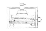
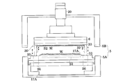
- FIG. 1 It is sectional drawing of a sealing sheet. It is a top view of a sealing sheet. It is a flowchart which shows the sticking process of a sealing sheet. It is a figure which shows conveyance of a sealing sheet. It is a front view which shows the delivery operation
- the sealing sheet T for example, as shown in FIG. 1, a sheet having the same shape as a semiconductor substrate W (hereinafter simply referred to as “substrate W”) is used. Further, the sealing sheet T is provided with a protective first release liner S1 and a second release liner S2 on both surfaces of the sealing layer M.
- the sealing layer M has the same shape to the extent that it can cover the outlines of a plurality of semiconductor element groups formed on the substrate W, as shown in FIG.
- the first release liners S1 and S2 are the same size as the substrate W and have the same shape. Note that the first release liner S1 and the second release liner S2 can be the same shape or rectangle as the substrate W and larger than the size of the substrate W regardless of the shape of the semiconductor element group.
- the sealing layer M is formed into a sheet shape from a sealing material.
- the sealing material include thermosetting silicone resin, epoxy resin, thermosetting polyimide resin, phenol resin, urea resin, melamine resin, unsaturated polyester resin, diallyl phthalate resin, thermosetting urethane resin, and the like.
- a curable resin is mentioned.
- the above-mentioned thermosetting resin and the thermosetting resin composition which contains an additive in an appropriate ratio can also be mentioned.
- Examples of the additive include a filler and a phosphor.
- Examples of the filler include inorganic fine particles such as silica, titania, talc, alumina, aluminum nitride, and silicon nitride, and organic fine particles such as silicone particles.
- the phosphor has a wavelength conversion function, and examples thereof include a yellow phosphor capable of converting blue light into yellow light, and a red phosphor capable of converting blue light into red light. .
- Examples of the yellow phosphor include garnet phosphors such as Y 3 Al 5 O 12 : Ce (YAG (yttrium, aluminum, garnet): Ce).
- Examples of the red phosphor include nitride phosphors such as CaAlSiN 3 : Eu and CaSiN 2 : Eu.
- the sealing layer M is adjusted to a semi-solid state before sealing the semiconductor element. Specifically, when the sealing material contains a thermosetting resin, for example, complete curing (C It is adjusted before being staged, that is, in a semi-cured (B stage) state.
- a thermosetting resin for example, complete curing (C It is adjusted before being staged, that is, in a semi-cured (B stage) state.
- the dimensions of the sealing layer M are appropriately set according to the dimensions of the semiconductor element and the substrate. Specifically, when the sealing sheet is prepared as a long sheet, the length in the left-right direction of the sealing layer M, that is, the width is, for example, 100 mm or more, preferably 200 mm or more. It is 1500 mm or less, preferably 700 mm or less.
- the thickness of the sealing layer M is appropriately set according to the size of the semiconductor element, and is, for example, 30 ⁇ m or more, preferably 100 ⁇ m or more, and, for example, 3000 ⁇ m or less, preferably 1000 ⁇ m or less. .
- first release liner S1 and the second release liner S2 include polymer sheets such as polyethylene sheets, polyester sheets (such as PET), polystyrene sheets, polycarbonate sheets, and polyimide sheets, such as ceramic sheets, such as metal foil. It is done.
- the contact surface in contact with the sealing layer M can be subjected to a release treatment such as a fluorine treatment.
- the dimensions of the first release liner and the second release liner are appropriately set according to the release conditions, and the thickness is, for example, 15 ⁇ m or more, preferably 25 ⁇ m or more, and for example, 125 ⁇ m or less, preferably 75 ⁇ m. It is as follows.
- the transport mechanism 1 and the substrate transport mechanism 2 operate substantially simultaneously.
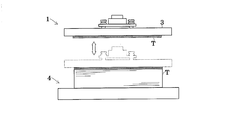
- the transport mechanism 1 moves the suction plate 3 above the sheet supply unit 4. After that, as shown in FIG. 4, the suction plate 3 is lowered to hold the stacked sealing sheets T by suction.
- the suction plate 3 that has moved upward by sucking and holding the sealing sheet T conveys the sealing sheet T to the attaching step (step S1A).
- the sealing sheet T is inverted and turned upward.
- the suction plate 3 moves below the pressing member 6 that moves up and down in the upper housing 5B constituting the decompression chamber 5, and transfers the sealing sheet T to the suction surface of the pressing member 6 (step). S2A).
- the pressing member 6 sucks and holds a region (inactive region) where the sealing layer M of the second release liner S2 of the sealing sheet T is not formed. That is, the inactive region is sucked and held so that an unnecessary external force is not applied to the sealing layer M covering the plurality of semiconductor element groups (active regions) formed on the substrate W.
- the pressing member 6 corresponds to the pressing member of the present invention.
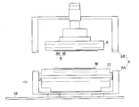
- the affixing roller 11 provided in the peeling unit 10 moves below the pressing member 6.
- the affixing roller 11 rises and a release tape Ts narrower than the encapsulating sheet T is applied to the first release liner S1.
- the peeling unit 10 sticks the peeling tape Ts to the first peeling liner S1 while moving the sticking roller 11, and winds the peeling tape Ts in synchronization with the moving speed.
- the first release liner S1 is peeled off from the sealing sheet T together with the release tape Ts (step S3A).
- the sticking roller 11 returns to the standby position outside the decompression chamber 5.
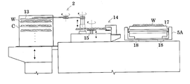
- substrates W accommodated in multiple stages in a cassette C placed on a cassette table that can be raised and lowered are suspended and held by the Bernoulli chuck 13 constituting the substrate transport mechanism 2 in a non-contact manner.
- the Bernoulli chuck 13 transports the substrate W taken out from the cassette C to the aligner 14 and transfers it to the suction pad 15 protruding from the center of the holding surface (step S1B).
- the aligner 14 performs alignment based on notches and the like formed on the substrate W (step S2B). Thereafter, the substrate W is again transported and placed by the Bernoulli chuck 13 from the aligner 14 onto the holding table 17 accommodated in the lower housing 5A (step S3B).
- the holding table 17 moves along the guide rail 18 to the lower side of the pressing member 6 while adsorbing and holding the back surface of the substrate W.
- the upper housing 5B is lowered to a predetermined height toward the lower housing 5A.
- the upper end of the lower housing 5A and the lower end of the upper housing 5B are abutted to form the decompression chamber 5 (step S4).
- the pressure is reduced until the inside of the decompression chamber 5 reaches a vacuum (step S5).
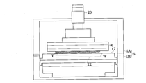
- the pressing member 6 that can be moved up and down by the cylinder 20 in the upper housing 5B is lowered and brought into contact with the sealing sheet T on the substrate W, as shown in FIG.
- the heater 22 provided in the holding table 17 is operated to heat the sealing sheet T (step S6).
- the pressing member 6 is further lowered to a predetermined height to press the sealing sheet T as shown in FIG. Affixing to the surface (step S7).
- the operation of the heater 22 is stopped. Further, the pressing member 6 is raised to release the pressure on the sealing sheet T (step S8). Further, the pressure inside the decompression chamber 5 is gradually increased to return to the atmospheric state.
- step S9 the substrate W on which the sealing sheet T is adhered is held by a transport mechanism such as a robot arm, and the next step. Or is stored in a cassette (step S9). Thus, a series of operations is completed. Thereafter, this series of processes is repeated until the predetermined number of processed sheets is reached (step S10).
- the sealing sheet pasting method described above since the sealing sheet T and the substrate W are kept separated from each other until the decompression chamber 5 reaches a vacuum state, the heat transfer of the holding table 17 is blocked. In addition, softening of the sealing layer M due to the influence of radiant heat from the holding table 17 is suppressed. Therefore, it is possible to avoid bubbles from being caught in the bonding interface between the sealing sheet T and the substrate W before the sealing sheet T is attached to the substrate W. Therefore, even if the main curing process for completely curing the sealing sheet T is performed after the sealing sheet T is pasted, voids are not generated in the sealing layer M and product defects are not caused.
- the present invention can also be implemented in the following forms.
- the outer shape of the second release liner S2 on the side adsorbed by the pressing member 6 out of the first and second release liners S1 and S2 constituting the sealing sheet T is compared with the outer shape of the substrate W. May be set larger.
- the shape may be circular, rectangular or rectangular.
- the case where the first and second release liners S1 and S2 are larger than the substrate W will be described as an example, as shown in FIG.
- the first and second release liners S1 and S2 may be any shape and size that covers the sealing layer M, and may be larger than the substrate W, or the first and second release liners S1 and S2.
- the shape may be different.
- the suction plate 3A of the transport mechanism 1 sucks and holds at least the active area. Therefore, the corners of the second release liner S2 are not sucked and held by the suction plate 3A.
- the sealing sheet T is turned upside down in this state, and moves below the pressing member 6 (step S1A).
- the holding surface of the pressing member 6 is set larger than the shape of the second peeling liner S2.
- the sealing sheet T is clamped by the pressing member 6 and the suction plate 3A (step S2A).
- the holding table 17A that holds the substrate W by suction moves downward.
- the holding member 27 that can be advanced and retracted by an actuator 26 such as a cylinder from a lower position of the step portion 25 formed at the outer peripheral corner of the holding surface of the holding table 17A.
- the four corners of the second peeling liner S2 are clamped by the suction plate 3A and the holding member 27 (step S3A).
- the sandwiched portion is not limited to four locations, and may be four or more locations as long as it is a portion of the second release liner S2 corresponding to the inactive region.
- the transport mechanism 1 releases the suction of the suction plate 3A, returns to the sheet supply unit 4 outside the decompression chamber 5, and prepares to transport the next sealing sheet T.
- the affixing roller 11 shorter than the diameter of the substrate W around which the peeling tape Ts of the peeling unit is wound moves between the sealing sheet T and the substrate W.
- the affixing roller 11 reaches the end of the sealing sheet T
- the affixing roller 11 rises to affix the release tape Ts to the first release liner S1.
- the peeling unit sticks the peeling tape Ts to the first peeling liner S1 while moving the sticking roller 11, and winds the peeling tape Ts in synchronization with the moving speed (step S4A).
- the first release liner S1 is peeled off from the sealing sheet T together with the release tape Ts.
- the sticking roller 11 returns to the standby position outside the decompression chamber 5.
- the upper housing 5B descends to a predetermined height toward the lower housing 5A.
- the holding member 27 is lowered while appropriately pressing the second peeling liner S2.
- the upper and lower ends of the upper and lower housings 5A and 5B are brought into contact with each other to form the decompression chamber 5 (step S5).
- the pressure is reduced until the inside of the decompression chamber 5 reaches a vacuum (step S6).
- the pressing member 6 that can be moved up and down by the cylinder 20 in the upper housing 5B is lowered and brought into contact with the sealing sheet T on the substrate W.
- the sealing sheet T is heated by the heater 22 (step S7), and as the sealing sheet T starts to soften, the pressing member 6 is further lowered to a predetermined height as shown in FIG. T is pressed and the sealing sheet T is affixed on the surface of the board
- the operation of the heater 22 is stopped. Further, the pressing member 6 is raised to release the pressurization of the sealing sheet T and the clamping of the second release liner S2 (step S9). At this time, the holding member 27 is stored in the step portion 25 of the holding table 17A. The pressure inside the decompression chamber 5 is gradually increased to return to the atmospheric state.
- step S10 the substrate W to which the sealing sheet T is attached is transferred to a transport mechanism such as a robot arm. And is carried to the next process or stored in a cassette. Thereafter, this series of processes is repeated until the predetermined number of processed sheets is reached (step S12).
- the gripping unit 30 or the support unit 31 may be moved horizontally to apply an appropriate tension to the second peeling liner S2.
- the pressing member 6 may have a heater. However, after the heater is turned off, it is preferable that the pressing member 6 is cooled by a Peltier element, a heat sink, or the like so that the pressing member 6 immediately decreases to room temperature.
- the substrate shape may be a square, a rectangle, or a polygon.
- the transport mechanism for transporting the substrate W may use a robot arm having a horseshoe-shaped tip and a suction function.
- the robot arm When using the robot arm, the back surface of the substrate W may be sucked and held by the robot arm and transferred.
- the holding table 17 includes a suction pad that moves out of the center of the holding surface, and may be configured to receive the substrate W with the suction pad.
- the holding of the sealing sheet T by the pressing member 6 is not limited to the above method, and may be held by an electrostatic chuck.
- the present invention is suitable for attaching a sealing sheet to a semiconductor substrate efficiently and accurately.
Landscapes
- Encapsulation Of And Coatings For Semiconductor Or Solid State Devices (AREA)
Abstract
封止シートは、第1および第2剥離ライナの添設された半導体基板の形状以上の大きさを有する封止シートの当該第2剥離ライナの面を減圧室内に備えられた押圧部材によって保持し、第1剥離ライナを剥離し、ヒータの埋設された保持テーブルに半導体基板を載置し、半導体基板と封止シートを対向させる。減圧室内を減圧して真空状態した後に、減圧室内でヒータによって封止シートを加熱しながら押圧部材で加圧して半導体基板に封止シートを貼り付ける。
Description
本発明は、半導体装置を製造する過程で、回路基板を含む半導体基板の回路面に樹脂組成物からなる封止層の形成された封止シートを貼り付け、当該回路面を封止する封止シート貼付け方法に関する。
1個の半導体チップの周りを枠体で囲んだ後に、樹脂を含浸させたプリプレグから成る第1の封止用樹脂シートと第2の封止用樹脂シートによって当該半導体チップの両面をそれぞれから挟み込み、半導体チップを封止して半導体装置を製造している(特許文献1を参照)。
しかしながら、上記従来方法では次のような問題が生じている。
すなわち、近年、アプリケーションの急速な進歩に伴う高密度実装の要求により、半導体装置が小型化される傾向にある。したがって、ダイシング処理によって半導体ウエハを半導体素子に分断した後に、半導体素子を個々に樹脂で封止しているので、スループットが低下し、ひいては生産効率を低下させるといった不都合が生じている。
本発明はこのような事情に鑑みてなされたものであって、半導体基板に封止シートを効率よく、かつ、精度よく貼り付けることのできる封止シート貼付け方法を提供することを主たる目的とする。
そこで、本発明者たちは、当該不都合を解決するために、実験やシミュレーションを繰り返して鋭意検討した結果、以下の知見を得た。
半導体基板の全面に樹脂組成物からなる封止層の形成された枚葉の封止シートを貼り付けて硬化させた後に、当該半導体装置に分断することを試みた。
しかしながら、ダイシング処理によって分断されたチップに比べて大面積の半導体基板と同形状の封止シートを当該半導体基板に貼り付ける当該方法の場合、封止シート自体が厚みおよび剛性を有している。その結果、貼付け過程で封止シートと半導体基板との接着界面に気泡が巻き込まれやすく、封止層内にボイドが発生する。特に、封止シートを貼り付けた後に、加熱よって封止層の重合反応を促進させて本硬化させる場合、気泡が膨張して半導体装置が不良品になるといった問題が新たに発生した。
また、減圧室内を真空状態にして封止シートを半導体基板に加熱しながら貼り付けたにも関わらず、接着界面に気泡が巻き込まれていた。
当該原因を究明すべく実験を繰り返した結果、貼付け処理を連続的に繰り返した場合に頻繁に生じることが判明した。すなわち、保持テーブル上の半導体基板に樹脂シートを載置したまま減圧室の減圧を開始すると、室内が真空状態に達するまでに保持テーブルの余熱または輻射熱の影響で封止層が軟化して気泡を巻き込むことが分かった。
この発明は、このような目的を達成するために、次のような構成をとる。
すなわち、半導体装置を製造する過程で樹脂組成物からなる封止層の形成された封止シートを半導体基板に貼り付ける封止シート貼付け方法であって、
前記封止シートは、剥離ライナの添設された半導体基板の形状以上の大きさを有し、
減圧室内に備えられた加圧部材によって封止シートの剥離ライナの面を保持するとともに、ヒータの埋設された保持テーブルに半導体基板を載置し、半導体基板と封止シートを対向させる載置過程と、
前記減圧室内を減圧して真空状態する減圧過程と、
真空状態の前記減圧室内でヒータによって封止シートを加熱しながら加圧部材で加圧して半導体基板に貼り付ける貼付け過程と、
を備えたことを特徴とする。
前記封止シートは、剥離ライナの添設された半導体基板の形状以上の大きさを有し、
減圧室内に備えられた加圧部材によって封止シートの剥離ライナの面を保持するとともに、ヒータの埋設された保持テーブルに半導体基板を載置し、半導体基板と封止シートを対向させる載置過程と、
前記減圧室内を減圧して真空状態する減圧過程と、
真空状態の前記減圧室内でヒータによって封止シートを加熱しながら加圧部材で加圧して半導体基板に貼り付ける貼付け過程と、
を備えたことを特徴とする。
上記方法によれば、減圧室内が真空状態に達するまで、半導体基板と封止シートが対向している。すなわち、半導体基板と封止シートは、非接触状態が保たれている。したがって、真空状態に達するまでに封止層が保持テーブルの熱によって軟化するのを抑制させるとともに、半導体基板に封止シートが接触するのを回避させる。その結果、封止シートと半導体基板の接着界面からエアーが完全に排出されるので、当該接着界面に気泡が巻き込まれるのを回避することができ、ひいては半導体装置の不良率を低減させることができる。
なお、上記方法において、圧部材は、ヒータを備え、
貼付け過程は、保持テーブルと加圧部材によって封止シートを加熱させてもよい。
貼付け過程は、保持テーブルと加圧部材によって封止シートを加熱させてもよい。
この方法によれば、加熱部材と保持テーブルとによって挟み込まれた封止シートに熱を効率よく伝達させることができる。
また、上記方法において、封止シートの保持は、次のように実施してもよい。
例えば、封止シートの封止層は、半導体基板に形成された複数個の半導体素子群を被覆するよう当該半導体素子群の輪郭と同形状をしており、
剥離ライナは、半導体基板の外形以上の大きさを有し、
載置過程では、封止層の外側の領域の剥離ライナを保持する。
例えば、封止シートの封止層は、半導体基板に形成された複数個の半導体素子群を被覆するよう当該半導体素子群の輪郭と同形状をしており、
剥離ライナは、半導体基板の外形以上の大きさを有し、
載置過程では、封止層の外側の領域の剥離ライナを保持する。
この方法によれば、封止シートを保持するときの外力が当該封止シートの剥離ライナ上に形成された封止層にかかるのを回避し、封止層の変形を抑制することができる。また、剥離ライナが半導体基板の外形より大きい場合に封止シートを好適に保持することができる。例えば、封止シートの外周の複数箇所をニップし、外側に引っ張ることにより、封止シートに適度のテンションを付与することができる。
本発明の封止シート貼付け方法によれば、封止シートを半導体基板に精度よく貼り付けることができる。
5 … 減圧室
6 … 押圧部材
10 … 剥離ユニット
17 … 保持テーブル
22 … ヒータ
26 … アクチュエータ
27 … 保持部材
T … 封止シート
M … 封止層
S1 … 第1剥離ライナ
S2 … 第2剥離ライナ
W … 半導体基板
6 … 押圧部材
10 … 剥離ユニット
17 … 保持テーブル
22 … ヒータ
26 … アクチュエータ
27 … 保持部材
T … 封止シート
M … 封止層
S1 … 第1剥離ライナ
S2 … 第2剥離ライナ
W … 半導体基板
以下、図面を参照して本発明の一実施例を説明する。表面に複数個の半導体素子が形成された半導体基板に、樹脂組成物からなる封止層の形成された封止シートを貼り付ける場合を例に取って説明する。
<封止シート>
封止シートTは、例えば、図1に示すように、半導体基板W(以下、単に「基板W」という)と同形状のもが利用される。また、当該封止シートTは、封止層Mの両面に保護用の第1剥離ライナS1および第2剥離ライナS2が添設されている。本実施例では、封止層Mは、図2に示すように、基板Wに形成された複数個の半導体素子群の輪郭を被覆できる程度で同形状をしている。また、第1剥離ライナS1およびS2は、基板Wと同じ大きさで、かつ、同じ形状をしている。なお、第1剥離ライナS1および第2剥離ライナS2は、半導体素子群の形状に関わらず、基板Wと同形状または矩形で、かつ、基板Wのサイズ以上のものを利用することができる。
封止シートTは、例えば、図1に示すように、半導体基板W(以下、単に「基板W」という)と同形状のもが利用される。また、当該封止シートTは、封止層Mの両面に保護用の第1剥離ライナS1および第2剥離ライナS2が添設されている。本実施例では、封止層Mは、図2に示すように、基板Wに形成された複数個の半導体素子群の輪郭を被覆できる程度で同形状をしている。また、第1剥離ライナS1およびS2は、基板Wと同じ大きさで、かつ、同じ形状をしている。なお、第1剥離ライナS1および第2剥離ライナS2は、半導体素子群の形状に関わらず、基板Wと同形状または矩形で、かつ、基板Wのサイズ以上のものを利用することができる。
封止層Mは、封止材料からシート形状に形成されている。封止材料としては、例えば、熱硬化性シリコーン樹脂、エポキシ樹脂、熱硬化性ポリイミド樹脂、フェノール樹脂、ユリア樹脂、メラミン樹脂、不飽和ポリエステル樹脂、ジアリルフタレート樹脂、熱硬化性ウレタン樹脂、などの熱硬化性樹脂が挙げられる。また、封止材料として、上記した熱硬化性樹脂と、添加剤を適宜の割合で含有する熱硬化性樹脂組成物を挙げることもできる。
添加剤としては、例えば、充填剤、蛍光体などが挙げられる。充填剤としては、例えば、シリカ、チタニア、タルク、アルミナ、窒化アルミニウム、窒化ケイ素などの無機微粒子、例えば、シリコーン粒子、などの有機微粒子などが挙げられる。蛍光体は、波長変換機能を有しており、例えば、青色光を黄色光に変換することのできる黄色蛍光体、青色光を赤色光に変化することのできる赤色蛍光体などを挙げることができる。黄色蛍光体としては、例えば、Y3Al5O12:Ce(YAG(イットリウム・アルミニウム・ガーネット):Ce)などのガーネット型蛍光体が挙げられる。赤色蛍光体としては、例えば、CaAlSiN3:Eu、CaSiN2:Euなどの窒化物蛍光体などが挙げられる。
封止層Mは、半導体素子を封止する前において、半固形状に調整されており、具体的には、封止材料が熱硬化性樹脂を含有する場合には、例えば、完全硬化(Cステージ化)する前、つまり、半硬化(Bステージ)状態で調整されている。
封止層Mの寸法は、半導体素子および基板の寸法に応じて適宜に設定されている。具体的には、封止シートが長尺のシートとして用意される場合における封止層Mの左右方向における長さ、つまり、幅は、例えば、100mm以上、好ましくは、200mm以上であり、例えば、1500mm以下、好ましくは、700mm以下である。また、封止層Mの厚みは、半導体素子に寸法に対応して適宜に設定され、例えば、30μm以上、好ましくは、100μm以上であり、また、例えば、3000μm以下、好ましくは、1000μm以下である。
第1剥離ライナS1および第2剥離ライナS2は、例えば、ポリエチレンシート、ポリエステルシート(PETなど)、ポリスチレンシート、ポリカーボネートシート、ポリイミドシートなどのポリマーシート、例えば、セラミックシート、例えば、金属箔などが挙げられる。剥離ライナにおいて、封止層Mと接触する接触面には、フッ素処理などの離型処理を施すこともできる。第1剥離ライナおよび第2剥離ライナの寸法は、剥離条件に応じて適宜に設定され、厚みが、例えば、15μm以上、好ましくは、25μm以上であり、また、例えば、125μm以下、好ましくは、75μm以下である。
<封止シート貼付け方法>
封止シートを基板に貼り付ける一巡の動作を図3のフローチャートおよび図4から図10に基づいて説明する。
封止シートを基板に貼り付ける一巡の動作を図3のフローチャートおよび図4から図10に基づいて説明する。
貼付け指令が出されると、搬送機構1および基板搬送機構2が略同時に作動する。
搬送機構1は、吸着プレート3をシート供給部4の上方へ移動させる。その後、図4に示すように、吸着プレート3を下降させて積層されている封止シートTを吸着保持する。
封止シートTを吸着保持して上方に移動した吸着プレート3は、貼付け工程へと封止シートTを搬送する(ステップS1A)。この搬送過程で、封止シートTを反転させて上向きにする。図5に示すように、減圧室5を構成する上ハウジング5B内で昇降する押圧部材6の下方に吸着プレート3が移動し、封止シートTを押圧部材6の吸着面へと受け渡す(ステップS2A)。このとき、押圧部材6は、封止シートTの第2剥離ライナS2の封止層Mの形成されていない領域(非アクティブ領域)を吸着保持する。すなわち、基板Wに形成された複数個の半導体素子群(アクティブ領域)を被覆する封止層Mに不要な外力がかからないように、非アクティブ領域を吸着保持する。なお、押圧部材6は、本発明の加圧部材に相当する。
図6に示すように、剥離ユニット10に備わった貼付けローラ11が、押圧部材6の下方へと移動する。封止シートTの端部に貼付けローラ11が達すると上昇し、封止シートTよりも幅の狭い剥離テープTsを第1剥離ライナS1に貼り付ける。その後、剥離ユニット10は、貼付けローラ11を移動させながら剥離テープTsを第1剥離ライナS1に貼り付けるとともに、当該移動速度に同期させて剥離テープTsを巻き取る。このとき、第1剥離ライナS1は、剥離テープTsと一体となって封止シートTから剥離される(ステップS3A)。第1剥離ライナS1の剥離が完了すると、貼付けローラ11は、減圧室5の外側の待機位置へと戻る。
他方、昇降可能なカセット台に載置されたカセットCに所定間隔をおいて多段に収納されている基板Wが、基板搬送機構2を構成するベルヌーイチャック13によって表面を非接触で懸垂保持される。ベルヌーイチャック13は、図7に示すように、カセットCから取り出した基板Wをアライナ14へと搬送し、保持面中央から突出する吸着パッド15に受け渡す(ステップS1B)。
アライナ14は、基板Wに形成されたノッチなどに基づいて位置合わせをする(ステップS2B)。その後、基板Wは、再度ベルヌーイチャック13によってアライナ14から下ハウジング5Aに収納されている保持テーブル17に搬送および載置される(ステップS3B)。
保持テーブル17は、図8に示すように、基板Wの裏面を吸着保持したまま、ガイドレール18に沿って押圧部材6の下方へと移動する。押圧部材6と保持テーブル17とが対向する位置合わせが完了すると、上ハウジング5Bが、下ハウジング5Aに向けて所定高さまで下降する。下ハウジング5Aの上端と上ハウジング5Bの下端とが突き合わされて減圧室5が形成される(ステップS4)。その後、減圧室5の内部が真空に達するまで減圧してゆく(ステップS5)。
減圧室5の内部が真空状態に達すると、図9に示すように、上ハウジング5B内でシリンダ20によって昇降可能な押圧部材6を下降させて基板Wに封止シートTに当接させる。このとき、保持テーブル17に備わったヒータ22を作動させて封止シートTを加熱する(ステップS6)。加熱により封止シートTが軟化を開始するのに伴って、図10に示すように、さらに押圧部材6を所定高さまで下降させて封止シートTを押圧し、封止シートTを基板Wの表面に貼り付ける(ステップS7)。
加熱および加圧処理が所定時間に達すると、ヒータ22の作動を停止させる。また、押圧部材6を上昇させて封止シートTの加圧を解除する(ステップS8)。さらに、減圧室5の内部の気圧を徐々に上げて大気状態に戻す。
その後、減圧室5の内部が大気状態に達した時点で、上ハウジング5Bを上昇させた後に、封止シートTの貼り付けられた基板Wをロボットアームなどの搬送機構によって保持して次の工程に搬送またはカセットに収納する(ステップS9)。以上で一連の動作が終了する。その後、所定の処理枚数に達するまで、この一連の処理が繰り返される(ステップS10)。
上述の封止シート貼付け方法によれば、減圧室5が真空状態に達するまで、封止シートTと基板Wが、互いに離間した状態を保っているので、保持テーブル17の熱の伝達が遮断されるとともに、保持テーブル17からの輻射熱の影響で封止層Mが軟化するのを抑制される。したがって、封止シートTを基板Wに貼り付けるまでに、封止シートTと基板Wの接着界面に気泡が巻き込まれるのを回避することができる。したがって、封止シートTを貼り付けた後に、封止シートTを完全に硬化させる本硬化処理を行っても、封止層Mにボイドが発生して製品不良を招くことがない。
なお、本発明は以下のような形態で実施することもできる。
(1)上記各実施例において、封止シートTを構成する第1、第2剥離ライナS1、S2のうち押圧部材6よって吸着される側の第2剥離ライナS2の外形を基板Wの外形よりも大きく設定してもよい。その形状は、円形、矩形または長方形であってもよい。当該変形例において、図11に示すように、第1、第2剥離ライナS1、S2は、基板Wよりも大きい矩形である場合を例にとって説明する。なお、第1、第2剥離ライナS1、S2は、封止層Mを被覆する形状および大きさであればよく、基板Wよりも大きくてもよいし、第1、第2剥離ライナS1、S2の形状は、異なる形状であってもよい。
次に、当該封止シートTを基板Wに貼り付ける一巡の動作について、図12に示すフローチャートおよび図13から図18に基づいて説明する。なお、上記実施例と同一の処理については、説明を省略し、異なる動作の処理について説明する。したがって、基板Wの搬出から押圧部材6との対向位置合わせまでの説明については省略する。
搬送機構1の吸着プレート3Aは、少なくともアクティブ領域を吸着保持する。したがって、第2剥離ライナS2の角部は、吸着プレート3Aによって吸着保持されていない。封止シートTは、この状態で上下反転させられ、押圧部材6の下方に移動する(ステップS1A)。
押圧部材6の保持面は、第2剥離ライナS2の形状よりも大きく設定されている。図13に示すように、押圧部材6と吸着プレート3Aによって封止シートTを挟持する(ステップS2A)。この状態で、基板Wを吸着保持した保持テーブル17Aが、下方へと移動してくる。押圧部材6と保持テーブル17Aとが対向する位置合わせが完了すると、保持テーブル17Aの保持面の外周角部に形成された段部25の低い位置からシリンダなどのアクチュエータ26によって進退可能な保持部材27が上昇する。すなわち、吸着プレート3Aと保持部材27によって第2剥離ライナS2の4箇所の角部が挟持される(ステップS3A)。なお、挟持する部分は4箇所に限定されず、非アクティブ領域に相当する第2剥離ライナS2の部分であれば4箇所以上であってもよい。
搬送機構1は、吸着プレート3Aの吸着を解除して減圧室5の外側のシート供給部4へと戻り、次の封止シートTの搬送の準備をする。
次に、図15に示すように、剥離ユニットの剥離テープTsを巻きかけた基板Wの直径よりも短い貼付けローラ11が、封止シートTと基板Wの間に移動する。封止シートTの端部に貼付けローラ11が達すると、貼付けローラ11が上昇して剥離テープTsを第1剥離ライナS1に貼り付ける。その後、剥離ユニットは、貼付けローラ11を移動させながら剥離テープTsを第1剥離ライナS1に貼り付けるとともに、当該移動速度に同期させて剥離テープTsを巻き取る(ステップS4A)。このとき、第1剥離ライナS1は、剥離テープTsと一体となって封止シートTから剥離される。第1剥離ライナS1の剥離が完了すると、貼付けローラ11は、減圧室5の外側の待機位置へと戻る。
図16に示すように、上ハウジング5Bが、下ハウジング5Aに向けて所定高さまで下降する。このとき、上ハウジング5Bの下降に同期して保持部材27が、第2剥離ライナS2に適度に押圧を付与しながら下降する。上下ハウジング5A、5Bの上端と下端とが突き合わされて減圧室5が形成される(ステップS5)。その後、減圧室5の内部が真空に達するまで減圧されてゆく(ステップS6)。
減圧室5の内部が真空状態に達すると、図17に示すように、上ハウジング5B内でシリンダ20によって昇降可能な押圧部材6を下降させて基板Wに封止シートTに当接させる。ヒータ22によって封止シートTを加熱し(ステップS7)、封止シートTが軟化を開始するのに伴って、図18に示すように、さらに押圧部材6を所定高さまで下降させて封止シートTを押圧し、封止シートTを基板Wの表面に貼り付ける(ステップS8)。
加熱および加圧処理が所定時間に達すると、ヒータ22の作動を停止させる。また、押圧部材6を上昇させて封止シートTの加圧および第2剥離ライナS2の挟持を解除する(ステップS9)。このとき、保持部材27は、保持テーブ17Aの段部25に収納される。減圧室5の内部の気圧を徐々に上げて大気状態に戻す。
その後、上記実施例と同様に、減圧室5の内部が大気状態に達した時点で、上ハウジング5Bを上昇させた後に、封止シートTの貼り付けられた基板Wをロボットアームなどの搬送機構によって保持して次の工程に搬送またはカセットに収納する(ステップS10)。その後、所定の処理枚数に達するまで、この一連の処理が繰り返される(ステップS12)
なお、当該変形例において、第2剥離ライナS2の角部を、図19および図20に示すように、保持部材27に換えて把持部30で把持してもよい。すなわち、進退する支持部31の先端に、可動片32と固定片33を備え、当該可動片32を昇降させて第2剥離ライナS2の角部の把持または解除を行う。なお、支持部31は、保持テーブル17Aの段部において進退する。
さらに、把持部30または支持部31を水平移動させて第2剥離ライナS2に適度のテンションを付与するように構成してもよい。
(2)上記各実施例において、押圧部材6にヒータを備えた構成であってもよい。ただし、当該ヒータをオフにした後に、押圧部材6が、即時に室温まで低下するようペルチェ素子やヒートシンクなどによって冷却することが好ましい。
(3)上記実施例では、円形の基板Wを例にとって説明したが、基板形状は、正方形、長方形または多角形であってもよい。
(4)上記実施例において、基板Wを搬送する搬送機構は、先端が馬蹄形で吸着機能を有するロボットアームを利用してもよい。ロボットアームを利用する場合、基板Wの裏面をロボットアームで吸着保持して搬送すればよい。また、保持テーブル17は、アライナ14と同様に、保持面の中央から出退する吸着パッドを備え、当該吸着パッドで基板Wを受け取るように構成すればよい。
(5)上記各実施例において、押圧部材6による封止シートTの保持は、上記方法に限定されず、静電チャックによって保持してもよい。
以上のように、本発明は、半導体基板に封止シートを効率よく、かつ、精度よく貼り付けるのに適している。
Claims (3)
- 半導体装置を製造する過程で樹脂組成物からなる封止層の形成された封止シートを半導体基板に貼り付ける封止シート貼付け方法であって、
前記封止シートは、剥離ライナの添設された半導体基板の形状以上の大きさを有し、
減圧室内に備えられた加圧部材によって封止シートの剥離ライナ面を保持するとともに、ヒータの埋設された保持テーブルに半導体基板を載置し、半導体基板と封止シートを対向させる載置過程と、
前記減圧室内を減圧して真空状態する減圧過程と、
真空状態の前記減圧室内でヒータによって封止シートを加熱しながら加圧部材で加圧して半導体基板に貼り付ける貼付け過程と、
を備えたことを特徴とする封止シート貼付け方法。 - 請求項1に記載の封止シート貼付け方法において、
前記加圧部材は、ヒータを備え、
前記貼付け過程は、保持テーブルと加圧部材によって封止シートを加熱させる
ことを特徴とする封止シート貼付け方法。 - 請求項1または請求項2に記載の封止シート貼付け方法において、
前記封止シートの封止層は、半導体基板に形成された複数個の半導体素子群を被覆するよう当該半導体素子群の輪郭と同形状をしており、
前記剥離ライナは、半導体基板の外形以上の大きさを有し、
前記載置過程では、封止層の外側の領域の剥離ライナを保持する
ことを特徴とする封止シート貼付け方法。
Applications Claiming Priority (2)
| Application Number | Priority Date | Filing Date | Title |
|---|---|---|---|
| JP2013254045A JP2015115347A (ja) | 2013-12-09 | 2013-12-09 | 封止シート貼付け方法 |
| JP2013-254045 | 2013-12-09 |
Publications (1)
| Publication Number | Publication Date |
|---|---|
| WO2015087763A1 true WO2015087763A1 (ja) | 2015-06-18 |
Family
ID=53371071
Family Applications (1)
| Application Number | Title | Priority Date | Filing Date |
|---|---|---|---|
| PCT/JP2014/082048 Ceased WO2015087763A1 (ja) | 2013-12-09 | 2014-12-03 | 封止シート貼付け方法 |
Country Status (3)
| Country | Link |
|---|---|
| JP (1) | JP2015115347A (ja) |
| TW (1) | TW201533784A (ja) |
| WO (1) | WO2015087763A1 (ja) |
Cited By (1)
| Publication number | Priority date | Publication date | Assignee | Title |
|---|---|---|---|---|
| EP3540765A4 (en) * | 2016-11-11 | 2020-05-13 | SHIN-ETSU ENGINEERING Co., Ltd. | RESIN SEALING DEVICE AND RESIN SEALING METHOD |
Families Citing this family (1)
| Publication number | Priority date | Publication date | Assignee | Title |
|---|---|---|---|---|
| CN116888714A (zh) * | 2021-02-01 | 2023-10-13 | 长濑化成株式会社 | 电子部件安装基板的密封方法及热固化性片材 |
Citations (5)
| Publication number | Priority date | Publication date | Assignee | Title |
|---|---|---|---|---|
| WO2008142934A1 (ja) * | 2007-05-15 | 2008-11-27 | Lintec Corporation | シート貼付装置及び貼付方法 |
| JP2009272975A (ja) * | 2008-05-09 | 2009-11-19 | Nippon Dempa Kogyo Co Ltd | 圧電部品の製造方法 |
| JP2010109246A (ja) * | 2008-10-31 | 2010-05-13 | Yaskawa Electric Corp | 半導体装置および半導体装置の製造方法 |
| JP2010179507A (ja) * | 2009-02-04 | 2010-08-19 | Apic Yamada Corp | 圧縮成形方法 |
| WO2012023373A1 (ja) * | 2010-08-20 | 2012-02-23 | ニチゴー・モートン株式会社 | 積層装置 |
-
2013
- 2013-12-09 JP JP2013254045A patent/JP2015115347A/ja active Pending
-
2014
- 2014-12-03 WO PCT/JP2014/082048 patent/WO2015087763A1/ja not_active Ceased
- 2014-12-08 TW TW103142532A patent/TW201533784A/zh unknown
Patent Citations (5)
| Publication number | Priority date | Publication date | Assignee | Title |
|---|---|---|---|---|
| WO2008142934A1 (ja) * | 2007-05-15 | 2008-11-27 | Lintec Corporation | シート貼付装置及び貼付方法 |
| JP2009272975A (ja) * | 2008-05-09 | 2009-11-19 | Nippon Dempa Kogyo Co Ltd | 圧電部品の製造方法 |
| JP2010109246A (ja) * | 2008-10-31 | 2010-05-13 | Yaskawa Electric Corp | 半導体装置および半導体装置の製造方法 |
| JP2010179507A (ja) * | 2009-02-04 | 2010-08-19 | Apic Yamada Corp | 圧縮成形方法 |
| WO2012023373A1 (ja) * | 2010-08-20 | 2012-02-23 | ニチゴー・モートン株式会社 | 積層装置 |
Cited By (1)
| Publication number | Priority date | Publication date | Assignee | Title |
|---|---|---|---|---|
| EP3540765A4 (en) * | 2016-11-11 | 2020-05-13 | SHIN-ETSU ENGINEERING Co., Ltd. | RESIN SEALING DEVICE AND RESIN SEALING METHOD |
Also Published As
| Publication number | Publication date |
|---|---|
| TW201533784A (zh) | 2015-09-01 |
| JP2015115347A (ja) | 2015-06-22 |
Similar Documents
| Publication | Publication Date | Title |
|---|---|---|
| US11018112B2 (en) | Bonding method of semiconductor chip and bonding apparatus of semiconductor chip | |
| JP5334135B2 (ja) | 積層装置 | |
| KR102759515B1 (ko) | 웨이퍼의 가공 방법 | |
| KR102050541B1 (ko) | 초박막 웨이퍼의 임시 본딩을 위한 방법 및 장치 | |
| TWI745532B (zh) | 半導體基板之處理方法及處理裝置 | |
| KR101617316B1 (ko) | 디바이스 웨이퍼와 캐리어 웨이퍼의 본딩/디본딩 방법 및 본딩/디본딩 장치 | |
| CN106057718B (zh) | 被加工物的切削加工方法 | |
| WO2014167947A1 (ja) | 半導体装置の製造方法 | |
| JP4945339B2 (ja) | 半導体集積回路装置の製造方法 | |
| WO2014167948A1 (ja) | 封止シート貼付け方法および封止シート貼付け装置 | |
| WO2015087763A1 (ja) | 封止シート貼付け方法 | |
| JP6616457B2 (ja) | チップの接合方法及びチップの接合装置 | |
| TW201501253A (zh) | 密封片貼附方法及密封片貼附裝置 | |
| JP2005175207A (ja) | 半導体装置の製造方法、研削用補強部材、及びその貼り付け方法 | |
| WO2015087762A1 (ja) | 封止シート貼付け方法 | |
| JP2015119040A (ja) | 封止シート貼付け方法 | |
| JP4926630B2 (ja) | 固体撮像装置の製造方法および製造装置、並びに貼付装置 | |
| JP2012115911A (ja) | 基板の研削方法およびそれを用いて作製された半導体素子 | |
| JP2024106774A (ja) | 保護シート配設方法および保護シート | |
| JP2015115348A (ja) | 封止シート貼付け方法 | |
| KR20210127083A (ko) | 판상물의 가공 방법 | |
| JP2012156517A (ja) | 半導体集積回路装置の製造方法 | |
| WO2014178268A1 (ja) | 封止シート貼付け方法および封止シート貼付け装置 | |
| JP2009187969A (ja) | 基板の加工方法 |
Legal Events
| Date | Code | Title | Description |
|---|---|---|---|
| 121 | Ep: the epo has been informed by wipo that ep was designated in this application |
Ref document number: 14869457 Country of ref document: EP Kind code of ref document: A1 |
|
| NENP | Non-entry into the national phase |
Ref country code: DE |
|
| 122 | Ep: pct application non-entry in european phase |
Ref document number: 14869457 Country of ref document: EP Kind code of ref document: A1 |