WO2015083532A1 - 光半導体装置用エポキシ樹脂組成物およびそれを用いて得られる光半導体装置用リードフレーム、封止型光半導体素子ならびに光半導体装置 - Google Patents
光半導体装置用エポキシ樹脂組成物およびそれを用いて得られる光半導体装置用リードフレーム、封止型光半導体素子ならびに光半導体装置 Download PDFInfo
- Publication number
- WO2015083532A1 WO2015083532A1 PCT/JP2014/080410 JP2014080410W WO2015083532A1 WO 2015083532 A1 WO2015083532 A1 WO 2015083532A1 JP 2014080410 W JP2014080410 W JP 2014080410W WO 2015083532 A1 WO2015083532 A1 WO 2015083532A1
- Authority
- WO
- WIPO (PCT)
- Prior art keywords
- optical semiconductor
- semiconductor device
- epoxy resin
- resin composition
- reflector
- Prior art date
- Legal status (The legal status is an assumption and is not a legal conclusion. Google has not performed a legal analysis and makes no representation as to the accuracy of the status listed.)
- Ceased
Links
Images



Classifications
-
- H—ELECTRICITY
- H10—SEMICONDUCTOR DEVICES; ELECTRIC SOLID-STATE DEVICES NOT OTHERWISE PROVIDED FOR
- H10H—INORGANIC LIGHT-EMITTING SEMICONDUCTOR DEVICES HAVING POTENTIAL BARRIERS
- H10H20/00—Individual inorganic light-emitting semiconductor devices having potential barriers, e.g. light-emitting diodes [LED]
- H10H20/80—Constructional details
- H10H20/85—Packages
- H10H20/852—Encapsulations
- H10H20/854—Encapsulations characterised by their material, e.g. epoxy or silicone resins
-
- C—CHEMISTRY; METALLURGY
- C08—ORGANIC MACROMOLECULAR COMPOUNDS; THEIR PREPARATION OR CHEMICAL WORKING-UP; COMPOSITIONS BASED THEREON
- C08G—MACROMOLECULAR COMPOUNDS OBTAINED OTHERWISE THAN BY REACTIONS ONLY INVOLVING UNSATURATED CARBON-TO-CARBON BONDS
- C08G59/00—Polycondensates containing more than one epoxy group per molecule; Macromolecules obtained by polymerising compounds containing more than one epoxy group per molecule using curing agents or catalysts which react with the epoxy groups
- C08G59/18—Macromolecules obtained by polymerising compounds containing more than one epoxy group per molecule using curing agents or catalysts which react with the epoxy groups ; e.g. general methods of curing
- C08G59/20—Macromolecules obtained by polymerising compounds containing more than one epoxy group per molecule using curing agents or catalysts which react with the epoxy groups ; e.g. general methods of curing characterised by the epoxy compounds used
- C08G59/22—Di-epoxy compounds
- C08G59/24—Di-epoxy compounds carbocyclic
- C08G59/245—Di-epoxy compounds carbocyclic aromatic
-
- C—CHEMISTRY; METALLURGY
- C08—ORGANIC MACROMOLECULAR COMPOUNDS; THEIR PREPARATION OR CHEMICAL WORKING-UP; COMPOSITIONS BASED THEREON
- C08G—MACROMOLECULAR COMPOUNDS OBTAINED OTHERWISE THAN BY REACTIONS ONLY INVOLVING UNSATURATED CARBON-TO-CARBON BONDS
- C08G59/00—Polycondensates containing more than one epoxy group per molecule; Macromolecules obtained by polymerising compounds containing more than one epoxy group per molecule using curing agents or catalysts which react with the epoxy groups
- C08G59/18—Macromolecules obtained by polymerising compounds containing more than one epoxy group per molecule using curing agents or catalysts which react with the epoxy groups ; e.g. general methods of curing
- C08G59/40—Macromolecules obtained by polymerising compounds containing more than one epoxy group per molecule using curing agents or catalysts which react with the epoxy groups ; e.g. general methods of curing characterised by the curing agents used
- C08G59/42—Polycarboxylic acids; Anhydrides, halides or low molecular weight esters thereof
-
- C—CHEMISTRY; METALLURGY
- C08—ORGANIC MACROMOLECULAR COMPOUNDS; THEIR PREPARATION OR CHEMICAL WORKING-UP; COMPOSITIONS BASED THEREON
- C08K—Use of inorganic or non-macromolecular organic substances as compounding ingredients
- C08K3/00—Use of inorganic substances as compounding ingredients
- C08K3/01—Use of inorganic substances as compounding ingredients characterized by their specific function
- C08K3/013—Fillers, pigments or reinforcing additives
-
- C—CHEMISTRY; METALLURGY
- C08—ORGANIC MACROMOLECULAR COMPOUNDS; THEIR PREPARATION OR CHEMICAL WORKING-UP; COMPOSITIONS BASED THEREON
- C08K—Use of inorganic or non-macromolecular organic substances as compounding ingredients
- C08K3/00—Use of inorganic substances as compounding ingredients
- C08K3/18—Oxygen-containing compounds, e.g. metal carbonyls
- C08K3/20—Oxides; Hydroxides
- C08K3/22—Oxides; Hydroxides of metals
-
- C—CHEMISTRY; METALLURGY
- C08—ORGANIC MACROMOLECULAR COMPOUNDS; THEIR PREPARATION OR CHEMICAL WORKING-UP; COMPOSITIONS BASED THEREON
- C08K—Use of inorganic or non-macromolecular organic substances as compounding ingredients
- C08K5/00—Use of organic ingredients
- C08K5/54—Silicon-containing compounds
- C08K5/541—Silicon-containing compounds containing oxygen
- C08K5/5415—Silicon-containing compounds containing oxygen containing at least one Si—O bond
- C08K5/5419—Silicon-containing compounds containing oxygen containing at least one Si—O bond containing at least one Si—C bond
-
- C—CHEMISTRY; METALLURGY
- C08—ORGANIC MACROMOLECULAR COMPOUNDS; THEIR PREPARATION OR CHEMICAL WORKING-UP; COMPOSITIONS BASED THEREON
- C08L—COMPOSITIONS OF MACROMOLECULAR COMPOUNDS
- C08L63/00—Compositions of epoxy resins; Compositions of derivatives of epoxy resins
-
- C—CHEMISTRY; METALLURGY
- C08—ORGANIC MACROMOLECULAR COMPOUNDS; THEIR PREPARATION OR CHEMICAL WORKING-UP; COMPOSITIONS BASED THEREON
- C08L—COMPOSITIONS OF MACROMOLECULAR COMPOUNDS
- C08L71/00—Compositions of polyethers obtained by reactions forming an ether link in the main chain; Compositions of derivatives of such polymers
- C08L71/02—Polyalkylene oxides
-
- H—ELECTRICITY
- H10—SEMICONDUCTOR DEVICES; ELECTRIC SOLID-STATE DEVICES NOT OTHERWISE PROVIDED FOR
- H10H—INORGANIC LIGHT-EMITTING SEMICONDUCTOR DEVICES HAVING POTENTIAL BARRIERS
- H10H20/00—Individual inorganic light-emitting semiconductor devices having potential barriers, e.g. light-emitting diodes [LED]
- H10H20/80—Constructional details
- H10H20/85—Packages
- H10H20/8506—Containers
-
- H—ELECTRICITY
- H10—SEMICONDUCTOR DEVICES; ELECTRIC SOLID-STATE DEVICES NOT OTHERWISE PROVIDED FOR
- H10H—INORGANIC LIGHT-EMITTING SEMICONDUCTOR DEVICES HAVING POTENTIAL BARRIERS
- H10H20/00—Individual inorganic light-emitting semiconductor devices having potential barriers, e.g. light-emitting diodes [LED]
- H10H20/80—Constructional details
- H10H20/85—Packages
- H10H20/855—Optical field-shaping means, e.g. lenses
- H10H20/856—Reflecting means
-
- H—ELECTRICITY
- H10—SEMICONDUCTOR DEVICES; ELECTRIC SOLID-STATE DEVICES NOT OTHERWISE PROVIDED FOR
- H10H—INORGANIC LIGHT-EMITTING SEMICONDUCTOR DEVICES HAVING POTENTIAL BARRIERS
- H10H20/00—Individual inorganic light-emitting semiconductor devices having potential barriers, e.g. light-emitting diodes [LED]
- H10H20/80—Constructional details
- H10H20/85—Packages
- H10H20/857—Interconnections, e.g. lead-frames, bond wires or solder balls
-
- H—ELECTRICITY
- H10—SEMICONDUCTOR DEVICES; ELECTRIC SOLID-STATE DEVICES NOT OTHERWISE PROVIDED FOR
- H10W—GENERIC PACKAGES, INTERCONNECTIONS, CONNECTORS OR OTHER CONSTRUCTIONAL DETAILS OF DEVICES COVERED BY CLASS H10
- H10W74/00—Encapsulations, e.g. protective coatings
-
- C—CHEMISTRY; METALLURGY
- C08—ORGANIC MACROMOLECULAR COMPOUNDS; THEIR PREPARATION OR CHEMICAL WORKING-UP; COMPOSITIONS BASED THEREON
- C08K—Use of inorganic or non-macromolecular organic substances as compounding ingredients
- C08K3/00—Use of inorganic substances as compounding ingredients
- C08K3/18—Oxygen-containing compounds, e.g. metal carbonyls
- C08K3/20—Oxides; Hydroxides
- C08K3/22—Oxides; Hydroxides of metals
- C08K2003/2244—Oxides; Hydroxides of metals of zirconium
-
- H—ELECTRICITY
- H10—SEMICONDUCTOR DEVICES; ELECTRIC SOLID-STATE DEVICES NOT OTHERWISE PROVIDED FOR
- H10W—GENERIC PACKAGES, INTERCONNECTIONS, CONNECTORS OR OTHER CONSTRUCTIONAL DETAILS OF DEVICES COVERED BY CLASS H10
- H10W90/00—Package configurations
- H10W90/701—Package configurations characterised by the relative positions of pads or connectors relative to package parts
- H10W90/751—Package configurations characterised by the relative positions of pads or connectors relative to package parts of bond wires
- H10W90/756—Package configurations characterised by the relative positions of pads or connectors relative to package parts of bond wires between a chip and a stacked lead frame, conducting package substrate or heat sink
Definitions
- the present invention relates to, for example, an epoxy resin composition for an optical semiconductor device, which is a material for forming a reflector (reflecting portion) that reflects light emitted from an optical semiconductor element, and a lead frame for an optical semiconductor device obtained by using the epoxy resin composition
- the present invention relates to a type optical semiconductor element and an optical semiconductor device.
- an optical semiconductor device in which an optical semiconductor element is mounted has an optical semiconductor element 3 on a metal lead frame composed of a first plate portion 1 and a second plate portion 2, for example, as shown in FIG.
- a light reflecting reflector 4 made of a resin material is formed so as to be mounted and to surround the optical semiconductor element 3 so as to fill the space between the first plate portion 1 and the second plate portion 2. It takes the composition that it is.
- the optical semiconductor element 3 mounted in the recess 5 formed as the inner peripheral surface of the metal lead frame and the reflector 4 is resin-sealed using a transparent resin such as a silicone resin containing a phosphor as necessary. By doing so, the sealing resin layer 6 is formed.
- 7 and 8 are bonding wires for electrically connecting the metal lead frame and the optical semiconductor element 3, which are provided as necessary.
- the reflector 4 is manufactured by using, for example, transfer molding or the like, using a thermosetting resin typified by an epoxy resin or the like.
- a thermosetting resin typified by an epoxy resin or the like.
- titanium oxide is blended in the thermosetting resin as a white pigment, and light emitted from the optical semiconductor element 3 is reflected (see Patent Document 1).
- the present invention has been made in view of such circumstances, and has an excellent long-term light resistance as well as a high initial light reflectance, and an optical semiconductor device capable of obtaining a cured product having a high glass transition temperature.
- An object of the present invention is to provide an epoxy resin composition, a lead frame for an optical semiconductor device obtained by using the epoxy resin composition, a sealed optical semiconductor element, and an optical semiconductor device.
- the present invention contains the following (A) to (E), and the total content of the following (C) and (E) is 70 to 90% by volume of the entire epoxy resin composition:
- the first gist of the present invention is an epoxy resin composition for an optical semiconductor device in which the content of the following (D) is 0.1 to 8% by weight based on the following (C).
- D Silane compound.
- E Inorganic filler.
- the present invention is a plate-shaped lead frame for an optical semiconductor device for mounting an optical semiconductor element only on one surface in the thickness direction, and includes a plurality of plate portions arranged with a gap therebetween, and A lead frame for an optical semiconductor device, in which a reflector formed by filling the gap with the epoxy resin composition for an optical semiconductor device of the first aspect and curing it, is a second aspect.
- the present invention is a three-dimensional lead frame for an optical semiconductor device comprising an optical semiconductor element mounting region, wherein a reflector is formed in a state surrounding at least a part of the optical semiconductor element mounting region,
- a third gist is a lead frame for an optical semiconductor device in which the reflector is formed using the epoxy resin composition for an optical semiconductor device of the first gist.
- a plate portion having an element mounting area for mounting an optical semiconductor element on one side thereof is arranged with a gap therebetween, and the optical semiconductor element is mounted at a predetermined position of the element mounting area.
- An optical semiconductor device, in which a reflector formed by filling and curing the gap in the gap using the epoxy resin composition for an optical semiconductor device according to the first aspect is formed as a fourth aspect.
- the present invention also provides an optical semiconductor element at a predetermined position of a lead frame for an optical semiconductor device, which includes an optical semiconductor element mounting region, and in which a reflector is formed so as to surround at least a part of the optical semiconductor element.
- the fifth aspect is an optical semiconductor device in which the reflector is formed using the epoxy resin composition for optical semiconductor devices according to the first aspect.
- a reflector made of the epoxy resin composition for an optical semiconductor device according to the first aspect is formed on a side surface of an optical semiconductor element in which a plurality of connection electrodes are formed on the back surface.
- a sealed optical semiconductor element in which the light emitting surface or the light receiving surface is covered with a sealing layer is a sixth gist.
- the seventh aspect of the present invention is an optical semiconductor device in which the sealed optical semiconductor element of the sixth aspect is mounted via a connection electrode at a predetermined position of a printed circuit board.
- the inventors of the present invention have made extensive studies in order to obtain an epoxy resin composition for optical semiconductor devices that has excellent long-term light resistance and high glass transition temperature in addition to high initial light reflectance.
- long-term light resistance was improved by using other white pigments instead of titanium oxide, which was conventionally used as a white pigment, and as a result of various studies, zirconium oxide was used as the white pigment. Focused on that.
- Zirconium oxide has a higher hardness than pigment grade titanium oxide, so if zirconium oxide is applied instead of pigment grade titanium oxide in a resin composition containing a high amount of inorganic filler such as silica, the resin material It has been found that a problem arises that the resulting resin composition becomes black, that is, the initial light reflectance is lowered, due to wear of a metal device that is in direct contact with the resin composition during production. Therefore, as a result of further studies to solve such problems, the present inventors have used a liquid curing agent as a curing agent together with the zirconium oxide, and specified the entire filler including the inorganic filler and the zirconium oxide.
- the ratio is set so that a silane compound is used at a specific ratio, a high initial light reflectance can be realized, and at the same time, it can be a material for forming a reflector having excellent long-term light resistance and a high glass transition temperature. It has been found that an epoxy resin composition can be obtained.
- the present invention provides the epoxy resin (A), a curing agent (B) mainly composed of a liquid curing agent, zirconium oxide (C), a silane compound (D), and an inorganic filler ( It is an epoxy resin composition for optical semiconductor devices containing E) and having the total content of (C) and (E) above and the content of (D) above as a specific amount. For this reason, not only high initial light reflectivity but also excellent long-term light resistance and a high glass transition temperature are provided. Therefore, a highly reliable optical semiconductor device can be obtained in an optical semiconductor device in which a reflector is formed using the epoxy resin composition for an optical semiconductor device.
- the silane compound (D) is a specific silane compound, it has a further excellent initial light reflectance and long-term light resistance, and further a high glass transition temperature.
- FIG. 10 is a cross-sectional view taken along the line XX ′ of the plan view schematically showing another configuration of the optical semiconductor device. It is sectional drawing which shows typically the structure of a sealing type optical semiconductor element.
- the epoxy resin composition for an optical semiconductor device of the present invention (hereinafter, also referred to as “epoxy resin composition”) is, for example, as shown in FIG. 1 or the optical semiconductor device shown in FIG.
- the optical semiconductor device shown in FIG. 4 is used as a material for forming the reflectors 4, 11, and 15 of the sealed optical semiconductor element shown in FIG. 4, and is mainly cured with an epoxy resin (component A) and a liquid curing agent. It is obtained using an agent (component B), zirconium oxide (component C), silane compound (component D), and inorganic filler (component E), and is usually liquid or powdery, or The powder is compressed into a tablet and used as a material for forming the reflectors 4, 11 and 15.
- the term “main component” includes the case where only the main component is included.
- Epoxy resin examples include bisphenol A type epoxy resin, bisphenol F type epoxy resin, bisphenol S type epoxy resin, novolac type epoxy resin such as phenol novolac type epoxy resin and cresol novolac type epoxy resin, monoglycidyl isocyanurate , Nitrogen-containing ring epoxy resins such as diglycidyl isocyanurate, triglycidyl isocyanurate, hydantoin epoxy resin, hydrogenated bisphenol A type epoxy resin, hydrogenated bisphenol F type epoxy resin, aliphatic epoxy resin, silicone modified epoxy resin, glycidyl Ether type epoxy resin, diglycidyl ether such as alkyl-substituted bisphenol, polyamine such as diaminodiphenylmethane and isocyanuric acid, and epichlorohydride Glycidylamine type epoxy resin obtained by reaction with ethylene, linear aliphatic and alicyclic epoxy resins obtained by oxidizing olefinic
- epoxy resins may be used alone or in combination of two or more.
- an alicyclic epoxy resin or an isocyanuric ring structure such as triglycidyl isocyanurate alone or in combination from the viewpoint of excellent transparency and discoloration resistance.
- diglycidyl esters of dicarboxylic acids such as phthalic acid, tetrahydrophthalic acid, hexahydrophthalic acid, methyltetrahydrophthalic acid, nadic acid and methylnadic acid are also suitable.
- glycidyl esters such as nuclear hydrogenated trimellitic acid and nuclear hydrogenated pyromellitic acid having an alicyclic structure in which an aromatic ring is hydrogenated.
- the epoxy resin (component A) may be solid or liquid at room temperature, but in general, the epoxy resin used preferably has an average epoxy equivalent of 90 to 1000. From the viewpoint of convenience in handling, those having a softening point of 50 to 160 ° C. are preferable. That is, if the epoxy equivalent is too small, the cured epoxy resin composition may become brittle. Moreover, it is because the tendency for the glass transition temperature (Tg) of an epoxy resin composition hardened
- Tg glass transition temperature
- curing agent (B component) has a liquid hardening
- curing agent is a hardening
- Examples of the acid anhydride curing agent exhibiting a liquid state include, for example, 3-methylhexahydrophthalic anhydride (liquid), 4-methylhexahydrophthalic anhydride (liquid), 3-methyltetrahydrophthalic anhydride (liquid), Examples thereof include 4-methyltetrahydrophthalic anhydride (liquid), methyl nadic acid anhydride (liquid), cyclohexane-1,2,4-tricarboxylic acid-1,2-anhydride (liquid), and the like. These may be used alone or in combination of two or more.
- an oligomer having an acid anhydride as a terminal group of a saturated fatty chain skeleton, an unsaturated fatty chain skeleton, or a silicone skeleton or a side chain thereof alone or in combination of two or more thereof, and the above acid anhydride can be used together.
- these liquid acid anhydride curing agents 3-methylhexahydrophthalic anhydride, 4-methylhexahydrophthalic anhydride, 3-methyltetrahydrophthalic anhydride, 4-methyltetrahydrophthalic anhydride, and more It is preferable to use a mixture of hexahydrophthalic anhydride which is solid.
- an acid anhydride curing agent exhibiting a solid within a range not inhibiting the effects of the present invention, for example, hexahydrophthalic anhydride (solid), phthalic anhydride (solid), anhydrous Maleic acid (solid), succinic anhydride (solid), trimellitic anhydride (solid), nadic anhydride (solid), pyromellitic anhydride (solid), naphthalene-1,4,5,8-tetracarboxylic acid di Anhydride (solid) and its nuclear hydride, tetrahydrophthalic anhydride (solid), dimethyl glutaric anhydride (solid), glutaric anhydride (solid), etc. can be used alone or in combination of two or more.
- curing agent means exhibiting solid at room temperature (25 degreeC).
- a carboxylic acid that is a hydrolysis product of the acid anhydride, an isocyanuric acid derivative curing agent, or the like is used within a range that does not impair the effects of the present invention. be able to.
- Examples of the isocyanuric acid derivative-based curing agent include 1,3,5-tris (1-carboxymethyl) isocyanurate, 1,3,5-tris (2-carboxyethyl) isocyanurate, 1,3,5, Examples thereof include 5-tris (3-carboxypropyl) isocyanurate and 1,3-bis (2-carboxyethyl) isocyanurate. These may be used alone or in combination of two or more. Furthermore, as the isocyanuric acid derivative-based curing agent, a colorless or light yellow curing agent is preferable.
- the mixing ratio of the A component and the B component is such that the active group (an acid anhydride group or carboxyl group) capable of reacting with the epoxy group in the B component is 0 with respect to 1 equivalent of the epoxy group in the A component. It is preferably set to be 4 to 1.4 equivalents, more preferably 0.6 to 1.2 equivalents. That is, when there are too few active groups, the curing rate of the epoxy resin composition is slowed and the glass transition temperature (Tg) of the cured product tends to be low, and when there are too many active groups, the moisture resistance decreases. This is because there is a tendency.
- Tg glass transition temperature
- epoxy resin-based curing agents other than the above-mentioned curing agents, for example, phenol-based curing agents, amine-based curing agents, and the above acids, within a range that does not impair the effects of the present invention.
- Curing agents such as those obtained by partially esterifying an anhydride-based curing agent with alcohol can be used alone or in combination of two or more.
- the compounding ratio should just follow the compounding ratio (equivalent ratio) of the above-mentioned A component and B component.
- the zirconium oxide includes a plurality of crystal systems such as monoclinic crystal, tetragonal crystal, and cubic crystal. Among them, it is preferable to use monoclinic zirconium oxide from the viewpoint of cost.
- Zirconium oxide having an average particle size of 0.01 to 50 ⁇ m is preferably used from the viewpoint of fluidity and the like, more preferably 0.1 to 30 ⁇ m, and particularly preferably 0.1 to 20 ⁇ m.
- the said average particle diameter can be measured using a laser diffraction scattering type particle size distribution analyzer, for example.
- the content of the zirconium oxide (component C) is preferably 3 to 50% by volume, more preferably 5 to 30% by volume, based on the entire epoxy resin composition. That is, when the content ratio of the component C is too small, there is a tendency that sufficient light reflectivity, particularly excellent initial light reflectivity, cannot be obtained. This is because if the content ratio of the component C is too large, there may be a difficulty in producing an epoxy resin composition by kneading or the like due to significant thickening.
- silane compound As said silane type compound (D component), various silane type compounds, for example, the silane type compound represented by following General formula (1) is mention
- X is CH 3 O— or C 2 H 5 O—
- R is CH 3 — or C 2 H 5 —
- R ′ is —C m H 2m + 1 , —CH ⁇ CH 2 , —C 6 H 5 or —R ′′ Y
- m is a positive number from 1 to 12
- R ′′ is —CH 2 —, —CH 2 CH 2 — or —CH 2 CH 2 CH 2 —
- Y is a glycidyl ether group, 3,4-epoxycyclohexyl group, —OOC (CH 3 ) C ⁇ CH 2 , —NH 2 or —NHCH 2 CH 2 NH 2 .
- N is 1, 2 or 3.
- silane coupling agents such as 3-glycidoxypropyltrimethoxysilane and 3-methacryloxypropyltrimethoxysilane
- silanes such as phenyltrimethoxysilane and vinyltrimethoxysilane
- phenyltrimethoxysilane is preferably used from the viewpoint of the effect of suppressing the decrease in the glass transition temperature.
- the content ratio of the silane compound (component D) needs to be 0.1 to 8% by weight with respect to the zirconium oxide (component C). More preferably, it is 0.2 to 7% by weight, and particularly preferably 0.2 to 6% by weight. That is, when the content ratio of the D component is too small, an excellent initial light reflectance cannot be obtained, and when it is too large, the glass transition temperature is significantly lowered.
- Inorganic filler examples include, for example, silica glass powder, talc, silica powder such as fused silica powder and crystalline silica powder, alumina powder, aluminum nitride powder, and silicon nitride powder. Etc. Among them, it is preferable to use a fused silica powder from the viewpoint of reducing the linear expansion coefficient, and it is particularly preferable to use a fused spherical silica powder from the viewpoints of high filling property and high fluidity.
- the inorganic filler (E component) excludes the zirconium oxide (C component).
- the average particle size of the inorganic filler (component E) is preferably 5 to 100 ⁇ m, particularly preferably 10 to 80 ⁇ m.
- the said average particle diameter can be measured using a laser diffraction scattering type particle size distribution meter similarly to the above-mentioned.
- the total content rate of the said zirconium oxide (C component) and an inorganic filler (E component) is 70-90 volume% of the whole epoxy resin composition, and It is preferable to set so that More preferably, it is 75 to 85% by volume. If the total content is too small, there is a tendency for problems such as warping during molding. In addition, if the total content is too large, when kneading the compounding components, a great load is applied to the kneader, and the kneading tends to be impossible. As a result, an epoxy resin composition as a molding material is produced. Tend to be difficult to do.
- the epoxy resin composition of the present invention can contain a curing accelerator and a release agent as necessary. Furthermore, various additives such as a modifier (plasticizer), an antioxidant, a flame retardant, an antifoaming agent, a leveling agent, and an ultraviolet absorber can be appropriately blended.
- curing accelerator examples include 1,8-diazabicyclo [5.4.0] undecene-7, triethylenediamine, tri-2,4,6-dimethylaminomethylphenol, N, N-dimethylbenzylamine, N Tertiary amines such as N, N-dimethylaminobenzene and N, N-dimethylaminocyclohexane, imidazoles such as 2-ethyl-4-methylimidazole and 2-methylimidazole, triphenylphosphine, tetraphenylphosphonium tetrafluoroborate, Tetraphenylphosphonium tetraphenylborate, tetra-n-butylphosphonium bromide, tetraphenylphosphonium bromide, methyltributylphosphonium dimethylphosphoate, tetraphenylphosphonium-o, o-diethyl phosphorodithio And phosphorus compounds such as tetra-
- curing accelerators it is preferable to use tertiary amines, imidazoles, and phosphorus compounds. Among them, it is particularly preferable to use a phosphorus compound in order to obtain a transparent and tough cured product with a low degree of coloring.
- the content of the curing accelerator is preferably set to 0.001 to 8.0% by weight, more preferably 0.01 to 3.0% by weight with respect to the epoxy resin (component A). That is, if the content of the curing accelerator is too small, a sufficient curing acceleration effect may not be obtained, and if the content of the curing accelerator is too large, the resulting cured product tends to be discolored. Because.
- release agents are used as the release agent. Among them, it is preferable to use a release agent having an ether bond.
- a release agent having a structural formula represented by the following general formula (2) Agent for example, a release agent having a structural formula represented by the following general formula (2) Agent.
- Rm and Rn are a hydrogen atom or a monovalent alkyl group, and both may be the same or different. Further, k is a positive number from 1 to 100, and x is a positive number from 1 to 100. ]
- Rm and Rn are a hydrogen atom or a monovalent alkyl group, preferably k is a positive number from 10 to 50, and x is a positive number from 3 to 30. More preferably, Rm and Rn are hydrogen atoms, k is a positive number of 28 to 48, and x is a positive number of 5 to 20. That is, when the value of the number of repetitions k is too small, the releasability is lowered, and when the value of the number of repetitions x is too small, the dispersibility is lowered, so that stable strength and releasability tend not to be obtained. Be looked at.
- the content of the release agent is preferably set in the range of 0.001 to 3% by weight of the entire epoxy resin composition object, and more preferably in the range of 0.01 to 1% by weight. That is, if the content of the release agent is too little or too much, the strength of the cured product tends to be insufficient or the release property tends to be lowered.
- modifier examples include silicones and alcohols.
- antioxidant examples include phenol compounds, amine compounds, organic sulfur compounds, phosphine compounds, and the like.
- the flame retardant examples include metal hydroxides such as magnesium hydroxide, bromine-based flame retardants, nitrogen-based flame retardants, phosphorus-based flame retardants and the like, and further use a flame retardant aid such as antimony trioxide. You can also.
- antifoaming agent examples include conventionally known defoaming agents such as silicone.
- the epoxy resin composition of the present invention can be produced, for example, as follows. That is, the above components A to E, further a curing accelerator and a mold release agent, and various additives used as necessary are appropriately blended, and then melt-mixed using a kneader or the like, and then cooled.
- a powdery epoxy resin composition can be produced by solidifying and pulverizing.
- the cured product obtained by subjecting the obtained epoxy resin composition to, for example, transfer molding or injection molding preferably has a light reflectance of 80% or more at a wavelength of 450 to 800 nm. Preferably it is 90% or more. The upper limit is usually 100%. Specifically, the light reflectance at a wavelength of 450 nm of the cured product is preferably 85 to 98%.
- the light reflectance is measured as follows, for example. That is, a cured product of an epoxy resin composition having a thickness of 1 mm is prepared by predetermined curing conditions, for example, 175 ° C. ⁇ 2 minutes of molding and post-curing of 175 ° C.
- the light reflectance of the cured product at a wavelength within the above range can be measured by using a spectrophotometer (for example, a spectrophotometer V-670 manufactured by JASCO Corporation).
- An optical semiconductor device using the epoxy resin composition of the present invention is manufactured, for example, as follows. That is, a metal lead frame is placed in a mold of a transfer molding machine, and a reflector is formed by transfer molding using the epoxy resin composition. In this manner, a metal lead frame for an optical semiconductor device in which an annular reflector is formed so as to surround the periphery of the optical semiconductor element mounting region is manufactured. Next, an optical semiconductor element is mounted in the optical semiconductor element mounting region on the metal lead frame inside the reflector, and the optical semiconductor element and the metal lead frame are electrically connected using a bonding wire. And the sealing resin layer is formed by resin-sealing the inner area
- FIG. 1 the three-dimensional (cup type) optical semiconductor device shown in FIG. 1 is manufactured.
- the optical semiconductor element 3 is mounted on the second plate portion 2 of the metal lead frame composed of the first plate portion 1 and the second plate portion 2, and the optical semiconductor device
- the reflector 4 for light reflection which consists of the epoxy resin composition of this invention is formed so that the circumference
- a transparent sealing resin layer 6 for sealing the optical semiconductor element 3 is formed in the recess 5 formed by the metal lead frame and the inner peripheral surface of the reflector 4, a transparent sealing resin layer 6 for sealing the optical semiconductor element 3 is formed.
- the sealing resin layer 6 contains a phosphor as necessary.
- 7 and 8 are bonding wires for electrically connecting the metal lead frame and the optical semiconductor element 3.
- various substrates may be used in place of the metal lead frame shown in FIG.
- the various substrates include organic substrates, inorganic substrates, and flexible printed substrates.
- the reflector may be formed by injection molding.
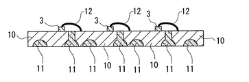
- an optical semiconductor device shown in FIG. 2 and FIG. can give. That is, in this optical semiconductor device, the optical semiconductor elements 3 are respectively mounted at predetermined positions on one surface in the thickness direction of the metal lead frames 10 arranged at intervals, and the gap between the metal lead frames 10 is in accordance with the present invention.
- the light reflection reflector 11 made of an epoxy resin composition is formed.
- the reflector 11 formed by filling the epoxy resin composition of the present invention in the gap between the metal lead frames 10 and curing is formed.
- reference numeral 12 denotes a bonding wire for electrically connecting the optical semiconductor element 3 and the metal lead frame 10.
- the metal lead frame 10 is placed in a mold of a transfer molding machine, and the gap between the metal lead frames 10 arranged at intervals and the optical semiconductor of the metal lead frame 10 are formed by transfer molding.
- the reflectors 11 are respectively formed by filling the epoxy resin composition in the recesses formed on the surface opposite to the element 3 mounting surface, and curing it.
- the optical semiconductor element 3 is mounted in the optical semiconductor element mounting region at a predetermined position of the metal lead frame 10
- the optical semiconductor element 3 and the metal lead frame 10 are electrically connected using the bonding wire 12. In this manner, the optical semiconductor device shown in FIGS. 2 and 3 is manufactured.
- FIG. 4 shows a sealed optical semiconductor element using the epoxy resin composition of the present invention as a reflector forming material. That is, in this sealed optical semiconductor element, a light reflecting reflector 15 made of the epoxy resin composition of the present invention is formed on the entire side surface of the optical semiconductor element 3, and an upper portion (light emitting surface or The light receiving surface is covered with the sealing layer 16.
- 17 is a connection electrode (bump).
- the sealing layer 16 is formed of an epoxy resin, a silicone resin, or an inorganic material such as glass or ceramics.
- the sealing layer 16 may contain a phosphor or is not blended with a phosphor. It may be a thing.
- Such a sealed optical semiconductor element can be manufactured, for example, as follows. That is, a flip chip type optical semiconductor (light emitting) element 3 (for example, a blue LED chip) is provided on an adhesive surface such as a dicing tape, and connection electrodes (bumps) 17 provided on the surface opposite to the light emitting surface are provided. Arranged at a fixed interval in a state of being embedded in the tape surface. Subsequently, all the side surfaces of the optical semiconductor element 3 and further the light emitting surface are embedded with the epoxy resin composition of the present invention using a compression molding machine, a transfer molding machine, or an injection molding machine.
- a flip chip type optical semiconductor (light emitting) element 3 for example, a blue LED chip
- connection electrodes (bumps) 17 provided on the surface opposite to the light emitting surface
- the thermosetting reaction of the said epoxy resin composition is completed, and the reflector 15 for light reflection which consists of the epoxy resin composition of this invention is formed in all the side surfaces of the optical semiconductor element 3.
- the light emitting surface is exposed by grinding and removing the reflector 15 formed on the light emitting surface, and a sealing material such as a silicone resin is surrounded by a dam material on the exposed light emitting surface.
- the sealing layer 16 is formed by casting in a state or by sticking a sheet-like sealing material to the light emitting surface.
- the center line between the optical semiconductor elements 3 is diced by using a blade dicer to separate each element. Then, the dicing tape is extended and stretched to reduce stickiness, and the sealed optical semiconductor elements 3 on which the reflectors 15 on the dicing tape are formed are completely separated and separated into individual pieces, as shown in FIG.
- the sealed optical semiconductor element 3 can be manufactured.
- connection electrode 17 of the optical semiconductor element 3 is provided at a predetermined position where a circuit of a printed circuit board is formed.
- each component shown below was prepared prior to the preparation of the epoxy resin composition.
- measuring agent b2 1,2,3,6-tetrahydrophthalic anhydride (solid) (manufactured by Shin Nippon Chemical Co., Ltd., Ricacid TH-PA)
- Examples 1 to 8 Comparative Examples 1 to 5
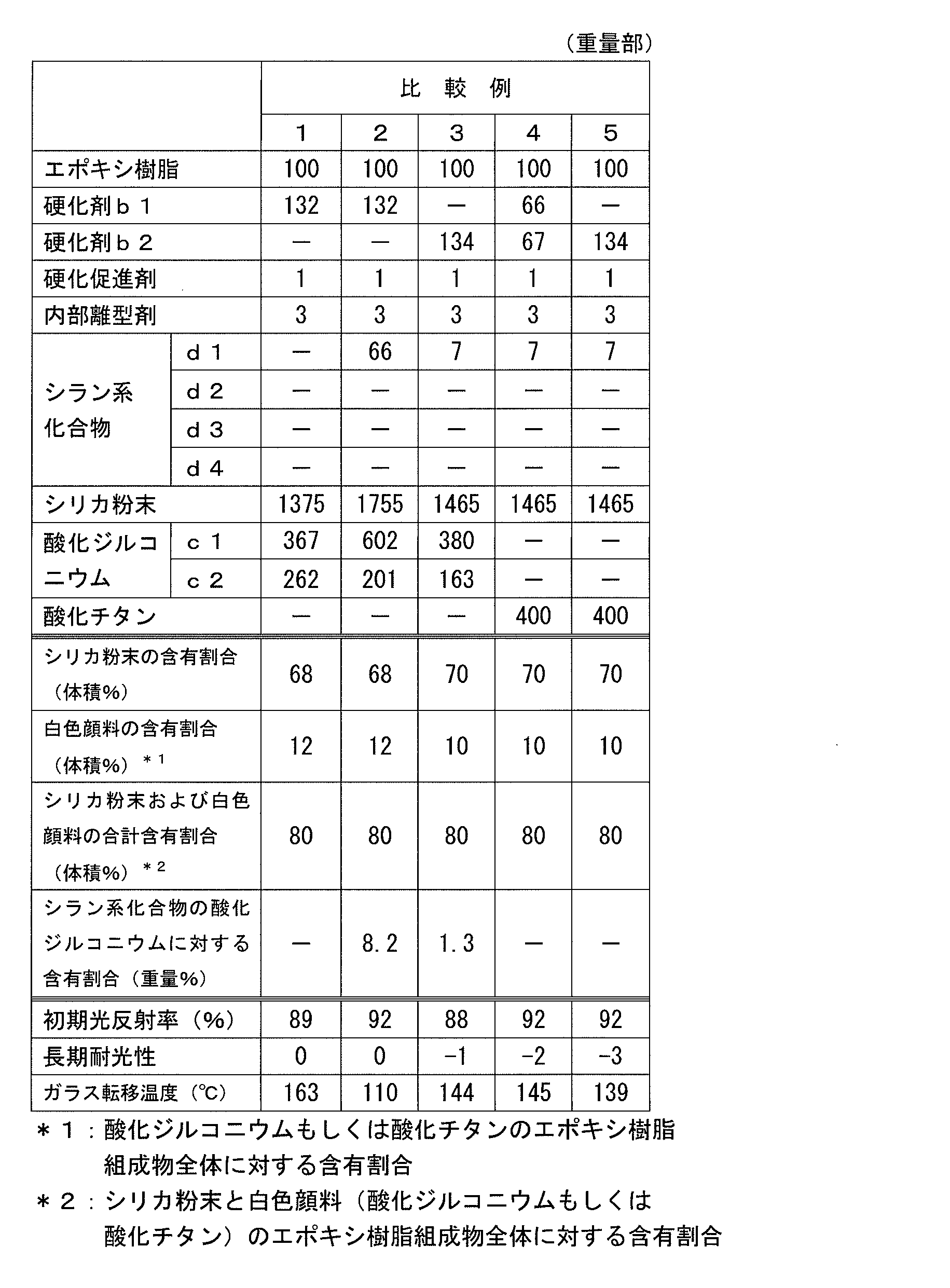
- the components shown in Tables 1 and 2 below are blended in the proportions shown in the same table, melt kneaded (temperature 100 to 130 ° C.) with a kneader, aged, cooled to room temperature (25 ° C.) and pulverized. Thus, a desired powdery epoxy resin composition was prepared.
- Example products comprising a liquid curing agent as a main component and containing zirconium oxide and a specific amount of a silane compound have excellent results not only for high initial light reflectance but also for long-term light resistance. Obtained. Moreover, it has a high glass transition temperature.
- Comparative Example 1 the product of Comparative Example 1 in which no silane compound was used resulted in inferior initial light reflectance.
- Comparative Example 2 using excessive amount of the silane-based compound gave the evaluation results of about the same level as the Examples with respect to the initial light reflectance and long-term light resistance, but the glass transition temperature was extremely low. there were.
- curing agent resulted in inferior to initial stage light reflectivity and long-term light resistance.
- Comparative Examples 4 and 5 using titanium oxide as a white pigment obtained evaluation results of substantially the same degree as the Examples with respect to the initial light reflectance, but both were inferior in long-term light resistance, and in particular solid In Comparative Example 5 using a curing agent, the glass transition temperature was lower.
- an optical semiconductor (light-emitting) device having the configuration shown in FIG. 1 was manufactured using a tablet-like epoxy resin composition obtained by tableting the powders of the above-mentioned examples. That is, a metal lead frame composed of a first plate portion 1 and a second plate portion 2 made of copper (silver plating) is placed in a mold of a transfer molding machine, and transfer molding is performed using the epoxy resin composition. By performing (condition: molding at 175 ° C. ⁇ 2 minutes + curing at 175 ° C. ⁇ 3 hours), the reflector 4 was formed at a predetermined position of the metal lead frame shown in FIG.
- an optical semiconductor (light emitting) element (size: 0.5 mm ⁇ 0.5 mm) 3 is mounted, and the optical semiconductor element 3 and the metal lead frame are electrically connected by bonding wires 7 and 8.
- a unit including the reflector 4, the metal lead frame, and the optical semiconductor element 3 was manufactured.
- a recess 5 formed by the metal lead frame and the inner peripheral surface of the reflector 4 is filled with a silicone resin (manufactured by Shin-Etsu Silicone Co., Ltd., KER-2500), and the optical semiconductor element 3 is resin-sealed (molded).
- a transparent sealing resin layer 6 was formed, and each reflector was separated into pieces by dicing to produce the optical semiconductor (light emitting) device shown in FIG.
- the obtained optical semiconductor (light emitting) device was provided with the reflector 4 excellent in long-term light resistance with a high initial light reflectance, and a good one with high reliability was obtained.
- the optical semiconductor device shown in FIGS. 2 and 3 and the sealed optical semiconductor element shown in FIG. 4 were produced according to the above-described manufacturing method.
- the obtained optical semiconductor device a good one having high reliability was obtained as described above.
- an optical semiconductor device is fabricated by mounting the obtained sealed optical semiconductor element through a connection electrode of the sealed optical semiconductor element at a predetermined position where the circuit of the printed circuit board is formed. did.
- a good one having high reliability was obtained as described above.
- the epoxy resin composition for optical semiconductor devices of the present invention is useful as a reflector forming material that reflects light emitted from an optical semiconductor element incorporated in the optical semiconductor device.
Landscapes
- Chemical & Material Sciences (AREA)
- Health & Medical Sciences (AREA)
- Chemical Kinetics & Catalysis (AREA)
- Medicinal Chemistry (AREA)
- Polymers & Plastics (AREA)
- Organic Chemistry (AREA)
- Led Device Packages (AREA)
- Compositions Of Macromolecular Compounds (AREA)
- Structures Or Materials For Encapsulating Or Coating Semiconductor Devices Or Solid State Devices (AREA)
- Epoxy Resins (AREA)
Abstract
Description
(A)エポキシ樹脂。
(B)液状硬化剤を主成分とする硬化剤。
(C)酸化ジルコニウム。
(D)シラン系化合物。
(E)無機質充填剤。
以下、本発明について詳細に説明する。
上記エポキシ樹脂(A成分)としては、ビスフェノールA型エポキシ樹脂、ビスフェノールF型エポキシ樹脂、ビスフェノールS型エポキシ樹脂、フェノールノボラック型エポキシ樹脂やクレゾールノボラック型エポキシ樹脂等のノボラック型エポキシ樹脂、モノグリシジルイソシアヌレート、ジグリシジルイソシアヌレート、トリグリシジルイソシアヌレート、ヒダントインエポキシ樹脂等の含窒素環エポキシ樹脂、水素添加ビスフェノールA型エポキシ樹脂、水素添加ビスフェノールF型エポキシ樹脂、脂肪族系エポキシ樹脂、シリコーン変性エポキシ樹脂、グリシジルエーテル型エポキシ樹脂、アルキル置換ビスフェノール等のジグリシジルエーテル、ジアミノジフェニルメタンおよびイソシアヌル酸等のポリアミンとエピクロルヒドリンとの反応により得られるグリシジルアミン型エポキシ樹脂、オレフィン結合を過酢酸等の過酸で酸化して得られる線状脂肪族および脂環式エポキシ樹脂、低吸水率硬化体タイプの主流であるビフェニル型エポキシ樹脂、ジシクロ環型エポキシ樹脂、ナフタレン型エポキシ樹脂等があげられる。これらは単独でもしくは2種以上併せて用いることができる。これらエポキシ樹脂の中でも、透明性および耐変色性に優れるという点から、脂環式エポキシ樹脂や、トリグリシジルイソシアヌレート等のイソシアヌル環構造を有するものを単独でもしくは併せて用いることが好ましい。同様の理由から、フタル酸、テトラヒドロフタル酸、ヘキサヒドロフタル酸、メチルテトラヒドロフタル酸、ナジック酸、メチルナジック酸等のジカルボン酸のジグリシジルエステルも好適である。また、芳香環が水素化された脂環式構造を有する核水素化トリメリット酸、核水素化ピロメリット酸等のグリシジルエステル等もあげられる。
本発明において、硬化剤(B成分)とは、液状硬化剤を主成分とするものであり、先に述べたように、硬化剤成分が液状硬化剤のみからなる場合を含む。具体的には、液状硬化剤が硬化剤全体の40重量%以上を占めることが好ましく、特に好ましくは硬化剤成分が液状硬化剤のみで構成されることである。なお、上記液状硬化剤とは、室温(25℃)下において液状を呈する硬化剤のことである。そして、このような液状硬化剤としては、例えば、耐熱性および耐光性の観点から、液状を呈する酸無水物系硬化剤等があげられる。
上記A成分およびB成分とともに用いられる酸化ジルコニウム(C成分)は、本発明において白色顔料として用いられるものである。上記酸化ジルコニウムには、単斜晶,正方晶,立方晶等の複数の結晶系があるが、中でも単斜晶の酸化ジルコニウムを用いることがコスト等の点から好ましい。上記酸化ジルコニウムとして、流動性等の観点から、平均粒径が0.01~50μmのものを用いることが好ましく、より好ましくは0.1~30μmであり、特に好ましくは0.1~20μmである。なお、上記平均粒径は、例えば、レーザー回折散乱式粒度分布計を用いて測定することができる。
上記シラン系化合物(D成分)としては、各種シラン系化合物、例えば、下記の一般式(1)で表されるシラン系化合物があげられる。
[式(1)において、XはCH3O-またはC2H5O-、RはCH3-またはC2H5-、R′は-CmH2m+1,-CH=CH2,-C6H5または-R″Y〔mは1~12の正数、R″は-CH2-,-CH2CH2-または-CH2CH2CH2-、Yはグリシジルエーテル基、3,4-エポキシシクロヘキシル基、-OOC(CH3)C=CH2、-NH2または-NHCH2CH2NH2である。〕、nは1,2または3である。]
上記A~D成分にとともに用いられる無機質充填剤(E成分)としては、例えば、石英ガラス粉末、タルク、溶融シリカ粉末や結晶性シリカ粉末等のシリカ粉末、アルミナ粉末、窒化アルミニウム粉末、窒化ケイ素粉末等があげられる。中でも、線膨張係数の低減等の観点から、溶融シリカ粉末を用いることが好ましく、特に高充填性および高流動性という観点から、溶融球状シリカ粉末を用いることが好ましい。なお、無機質充填剤(E成分)は、上記酸化ジルコニウム(C成分)を除く。上記無機質充填剤(E成分)の粒径およびその分布に関しては、上記酸化ジルコニウム(C成分)の粒径およびその分布との組み合わせを、エポキシ樹脂組成物をトランスファー成形等により成形する際のバリ等が最も低減するように配慮することが好ましい。具体的には、無機質充填剤(E成分)の平均粒径は、5~100μmであることが好ましく、特に好ましくは10~80μmである。なお、上記平均粒径は、前述と同様、例えば、レーザー回折散乱式粒度分布計を用いて測定することができる。
そして、本発明のエポキシ樹脂組成物には、上記A~E成分以外に、必要に応じて、硬化促進剤、離型剤を配合することができる。さらには、変性剤(可塑剤)、酸化防止剤、難燃剤、消泡剤、レベリング剤、紫外線吸収剤等の各種添加剤を適宜配合することができる。
[式(2)中、Rm,Rnは水素原子または一価のアルキル基であり、両者は互いに同じであっても異なっていてもよい。また、kは1~100の正数であり、xは1~100の正数である。]
本発明のエポキシ樹脂組成物は、例えば、つぎのようにして製造することができる。すなわち、上記A~E成分、さらには硬化促進剤および離型剤、ならびに必要に応じて用いられる各種添加剤を適宜配合した後、混練機等を用いて溶融混合し、ついで、これを冷却し固化して粉砕することにより粉末状のエポキシ樹脂組成物を製造することができる。
本発明のエポキシ樹脂組成物を用いてなる光半導体装置は、例えば、つぎのようにして製造される。すなわち、金属リードフレームをトランスファー成形機の金型内に設置して上記エポキシ樹脂組成物を用いてトランスファー成形によりリフレクタを形成する。このようにして、光半導体素子搭載領域の周囲を囲うように環状のリフレクタが形成されてなる光半導体装置用の金属リードフレームを作製する。ついで、上記リフレクタの内部の、金属リードフレーム上の光半導体素子搭載領域に光半導体素子を搭載し、光半導体素子と金属リードフレームとをボンディングワイヤーを用いて電気的に接続する。そして、上記光半導体素子を含むリフレクタの内側領域を、シリコーン樹脂等を用いて樹脂封止することにより封止樹脂層が形成される。このようにして、例えば、図1に示す立体状(カップ型)の光半導体装置が作製される。この光半導体装置は、前述のとおり、第1のプレート部1と第2のプレート部2とからなる金属リードフレームの第2のプレート部2上に光半導体素子3が搭載され、上記光半導体素子3の周囲を囲むように、本発明のエポキシ樹脂組成物からなる光反射用のリフレクタ4が形成されているという構成をとる。そして、上記金属リードフレームとリフレクタ4の内周面とで形成される凹部5には、光半導体素子3を封止する透明性を有する封止樹脂層6が形成されている。この封止樹脂層6には必要に応じて蛍光体が含有されている。図1において、7,8は金属リードフレームと光半導体素子3とを電気的に接続するボンディングワイヤーである。
さらに、本発明のエポキシ樹脂組成物をリフレクタ形成材料として用いた封止型光半導体素子を、図4に示す。すなわち、この封止型光半導体素子は、光半導体素子3の側面全部に本発明のエポキシ樹脂組成物からなる光反射用のリフレクタ15が形成され、さらに上記光半導体素子3の上部(発光面あるいは受光面)が封止層16にて被覆されているという構成をとる。図において、17は接続用電極(バンプ)である。また、上記封止層16はエポキシ樹脂やシリコーン樹脂、あるいはガラスやセラミックス等の無機材料によって形成され、上記封止層16には蛍光体が含有されていてもよいし蛍光体が配合されていないものであってもよい。
トリグリシジルイソシアヌレート(エポキシ当量100)
4-メチルヘキサヒドロ無水フタル酸(x)とヘキサヒドロ無水フタル酸(y)の混合物(液体、混合重量比x/y=70/30)(新日本理化社製、リカシッドMH-700)
[硬化剤b2]
1,2,3,6-テトラヒドロ無水フタル酸(固体)(新日本理化社製、リカシッドTH-PA)
第一稀元素化学工業社製、SG酸化ジルコニウム、単斜晶、屈折率2.1、平均粒径4.3μm
[酸化ジルコニウムc2]
第一稀元素化学工業社製、UEP酸化ジルコニウム、単斜晶、屈折率2.1、平均粒径0.5μm
堺化学工業社製、FTR-700、ルチル型、単一粒子径0.2μm
3-グリシドキシプロピルトリメトキシシラン(信越化学工業社製、KBM-403)
[シラン系化合物d2]
3-メタクリロキシプロピルトリメトキシシラン(信越化学工業社製、KBM-503)
[シラン系化合物d3]
フェニルトリメトキシシラン(信越化学工業社製、KBM-103)
[シラン系化合物d4]
ビニルトリメトキシシラン(東レ・ダウコーニング社製、SZ6300)
溶融球状シリカ粉末(平均粒径20μm)
メチルトリブチルホスホニウムジメチルホスフェート(日本化学工業社製、ヒシコーリンPX-4MP)
C(炭素数)>14、エトキシ化アルコール/エチレンホモポリマー(丸菱油化工業社製、UNT-750)
後記の表1~表2に示す各成分を同表に示す割合で配合し、ニーダーで溶融混練(温度100~130℃)を行ない、熟成した後、室温(25℃)まで冷却して粉砕することにより目的とする粉末状のエポキシ樹脂組成物を作製した。
上記各エポキシ樹脂組成物を用い、厚み1mmの試験片を所定の硬化条件(条件:175℃×2分間の成形+175℃×3時間キュア)にて作製し、この試験片(硬化物)を用いて、室温(25℃)での光反射率を測定した。なお、測定装置として日本分光社製の分光光度計V-670を使用して、波長450nmの光反射率を室温(25℃)にて測定した。
上記と同様にして作製した各試験片を用い、波長600nmの光反射率を室温(25℃)にて測定した。その後、その試験片を110℃のホットプレートで加熱した状態で、強度1W/cm2の高圧水銀灯の光を、g線(436nm)バンドパスフィルターを通して15分間照射した後に、上記と同様にして波長600nmの光反射率を測定した(加速試験)。そして、上記加速試験前後での光反射率の低下度(光照射後の光反射率-光照射前の光反射率)を算出した。なお、測定には、上記と同様、日本分光社製の分光光度計V-670を使用した。
上記各エポキシ樹脂組成物を用い、所定の硬化条件(条件:175℃×2分間の成形+175℃×3時間キュア)にて長さ20mmの角柱状の試験片を作製し、熱機械分析装置[島津製作所社製、TMA-50]にて測定した。

つぎに、上記実施例品である粉末を打錠したタブレット状のエポキシ樹脂組成物を用いて、図1に示す構成の光半導体(発光)装置を製造した。すなわち、銅(銀メッキ)製の第1のプレート部1と第2のプレート部2とからなる金属リードフレームをトランスファー成形機の金型内に設置し、上記エポキシ樹脂組成物を用いてトランスファー成形(条件:175℃×2分間の成形+175℃×3時間キュア)を行なうことにより、図1に示す、金属リードフレームの所定位置にリフレクタ4を形成した。ついで、光半導体(発光)素子(大きさ:0.5mm×0.5mm)3を搭載し、この光半導体素子3と上記金属リードフレームをボンディングワイヤー7,8にて電気的に接続することにより、リフレクタ4と、金属リードフレームと、光半導体素子3とを備えたユニットを製造した。
2 第2のプレート部
3 光半導体素子
4,11,15 リフレクタ
5 凹部
6 封止樹脂層
7,8,12 ボンディングワイヤー
10 金属リードフレーム
16 封止層
Claims (13)
- 下記の(A)~(E)を含有し、下記(C)および(E)の合計含有量が、エポキシ樹脂組成物全体の70~90体積%であり、かつ下記(D)の含有量が、下記(C)に対して0.1~8重量%であることを特徴とする光半導体装置用エポキシ樹脂組成物。
(A)エポキシ樹脂。
(B)液状硬化剤を主成分とする硬化剤。
(C)酸化ジルコニウム。
(D)シラン系化合物。
(E)無機質充填剤。 - 上記(D)が、下記の一般式(1)で表されるシラン系化合物から選ばれた少なくとも一つである請求項1記載の光半導体装置用エポキシ樹脂組成物。
(X)n(R)3-nSi(R′) ・・・(1)
[式(1)において、XはCH3O-またはC2H5O-、RはCH3-またはC2H5-、R′は-CmH2m+1,-CH=CH2,-C6H5または-R″Y〔mは1~12の正数、R″は-CH2-,-CH2CH2-または-CH2CH2CH2-、Yはグリシジルエーテル基、3,4-エポキシシクロヘキシル基、-OOC(CH3)C=CH2、-NH2または-NHCH2CH2NH2である。〕、nは1,2または3である。] - 上記(B)における液状硬化剤の占める割合が(B)全体の40重量%以上である請求項1または2記載の光半導体装置用エポキシ樹脂組成物。
- 上記(D)が、3-グリシドキシプロピルトリメトキシシラン、3-メタクリロキシプロピルトリメトキシシラン、フェニルトリメトキシシランおよびビニルトリメトキシシランからなる群から選ばれた少なくとも一つである請求項1~3のいずれか一項に記載の光半導体装置用エポキシ樹脂組成物。
- 厚み方向の片面のみに光半導体素子を搭載するための板状の光半導体装置用リードフレームであって、互いに隙間を隔てて配置される複数のプレート部を備えるとともに、上記隙間に、請求項1~4のいずれか一項に記載の光半導体装置用エポキシ樹脂組成物を用いて充填し、硬化してなるリフレクタが形成されてなることを特徴とする光半導体装置用リードフレーム。
- 光半導体素子搭載領域を備え、それ自体の少なくとも一部で素子搭載領域の周囲を囲んだ状態でリフレクタが形成されてなる立体状の光半導体装置用リードフレームであって、上記リフレクタが、請求項1~4のいずれか一項に記載の光半導体装置用エポキシ樹脂組成物を用いて形成されてなることを特徴とする光半導体装置用リードフレーム。
- 上記リフレクタが、リードフレームの片面にのみ形成されている請求項5または6記載の光半導体装置用リードフレーム。
- 上記リフレクタがトランスファー成形または射出成形により光半導体装置用リードフレームに形成されてなる請求項5~7のいずれか一項に記載の光半導体装置用リードフレーム。
- その片面に光半導体素子を搭載するための素子搭載領域を有するプレート部が、互いに隙間を隔てて配置され、上記素子搭載領域の所定位置に光半導体素子が搭載されてなる光半導体装置であって、上記隙間に、請求項1~4のいずれか一項に記載の光半導体装置用エポキシ樹脂組成物を用いて充填し、硬化してなるリフレクタが形成されてなることを特徴とする光半導体装置。
- 光半導体素子搭載領域を備え、それ自体の少なくとも一部で素子搭載領域の周囲を囲んだ状態でリフレクタが形成されてなる光半導体装置用リードフレームの所定位置に光半導体素子が搭載されてなる光半導体装置であって、上記リフレクタが、請求項1~4のいずれか一項に記載の光半導体装置用エポキシ樹脂組成物を用いて形成されてなることを特徴とする光半導体装置。
- リフレクタで囲まれた光半導体素子を含む領域をシリコーン樹脂にて樹脂封止されてなる請求項10記載の光半導体装置。
- 裏面に複数の接続用電極が形成されてなる光半導体素子の側面に請求項1~4のいずれか一項に記載の光半導体装置用エポキシ樹脂組成物からなるリフレクタが形成され、上記光半導体素子上部の発光面あるいは受光面が封止層にて被覆されてなることを特徴とする封止型光半導体素子。
- 配線回路基板の所定位置に、請求項12記載の封止型光半導体素子が、その接続用電極を介して搭載されてなる光半導体装置。
Priority Applications (2)
| Application Number | Priority Date | Filing Date | Title |
|---|---|---|---|
| CN201480046965.2A CN105493302A (zh) | 2013-12-04 | 2014-11-18 | 光半导体装置用环氧树脂组合物及使用其得到的光半导体装置用引线框、封装型光半导体元件以及光半导体装置 |
| KR1020167004800A KR20160094365A (ko) | 2013-12-04 | 2014-11-18 | 광반도체 장치용 에폭시 수지 조성물 및 그것을 이용하여 얻어지는 광반도체 장치용 리드 프레임, 밀봉형 광반도체 소자 및 광반도체 장치 |
Applications Claiming Priority (4)
| Application Number | Priority Date | Filing Date | Title |
|---|---|---|---|
| JP2013251257 | 2013-12-04 | ||
| JP2013-251257 | 2013-12-04 | ||
| JP2014-085151 | 2014-04-17 | ||
| JP2014085151A JP2015130476A (ja) | 2013-12-04 | 2014-04-17 | 光半導体装置用エポキシ樹脂組成物およびそれを用いて得られる光半導体装置用リードフレーム、封止型光半導体素子ならびに光半導体装置 |
Publications (1)
| Publication Number | Publication Date |
|---|---|
| WO2015083532A1 true WO2015083532A1 (ja) | 2015-06-11 |
Family
ID=53273299
Family Applications (1)
| Application Number | Title | Priority Date | Filing Date |
|---|---|---|---|
| PCT/JP2014/080410 Ceased WO2015083532A1 (ja) | 2013-12-04 | 2014-11-18 | 光半導体装置用エポキシ樹脂組成物およびそれを用いて得られる光半導体装置用リードフレーム、封止型光半導体素子ならびに光半導体装置 |
Country Status (5)
| Country | Link |
|---|---|
| JP (1) | JP2015130476A (ja) |
| KR (1) | KR20160094365A (ja) |
| CN (1) | CN105493302A (ja) |
| TW (1) | TW201527408A (ja) |
| WO (1) | WO2015083532A1 (ja) |
Families Citing this family (4)
| Publication number | Priority date | Publication date | Assignee | Title |
|---|---|---|---|---|
| JP6772841B2 (ja) * | 2015-02-05 | 2020-10-21 | 味の素株式会社 | 樹脂組成物 |
| JP7031287B2 (ja) * | 2016-12-22 | 2022-03-08 | Mcppイノベーション合同会社 | 3次元網目状構造体 |
| JP6926018B2 (ja) * | 2018-03-28 | 2021-08-25 | 東レエンジニアリング株式会社 | 転写基板ならびにこれを用いた実装方法および画像表示装置の製造方法 |
| JP7567317B2 (ja) * | 2020-09-24 | 2024-10-16 | 株式会社レゾナック | 光反射用熱硬化性樹脂組成物、光半導体素子搭載用基板及び光半導体装置 |
Citations (3)
| Publication number | Priority date | Publication date | Assignee | Title |
|---|---|---|---|---|
| JP2007234637A (ja) * | 2006-02-27 | 2007-09-13 | Kyocera Corp | 発光装置およびそれを用いた照明装置 |
| JP2010189553A (ja) * | 2009-02-18 | 2010-09-02 | Hitachi Chem Co Ltd | 光反射用熱硬化性樹脂組成物、光半導体素子搭載用基板及びその製造方法、並びに光半導体装置 |
| JP2013032442A (ja) * | 2011-08-02 | 2013-02-14 | Nitto Denko Corp | 光半導体装置用エポキシ樹脂組成物およびそれを用いて得られる光半導体装置用リードフレームまたは光半導体装置用基板、ならびに光半導体装置 |
Family Cites Families (6)
| Publication number | Priority date | Publication date | Assignee | Title |
|---|---|---|---|---|
| KR100911168B1 (ko) * | 2007-12-31 | 2009-08-06 | 제일모직주식회사 | 반도체 소자 밀봉용 에폭시 수지 조성물 및 이를 이용한 반도체 소자 |
| JP5721969B2 (ja) | 2010-06-11 | 2015-05-20 | 日東電工株式会社 | 光半導体装置のリフレクタ用エポキシ樹脂組成物およびそれを用いて得られる光半導体装置用リードフレーム、ならびに光半導体装置 |
| JP5745319B2 (ja) * | 2011-04-14 | 2015-07-08 | 日東電工株式会社 | 蛍光反射シート、および、発光ダイオード装置の製造方法 |
| JP2013110199A (ja) * | 2011-11-18 | 2013-06-06 | Citizen Electronics Co Ltd | Led発光装置 |
| JP5865038B2 (ja) * | 2011-11-30 | 2016-02-17 | 日東電工株式会社 | 素子接続用基板、その製造方法および発光ダイオード装置 |
| JP5970835B2 (ja) * | 2012-02-02 | 2016-08-17 | 大日本印刷株式会社 | リードフレーム部材、樹脂付リードフレーム部材および半導体装置 |
-
2014
- 2014-04-17 JP JP2014085151A patent/JP2015130476A/ja active Pending
- 2014-11-18 WO PCT/JP2014/080410 patent/WO2015083532A1/ja not_active Ceased
- 2014-11-18 TW TW103139903A patent/TW201527408A/zh unknown
- 2014-11-18 CN CN201480046965.2A patent/CN105493302A/zh active Pending
- 2014-11-18 KR KR1020167004800A patent/KR20160094365A/ko not_active Withdrawn
Patent Citations (3)
| Publication number | Priority date | Publication date | Assignee | Title |
|---|---|---|---|---|
| JP2007234637A (ja) * | 2006-02-27 | 2007-09-13 | Kyocera Corp | 発光装置およびそれを用いた照明装置 |
| JP2010189553A (ja) * | 2009-02-18 | 2010-09-02 | Hitachi Chem Co Ltd | 光反射用熱硬化性樹脂組成物、光半導体素子搭載用基板及びその製造方法、並びに光半導体装置 |
| JP2013032442A (ja) * | 2011-08-02 | 2013-02-14 | Nitto Denko Corp | 光半導体装置用エポキシ樹脂組成物およびそれを用いて得られる光半導体装置用リードフレームまたは光半導体装置用基板、ならびに光半導体装置 |
Also Published As
| Publication number | Publication date |
|---|---|
| TW201527408A (zh) | 2015-07-16 |
| KR20160094365A (ko) | 2016-08-09 |
| JP2015130476A (ja) | 2015-07-16 |
| CN105493302A (zh) | 2016-04-13 |
Similar Documents
| Publication | Publication Date | Title |
|---|---|---|
| KR101787771B1 (ko) | 광반도체 장치용 에폭시 수지 조성물 및 그것을 사용해서 얻어지는 광반도체 장치용 리드 프레임 및 광반도체 장치용 기판, 및 광반도체 장치 | |
| JP5976806B2 (ja) | 光半導体装置用エポキシ樹脂組成物およびそれを用いて得られる光半導体装置用リードフレーム、封止型光半導体素子ならびに光半導体装置 | |
| JP2011060819A (ja) | 光半導体素子収納用実装パッケージ用樹脂組成物およびそれを用いて得られる光半導体発光装置 | |
| JP2012175030A (ja) | 光半導体素子収納用実装パッケージ用樹脂組成物およびそれを用いて得られる光半導体発光装置 | |
| CN102952370B (zh) | 光学半导体装置用环氧树脂组合物及使用其的光学半导体装置 | |
| JP2012077235A (ja) | 光半導体装置用エポキシ樹脂組成物およびそれを用いて得られる光半導体装置用リードフレーム、ならびに光半導体装置 | |
| JP5721969B2 (ja) | 光半導体装置のリフレクタ用エポキシ樹脂組成物およびそれを用いて得られる光半導体装置用リードフレーム、ならびに光半導体装置 | |
| WO2015083532A1 (ja) | 光半導体装置用エポキシ樹脂組成物およびそれを用いて得られる光半導体装置用リードフレーム、封止型光半導体素子ならびに光半導体装置 | |
| WO2015083576A1 (ja) | 光半導体装置用熱硬化性樹脂組成物およびそれを用いて得られる光半導体装置用リードフレーム、ならびに光半導体装置 | |
| JP5825650B2 (ja) | 光半導体リフレクタ用エポキシ樹脂組成物、光半導体装置用熱硬化性樹脂組成物およびそれを用いて得られる光半導体装置用リードフレーム、封止型光半導体素子ならびに光半導体装置 | |
| KR20160094367A (ko) | 광반도체 장치용 열경화성 수지 조성물 및 그것을 이용하여 얻어지는 광반도체 장치용 리드 프레임, 및 광반도체 장치 | |
| JP6883185B2 (ja) | 光半導体装置用熱硬化性樹脂組成物およびそれを用いて得られる光半導体装置用リードフレーム、光半導体装置、光半導体素子 | |
| JP2015000885A (ja) | 光半導体装置用エポキシ樹脂組成物およびそれを用いて得られる光半導体装置用リードフレーム、ならびに光半導体装置 | |
| WO2017051838A1 (ja) | 光半導体装置用熱硬化性樹脂組成物およびそれを用いて得られる光半導体装置用リードフレーム、光半導体装置、光半導体素子 |
Legal Events
| Date | Code | Title | Description |
|---|---|---|---|
| WWE | Wipo information: entry into national phase |
Ref document number: 201480046965.2 Country of ref document: CN |
|
| 121 | Ep: the epo has been informed by wipo that ep was designated in this application |
Ref document number: 14867531 Country of ref document: EP Kind code of ref document: A1 |
|
| ENP | Entry into the national phase |
Ref document number: 20167004800 Country of ref document: KR Kind code of ref document: A |
|
| NENP | Non-entry into the national phase |
Ref country code: DE |
|
| 122 | Ep: pct application non-entry in european phase |
Ref document number: 14867531 Country of ref document: EP Kind code of ref document: A1 |